Introduction to EMI/EMC Challenges and Their Solution
|
|
|
- Justina Lambert
- 6 years ago
- Views:
Transcription


1 Introduction to EMI/EMC Challenges and Their Solution Dr. Hany Fahmy HSD Application Expert Agilent Technologies Davy Pissort, K.U. Leuven Charles Jackson, Nvidia Charlie Shu, Nvidia Chen Wang, Nvidia Amolak Badesha, Avago
 Not optimal Does not always work Costly Copper band-aid R4N Suppressor")
2 Current Solution Put on a bandaid to stop the Bleeding (radiation..) Not optimal Does not always work Costly Copper band-aid R4N Suppressor band-aid

3 Complexity of EMI problem I/Os can inject Common-mode Noise Or Power-pins inject Noise into PDN Badly routed traces generate EMI High-speed connectors and cables amplify the EMI problems Connectors M INIMIZE IC, PKG, AND PCB EMI TO R EDUCE O VERALL S YSTEM EMI High-speed PCB High-speed IC * From EM-Scan Measurement of GPU Board
4 Mechanism of Noise Propagation Noise Source (2) Radiation Noise (1) Conductive Noise Equipment or device exposed to noise Noise Source (3) Conductive Noise Equipment or device exposed to noise Noise Source Conductive Noise Equipment or device exposed to noise


5 Different types of Emission Trace-Emission I/O-Buffers Injecting Signal GND Return-currents & Slots Power-Pins Injecting Noise Common-Mode noise travelling through Connectors

6 Introducing the concept of Virtual-EMI Lab O PTIMIZE FOR EMI D EVELOP EMI G UIDELINES V ALIDATION WITH M EASUREMENTS *Full-wave EM Simulation, What-if Analysis, Root-cause debugging **Measurements to Isolate the problem and Correlate with Simulation
7 Radiated-emission on packages due to return-path-discontinuity
 nets major referencing")
8 DDR3 Package Modeling using MOM DC to 20GHz Data- (DQ-) nets major referencing to GND


9 Routing of DQ signals from Die-Bumps-Top to Layer-3 running as Symmetric-SL sandwiched between GND on Layers 2 & 4 DQ signals on Layer-3 as Symmetric-SL DQ Die-Bumps


10 Moving from Layer-3 to Layer-6 through Signal- PTH to pickup the Balls DQ signals on Layer-6 routed between GND on layers 5 DQ signals on Layer-3


11 Impact of GND-PTH stitching: Proximity & # Original-Package: With 15-GND-PTH Cost-Reduced-Package: with 3-GND-PTH

12 Comparison of Return-current on GND-L4 Original-Package: Cost-Reduced-Package: With 15-GND-PTH With 3-GND-PTH Larger NEXT by 10dB


13 Comparison of 1.33GBps Original-Package: Cost-Reduced-Package: With 15-GND-PTH With 3-GND-PTH DQ 40ps loss of margin DQ +95ps worst Setup-Margin +55ps worst Setup-Margin DQS DQS
14 PKG-Antenna-Parameters Comparison of 15-GND-PTH compared to 3-GND-PTH Antenna-Gain -19dB -11dB (+8dB) Radiated-Power 40-uWatts 220-uWatts (6x) Maximum Intensity: 5u-watts/Steradian 40- uwatts/steradian (8X) Angle of U-max: 160-degrees vs. 140-degrees


15 Trade-off Low-cost & Performance Reducing # of GND-Stitches Medium-2-low-risk for 1.33GB/s operation with +55ps worst-case Setup-margin but with +8dB Antenna-Gain Most probably we need to Turn-ON Spread spectrum. What is the cost of PLL vs. Reduction of GND-Stitch?
16 Trace Emission on PCBs due to costreduction Low-Layer count PCB CASE:1 Memory emission from MA/CMD lanes

17 4-layer PCB with Memory Emission Problem Problem: Investigate Emission problem at 1.25 times the memory clock frequency (1.623 GHz) Notes: Address/Command Nets are routed on bottom-layer Referencing power plane (due to lack of real-estate)
")

18 EMI Simulation Methodology Step-1: Simulate and Visualize Current-density plot* Method-of-Moments (Momentum) Simulations showing current-density plots and hot-spot regions on the PCB Emscan Measurements *Using Agilent Momentum Field Solver

19 EMI Simulation Methodology, Cont Step-2: Isolate Problem Observe hot-spot area closely, and identify root-cause Root-cause: There is small λ/8 power-plane patch that is radiating like patch-antenna Use the Momentum-uwave EM-engine with Antenna-Gain parameter to measure the merit of the PCB as non-intended antenna Develop EMI guidelines along with SI/PI Guidelines using Antenna-Gain Parameter to compare Layout guidelines

20 What is the remedy? Instead of REF MA/CMD to a VddQ Patch on Bottom layer continue routing on Bottom Layer 3m Chamber at least 16dB Improvement
21 Trace Emission on PCBs due to costreduction Low-Layer count PCB CASE:2 TMDS Emissions

22 Problem Statement TMDS 770MHz on 4-layer PCB & Coupling to Neighbor Ethernet-Card

23 Which one is better Copper band-aid R4N Suppressor band-aid

24

25


26 Is it E-coupling or H-coupling? With Metallic Shield *Lab data confirms simulation results Solution: Simulation shows that suppression material is improving EMI emission, whereas, metallic shied is making it worse Choose Suppression material over metallic shied -> Improve both cost and performance


27 Near-field scan results R4N Suppressor band-aid Emscan measurements

28

29

30 What is the Remedy? Sometimes it is cheaper to dampen the receiver not Emitter because adding R4N suppression materials is more cost than using RJ45 shielded connector on the Ethernet-card. Selected to change RJ45 Connector on Ethernet-card to shielded one to suppress the receiver
31 PCB Edge Emission due to Power delivery Noise

32 Simulation Challenges in EMI System level (source, coupling path, unintentional antenna Full wave simulation is often needed Time and memory consuming
33 Combining Measured Icc(t) with FDTD simulations to study the critical on-board-decaps under the GPU Power Delivery Network Current VddQ pins Drivers Channel Receivers SSO current is obtained by a combined simulation of the power delivery network model and the memory IO channel model

34 Measured Dynamic-current profile Icc(t) fft ifft steady-state frequencies Time-domain noise pattern directly imported into FDTD solver

35 Importing PCB layout of the Memory Channel Stackup 8 cm Signal Ground Signal VDD Ground VDD 11 cm board thickness: 1.57mm


36 SSO Noise Source on Top Layer Noise sources IC


37 Decaps on Bottom Layer decaps


38 Far-Field Radiation at 0.5 GHz at 1.0 GHz With Decaps Without Decaps With Decaps Without Decaps Reduction of 3-4 db
39 Current Density At 0.5 GHz At 0.5 GHz With Decaps Without Decaps
40 What is the benefit of PCB decaps? New method to optimize the PCB decaps: 1. Measure or simulate the Dynamic-current profile the VddQ-pins with maximum activity on the memory-channel 2. Import the Icc(t) into FDTD (wide-band-phenomena) 3. Study the critical PCB decaps to mitigate the SSO noise emission
41 Connector/Cable Emission


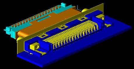

42 Board +Connector +Mate


43 Combining CAD and Board Files Precise landing of connector fingers on board signal pad
 Accelerated on GPU system Simulation time ½ day with 1-GPU card and 2-hrs with 3-GPU cards Study if improved grounding")
44 Near-Field Radiation: Do we need Shielded Connector? ($0.15 more cost) Do we need copper-tape under connector? Simulated with FDTD-solver (Agilent EMPro) Accelerated on GPU system Simulation time ½ day with 1-GPU card and 2-hrs with 3-GPU cards Study if improved grounding & shielding of the connector improves EMI behavior

45 Improved Grounding of the Connector: What is the impact of a copper-tape under the connector No copper tape Extra copper tape
46 Improved Grounding: Far-field impact of CU-tape Reduction of 5 db for EMI emission In direction of chassis
47 Conclusion Virtual-EMI Lab is a MUST for Speed-of-Light Product-to-Market Radiated/Conducted-Emission: Packages Return-Path-Discontinuity driving the need to turn-on SS ORDER A TRIAL VERSION PCBs due to Cost-Reduction 4L-PCBs MA/CMD Emission by referencing to VddQ FOR ADS TMDS Emission due to routing on Bottom layer SSO Noise Emission by VddQ Current-Profile on PCB Decaps are very effective Emission of Connector+Cables from HDMI common-mode noise sof-ads-si-evaluation
Why do we need to study Signal Integrity, Power Integrity and EMI ALL-AT-ONCE?
 Why do we need to study Signal Integrity, Power Integrity and EMI ALL-AT-ONCE? Hany Fahmy Riccardo Giacometti Cédric Pujol EMI HSD Signal Integrity Power Integrity An Example of Dramatic increase in HSD
How to anticipate Signal Integrity Issues: Improve my Channel Simulation by using Electromagnetic based model
 How to anticipate Signal Integrity Issues: Improve my Channel Simulation by using Electromagnetic based model HSD Strategic Intent Provide the industry s premier HSD EDA software. Integration of premier
PDS Impact for DDR Low Cost Design
 PDS Impact for DDR3-1600 Low Cost Design Jack W.C. Lin Sr. AE Manager jackl@cadence.com Aug. g 13 2013 Cadence, OrCAD, Allegro, Sigrity and the Cadence logo are trademarks of Cadence Design Systems, Inc.
Debugging EMI Using a Digital Oscilloscope. Dave Rishavy Product Manager - Oscilloscopes
 Debugging EMI Using a Digital Oscilloscope Dave Rishavy Product Manager - Oscilloscopes 06/2009 Nov 2010 Fundamentals Scope Seminar of DSOs Signal Fidelity 1 1 1 Debugging EMI Using a Digital Oscilloscope
Engineering the Power Delivery Network
 C HAPTER 1 Engineering the Power Delivery Network 1.1 What Is the Power Delivery Network (PDN) and Why Should I Care? The power delivery network consists of all the interconnects in the power supply path
Automotive PCB SI and PI analysis
 Automotive PCB SI and PI analysis SI PI Analysis Signal Integrity S-Parameter Timing analysis Eye diagram Power Integrity Loop / Partial inductance DC IR-Drop AC PDN Impedance Power Aware SI Signal Integrity
EMI. Chris Herrick. Applications Engineer
 Fundamentals of EMI Chris Herrick Ansoft Applications Engineer Three Basic Elements of EMC Conduction Coupling process EMI source Emission Space & Field Conductive Capacitive Inductive Radiative Low, Middle
Chapter 16 PCB Layout and Stackup
 Chapter 16 PCB Layout and Stackup Electromagnetic Compatibility Engineering by Henry W. Ott Foreword The PCB represents the physical implementation of the schematic. The proper design and layout of a printed
Heat Sink Design Flow for EMC
 DesignCon 2008 Heat Sink Design Flow for EMC Philippe Sochoux, Cisco Systems, Inc. psochoux@cisco.com Jinghan Yu, Cisco Systems, Inc. jinyu@cisco.com Alpesh U. Bhobe, Cisco Systems, Inc. abhobe@cisco.com
Chapter 12 Digital Circuit Radiation. Electromagnetic Compatibility Engineering. by Henry W. Ott
 Chapter 12 Digital Circuit Radiation Electromagnetic Compatibility Engineering by Henry W. Ott Forward Emission control should be treated as a design problem from the start, it should receive the necessary
High Speed Design Issues and Jitter Estimation Techniques. Jai Narayan Tripathi
 High Speed Design Issues and Jitter Estimation Techniques Jai Narayan Tripathi (jainarayan.tripathi@st.com) Outline Part 1 High-speed Design Issues Signal Integrity Power Integrity Jitter Power Delivery
Taking the Mystery out of Signal Integrity
 Slide - 1 Jan 2002 Taking the Mystery out of Signal Integrity Dr. Eric Bogatin, CTO, GigaTest Labs Signal Integrity Engineering and Training 134 S. Wolfe Rd Sunnyvale, CA 94086 408-524-2700 www.gigatest.com
A Co-design Methodology of Signal Integrity and Power Integrity
 DesignCon 2006 A Co-design Methodology of Signal Integrity and Power Integrity Woong Hwan Ryu, Intel Corporation woong.hwan.ryu@intel.com Min Wang, Intel Corporation min.wang@intel.com 1 Abstract As PCB
How EMxpert Diagnoses Board-Level EMC Design Issues
 Application Report EMxpert July 2011 - Cédric Caudron How EMxpert Diagnoses Board-Level EMC Design Issues ABSTRACT EMxpert provides board-level design teams with world-leading fast magnetic very-near-field
Relationship Between Signal Integrity and EMC
 Relationship Between Signal Integrity and EMC Presented by Hasnain Syed Solectron USA, Inc. RTP, North Carolina Email: HasnainSyed@solectron.com 06/05/2007 Hasnain Syed 1 What is Signal Integrity (SI)?
EMC cases study. Antonio Ciccomancini Scogna, CST of America CST COMPUTER SIMULATION TECHNOLOGY
 EMC cases study Antonio Ciccomancini Scogna, CST of America antonio.ciccomancini@cst.com Introduction Legal Compliance with EMC Standards without compliance products can not be released to the market Failure
Understanding the Unintended Antenna Behavior of a Product
 Understanding the Unintended Antenna Behavior of a Product Colin E. Brench Southwest Research Institute Electromagnetic Compatibility Research and Testing colin.brench@swri.org Radiating System Source
JANUARY 28-31, 2013 SANTA CLARA CONVENTION CENTER. World s First LPDDR3 Enabling for Mobile Application Processors System
 JANUARY 28-31, 2013 SANTA CLARA CONVENTION CENTER World s First LPDDR3 Enabling for Mobile Application Processors System Contents Introduction Problem Statements at Early mobile platform Root-cause, Enablers
Myoung Joon Choi, Vishram S. Pandit Intel Corp.
 Myoung Joon Choi, Vishram S. Pandit Intel Corp. IBIS Summit at DesignCon 2010 Acknowledgements: Woong Hwan Ryu, Joe Salmon Copyright 2010, Intel Corporation. All rights reserved. Need for SI/PI Co-analysis
Power integrity is more than decoupling capacitors The Power Integrity Ecosystem. Keysight HSD Seminar Mastering SI & PI Design
 Power integrity is more than decoupling capacitors The Power Integrity Ecosystem Keysight HSD Seminar Mastering SI & PI Design Signal Integrity Power Integrity SI and PI Eco-System Keysight Technologies
A NEW COMMON-MODE VOLTAGE PROBE FOR PREDICTING EMI FROM UNSHIELDED DIFFERENTIAL-PAIR CABLES
 A NEW COMMON-MODE VOLTAGE PROBE FOR PREDICTING EMI FROM UNSHIELDED DIFFERENTIAL-PAIR CABLES Neven Pischl Bay Networks Division of Nortel Networks Santa Clara, CA npischl@nortelnetworks.com (408) 495 3261
Top Ten EMC Problems & EMC Troubleshooting Techniques by Kenneth Wyatt, DVD, Colorado Springs Rev. 1, Feb 26, 2007
 EMC Engineering Top Ten EMC Problems & EMC Troubleshooting Techniques by Kenneth Wyatt, DVD, Colorado Springs Rev. 1, Feb 26, 2007 1a. Ground Impedance The overwhelming majority of high-frequency problems,
The Ground Myth IEEE. Bruce Archambeault, Ph.D. IBM Distinguished Engineer, IEEE Fellow 18 November 2008
 The Ground Myth Bruce Archambeault, Ph.D. IBM Distinguished Engineer, IEEE Fellow barch@us.ibm.com 18 November 2008 IEEE Introduction Electromagnetics can be scary Universities LOVE messy math EM is not
PCB. Electromagnetic radiation due to high speed logic from different PCB layouts. (First Draft)
") EMC CONSULTING INC. P.O. Box 496, Merrickville, Ontario, K0G 1N0 Phone: (613) 269-4247 Fax: (613) 269-2045 E-mail: emccons@magma.ca Web Page: www.emcconsultinginc.com PCB. Electromagnetic radiation due
EMC CONSULTING INC. P.O. Box 496, Merrickville, Ontario, K0G 1N0 Phone: (613) 269-4247 Fax: (613) 269-2045 E-mail: emccons@magma.ca Web Page: www.emcconsultinginc.com PCB. Electromagnetic radiation due
Predicting and Controlling Common Mode Noise from High Speed Differential Signals
 Predicting and Controlling Common Mode Noise from High Speed Differential Signals Bruce Archambeault, Ph.D. IEEE Fellow, inarte Certified Master EMC Design Engineer, Missouri University of Science & Technology
EMI Reduction on an Automotive Microcontroller
 EMI Reduction on an Automotive Microcontroller Design Automation Conference, July 26 th -31 st, 2009 Patrice JOUBERT DORIOL 1, Yamarita VILLAVICENCIO 2, Cristiano FORZAN 1, Mario ROTIGNI 1, Giovanni GRAZIOSI
Top Ten EMC Problems
 Top Ten EMC Problems presented by: Kenneth Wyatt Sr. EMC Consultant EMC & RF Design, Troubleshooting, Consulting & Training 10 Northern Boulevard, Suite 1 Amherst, New Hampshire 03031 +1 603 578 1842 www.silent-solutions.com
PCB Routing Guidelines for Signal Integrity and Power Integrity
 PCB Routing Guidelines for Signal Integrity and Power Integrity Presentation by Chris Heard Orange County chapter meeting November 18, 2015 1 Agenda Insertion Loss 101 PCB Design Guidelines For SI Simulation
Applications of 3D Electromagnetic Modeling in Magnetic Recording: ESD and Signal Integrity
 Applications of 3D Electromagnetic Modeling in Magnetic Recording: ESD and Signal Integrity CST NORTH AMERICAN USERS FORUM John Contreras 1 and Al Wallash 2 Hitachi Global Storage Technologies 1. San Jose
The number of layers The number and types of planes (power and/or ground) The ordering or sequence of the layers The spacing between the layers
 The ordering or sequence of the layers The spacing between the layers") PCB Layer Stackup PCB layer stackup (the ordering of the layers and the layer spacing) is an important factor in determining the EMC performance of a product. The following four factors are important with
PCB Layer Stackup PCB layer stackup (the ordering of the layers and the layer spacing) is an important factor in determining the EMC performance of a product. The following four factors are important with
Signal Integrity Modeling and Simulation for IC/Package Co-Design
 Signal Integrity Modeling and Simulation for IC/Package Co-Design Ching-Chao Huang Optimal Corp. October 24, 2004 Why IC and package co-design? The same IC in different packages may not work Package is
DL-150 The Ten Habits of Highly Successful Designers. or Design for Speed: A Designer s Survival Guide to Signal Integrity
 Slide -1 Ten Habits of Highly Successful Board Designers or Design for Speed: A Designer s Survival Guide to Signal Integrity with Dr. Eric Bogatin, Signal Integrity Evangelist, Bogatin Enterprises, www.bethesignal.com
Chip Package - PC Board Co-Design: Applying a Chip Power Model in System Power Integrity Analysis
 Chip Package - PC Board Co-Design: Applying a Chip Power Model in System Power Integrity Analysis Authors: Rick Brooks, Cisco, ricbrook@cisco.com Jane Lim, Cisco, honglim@cisco.com Udupi Harisharan, Cisco,
Effective Routing of Multiple Loads
 feature column BEYOND DESIGN Effective Routing of Multiple Loads by Barry Olney In a previous Beyond Design, Impedance Matching: Terminations, I discussed various termination strategies and concluded that
Optimization of Wafer Level Test Hardware using Signal Integrity Simulation
 June 7-10, 2009 San Diego, CA Optimization of Wafer Level Test Hardware using Signal Integrity Simulation Jason Mroczkowski Ryan Satrom Agenda Industry Drivers Wafer Scale Test Interface Simulation Simulation
Design Considerations for Highly Integrated 3D SiP for Mobile Applications
 Design Considerations for Highly Integrated 3D SiP for Mobile Applications FDIP, CA October 26, 2008 Joungho Kim at KAIST joungho@ee.kaist.ac.kr http://tera.kaist.ac.kr Contents I. Market and future direction
EMC problems from Common Mode Noise on High Speed Differential Signals
 EMC problems from Common Mode Noise on High Speed Differential Signals Bruce Archambeault, PhD Alma Jaze, Sam Connor, Jay Diepenbrock IBM barch@us.ibm.com 1 Differential Signals Commonly used for high
EMC Simulation of Consumer Electronic Devices
 of Consumer Electronic Devices By Andreas Barchanski Describing a workflow for the EMC simulation of a wireless router, using techniques that can be applied to a wide range of consumer electronic devices.
3D IC-Package-Board Co-analysis using 3D EM Simulation for Mobile Applications
 3D IC-Package-Board Co-analysis using 3D EM Simulation for Mobile Applications Darryl Kostka, CST of America Taigon Song and Sung Kyu Lim, Georgia Institute of Technology Outline Introduction TSV Array
PDN design and analysis methodology in SI&PI codesign
 PDN design and analysis methodology in SI&PI codesign www.huawei.com Asian IBIS Summit, November 9, 2010, Shenzhen China Luo Zipeng (luozipeng@huawei.com) Liu Shuyao (liushuyao@huawei.com) HUAWEI TECHNOLOGIES
Course Introduction Purpose Objectives Content Learning Time
 Course Introduction Purpose This course discusses techniques for analyzing and eliminating noise in microcontroller (MCU) and microprocessor (MPU) based embedded systems. Objectives Learn about a method
HOW SMALL PCB DESIGN TEAMS CAN SOLVE HIGH-SPEED DESIGN CHALLENGES WITH DESIGN RULE CHECKING MENTOR GRAPHICS
 HOW SMALL PCB DESIGN TEAMS CAN SOLVE HIGH-SPEED DESIGN CHALLENGES WITH DESIGN RULE CHECKING MENTOR GRAPHICS H I G H S P E E D D E S I G N W H I T E P A P E R w w w. p a d s. c o m INTRODUCTION Coping with
Technical Report Printed Circuit Board Decoupling Capacitor Performance For Optimum EMC Design
 Technical Report Printed Circuit Board Decoupling Capacitor Performance For Optimum EMC Design Bruce Archambeault, Ph.D. Doug White Personal Systems Group Electromagnetic Compatibility Center of Competency
through Electrical Performance Assessment Principal AE Aug
 An Alternative for Design Checking through Electrical Performance A Assessment t y Wu Paddy Principal AE Aug.13 2013 Agenda The Package/PCB Electrical Performance Checking Challenge Allegro Sigrity Integration
Low power SERDES transceiver for supply-induced jitter sensitivity methodology analysis
 Low power SERDES transceiver for supply-induced jitter sensitivity methodology analysis Micro Chang htc Michael_Chang@hTC.com Jan 9, 2019 X 1 Agenda Jitter-aware target impedance of power delivery network
Demystifying Vias in High-Speed PCB Design
 Demystifying Vias in High-Speed PCB Design Keysight HSD Seminar Mastering SI & PI Design db(s21) E H What is Via? Vertical Interconnect Access (VIA) An electrical connection between layers to pass a signal
The Challenges of Differential Bus Design
 The Challenges of Differential Bus Design February 20, 2002 presented by: Arthur Fraser TechKnowledge Page 1 Introduction Background Historically, differential interconnects were often twisted wire pairs
System Co-design and optimization for high performance and low power SoC s
 System Co-design and optimization for high performance and low power SoC s Siva S Kothamasu, Texas Instruments Inc, Dallas Snehamay Sinha, Texas Instruments Inc, Dallas Amit Brahme, Texas Instruments India
Cyclone III Simultaneous Switching Noise (SSN) Design Guidelines
 Design Guidelines") Cyclone III Simultaneous Switching Noise (SSN) Design Guidelines December 2007, ver. 1.0 Introduction Application Note 508 Low-cost FPGAs designed on 90-nm and 65-nm process technologies are made to support
Cyclone III Simultaneous Switching Noise (SSN) Design Guidelines December 2007, ver. 1.0 Introduction Application Note 508 Low-cost FPGAs designed on 90-nm and 65-nm process technologies are made to support
Effectively Using the EM 6992 Near Field Probe Kit to Troubleshoot EMI Issues
 Effectively Using the EM 6992 Near Field Probe Kit to Troubleshoot EMI Issues Introduction The EM 6992 Probe Kit includes three magnetic (H) field and two electric (E) field passive, near field probes
Minimizing Coupling of Power Supply Noise Between Digital and RF Circuit Blocks in Mixed Signal Systems
 Minimizing Coupling of Power Supply Noise Between Digital and RF Circuit Blocks in Mixed Signal Systems Satyanarayana Telikepalli, Madhavan Swaminathan, David Keezer Department of Electrical & Computer
Case Study Package Design & SI/PI analysis
 Caliber Interconnect Solutions Design for perfection Case Study Package Design & SI/PI analysis Caliber Interconnect Solutions (Pvt) Ltd No 6,1 st Street Gandhi Nagar, Kavundampalayam, Coimbatore-30. Tamil
How Long is Too Long? A Via Stub Electrical Performance Study
 How Long is Too Long? A Via Stub Electrical Performance Study Michael Rowlands, Endicott Interconnect Michael.rowlands@eitny.com, 607.755.5143 Jianzhuang Huang, Endicott Interconnect 1 Abstract As signal
The water-bed and the leaky bucket
 The water-bed and the leaky bucket Tim Williams Elmac Services Wareham, UK timw@elmac.co.uk Abstract The common situation of EMC mitigation measures having the opposite effect from what was intended, is
PI3HDMIxxx 4-Layer PCB Layout Guideline for HDMI Products
 PI3HDMIxxx 4-Layer PCB Layout Guideline for HDMI Products Introduction The differential trace impedance of HDMI is specified at 100Ω±15% in Test ID 8-8 in HDMI Compliance Test Specification Rev.1.2a and
ANSYS CPS SOLUTION FOR SIGNAL AND POWER INTEGRITY
 ANSYS CPS SOLUTION FOR SIGNAL AND POWER INTEGRITY Rémy FERNANDES Lead Application Engineer ANSYS 1 2018 ANSYS, Inc. February 2, 2018 ANSYS ANSYS - Engineering simulation software leader Our industry reach
Intel 82566/82562V Layout Checklist (version 1.0)
") Intel 82566/82562V Layout Checklist (version 1.0) Project Name Fab Revision Date Designer Intel Contact SECTION CHECK ITEMS REMARKS DONE General Ethernet Controller Obtain the most recent product documentation
Intel 82566/82562V Layout Checklist (version 1.0) Project Name Fab Revision Date Designer Intel Contact SECTION CHECK ITEMS REMARKS DONE General Ethernet Controller Obtain the most recent product documentation
DesignCon Control of Electromagnetic Radiation from Integrated Circuit Heat sinks. Cristian Tudor, Fidus Systems Inc.
 DesignCon 2009 Control of Electromagnetic Radiation from Integrated Circuit Heat sinks Cristian Tudor, Fidus Systems Inc. Cristian.Tudor@fidus.ca Syed. A. Bokhari, Fidus Systems Inc. Syed.Bokhari@fidus.ca
Differential Signaling is the Opiate of the Masses
 Differential Signaling is the Opiate of the Masses Sam Connor Distinguished Lecturer for the IEEE EMC Society 2012-13 IBM Systems & Technology Group, Research Triangle Park, NC My Background BSEE, University
Constructing conducted emission models for integrated circuits
 Scholars' Mine Masters Theses Student Research & Creative Works Fall 2013 Constructing conducted emission models for integrated circuits Shuai Jin Follow this and additional works at: http://scholarsmine.mst.edu/masters_theses
A Two-Layer Board Intellectual Property to Reduce Electromagnetic Radiation
 A Two-Layer Board Intellectual Property to Reduce Electromagnetic Radiation Nansen Chen 1, Hongchin Lin 2 1 Digital TV BU, MediaTek Inc. No.1, Dusing Rd.1, Hsinchu Science Park, Hsinchu 300, Taiwan nansen.chen@mediatek.com
Fan-Out Solutions: Today, Tomorrow the Future Ron Huemoeller
 Fan-Out Solutions: Today, Tomorrow the Future Ron Huemoeller Corporate Vice President, WW RnD & Technology Strategy 1 In the Beginning ewlb 2 Fan Out Packaging Emerges Introduction of Fan Out (ewlb) Marketed
Todd H. Hubing Michelin Professor of Vehicular Electronics Clemson University
 Essential New Tools for EMC Diagnostics and Testing Todd H. Hubing Michelin Professor of Vehicular Electronics Clemson University Where is Clemson University? Clemson, South Carolina, USA Santa Clara Valley
High-Performance Electronic Design: Predicting Electromagnetic Interference
 White Paper High-Performance Electronic Design: In designing electronics in today s highly competitive markets, meeting requirements for electromagnetic compatibility (EMC) presents a major risk factor,
--- An integrated 3D EM design flow for EM/Circuit Co-Design
 ADS users group meeting 2009 Rome 13/05, Böblingen 14-15/05, Massy 16/06 --- An integrated 3D EM design flow for EM/Circuit Co-Design Motivations and drivers for co-design Throw-The-Die-Over-The-Wall,
ITG Electronics, Inc.
 Mitigating EMI Problems & Filter Selection By Rafik Stepanian EMI Noise Generators A change of state (On/Off ) in an Electronic component has the potential to generate EMI. Typical examples are Electronic
Si-Interposer Collaboration in IC/PKG/SI. Eric Chen
 Si-Interposer Collaboration in IC/PKG/SI Eric Chen 4/Jul/2014 Design Overview U-bump Logic IC Mem IC C4 bump Logic IC Silicon/Organic substrate Interposer Mem IC CAP Package substrate Solder Ball VRM BGA
EMC Lessons Learnt on Gigabit Ethernet Implementation for ADAS & AV
 EMC Lessons Learnt on Gigabit Ethernet Implementation for ADAS & AV Rubén Pérez-Aranda (rubenpda@kdpof.com) KD in a nutshell Fabless silicon vendor KD develops state of the art semiconductors for optical
Considerations in High-Speed High Performance Die-Package-Board Co-Design. Jenny Jiang Altera Packaging Department October 2014
 Considerations in High-Speed High Performance Die-Package-Board Co-Design Jenny Jiang Altera Packaging Department October 2014 Why Co-Design? Complex Multi-Layer BGA Package Horizontal and vertical design
Source: Nanju Na Jean Audet David R Stauffer IBM Systems and Technology Group
 Title: Package Model Proposal Source: Nanju Na (nananju@us.ibm.com) Jean Audet (jaudet@ca.ibm.com), David R Stauffer (dstauffe@us.ibm.com) Date: Dec 27 IBM Systems and Technology Group Abstract: New package
10 COVER FEATURE CAD/EDA FOCUS
 10 COVER FEATURE CAD/EDA FOCUS Effective full 3D EMI analysis of complex PCBs by utilizing the latest advances in numerical methods combined with novel time-domain measurement technologies. By Chung-Huan
Plane Crazy, Part 2 BEYOND DESIGN. by Barry Olney
 by Barry Olney column BEYOND DESIGN Plane Crazy, Part 2 In my recent four-part series on stackup planning, I described the best configurations for various stackup requirements. But I did not have the opportunity
Testing for EMC Compliance: Approaches and Techniques October 12, 2006
 : Approaches and Techniques October 12, 2006 Ed Nakauchi EMI/EMC/ESD/EMP Consultant Emulex Corporation 1 Outline Discuss EMC Basics & Physics Fault Isolation Techniques Tools & Techniques Correlation Analyzer
SiTime University Turbo Seminar Series. December 2012 Reliability & Resilience
 SiTime University Turbo Seminar Series December 2012 Reliability & Resilience Agenda SiTime s Silicon MEMS Oscillator Construction Built for High Volume Mass Production Best Electro Magnetic Susceptibility
W h i t e p a p e r. Authors. Engineer, E&SE - CoE, L&T Technology Services, Mysore. Engineer, E&SE - CoE, L&T Technology Services, Mysore
 W h i t e p a p e r Preface This paper describes a novel method of assessing the possible factors affecting the performance of High Speed Digital Circuit Boards in terms of maintaining the Signal Integrity
Innovations in EDA Webcast Series
 Welcome Innovations in EDA Webcast Series August 2, 2012 Jack Sifri MMIC Design Flow Specialist IC, Laminate, Package Multi-Technology PA Module Design Methodology Realizing the Multi-Technology Vision
Adding On-Chip Capacitance in IBIS Format for SSO Simulation
 Adding On-Chip Capacitance in IBIS Format for SSO Simulation Raymond Y. Chen SIGRITY, Inc. Jan. 2004 DesignCon 2004 - IBIS Summit Presentation Agenda 1. Is IBIS good for SSO simulation 2. SSO simulation
Verifying Simulation Results with Measurements. Scott Piper General Motors
 Verifying Simulation Results with Measurements Scott Piper General Motors EM Simulation Software Can be easy to justify the purchase of software packages even costing tens of thousands of dollars Upper
Electrical Test Vehicle for High Density Fan-Out WLP for Mobile Application. Institute of Microelectronics 22 April 2014
 Electrical Test Vehicle for High Density Fan-Out WLP for Mobile Application Institute of Microelectronics 22 April 2014 Challenges for HD Fan-Out Electrical Design 15-20 mm 7 mm 6 mm SI/PI with multilayer
Design Fundamentals by A. Ciccomancini Scogna, PhD Suppression of Simultaneous Switching Noise in Power and Ground Plane Pairs
 Design Fundamentals by A. Ciccomancini Scogna, PhD Suppression of Simultaneous Switching Noise in Power and Ground Plane Pairs Photographer: Janpietruszka Agency: Dreamstime.com 36 Conformity JUNE 2007
DEPARTMENT FOR CONTINUING EDUCATION
 DEPARTMENT FOR CONTINUING EDUCATION Reduce EMI Emissions for FREE! by Bruce Archambeault, Ph.D. (reprinted with permission from Bruce Archambeault) Bruce Archambeault presents two courses during the University
Microcircuit Electrical Issues
 Microcircuit Electrical Issues Distortion The frequency at which transmitted power has dropped to 50 percent of the injected power is called the "3 db" point and is used to define the bandwidth of the
ICS LOW EMI CLOCK GENERATOR. Description. Features. Block Diagram DATASHEET
 DATASHEET ICS180-51 Description The ICS180-51 generates a low EMI output clock from a clock or crystal input. The device uses IDT s proprietary mix of analog and digital Phase-Locked Loop (PLL) technology
PHY DESIGN RECOMMENDATIONS FOR PCB LAYOUT
 PHY DESIGN RECOMMENDATIONS FOR PCB LAYOUT Ron Raybarman s-raybarman1@ti ti.com Texas Instruments Topics of discussion: 1. Specific for 1394 - (Not generic PCB layout) Etch lengths Termination Network Skew
Near-Field Scanning. Searching for Root Causes
 Near-Field Scanning Searching for Root Causes Feb. 06, 2018 Outline Susceptibility Scanning Conducted susceptibility: where does ESD current go? Near-field effects of electrostatic discharge events Emission
Course Introduction. Content: 19 pages 3 questions. Learning Time: 30 minutes
 Course Introduction Purpose: This course discusses techniques that can be applied to reduce problems in embedded control systems caused by electromagnetic noise Objectives: Gain a basic knowledge about
EMC review for Belle II (Grounding & shielding plans) PXD DEPFET system
 PXD DEPFET system") EMC review for Belle II (Grounding & shielding plans) PXD DEPFET system Outline 1. Introduction 2. Grounding strategy Implementation aspects 3. Noise emission issues Test plans 4. Noise immunity issues
EMC review for Belle II (Grounding & shielding plans) PXD DEPFET system Outline 1. Introduction 2. Grounding strategy Implementation aspects 3. Noise emission issues Test plans 4. Noise immunity issues
Closing the loop part 1: Why use simulation tools for high speed signal channel design?
 Closing the loop part 1: Why use simulation tools for high speed signal channel design? Riccardo Giacometti Application Engineer Agilent EEsof EDA Page 1 High Speed Digital Design Flow Pre-Layout w/channel
AN ABSTRACT OF THE THESIS OF
 AN ABSTRACT OF THE THESIS OF Shannon Mark for the degree of Master of Science in Electrical and Computer Engineering presented on June 3, 2011. Title: Dual Referencing Guidelines to Minimize Power Delivery
ICS LOW EMI CLOCK GENERATOR. Description. Features. Block Diagram DATASHEET
 DATASHEET ICS180-01 Description The ICS180-01 generates a low EMI output clock from a clock or crystal input. The device uses IDT s proprietary mix of analog and digital Phase Locked Loop (PLL) technology
Signal Integrity Design of TSV-Based 3D IC
 Signal Integrity Design of TSV-Based 3D IC October 24, 21 Joungho Kim at KAIST joungho@ee.kaist.ac.kr http://tera.kaist.ac.kr 1 Contents 1) Driving Forces of TSV based 3D IC 2) Signal Integrity Issues
Impact of NFSI on the clock circuit of a Gigabit Ethernet switch
 Impact of NFSI on the clock circuit of a Gigabit Ethernet switch Massiva Zouaoui, Etienne Sicard, Henri Braquet, Ghislain Rudelou, Emmanuel Marsy and Gilles Jacquemod CONTENTS 1. Context 2. Objectives
Preliminary Product Overview
 Preliminary Product Overview Features DC to > 3 GHz Frequency Range 25 Watt (CW), 200W (Pulsed) Max Power Handling Low On-State Insertion Loss, typical 0.3 db @ 3 GHz Low On-State Resistance < 0.75 Ω 25dB
MMIC/RFIC Packaging Challenges Webcast (July 28, AM PST 12PM EST)
") MMIC/RFIC Packaging Challenges Webcast ( 9AM PST 12PM EST) Board Package Chip HEESOO LEE Agilent EEsof 3DEM Technical Lead 1 Agenda 1. MMIC/RFIC packaging challenges 2. Design techniques and solutions
MMIC/RFIC Packaging Challenges Webcast ( 9AM PST 12PM EST) Board Package Chip HEESOO LEE Agilent EEsof 3DEM Technical Lead 1 Agenda 1. MMIC/RFIC packaging challenges 2. Design techniques and solutions
Designing external cabling for low EMI radiation A similar article was published in the December, 2004 issue of Planet Analog.
 HFTA-13.0 Rev.2; 05/08 Designing external cabling for low EMI radiation A similar article was published in the December, 2004 issue of Planet Analog. AVAILABLE Designing external cabling for low EMI radiation
Simulation and Design of Printed Circuit Boards Utilizing Novel Embedded Capacitance Material
 Simulation and Design of Printed Circuit Boards Utilizing Novel Embedded Capacitance Material April 28, 2010 Yu Xuequan, Yanhang, Zhang Gezi, Wang Haisan Huawei Technologies CO., LTD. Shanghai, China Tony_yu@huawei.com
Effect of Aging on Power Integrity of Digital Integrated Circuits
 Effect of Aging on Power Integrity of Digital Integrated Circuits A. Boyer, S. Ben Dhia Alexandre.boyer@laas.fr Sonia.bendhia@laas.fr 1 May 14 th, 2013 Introduction and context Long time operation Harsh
SIGNAL INTEGRITY AND RADIATION LEVELS: Assessed using RF Simulation Tool Framework
 SIGNAL INTEGRITY AND RADIATION LEVELS: Assessed using RF Simulation Tool Framework Nitisha Manchanda Vasikaran P Viswanathan B www.lnttechservices.com Table of Contents Preface 03 Introduction 03 SI &
100 Gb/s: The High Speed Connectivity Race is On
 100 Gb/s: The High Speed Connectivity Race is On Cathy Liu SerDes Architect, LSI Corporation Harold Gomard SerDes Product Manager, LSI Corporation October 6, 2010 Agenda 100 Gb/s Ethernet evolution SoC
DL-150 The Ten Habits of Highly Successful Designers. or Design for Speed: A Designer s Survival Guide to Signal Integrity
 Slide -1 Ten Habits of Highly Successful Board Designers or Design for Speed: A Designer s Survival Guide to Signal Integrity with Dr. Eric Bogatin, Signal Integrity Evangelist, Bogatin Enterprises, www.bethesignal.com