Innovative silicon detectors for dosimetry in external beam radiotherapy
|
|
|
- Archibald Cameron
- 5 years ago
- Views:
Transcription


1 University of Wollongong Research Online University of Wollongong Thesis Collection University of Wollongong Thesis Collections 2015 Innovative silicon detectors for dosimetry in external beam radiotherapy Abdullah Hamad A Aldosari University of Wollongong Recommended Citation Aldosari, Abdullah Hamad A, Innovative silicon detectors for dosimetry in external beam radiotherapy, Doctor of Philosophy thesis, Centre for Medical Radiation Physics, University of Wollongong, Research Online is the open access institutional repository for the University of Wollongong. For further information contact the UOW Library: research-pubs@uow.edu.au


2 Innovative silicon detectors for dosimetry in external beam radiotherapy This thesis is presented as part of the requirements for the Award of the Degree of Doctor of Philosophy From University of Wollongong By Abdullah Hamad A Aldosari BSc. and MSc. MedPhys Centre for Medical Radiation Physics, Engineering Physics Faculty of Engineering and Information Sciences 2015
3 ABSTRACT Silicon diodes have been widely used in radiation therapy quality assurance applications because they have a number of attractive qualities, including real-time feedback (compared to film), high spatial resolution, high linearity, radiation hardness and a small size (compared to ionisation chambers). This work describes three dosimetry systems based on silicon detectors that were developed and manufactured at the Centre for Medical Radiation Physics for Quality Assurance in external beam radiation therapy. The first part of this study is focused on the characterisation of a single pad detector based on a p-type silicon epitaxial layer, used to assemble a 2-D array of diodes, named MagicPlate-121, for dosimetry and fluence measurement of MV photon beams. The single detector has been tested in terms of radiation hardness and its radiation damage mechanism simulated by Technology CAD modelling. The epitaxial detectors were readout by the TERA, application-specific integrated circuit chip designed for ion chambers. The detector showed unusual total dose radiation response as a function of the irradiation dose, and also showed stabilization of the response within ±2.5% for 12 kgy of gamma irradiation dose (Co-60). The photoneutron radiation damage was also tested and showed a decreased response within 0.5%/100 Gy. The EPI detector demonstrated high radiation hardness for used in clinical quality assurance (QA). The second detector tested in this work is a monolithic two-dimensional array silicon detector called MagicPlate-512 (MP512). The MP512 was designed for small field beams and consisted of 512 pixels implanted on a p-type substrate, with the size of each pixel being 0.5 x 0.5 mm 2. The radiation hardness characterisation by photons i
4 and photoneutrons of the MP samples were tested and showed ±5% of response stabilization and decreased response due to photoneutrons within 2.6%/300 Gy. The MP512 was employed to measure the dose distribution in a solid water phantom and has been successfully characterised for QA in stereotactic body radiation therapy and stereotactic radiosurgery for beam sizes down to 0.5 x 0.5 cm 2. SBRT and SRS treatments are modalities which require rotation of the beam around the patient for a full plan delivery. Therefore, in such modalities, it is important to characterise a detector also in terms of angular dependence. The intrinsic angular dependence of monolithic silicon devices such as MP512 has been minimised by building a cylindrical phantom which automatically align MP512 and keep the detector plane perpendicular to the irradiation beam. The design principles and the characterization of the phantom are presented with an experimental evaluation of its performance in terms of alignment with the rotating LINAC and bidirectional positioning accuracy which is +/-1 degree and +/-0.25 degree, respectively. The MP512 was successfully used in combination with the Radiofrequency tracking system named Calypso to measure dose distribution in different modalities (no motion, motion, and motion with a dynamic multileaf collimator tracking system) and compared with EBT3 film. Further, a dynamic wedge study was performed and dose distribution measured by the MP512 and by EBT3 film for comparison. Excellent agreement has been found with a discrepancy between MP512 and EBT3 film of less than 2% across the whole dynamic wedge profile. The third detector tested in this thesis was the DUO, which contained 512 phosphorous ion implanted microstrips on a p-type silicon substrate. The total area of the silicon was 52 x 52 mm 2, with 200 μm strip pitch. The radiation hardness characterisation has been carried out by irradiation by photons and photoneutrons ii
5 and the response showed stabilization at 120 kgy of gamma irradiation dose (Co-60). The photoneutron damage was also tested and showed a decreased response within 11%/300 Gy. iii
6 DECLARATION OF ORIGINALITY I, Abdullah Hamad Aldosari, declare that this thesis, submitted in fulfilment of the requirements for the award of Doctor of Philosophy, in the Centre for Medical Radiation Physics, Engineering and Information Sciences, University of Wollongong, is wholly my own work, unless otherwise referenced or acknowledged. The document has not been submitted for qualification at any other academic institution. Abdullah Hamad A Aldosari On: 04 March 2015 iv
7 ACKNOWLEDGEMENTS I wish to acknowledge all those who have supported and assisted me in the process of researching and completed my PhD. I would like to make the following particular acknowledgments. First of all, Dr. Marco Petasecca has been my main supervisor. I extend my deepest thanks and appreciation to Dr. Marco who not only monitored me with constructive advice and generous time, but also with valued friendship and respect. My thanks also to Professor Anatoly Rosenfeld, who has generously and consistently offered insightful and significant advice and guidance to my research. Professor Anatoly Rosenfeld is a wonderful mentor and supervisor. I thank Associate Professor Michael Lerch, who also contributed support, advice and assistance to my project. Dr. Martin Carolan, Chief Physicist Illawarra Cancer Care Centre Wollongong Hospital, must be also acknowledge for his generous contribution of his time, advice and support. I also extend thanks to my colleagues Mathew Newall, who shared, consulted and assisted me. Lolanda Fuduli, Anthony Espinoza and Sami Alshaika, I also acknowledge for their support and assistance. My thanks also to the Saudi Arabia government for the financial support and Saudi Arabian Cultural Mission in Australia. I thank my family in Saudi Arabia for their support, love and encouragement. My final acknowledgements and deepest thanks must be to my wife for her patient, support in every way, over these past six years. This work is also dedicated to the spirit of my father, who was the first encourager and supporter to me in continuing my education. v
8 CONTENTS ABSTRACT... i DECLARATION OF ORIGINALITY... iv ACKNOWLEDGEMENTS... v CONTENTS... vi LIST OF FIGURES... xi LIST OF TABLES... xvi PEER REVIEWED JOURNAL PAPERS AND CONFERENCE PROCEEDINGS... xvii LIST OF ABBREVIATIONS... xix CHAPTER 1: INTRODUCTION Introduction Project goals... 2 CHAPTER 2: LITERATURE REVIEW Radiation therapy IMRT VMAT SRT: SBRT and SRS QA for SBRT and SRS requirements Optimal specification of a 2-D dosimeter array for SRT Organ movement and its management Strategies to reduce motion effects Radiation dosimetry and current QA of contemporary radiotherapy Point dosimeters Ionisation chamber Fibre optics dosimeters Diamond dosimeter D dosimetry Film dosimeters IC array I mrt MatriXX D dosimetry PRESAGE dosimeters Dosimetric verification of a DMLC Summary Silicon detectors can work as dosimeters for MV radiotherapy D Silicon dosimeters MapCheck MP Silicon segmented detector Single-sided silicon strip detector D Silicon dosimeters Delta ArcCHECK vi
9 2.6 Silicon detector limitations Radiation damage in silicon Silicon radiation detectors: radiation hardness and sensitivity variation Bulk damage Changing the detector properties Leakage current Effective doping concentration (N eff ) Charge collection efficiency trapping Surface damage Photoneutron damage CMRP semiconductor dosimetry solutions CHAPTER 3: CHARACTERISING AN INNOVATIVE P-TYPE EPITAXIAL DIODE FOR DOSIMETRY IN MODERN EBRT Introduction Materials and methods Design and fabrication Detector packaging TERA readout system Brief description of how TERA works DAQ Pre-irradiation characterisation Current-voltage characteristics Experimental methods Capacitance-voltage characteristics Experimental methods Diode response measurements Radiation hardness characterisation Introduction Radiation hardness study by photoneutrons Simulation Introduction Detector simulation Results Electrical characteristics Damage rate calculation (α) CCE Radiation damage by 18 MV photon beam Conclusion CHAPTER 4: RADIATION HARDNESS FOR 2-D SILICON DIODE ARRAY (MP512) USED IN EBRT Introduction Materials and methods MP512 array design and fabrication Test structures design and fabrication Readout system I-V characteristics for test structure and MP Experimental method C-V characteristics Radiation hardness characterisation vii
10 Radiation hardness study by photons and photoneutrons for test structures Photon damage experimental method Photoneutron damage experimental method Radiation hardness study by photons and photoneutrons for MP array (MP512) experimental method Results Electrical and I-V characteristics for test structure Electrical characterisation of MP512 full array Capacitance characteristics (C-V) of test structures Radiation damage for test structures and MP Photon damage for test structure Photoneutron damage for test structure Photon damage for MP512 array Photoneutron damage for MP512 array Conclusion CHAPTER 5: A TWO DIMENSIONAL SILICON DETECTORS ARRAY FOR QUALITY ACCURANCE IN SBRT MAGICPLATE Introduction Materials and methods MP detector array DAQ Detector packaging characterisation Uniformity Dose linearity measurement Percentage depth dose measurements Dose per pulse measurements Beam profile measurement Beam profile measurements by EBT3 film OF measurements Results Uniformity Dose linearity Detector packaging Percent depth dose Dose per pulse dependence Beam profile measurements OF measurements Conclusion CHAPTER 6: ROTATABLE PHANTOM FOR AUTOMATIC ALIGNMENT OF MP512 WITH THE LINAC BEAM Introduction Rotatable phantom description X-ray CT for rotatable cylindrical phantom Mechanical and electronics parts of the rotatable phantom system Slow control and DAQ digital design Experimental results: control system tuning and comparison at the workbench Experimental results using a medical LINAC viii
11 6.8 Conclusion CHAPTER 7: A 2-D SILICON DETECTOR ARRAY (MP512) USED AS A TOOL TO STUDY MOVING TARGETS IN RADIOTHERAPY Introduction Method and materials The detector system and packaging Aluminium shielding calculation and simulations Baseline study Calypso four-dimensional (4-D) localisation system Lung motion mimicking HexaMotion six-dimensional (6-D) motion platform Experimental setup Dynamic wedge study Beam profile measurements using MP Beam profile measurements using EBT3 film Results DAQ D maps of MP Geant4 simulation of aluminium sheet effect and RF noise destruction performance Dynamic wedge measurement Beam profiles Penumbra width Conclusion CHAPTER 8: HIGH SPATIAL RESOLUTION MONOLITHIC SILICON ARRAY FOR STEREOTACTIC RADIOSURGERY Introduction Materials and methods Design and fabrication Readout system I-V characteristics C-V characteristics Uniformity Dose linearity Reproducibility Damage rate calculation (α) Radiation hardness study Photon damage Photoneutron damage Results Electrical characteristics (I-V and C-V) Uniformity Dose linearity Reproducibility Damage rate calculation (α) Photon damage Radiation damage by 18 MV photon beam Conclusion ix
12 CHAPTER 9: CONCLUSION EPI diode MP Radiation damage study Radiation response and basic characteristics MP512 used as dose verification for movable target DUO REFERENCES APPENDIX A x
13 LIST OF FIGURES Figure 2.1: Mass absorption coefficient ratio of silicon to water Figure 2.2: Varian LINAC photon energy spectrum for 6 MV, FF= flattening filter exist and FFF=flattening filter free, without a flattening filter makes the spectrum softer (left) and Collisional stopping power ratio silicon (Z=14) to water (right) Figure 2.3: Schematic of a silicon p-n junction diode [113] Figure 2.4: Displacement damage v. energy for neutrons, protons, pions and electrons plotted relative to 1 MeV neutrons [132] Figure 2.5: Primary and secondary defects in silicon (Si) caused by fast neutrons [125] Figure 2.6: Primary and secondary defects in silicon (Si) caused by Co-60 [125] Figure 2.7: The mechanism of surface damage in an MOS [150] Figure 3.1: EPI diode schematic representation Figure 3.2: EPI diode (a) EPI shielded by aluminium and (b) EPI sensitive volume protected by Kapton Figure 3.3: Schematic diagram of the TERA readout [159] Figure 3.4: Charge subtraction waveforms [159] Figure 3.5: Rad-X Dose View interface Figure 3.6: Measurement of I-V circuit diagram EPI without guard ring Figure 3.7: Measurement of the C-V circuit diagram EPI without guard ring Figure 3.8: Experimental setup for EPI diodes with LINAC readout system (left) and TERA readout system (right) Figure 3.9: I-V characteristics from a few samples of EPI diodes, without guard ring Figure 3.10: C-V characteristics from a few samples of EPI diodes, without guard ring Figure 3.11: Collection of I-V experimental results from a few samples, and comparison with the I-V of the simulation model Figure 3.12: Collection of I-V experimental results from a few samples, and comparison of the measured and simulated C-V of the EPI diode xi
14 Figure 3.13: Average leakage current density of a set of 20 samples as a function of the total dose measured at 20 V Figure 3.14: The space charge distribution and variation of the lateral depletion region as a function of the irradiation dose (white line) Figure 3.15: Simulated CCE as a function of the concentration of positive charge trapped at the Si/SiO2 interface (left) and the experimental measure of the EPI diode response normalised to pre-irradiation CCE as a function of the accumulated dose (right) Figure 3.16: TCAD simulation of the diffusion of the charge generated inside the silicon substrate by a Minimum Ionising Particle (MIP) corresponding to 80 Frenkel pairs per micron in silicon. a) Initial conditions with no event; b) generation of the charge at the moment of the event occurs; c-d-e-f-g) evolution of the charge diffusing toward the electrodes as a function of time Figure 3.17: The response of the EPI diode as a function of the irradiation dose delivered by an 18 MV medical LINAC photon beam Figure 4.1: Schematic of the M512 packaging between two PMMA slabs (not to scale) (left) and the MP512 detector mounted and wire-bonded to the thin PCB, with detector and wire bonding protected by a thin layer of epoxy resin (right) Figure 4.2: Real and schematic diagram of the test structure with guard ring Figure 4.3: Real and schematic diagram of the test structure without guard ring Figure 4.4: Schematic of the I-V test for test structure without guard ring Figure 4.5: Schematic of the I-V test for the test structure with a guard ring that is grounded (left) and floating (right) Figure 4.6: Schematic of the I-V test for the MP512 array Figure 4.7: Locations of diodes tested on MP Figure 4.8: The setup of the response test for the arrays Figure 4.9: I-V characteristics for all test structures without guard ring Figure 4.10: I-V characteristics for 1 Ω-cm CMRP substrate, showing different ion implantations with guard ring grounded and floating Figure 4.11: I-V characteristics for 10 Ωcm (KDB) substrate, different ion implantation with guard ring grounded and floating xii
15 Figure 4.12: I-V characteristics for both arrays from the MP512 CMRP and KDB substrates and same pixels are tested in both arrays in the positions of MP. MP with KDB substrate shows high leakage current compared to MP with CMRP substrate Figure 4.13: C-V characteristics for the test structure of both substrates without a guard ring Figure 4.14: Silicon detector parameters monograph [177] Figure 4.15: C-V characteristics for test structure 1 Ω-cm CMRP with guard ring.. 96 Figure 4.16: C-V characteristics for test structure 10 Ω-cm CMRP with guard ring Figure 4.17: C-V characteristics for test structure 10 Ω-cm KDB with guard ring Figure 4.18: Relative response for test structures as a function of accumulated dose Figure 4.19: Relative response for test structures as result of photoneutrons Figure 4.20: Relative response for MP512 sample #24 with KDB substrate at d max Figure 4.21: Relative response for MP512 sample #21 with CMRP substrate at d max Figure 4.22: Comparison of the response of the test structures and MP512 full array as a function of accumulated dose Figure 4.23: A normalised response as a function of the irradiation dose using an 18 MV medical LINAC photon beam Figure 5.1: Schematic of the M512 packaging, inserting the MP512 upside down 111 Figure 5.2: Schematic of the equalisation setup Figure 5.3: Differential response of MP512 after equalisation Figure 5.4: Accumulated dose response of the central pixel Figure 5.5: PDD measured with MP512 of 6 MV photons and 10 x 10 cm 2 field in comparison with a Markus ion chamber Figure 5.6: DPP response for MP512 normalised to the DPP of 2.78 x 10⁻⁴ Gy/pulse Figure 5.7: Beam profiles measured with MP512 and EBT3 films for radiation fields ranging from 0.5 x 0.5 to 10 x 10 cm Figure 5.8: Field size dependence response of MP512, MOSkin and EBT3 film normalised to response at 10 x 10 cm 2 field size xiii
16 Figure 5.9: Comparison of output factor for a different detector type and size from Sauer et al. [187] Figure 6.1: Final design of the rotatable cylindrical phantom by SolidWorks (left) and actual rotatable cylindrical phantom with an inclinometer attached to the LINAC head (right) Figure 6.2: Phantom with mechanical parts under the LINAC gantry Figure 6.3: CT image of the rotatable phantom in 3-D Figure 6.4: 2-D isodose plan of the rotatable phantom Figure 6.5: Schematic diagram of the rotatable phantom system Figure 6.6: Simplified block diagram of the rotatable phantom architecture Figure 6.7: PID tuning tracking mode Figure 6.8: Timing parameters Figure 6.9: Step response Figure 7.1: Schematic of the MP512 with PMMA, solid water and an aluminium sheet Figure 7.2: Principle of electromagnetism with beacon in the Calypso system Figure 7.3: Lung trace motion in X (blue) and Y (green) coordinates Figure 7.4: Experimental setup of the MP512 carried by the HexaMotion platform Figure 7.5: Diagram of jaws defining the square field size Figure 7.6: The final setup, showing the transponders (beacons) positioned on the foam top of the detector and localised relative to the room coordinate system Figure 7.7: Graphical user interface of the data acquisition (left) and investigation of the initial LINAC beam characteristics (right) Figure 7.8: 2-D dose distribution at d max of MP512 for different field sizes in three cases Figure 7.9: Baseline fluctuation distribution acquired with Calypso on (with and without aluminium sheet shielding blue and orange bars, respectively) compared to the baseline fluctuation with Calypso off (green bars) Figure 7.10: Comparison of the Geant4 simulations of present depth dose (left) and dose profile (right) for 1 x 1, 2 x 2 and 3 x 3 cm 2 field sizes with and without the aluminium sheet xiv
17 Figure 7.11: Dynamic wedge integral dose profiles taken in the central Y axis of MP512 (upper plot) and the percentage difference that normalised to the no-motion peak integral dose response (lower plot) Figure 7.12: MP512 dose profile in different cases comparing the data measured by EBT3 for field sizes of (a) 3 x 3 cm 2, (b) 2 x 2 cm 2 and (c) 1 x 1 cm 2 in the Y direction Figure 7.13: MP512 dose profile in different cases comparing the data measured by EBT3 for field sizes of (a) 3 x 3 cm 2, (b) 2 x 2 cm 2 and (c) 1 x 1 cm 2 in the X direction Figure 7.14: Comparison of penumbra width between MP512 and EBT3 film for field sizes 1 x 1, 2 x 2 and 3 x 3 cm 2 in the Y direction Figure 7.15: Comparison of left hand profiles for 1 x 1, 2 x 2 and 3 x 3 field sizes along the X- direaction of EBT3 and MP512 measurments. Both the devices show the dose distribution generated by the leaf leakage with a minimal (within 2%) discrepancy Figure 8.1: DUO512 pixel structure diagram (not to scale) (left) and DUO512 silicon detector array (right) Figure 8.2: Pre-irradiation leakage current of the selected pixels Figure 8.3: Measurement of the C-V characteristic of the DUO Figure 8.4: Detector response before and after equalisation was applied Figure 8.5: Measurement of the linearity of the central pixel, error bars are included but barely visible even considering a variation corresponding to two standard deviations over five repetitions Figure 8.6: Leakage current density as a function of irradiation dose, measured at negative 20 V bias Figure 8.7: Measurement of relative sensitivity as a function of pre-irradiation dose up to 14 Mrad Figure 8.8: Normalised response of silicon detector array as a function of the irradiation dose delivered by an 18 MV medical LINAC photon beam. 179 xv
18 LIST OF TABLES Table 2.1: Comparison of characteristics of IMRT, VMAT, SRS and SBRT... 8 Table 2.2: Commercial detectors for QA available in the market Table 2.3: Different types of defect structures produced by different types of radiation [125] Table 3.1: Two-level radiation damage model Table 4.1: Ion implantation and resistivity of two arrays Table 4.2: Amount of dopant concentrations for the samples used in this thesis Table 4.3: The dose received of each samples from test structures Table 4.4: The relative response alterations due to the photoneutrons Table 5.1: EBT3 and MP512 FWHM and penumbra width (80%-20%) study for different square field sizes at 10 cm depth and isocentre Table 6.1: Timing performances Table 6.2: Timing parameters in three modalities in clinical environment using a LINAC Table 7.1: Parameter values for calculating aluminium thickness Table 7.2: Summary of calculations of FWHM and RHS penumbra width (80%- 20%) in the Y direction of all field sizes measured by MP512 and EBT3 film Table 7.3: Summary of calculations of FWHM and RHS penumbra width (80%- 20%) in the X direction of all field sizes measured by MP512 and EBT3 film xvi
19 PEER REVIEWED JOURNAL PAPERS AND CONFERENCE PROCEEDINGS 1. M. L. F. Lerch, M. Petasecca, A. Cullen, A. Hamad, H. Requardt, E. Brauer- Krisch, A. Bravin, V. L. Perevertaylo and A. B. Rosenfeld, Dosimetry of intensive synchrotron microbeams, Radiation. Measurements. 46, (2011). 2. M. Petasecca, A. Cullen, L. Fuduli, A. Espinoza, C. Porumb, C. Stanton, A. H. Aldosari, E. Brauer-Krisch, H. Requardt, A. Bravin, V. Perevertaylo, A. B. Rosenfeld and M. L. F. Lerch, X-Tream: A novel dosimetry system for synchrotron Microbeam radiation therapy, J. Instrumentation. 7, 1 15 (2012). 3. A. H. Aldosari, A. Espinoza, D. Robinson, L. Fuduli, C. Porumb, S. Alshaikh, M. Carolan, M. L. F. Lerch, V. Perevertaylo, A. B. Rosenfeld and M. Petasecca, Characterization of an innovative p-type epitaxial diode for dosimetry in modern external beam radiotherapy, IEEE Trans. Nuclear. Sci. 60(6), (2013). 4. L. Fuduli, C. Porumb, A. A. Espinoza, A. H. Aldosari, M. Carolan, M. L. F. Lerch, P. Metcalfe, A. B. Rosenfeld and M. Petasecca, A comparative analysis multichannel data acquisition system for quality assurance in external beam radiation therapy, J. Instrumentation. 9(6), 1 12 (2014). 5. A. H. Aldosari, M. Petasecca, A. Espinoza, M. Newall, L. Fuduli, C. Porumb, S. Alshaikh, Z. A. Alrowaili, M. Weaver, P. Metcalfe, M. Carolan, M. L. F. Lerch, V. Perevertaylo and A. H. Aldosari, A two dimensional silicon detectors array for quality assurance in stereotactic radiotherapy: MagicPlate-512, Med. Phys. 41(9), 1-10 (2014). 6. A. H. Aldosari, M. Petasecca, A. Espinoza, D. Robinson, L. Fuduli, C. Porumb, A. Cullen, V. Perevertaylo, S. Alshaika, M. Carolan, M. L. F. Lerch and A. B. Rosenfeld, Radiation hardness of EPI silicon detector for 2D dosimetry in external radiation therapy, Abstract in Proceedings of IEEE- NSS/MIC/RTSD 2013: Institute of Electrical and Electronics Engineers, October 27 November , COEX, Seoul, South Korea. xvii
20 7. C. S. Porumb, L. Fuduli, M. Petasecca, Z. A. Alrowaili, A. A. Espinoza, A. H. Aldosari, A. Cullen, V. L. Perevertaylo, M. Carolan, M. L. F. Lerch and A. B. Rosenfeld, A novel dual-verification quality assurance system for external beam radiotherapy, Abstract in Proceedings of IEEE- NSS/MIC/RTSD 2013: Institute of Electrical and Electronics Engineers, October 27 November , COEX, Seoul, South Korea. 8. Claudiu S. Porumb, M. Petasecca, A. H. Aldosari, M. Newall, I. Fuduli, M. Carolan, D. Cutajar, D. Prokopovich, J. B. Davies, M. L. F. Lerch, A. B. Rosenfeld, Characterisation of novel monolithic pixelated detectors for 2D dosimetry in external beam radiotherapy, Abstract in Proceedings of MMND-IPTC Conference 2014: Micro-Mini & Nano Dosimetry and Prostate Cancer Treatment, October 2014, Port Douglas, Queensland, Australia. 9. M. K. Newall, M. Petasecca, A. H. Aldosari, M. L. F. Lerch, M. Carolan, J. T. Booth, E. Colvill, P. Keall, M. Jackson, M. Barton, T. Kron, W. Tome, P. Metcalfe and A. B. Rosenfeld, The serial dose magnifying glass: A unique tool for the study of moving targets in radiotherapy, Presented at CSM 2014: Combined Scientific Meeting, 4 7 September 2014, Melbourne Convention and Exhibition Centre, Victoria, Australia. 10. M. Petasecca, M. K. Newall, J. T. Booth, M. Duncan, A. H. Aldosari, I. Fuduli, A. A. Espinoza, C. S. Porumb, S. Guatelli, P. Metcalfe, E. Colvill, D. Cammarano, M. Carolan, B. Oborn, M. L. F. Lerch, V. Perevertaylo, P. J. Keall, and A. B. Rosenfeld, MagicPlate-512: A 2D silicon detector array for quality assurance of stereotactic motion adaptive radiotherapy, Med. Phys. 42(6), (2015). 11. M. Petasecca, S. Alhujaili, A. H. Aldosari, I. Fuduli, M. K. Newall, C. S. Porumb, M. Carolan, K. Nitschke, M. L. F. Lerch, J. Kalliopuska, V. Perevertaylo, and A. B. Rosenfeld, Angular independent silicon detector for dosimetry in external beam radiotherapy, Med. Phys. 42(8), (2015). xviii
21 LIST OF ABBREVIATIONS 2-D two-dimensional 3-D three-dimensional 4-D four-dimensional 6-D six-dimensional ADAC adaptive discrete angle control ANSTO Australian Nuclear Science and Technology Organisation ASIC application-specific integrated circuit CAX central axis pixel CCE charge collection efficiency CMRP Centre for Medical Radiation Physics CT computed tomography C-V capacitance-voltage DAC discrete angle control DAQ data acquisition system DIL dual in-line DMLC dynamic multileaf collimator DPP dose per pulse EBRT external beam radiation therapy EPI epitaxial FPGA field programmable gate array FWHM full width at half maximum GATRI Gamma Technology Research Irradiator GR generation/recombination GRC generation and recombination centre GTV gross tumour volume IC ionisation chamber I-V current-voltage IMAT intensity modulated arc therapy KDB silicon substrate from European silicon facility IMRT intensity modulated radiation therapy LINAC linear accelerator xix
22 MIP MLC MOS MOSFET MP MRI MU MV OF OTA PCB PDD PG PID PMMA PTV PXC QA RF SBRT SD SED SHR SPI SRS SRT SSD TCAD TE VMAT minimum ionising particle multileaf collimator metal-oxide semiconductor metal-oxide semiconductor field-effect transistor Magic Plate magnetic resonance imaging monitor unit megavoltage output factor operational transconductance amplifier printed circuit board percentage depth dose pulse generator proportional integral derivative polymethyl methacrylate planning target volume pixel-segmented ionisation chamber quality assurance radiofrequency stereotactic body radiation therapy standard deviation side equivalent distance Shockley-Read-Hall Serial Peripheral Interface stereotactic radiosurgery stereotactic radiation therapy source-to-surface distance Technology Computer Aided Design tissue equivalent volumetric modulated arc therapy xx
23 CHAPTER 1: INTRODUCTION 1.1 Introduction According to the World Health Organization, the number of deaths from cancer is continuing to increase and could reach 12 million by 2030 [1]. However, some cancers can be cured, or at least the suffering of patients minimised, particularly if diagnosed early. Three of the main cancer treatment options, which are often used in combination, are surgery, chemotherapy and radiotherapy. Of all cured patients, 30% are treated with radiotherapy, and more than half receive radiotherapy as part of their cancer management plan [1]. The prime objective of radiation therapy is the effective delivery of ionising radiation to a specific target, while avoiding the surrounding healthy tissues. New developments in delivery technology have introduced treatments such as intensity modulated radiation therapy (IMRT), volumetric modulated arc therapy (VMAT) and stereotactic body radiation therapy (SBRT). Verifying doses for IMRT, VMAT and SBRT involves measuring two-dimensional (2-D) or three-dimensional (3-D) dose distributions and comparing them with treatment planning system calculations [2]. Due to the ever-increasing complexity of treatment modalities in radiation therapy, there is a greater need for accurate determination of 2-D and 3-D dose distributions. This is frequently achieved by point dose measurements that use ion chambers or shielded single diodes, or by 2-D array dosimeters such as radiochromic film, an array of ionising chambers or solid state detectors to ensure the patient s treatment is performed correctly and safely [3]. This thesis focuses on developing silicon detectors, and improving and characterising their functionality and stability (radiation hardness) for use as quality assurance (QA) systems in medical applications. 1
24 1.2 Project goals In this thesis, the research topics focus on detectors based on the silicon substrate. The work emphasises the development and characterisation of three new detector dosimeters for external beam radiation therapy (EBRT). The first detector examined in this thesis is an epitaxial (EPI) diode based on a p-type silicon epitaxial layer without a guard ring, designed by the Centre for Medical Radiation Physics at the University of Wollongong. It is a single pad detector that is used as a sensitive element of the sensor array called Magic Plate (MP) 121 an 11 x 11 array of diodes for 2-D and 3-D dosimetry in EBRT [4]. In Chapter 3 of this thesis, the EPI diode is successfully characterised, and demonstrates an unusual total dose radiation response. The second detector system is referred to as the Magic Plate 512 (MP512). This is a monolithic 2-D array detector that contains 512 pixels and was designed for small field beam dosimetry. Chapter 4 explores the performance of the MP512. In order to characterise the radiation hardness of the detector, this study also tested single diode test structures fabricated on the same p-type wafer. Further, this study determined the basic characterisation of this detector via a medical linear accelerator (LINAC) (Chapter 5). A rotatable cylindrical phantom system was designed and machined precisely by the Centre for Medical Radiation Physics (CMRP) to avoid the angular dependence of the detector (Chapter 6). The MP512 was also tested for use in adaptive motion radiotherapy via a dynamic multileaf collimator (DMLC) tracking system based on the radiofrequency tracker Calypso and a movable platform (HexaMotion) (Chapter 7). This study is important to evaluate the effect of movement on the total dose deposited and calculated by the treatment planning 2
25 system, which does not take into account the intra- and inter-fraction movement of the target volume. The third detector investigated in this thesis is the DUO a monolithic 2-D strip detector consisting of 512 microstrips arranged in a cross-shaped geometry that is characterised in terms of radiation hardness (Chapter 8). Finally, Chapter 9 summarises the main outcomes of this thesis. It also presents the study s advantages and weaknesses, as well as recommendations for the future development of single detector and 2-D array systems based on silicon substrates in small field dosimetry and EBRT in general. 3
26 CHAPTER 2: LITERATURE REVIEW 2.1 Radiation therapy In 1895, Roentgen discovered the x-ray, which was the first step in radiation therapy and medical imaging history. Thereafter, Freund printed the first textbook on radiotherapy, and this field has since continued to be developed by physicists, radiographers and technologists [5]. Currently, over 50% of cancer patients receive radiation therapy during their treatment plan [6], with extensive use of imaging techniques for treatment guidance or planning. In particular, the introduction of computed tomography (CT) and the recent introduction of combined LINAC magnetic resonance imaging (MRI) have enabled the development of more accurate treatment planning systems, and more effective determination of the target volume. In addition, blocks, wedges and radiation dosimetry tools have been incorporated into radiation delivery machines, which have radically improved patient treatment [5]. The complexity of contemporary radiation therapy continues growing with the introduction of modulation of beam intensity and shape [7]. The use of multileaf collimators (MLCs) protects normal tissue by shaping the beam, which was first achieved by conformal radiation therapy in 1965 by Takahashi [7, 8]. Conformal radiation therapy has the ability to reduce the volume of normal tissue that does not need to be irradiated. Further, using 3-D imaging in conformal radiation therapy enables higher precision in determining the target location, and increases the dose delivered to the tumour [9]. For patients suffering from prostate cancer, late sideeffects are shown to decrease when treated with 3-D conformal radiation therapy, rather than conventional radiotherapy [9]. Brahme et al. developed the concept of shaping and modulating the beam intensity used in IMRT [7, 10]. The following 4
27 section presents a brief overview of the IMRT treatment modalities adopted currently for lung, liver and prostate cancers in order to define the specifications of the dosimetry systems required for such radiation delivery scenarios. IMRT and VMAT modalities are particularly relevant for this work, and stereotactic radiotherapy modalities such as SBRT and SRS, which adopt a small field of irradiation (smaller than 4 cm side equivalent distance [SED]) represent very challenging scenarios for accurate dosimetry [11] IMRT IMRT enables accurate delivery of a high radiation dose (from 70 to 80 Gy in 15 to 30 fractions) to tumours, while sparing critical organs by modulating the radiation intensity in terms of shape and dose rate. The dose distribution in IMRT is nonuniform across the field. The intensity of the beam can be controlled by using MLCs, and can be stationary or rotating around the target volume. Two techniques can be used to deliver the dose. The first is the step and shoot technique. In this technique, when the collimators are stationary, the beam is on, and multiple segments per field are given. The second technique is the dynamic sliding window. In this technique, the beam is on at all times, while the MLC leaves sweep through the field. When undertaking this, the radiation must be paused momentarily to allow the leaf to move into the correct position [12] from one segment to the subsequent segment. Due to the complexity of treatment and need to improve the precision of delivering radiation and patient setup, QA tools are introduced to ensure the agreement between the planned dose and delivered dose. Further, the medical imaging is employed to ensure that the normal tissue is kept out of the radiation fluence. 5
28 2.1.2 VMAT The first person to use intensity modulated arc therapy (IMAT) was Yn in 1995 [3, 13, 14]. IMAT is based on combining computer technology and LINAC to improve 3-D conformal radiotherapy and reduce the treatment delivery time, compared with IMRT [13, 15, 16]. However, in IMAT, the dose rate must be constant during the gantry rotation, which is the limitation of this technique [13, 14]. VMAT is a special technique of IMRT that delivers radiation by rotating the gantry continuously around the patient, with no interruption of the beam delivery, and with the field shape and MLC leaf positions changing during the treatment (with the beam fired at all times) [15] SRT: SBRT and SRS SRT is a technique that uses three dimensions (radiation is fired in several directions around the target volume) to deliver high ionising radiation via numerous beams to a small field (maximum field size of approximately 5 x 5 cm 2 ) in the brain, lung, liver or prostate [17]. It can minimise toxicity and give highly effective treatment to stereotactic lesions [18]. There are many ways to deliver the dose in SRT, including via stereotactic brachytherapy and stereotactic external beam irradiation. Based on the number of fractions, stereotactic external beam irradiation can be categorised as either stereotactic radiosurgery (SRS) or SBRT. In SRS, the total amount of dose delivered to the patient is in one fraction, while, in SBRT, the dose delivery is in multiple fractions (between two and five). For patients with brain metastases, radiosurgery has demonstrated the greatest success for treatment [19]. However, delivering a high dose of radiation to a patient requires protecting any organs at risk (OARs) by using image guidance for the setup of the patient [18, 19]. 6
29 The review presented in the previous sections about IMRT, VMAT and SRTs is summarised in Table 2.1, with particular emphasis on the main differences between the techniques. 7
30 Treatment modalities IMRT VMAT Table 2.1: Comparison of characteristics of IMRT, VMAT, SRS and SBRT Gantry rotating X (The gantry is fixed for each segment) (The gantry is rotating) Beam modulation Dose/ fraction Gy No. of fractions Gy (less monitor unit [MU] and time) [20, 21] [20] 32 [21] SBRT SRS X [24] Margin Organ Field size 1 cm [22] [20] 1 2 mm Whole body [20] 1 cm Whole body 2 mm [25] Lung, prostate, liver [22] Brain lesions [25] Large field size ~10 20 cm Large field size ~10 20 cm Less than 4 cm in diameter [23] Down to 2 mm 2.2 QA for SBRT and SRS requirements In terms of small field beams, such as SRS and SBRT, the total amount of dose delivered to the patient is approximately 50 Gy or higher. Both these kinds of treatment require extremely high geometric accuracy, with a tight margin for planning target volume (PTV) and acute dose fall off [26] within a few millimetres. Due to the high dose delivered in one fraction by SRS, this technique is limited to small lesions of no larger than 4 cm in diameter [23]. In contrast, SBRT is increasingly used to treat large tumours. Using a small field size for radiation delivery is challenging due to the lateral electronic disequilibrium in the field [26]. This phenomenon is associated with the range of secondary electrons, and is usually present at the edge of the field. The presence of lateral electronic disequilibrium at the edge occurs because a large fraction of the secondary electrons produced by direct photons deposit their energy outside of the field. Indeed, the lateral electronic disequilibrium at the edge of the field has been shown to be 8
31 dominated by electron scattering rather than by the inward range of electrons [11, 27]. With a large field size, this effect can be considered negligible and the dose at the centre of the radiation field can be measured in charged particle lateral equilibrium conditions. Electronic equilibrium is influenced by several factors, such as the energy of the beam and the structure and density of the medium. With a small field size of less than 3 cm SED, the effect of lateral electronic disequilibrium is extreme, causing the total dose to be reduced at the centre of the radiation field. In this case, the effect of density inhomogeneous media such as lung and air cavities or the cancer mass itself will be high. Accordingly, in a low-density medium, the small field experiences substantial perturbations that are energy and density dependent [11]. Further, in small field radiotherapy modalities, systematic alignment errors that could be harmless in standard IMRT and VMAT treatments can have a significant clinical influence in SRT, resulting in severe over-radiation of (OARs) in a close PTV [26, 28-30]. This is worsened when the size of the radiation field is reduced and the dose gradient at the edges becomes steeper. In addition, the large amount of dose delivered in a small number of fractions limits the ability to adjust the error that occurs during a treatment session by modifying the following. According to the previous considerations, the main characteristics of a dosimetry QA tool in SRT must be: to resolve steep dose gradients (of around 1 mm) to measure high dynamic range to cope with the large dose/fraction. According to Laub and Wong [31], the volume effect of detectors in the small fields used in radiation therapy has led to discrepancies of more than 10% between calculated cross-profiles and profiles measured with films. This is because of the 9
32 insufficient spatial resolution of the detector used to collect the beam data during commissioning of the IMRT planning tool [31]. Similarly, the penumbra width increases linearly with the size of the detector and does not depend on the beam energy [23, 32, 33]. To achieve accuracy of the dose delivered to the patient and maintain normal tissue sparing, medical physicists must have empirical beam data or use a Monte Carlo simulation [26]. Accurate basic parameters of the beam (percentage depth dose [PDD], output factor [OF] and beam profile) are required to tune the model of the beam used in the treatment planning systems for dose calculation or reverse calculation of the irradiation segments [29]. Thus, it is crucial to choose a suitable detector for small field dosimetry; however, this can be challenging for two reasons [34]. First, with a small field size particularly for dimensions of less than 30 mm when using 6 megavoltage (MV) photons the lateral electronic disequilibrium increases because the size of the field becomes similar to the secondary electron range. Therefore, measuring the dose in a single measurement at the centre is insufficient to distinguish the distribution [28]. Second, when the size of the detector is larger than the penumbra width, it is not able to adequately resolve the penumbra, which leads to systematic overestimation of the penumbra width. To address the main problems confronted in small field dosimetry, the detectors should have the following characteristics: 1. be tissue equivalent and not perturb the radiation beam 2. have a small sensitive volume to avoid volume averaging effects, and be capable of high spatial resolution to resolve steep dose gradients at the beam edge 10
33 3. be able to overcome the problems of positioning accuracy that exist in small field dosimetry 4. exhibit energy, dose rate and directional response independence [29, 35] 5. have 2-D dose mapping capabilities. Currently, no single detector fulfils all these criteria. In addition, using different types of detectors to measure the dose distribution of a small field radiation beam can cause difficulties with a high probability of significant errors. Semiconductor diode detectors that have been used for electrons and photon beams show a fast response and high spatial resolution with small sensitive volume, and do not need external bias. Further, silicon detectors are nearly independent of the stopping power ratio in comparison to water in the MV range of energy, but show larger attenuation in the photon energy range from 5 to 300 kev (large discrepancy in the mass absorption coefficient ratio between silicon and water largely due to the photoelectric effect). They also suffer angular, dose rate and temperature dependency. In order to use this detector and achieve accurate measurements, these effects must be well characterised and corrected [11]. Radiographic film dosimetry shows high spatial resolution, but is strongly energy dependent and not tissue equivalent. Radiochromic (Gafchromic) film is selfdeveloping and has high spatial resolution, which makes it appropriate for high dose gradients and small field dosimetry. However, no film dosimeter is capable of absolute dose measurements and real-time results [36], unless the proper calibration is performed. Diamond detectors are fundamentally tissue equivalent for photon beams, and are thus energy independent. However, they are dependent on the exposed dose rate, even though a correction can be applied to the measurements [11, 23]. The BANG gel detector is energy dependent, is tissue equivalent and provides 11
34 high spatial resolution in three dimensions [37]. It has the ability to provide satisfactory data for small SRS cones without field perturbation [11, 38]. However, the main drawback of gel dosimetry is that it requires very expensive equipment to read out the optical density (such as optical CT gantry) and cannot be effectively operated by MRI due to artefacts [26, 38]. A thermoluminescent dosimeter (TLD) is an example of a dosimeter used in point dose measurements and in vivo dosimetry [39]. TLD material can be in several different forms, such as rods, chips or powder. However, the downside to TLD is that it exhibits energy and dose-rate dependence. Further, the uncertainties resulting from the collimator, gantry and couch rotation could have a severe effect on the accuracy of the beam delivered to the specific lesion. Additionally, the positioning accuracy of the small detector may influence the measurements of the dose and lead to a large discrepancy. Based on these factors, McKerracher and Thwaites (1999) recommended using more than three detectors for fields larger than 12.5 mm, with dosimetry for smaller fields remaining a problem, especially when measuring OFs [28, 40] Optimal specification of a 2-D dosimeter array for SRT The main characteristic that separates SRS and SBRT is the delivery of large doses in a few fractions, which results in a different biological effectiveness of the dose delivered [41]. Given that SRS and SBRT are often used during lung and liver cancer treatment, they may also need to take into account organ motion management. When motion is taken into account, it is important to verify that the dose delivered to the patient during treatment is as close as possible to the dose stated in the treatment planning system, even if the cancer volume moves across the radiation field. The device required to verify such scenarios demands a total sensitive area large enough to encompass the magnitude of the range of motion of any target volume. It must 12
35 also contain enough channels with high spatial resolution which is a combination of a small pixel pitch and small active volume in order to ensure that the steep dose gradients can be incorporated and the movement of the cancer volume reconstructed accurately. 2.3 Organ movement and its management IMRT has a greater ability to shape irregular target volumes than conventional radiotherapy [42-44]. In general, the improved physical features of IMRT can lead to better clinical results, as suggested by Zelefsky et al. [45]. There is concern regarding patient anatomy and position when treating with IMRT, especially when using a small field beam, which differs to some degree from that used for planning systems [46]. This is mostly due to imperfections in patient positioning, patient movement and organ motion [42, 46]. Unintended deviation in patient position or target movement can lead to under-dosage of the tumour volume, and over-dosage to normal tissues [46, 47]. To solve this issue, the PTV was introduced. This is defined by the clinical target volume (CTV) and surrounding margins [42, 46, 48]. This approach for treatment planning ensures that the desired dose is actually delivered to the CTV [48, 49]. However, this method potentially leads to irradiating large volumes of healthy tissue, and can be more complicated if there is any organ movement (intra-fraction movement) during the treatment delivery [42]. Intra-fraction organ motion is predominantly caused by respiratory and cardiac motion, and is natural and unpredictable. Tumours can move as much as 3 cm due to respiration [50]. However, these motions largely depend on the location of the tumour, and differ between patients [50]. Respiratory motion is one of the main sources of error in radiation therapy, and it also causes image artefacts [51]. Intrafraction motion can lead to significant errors during the delivery of doses, such as 13
36 healthy tissue being exposed to high doses and under-dosage being delivered to the CTV [50]. To use SBRT, it is necessary to manage these sources of uncertainty in an effective manner Strategies to reduce motion effects Some techniques have been implemented for motion management during simulation, planning and treatment. These techniques include deep inspiratory breath-hold (DIBH), forced shallow breathing and respiratory gating [47]. In the DIBH technique (active or voluntary), patients are asked to hold their breath during treatment. This minimises tumour motion and extends patients lungs to their maximum volume, which pushes healthy lung tissue out of the primary radiation beam [47, 52]. However, this technique has limited applications for patients who suffer pulmonary function, which is likely to occur among people with lung cancer [47]. The aim of the forced shallow breathing technique is to restrict breathing motion and minimise organ movement by placing a plate on top of the patient s abdominal region [47, 53]. However, this technique causes the patient discomfort. Finally, the respiratory gating technique is used to allow patients to breathe normally, managing the emission of radiation only during the small displacement phase of the respiratory motion (exhalation phase) [54]. This technique records the respiration cycle while the patient breathes, and the recordings are used to gate the radiation beam [46]. Hence, tumour movement is restricted when the beam is on, and the margins of treatment volume are reduced accordingly [46]. Respiratory gating enables the gross tumour volume (GTV) to PTV margins to be reduced from 2 to 1 cm for liver cancer patients [55]. 14
37 To improve the respiratory gating technique, it must include setup verification, such as by using a portal image. This combination reduces setup margins and the intrafraction component of the internal margin [56]. In addition, the setup margin could be reduced by using positional verification, such as an electronic portal imaging device (EPID), which can be extremely effective if the GTV can be observed on the image [56]. However, this technique requires more time because treatment ceases when a patient s respiratory pattern fails to match the waveform acquired during simulation [50, 55]. In addition, the longer time required for imaging and treatment causes the patient to become uncomfortable and change position. Further, the LINAC is under mechanical stress due to the gantry starting and stopping quickly and repeatedly to follow the exact waveform of each patient. The problem of organ motion, mainly for SBRT, can also be moderated by a respiratory-synchronised treatment technique based on a real-time tumour-tracking system [50]. The tumour should be in the relative site with respect to the beam when delivering the radiation. Setting up the radiation beam and robotic couch to adjust positioning in real time represents a solution to correcting tumour motion [57]. In terms of comparing the respiratory gating and tracking technique, the tracking system provides higher efficiency of dose delivery. Using DMLC for treatment has been shown to deliver a lower dose to healthy tissue, and possibly to reduce margins [49, 58]. This is still only 2-D compensation; however, it is possible to use a robotic arm built on the LINAC, such as a Cyberknife, for radiosurgery to achieve 3-D compensation [50, 59]. Several studies have been undertaken to determine the real-time position of tumours, such as using RapidArc combined with the 3-D DMLC tracking algorithm [49]. RapidArc is an optical tumour-tracking system that uses infrared cameras to detect 15
38 reflective markers attached to the patient [49]. In this study, the author used motion monitoring for the tumour, which was provided by the real-time position management system from Varian, combined with RapidArc [49]. The authors concluded that combining the RapidArc technique with a 3-D DMLC tracking algorithm was feasible and had the ability to improve the dose distribution delivered to a moving target. Another promising method to monitor tumours in real time is using implanted markers in the tumour position or surrounding tissue. Implanted markers can be either passive radio opaque markers or emitting markers, such as electromagnetic markers [50]. Both markers are used not only for tracking in radiation therapy, but also for verifying the setup of the patient before the treatment begins. The first study using electromagnetic tracking was published by Houdek et al. in 1992 for SRT [60, 61]. Electromagnetic markers have since been used for many applications, such as SRT localisation [61], image-guided surgery and real-time tracking in radiation therapy [62]. Currently, the most commonly used electromagnetic tracking is the localisation and tracking which offered through Calypso system [60]. This system offers continuous monitoring of the target motion in real time with four dimensions via implanted resonant circuits called beacons. The Calypso system contains a magnetic array that is placed above the patient. The magnetic array excites the beacons and subsequently induces a small current. This response is detected by the array, and position data are sent to the DMLC system. The position of the Calypso array with respect to the LINAC is determined by infrared cameras in the treatment room. The accuracy of target detection in a phantom has been shown to be less than 1 mm [60, 62-64]. To use the Calypso system to localise and track the prostate, as an example, a minimum 16
39 of two transponders must be implanted [60]. The Calypso system was evaluated by Santanam et al., who found that it can be used in a clinical environment to localise and track the target in real time with an accuracy of 0.01 cm [62]. Another study performed by Kupelan et al. found that using the Calypso system is an effective and objective localisation technique for positioning prostate patients during radiation delivery [63]. Each of these treatment procedures require QA tools to guarantee that the treatment is safely delivered to patients. The following sections present the QA tools used for radiation therapy, including point, 2-D and 3-D dosimeters. 2.4 Radiation dosimetry and current QA of contemporary radiotherapy In recent years, the complexity of treatment planning systems and treatment by small field radiation, such as SRT, has increased. Thus, it is extremely important to have comprehensive QA tools to assist in such complex radiation field scenarios, and accurately verify the plan calculated by the TPS [2]. The ideal dosimeter should demonstrate high spatial and timing resolution, a wide dynamic range, dose response linearity, and response insensitivity to dose rate and energy. Detectors should have high mechanical robustness and reliability. They should also be radiation hard so that their sensitivity does not decrease with use and frequent calibration is avoided. The dosimeter should become stable after an initial dose, independent of any supplementary accumulated doses. Currently, the techniques used for dosimetry are mainly based on point dose measurements: the detector element can be an ionising chamber, TLD, diamond detector or metal-oxide semiconductor field-effect transistor (MOSFET). However, many types of 2-D tools are also used in radiation dosimetry, such as 2-D diode 17
40 arrays, Gafchromic film and gel dosimeters. The following section explores the alternatives available for dosimetry QA in EBRT and particularly for SBRT, where specific characteristics are required for the sensitive element of the detector system Point dosimeters Ionisation chamber The ionisation chamber (IC) is an example of a point dosimeter widely used in radiation therapy for its reliability, repetitiveness and easy calibration for absolute dosimetry [36, 65]. The basic idea of an IC is to measure the current generated by the ions collected at the electrodes and created in the active volume due to radiation. The IC consists of two electrode plates the anode and cathode. The gap between these is filled with a non-conducting material, such as air or a liquid mixture. The voltage applied between the electrodes goes up to thousands of volts. When a radiation hit the detector, it ionises the material along its path to produce electron ion pairs. The IC operates only when the amount of voltage is appropriate to collect all the ions produced in the active volume. Thereby, the negative and positive charge carriers drift across the sensitive volume to the electrodes (anode and cathode) via the electric field. Thus, a constant amount of current is produced and readout by an electrometer [66]. However, the IC indicates some volume averaging [36]. Volume averaging produces perturbations in the dose measurements, especially when using small fields, such as SRS, and this can be seen with penumbra measurements [36]. Further, the sensitive volume of the IC cannot be made too small because the amount of ionisation is proportional to the amount of material (air or liquid). Thus, the pitch between the IC cannot be small because the electrode materials require a lot of room and high voltages, which require a large isolation area. 18
41 Fibre optics dosimeters A scintillating fibre dosimeter is plastic and water equivalent [67], with the scintillator combining with a fibre optic to collect the light and make it available for readout. The light is proportional to the absorbed dose and is measured by a photodetector [67]. Fibre optics dosimeters have the ability to measure doses in real time [68], and exhibit excellent spatial resolution and signal-to-noise ratio [67]. However, due to the interaction of the radiation beam with the fibre optic itself, Cerenkov light is produced, which represents a challenge to subtract that contribution from the signal generated by scintillation [69]. In addition, fibre optic dosimeters show large degradation of the response as a function of the radiation damage of the scintillating material. Combining this dosimeter with readout based on classical photomultiplier tubes makes it extremely sensitive to magnetic fields, and subsequently limits its use to combined modality treatments, such as LINAC-MRI or CT-MRI machines. Its use in combination with contemporary photodetectors, such as silicon photomultipliers (SiPM), makes it very sensitive to temperature variation, radiation damage and cross-calibration when used in a large number of channels Diamond dosimeter The diamond dosimeter has been raised as a good candidate as a small beam dosimeter for SRT. This detector is nearly tissue equivalent due to its atomic number of Z = 6, which is close to human tissue of Z eff 7.42 [70, 71] for photon radiation modalities. Diamond dosimeters show high spatial resolution due to the small sensitive volume, which is especially helpful for small field beams, such as SRT, to measure high dose gradient regions [71]. Diamond dosimeters have also demonstrated that they are chemically stable, non-toxic and energy independent. It has much greater sensitivity compared to the ionisation chamber, which makes it 19
42 suitable for dosimetry in stereotactic and IMRT. In addition, the energy needed to generate the electron-hole pairs is 13 ev compared to the energy of silicon. This feature makes the diamond detector work like an insulator. Therefore, the diamond dosimeter is working under bias with very small current due to the large band gap. The diamond detector has the capability to be used in two configurations: on-line and off-line dosimeter. For on-line measurement, two electrodes are placed on an opposite side of the diamond plate and the incident radiation produces current through the crystal of the diamond. In this case, the current reading is proportional to the dose rate. However, this dosimeter has the limitations of being dose-rate dependent [23, 69], being expensive and requiring a long delivery time due to a very low fabrication yield D dosimetry The verification of absolute dose distribution at single points has been achieved with point dosimeters, although the dose distribution for complex segments, such as those used in IMRT or SBRT, must be verified with higher dimensional measurements [36]. An advantage of 2-D verification is the ability to provide efficient and simultaneous measurement of the dose at multiple locations across the entire field of interest [72]. Provision of real-time feedback is also extremely important, although it is not always available. It is very important to have QA tools that help to check if the dose was delivered safely and accurately to the patients, which is why patientspecific QA is highly recommended for patients undergoing IMRT treatment [73]. This is also the reason it is important to have real-time feedback in a busy clinical scenario, such as contemporary hospitals. Currently, there are a few options for 2-D detectors that are used as dosimeters, such as films, arrays of ICs and silicon diodes. All these devices are briefly introduced in the following sections. 20
43 Film dosimeters Radiographic film is an example of film dosimetry used in radiation therapy for 2-D radiation detection. However, radiographic film has certain properties that are not suitable for IMRT. These films have not shown any real-time measurements and have strong energy dependence (14 to 20 times) to low-energy photons [36]. The sensitivity of the film changes based on the production batch of the film, processor conditions and artefacts. Further, radiographic film is not tissue equivalent, and its variation in optical density has shown the greatest potential for causing dosimetry errors [74]. In contrast, radiochromic (Gafchromic) film is a film dosimeter that is widely diffused in radiotherapy that is nearly tissue equivalent [36, 75], is self-developing and potentially has high spatial resolution, which makes it appropriate for high dose gradients and small field dosimetry. Gafchromic EBT3 was developed recently with no orientation-dependence issues and better uniformity across the field of view due to the higher sensitivity of this material compared to Gafchromic MD-55 and the previous generation of EBT film [36]. In comparison to radiographic film, radiochromic film s optical density response can be determined without the need for a processor; however, it cannot provide absolute dose measurements, and should not be used to check MU outputs [36] IC array One example of a 2-D array is the pixel-segmented IC (PXC) introduced by Amerio et al. for 2-D dose verification [76]. The primary design inserted 1024 chambers with a sensitive volume of each pixel of 0.07 cm 3 over an area of 24 x 24 cm 2, with a chamber diameter of 4 mm, height of 5.5 mm and pitch of 7.5 mm. The original detector array developed and evolved into the commercially available I mrt 21
44 MatriXX. The IC array was characterised in a polymethyl methacrylate (PMMA) phantom using Co-60 and 6 MV x-ray photon beams. The PXC showed good linearity in terms of dose and dose rate. The reproducibility of the PXC has been observed within 0.05% using Co-60. In terms of charge collection efficiency, it has shown at a polarisation voltage of 400 V. The OF has been obtained by taking central detector in the PXC, and showed good agreement (of 0.4%) with a Farmer IC I mrt MatriXX Another type of commercially available 2-D detector array based on IC is the I mrt MatriXX (Scanditronix Wellhofer GmbH, Germany) [77]. The I mrt MatriXX contains 1020 pixels with a sensitive volume of 0.8 cm 3 covering an area of 23.6 x 23.6 cm 2 with 0.76 cm detector spacing. The dose linearity of I mrt MatriXX using 6 MV showed less than 1% errors for measured doses at 8 cgy; however, when the measured dose increased to an order of 1 cgy, the errors increased to 3% [77]. Further, the response of the array as a function of field size using 6 MV compared with measurement using IC (Farmer) exhibited agreement within 1%. According to Li et al., the I mrt MatriXX does not show field size and source-to-surface distance (SSD) dependence using 6 MV and 18 MV, and demonstrated excellent performance for QA in radiotherapy. However, it showed a volume averaging of approximately 4.5 mm in diameter due to the detector size [77] D dosimetry An example of a 3-D dosimeter is radiochromic gel. Gel dosimetry involves a basic technique applied by medical physicists to verify spatial dose distributions delivered by radiotherapy equipment [78]. A polymer gel dosimeter is comprised of radiosensitive chemicals [79]. The first time gel was used as a dosimeter in radiation dosimetry was by Day and Stein in 1950 [79, 80]. A gel dosimeter can be read out 22
45 with several methods, such as via MRI, ultrasound, x-ray, CT and optical scanning [81]. The advantages of the gel dosimeter are that it is tissue equivalent and can record dose distribution in three dimensions, compared with one dimension for ICs and two dimensions for film. Gel dosimeters may be promising for future radiotherapy processes; however, some accuracy issues have not yet been effectively resolved. For example, as gel polymerises in the optical scanning process, it becomes more opaque with absorbed doses. Further, gel dosimeters are affected by MRI and their response is inhibited by the presence of oxygen [38, 82]. New gel dosimeters in 3-D have been developed and used for QA of treatment, such as the PRESAGE gel dosimeter. The next section briefly explores the advantages and disadvantages of this dosimeter PRESAGE dosimeters The PRESAGE dosimeter is a 3-D dosimeter used as QA for radiation therapy. It contains polyurethane matrix and radiochromic components (leuco dye) that exhibit response (colour change) when exposed to ionisation radiation [83]. The value of this type of dosimeter is that it is not sensitive to oxygen, it is robust and it does not require an external container to maintain its shape [84]. Further, the light produced by the radiation is absorbed, rather than scattered, which makes measurement using the optical CT easier. The PRESAGE dosimeter has the ability to change its response by adjusting the properties of the radiochromic components (leuco dye) [83]. The PRESAGE has a solid plastic texture that can be cut or altered to different shapes for use in different applications. It has been shown that the PRESAGE gel dosimeter dose not exhibit a linear dose response [84, 85]. However, the PRESAGE mass density is exhibited as being higher within 10%, compared to water [86]. 23
46 2.4.4 Dosimetric verification of a DMLC When tumour tracking is adopted in radiotherapy, timing resolution is a requirement for the accurate assessment of the dose delivered to the target. Dose verification of treatment plans involving the use of DMLC tracking has been already performed in pioneer clinical studies via RapidArc, with verification performed using a biplanar diode array Delta 4 funder (ScandiDos, Sweden) and 2-D ion chamber array called Seven29 (PTW-Freiburg, Germany) [49]. However, Seven29 has been shown to have higher uncertainty in the steep dose gradient region. In addition, using a 3-D detector, such as gel dosimetry, for the dose verification of dynamic radiotherapy is time consuming [87, 88] Summary IMRT and radiosurgery are complex radiotherapy techniques that are pushing the existing limits of dosimeter technology. These techniques use irregular 3-D dose maps formed by many small fields that require compact high-resolution dosimeters with small sensitive volumes that can be stacked and arrayed to provide 2-D and 3-D dose information. Current ICs often have their readouts compromised by the volume averaging effect, if their active volume is large in comparison to the field size. Chambers with a volume of fractions of mm 3 are generally less sensitive, and subsequently require a longer irradiation time. Table 2.2 summarises some commercial chambers with other types of dosimeters available, with the main parameters of each device. As indicated by the review presented in the previous sections, it is important to use a suitable detector with high spatial resolution and small sensitive volumes for the dose verification of SRT, and silicon detectors represent a good candidate, as demonstrated in the following sections. 24
47 Table 2.2: Commercial detectors for QA available in the market Vendors IBA dosimetry Model/ design IC CC13 Design Sensitive volume (cm 3 ) Active material Angular dependence Cylindrical 0.13 Air No Due to the design Energy dependence Yes For high energy Field size dependence Yes For small field beam Radiation hardness Yes range PTW IC Pinpoint T31006 Cylindrical Air No Due to the design Yes Yes For small field beam Yes PTW IC Farmer Cylindrical 0.6 Air No Due to the design No [89] Yes For small field beam [89] Yes [90] PTW IC Seven29 Planeparallel 0.5x0.5x 0.5 Air No Data not available No Yes [91] 25
48 ASHLAN D EBT3 film Gafchromi c Plane Single active area with thickness 27μm Polyester Yes No Yes Yes Best Medical MOSFET TN502RD mobile Single 0.2 x 0.2 mm [92] [93] Silicon Yes Yes Yes No [94] [95] [94] [94] 26
49 2.5 Silicon detectors can work as dosimeters for MV radiotherapy Silicon detectors are extensively used in medical radiation dosimetry for radiation protection, imaging and radiotherapy by photon and electron beams because they demonstrate attractive properties particularly their sensitivity, which enables reduction of the detector size and achieves high spatial resolution. They show high responsiveness compared to ICs (approximately times more sensitive with the same active volume) [96], fast charge collection due to high mobility, and a long mean free path of charge carriers. They can be fabricated via a reproducible and stable manufacturing technology that has been developed at the industrial level for many years. However, particular care must be taken to use silicon in dosimetry applications when considering the packaging strategy. Using low atomic number materials has an advantage because it avoids any edge effects and dose enhancement due to the scattering of surrounding materials. Silicon has a higher Z than does water (used to approximate tissue), which affects the absorption coefficient of x-rays by having an over-response over the energy range between 10 to 200 kev of approximately 800% when compared to water. 27
50 Figure 2.1: Mass absorption coefficient ratio of silicon to water Figure 2.1 shows the mass absorption coefficient ratio of several materials, including the silicon-to-water ratio. This plot shows that photons with energy of approximately 35 to 50 kev show a large over-response of the silicon detector because of the photoelectric effect. Photon energy spectrum emitted by a LINAC has a distribution typical for Bremsstrahlung, with the end point energy corresponding to the maximum energy of the accelerator (in this study, corresponding to 6 MV). Figure 2.2 (left) shows the energy spectrum of a LINAC at 6 MV with an average energy at 1.2 MeV. Considering the energy distribution of the photons emitted by a LINAC, the fraction of photons that have energy corresponding to the over-responding energy range in silicon is minimal. 28
51 Figure 2.2: Varian LINAC photon energy spectrum for 6 MV, FF= flattening filter exist and FFF=flattening filter free, without a flattening filter makes the spectrum softer (left) and Collisional stopping power ratio silicon (Z=14) to water (right) Use of silicon for accurate dosimetry, must considering that the main contribution to dose deposited in the silicon-sensitive volume is due to the secondary electrons scattered in the surrounding materials. The radiative/collisional stopping power ratio of electrons in silicon and water Figure.2.2 (right) remains constant in the 1.25 MeV energy range corresponding to the average energy of 6 MV photon beam [97]. The combination of the attenuation and stopping power characteristics of silicon makes this material a good candidate to be a relative dosimeter. After calibration to a reference point related to a tissue-equivalent absolute and calibrated dosimeter (such as a carbon calorimeter or calibrated ionising chamber), this could be used as a reliable and reproducible dosimeter for MV photon radiotherapy. Further, the energy required to create an electron-hole pair for a silicon diode is 10 times smaller (3.6 ev) than with an IC, which makes it suitable to be used in passive mode with no leakage current (which can deteriorate the signal-to-noise ratio) [96]. The following 29
52 section examines most of the recent silicon detector products available for 2-D and 3- D dosimetry D Silicon dosimeters MapCheck MapCheck is an example of a 2-D diode array made for the routine QA of planner IMRT dosimetry (Sun Nuclear, Melbourne, Australia) [98]. The device contains 445 n-type pixels covering an area of 22 x 22 cm 2. In the centre at 10 x 10 cm 2, the diode spacing is 7.07 mm, while, outside this area, the spacing increases to mm, and the sensitive volume of each pixel is 0.8 x 0.8 mm 2. MapCheck was designed for absolute and relative dose measurements. The system was calibrated using a 25 x 25 cm 2 field size at a 100 cm SSD and build-up thickening of 5 cm. Letourneau et al. studied the characterisation of MapCheck and indicated that the array can be used for the routine QA of IMRT [98]. They observed linearity from the diode array response, recording doses of approximately 295 cgy. As most calibrations on the diodes are approximately ±1%, the readings from MapCheck can be reproduced within a standard deviation (SD) of ±0.15%. However, dose map calculations in relation to the planning system models show that this technique underestimates the dosage gradient around the penumbra area MP121 Wong et al. recognised the growing popularity of 2-D diode arrays as a suitable dosimeter and attributed this to its real-time feedback, as opposed to film dosimeters [4]. They described how a new MP (MP121) 2-D diode array can be characterised while acting as a planar detector and as a 2-D transmission detector in a solid water phantom. They found 2.1% reproducibility from the post-irradiated MP. Conversely, at high dose rates, the MP dose per pulse (DPP) is decreased, and at lower dose rates, 30
53 the MP shows to be dose rate independent. Based on conclusive results, Wong et al. found that, due to the low beam perturbing, the MP121 silicon array is suitable for 2- D radiation detection and simplified multipurpose use for verifying radiation therapy dosimetry, such as IMRT and VMAT Silicon segmented detector A 2-D silicon segmented detector was designed for dose verification in radiotherapy. It contains 441 modular silicon detectors over an area of 6.29 x 6.29 cm 2. The pixel is an n-type implantation on an epitaxial p-type layer, and has 2 x 2 mm 2 with 3 mm detector spacing. The 441 detectors are connected to the readout electronic system, which contains 28 small boards. The dose linearity of the detector has shown a maximum SD of less than 1% [99]. The sensitivity of the detector to different dose rates was examined and demonstrated at an SD of 0.3%. This indicated that there is no dose rate dependence of the detector Single-sided silicon strip detector The single-sided silicon strip detector is a combination of two single sided strip detectors arranged orthogonally each other and forming a thick 2-D array, suitable for radiotherapy treatment verification. It contains 16 Phosphorous doped silicon strips on a p+ material, with a total thickness of strips of 500 µm, mounted on a printed circuit board (PCB) [100]. The detector pitch is 3.1 mm and covers an active area of 50 x 50 mm 2. All the strip detectors were connected to the readout electronic system using 16 conductor ribbon cables. The detector was characterised using 6 MV photons and showed a linearity deviation of 0.1% for a single strip. Further, the PDD was measured and compared with measurement using IC, and showed a maximum difference of 0.73% at a depth of 15 cm. The authors indicated that the detector setup 31
54 requires improvement due to the large number of channels by using a new electronic system based on an application-specific integrated circuit (ASIC) D Silicon dosimeters Delta4 The Delta 4 system (Scandidos, Uppsala, Sweden) has been used for IMRT and VMAT verification [101]. The Delta 4 consists of two crossing orthogonal planes with 1069 p-type silicon diodes surrounded by PMMA shaped as a cylinder. Dose reconstruction software can then produce 3-D dose maps. The diodes have a cylindrical shape with an active area of 78 mm 2, and the diode pitch is 5 mm within the central area of 6 x 6 cm 2, and 10 mm for the rest of the area of 20 x 20 cm 2 [ ]. The Delta 4 has a diameter of 22 cm and length of 40 cm. The design of the Delta 4 is a cylindrical shape with orthogonal detector planes, which allows for irradiation from 360 around the cylinder. Delta 4 also has an inclinometer that is attached to the LINAC head to measure the gantry angle independently during the arc delivery [101] ArcCHECK A new 3-D diode array is the ArcCHECK system (Sun Nuclear, Melbourne, Florida), which was developed for the routine QA of IMRT and VMAT [104]. It is a cylindrical phantom (PMMA) containing an array with 1383 diodes in a helical shape, with the active area of each diode being 0.8 mm x 0.8 mm and the diode pitch being 10 mm. The ArcCHECK array diameter is 21 cm, with a length of 21 cm. There is a central cavity in the ArcCHECK of 15 cm in diameter to insert and hold the ion chamber for absolute dose measurement [104, 105]. ArcCHECK uses realtime readout and fast dose verification. It allows measuring every gantry angle with high spatial resolution, and measuring the entry dose in front of the isocentre and exit 32
55 dose behind the isocentre [104]. This feature means that the errors presented in the isocentre can be seen by ArcCHECK. 2.6 Silicon detector limitations Many parameters should be considered when using a silicon diode in radiation therapy as a dosimeter [106]. Silicon diodes have angular dependence and can overrespond to energy lower than 200 kev due to a large photoelectric cross-section [106, 107] and therefore the energy dependence of the silicon diode should also be taken into account [108, 109]. The essential drawback of silicon detectors is the radiation damage produced by irradiation [ ]. The following section describes the effects of radiation on the performance of a silicon diode. 2.7 Radiation damage in silicon Silicon radiation detectors: radiation hardness and sensitivity variation A silicon diode is principally a p-n junction, which can be obtained by creating a superficial thin layer of p+ (donor dopant) or n+ (acceptor dopant) by implantation or diffusion into a doped bulk of silicon of the opposite dopant [112]. A p-n junction is referred to as a p-on-n type when using a doping impurity from group III (usually boron) into an n-type substrate, and is referred to as an n-on-p type when using a doping impurity from group V (such as phosphorus) into a p-side substrate. In order to understand the operation of a silicon diode, it is necessary to consider the behaviour of the diode in equilibrium conditions at room temperature. In this situation, the p- and n-type regions join to form the p-n junction, and there is no voltage applied across the junction. Thereafter, the electrons and holes start to diffuse into a p- and n-region, respectively. The negative charge tends to drift from n- to p- type, while the positive charge tends to drift from p- to n-type. Such drifting stops 33
56 when, locally, the electric field generated by the minority carriers equals the one generated by the majority carriers. As a result, a built-in potential, 0 is created due to the distribution of the carriers in proximity of the junction, which prevents the further diffusion of charge across the junction [96, 113]. In this manner, in equilibrium conditions, there is a balance between drift and diffusion in the silicon diode, and thus no current flow [114, 115]. If the diode is not in equilibrium conditions, the current flow in the p-n junction depends on the polarity of the applied voltage on the diode. When the forward bias is applied on the diode, the current increases exponentially with the applied voltage. Under reverse bias, the amount of current flowing through the p-n junction is limited to the leakage current. This condition is used for silicon diodes as detectors, and passive mode is the polarisation condition used specifically for medical applications due to the absence of the leakage current. The mechanism of operating the silicon detector in passive mode is represented in Figure 2.3 [96, 113]. The incident of ionising radiation produces electron-hole pairs across the diode [96]. The mean ionising energy needed to produce electron-hole pairs in silicon is 3.6 ev [109], although the bandgap of silicon is only 1.12 ev. The excess minority carriers (electrons in p-type and holes in n-type) diffuse towards the p-n junction, and are collected by the electrodes, which are polarised by the built-in potential, 0. When an external ionising radiation source excites the detector, it generates electron-hole pairs across the whole detector substrate or within the distance of total absorption in silicon for the specific radiation particle. The charge carriers collected by the electrodes are only those produced within a diffusion length: L p for n-type and L n for p-type. These carriers can be collected and consequently 34
![allow the generation of a detectable current that can be measured by the electrometer [96]. Figure 2.](/docs-images/82/85627895/images/57-0.jpg "3: Schematic of a silicon p-n junction diode [113] If a silicon junction is used to detect radiation, it demonstrates a variation in sensitivity due to the damage caused by radiation.")
57 allow the generation of a detectable current that can be measured by the electrometer [96]. Figure 2.3: Schematic of a silicon p-n junction diode [113] If a silicon junction is used to detect radiation, it demonstrates a variation in sensitivity due to the damage caused by radiation. The sensitivity of a passive detector is directly proportional to its active volume (V), which is defined as the product of the area of the detector, and the minority carrier diffusion length, L n/p. The diffusion length for electrons is defined as: L n D n where L n or L p is the diffusion length for electrons and holes, D n or D p is the diffusion constant of electrons and holes, and τ is the minority carrier lifetime [113]. In both n- and p-type doped detector substrates, the carrier lifetime is inversely proportional to the concentration of deep-level defects, and is responsible for deteriorating the sensitivity of the detector with the accumulation of dose. The presence of deep energy-level defects and trapped charge at the Si/SiO 2 interface also increases the leakage current if the detector is operated in reverse bias; however, this effect is often 35
58 mitigated by using the silicon detector in passive or unbiased mode [116, 117]. The variation in the carrier lifetime by irradiation with a photon beam is mainly due to the creation of generation and recombination centres (GRCs) via the interaction of the secondary electrons with a minimum energy of 260 kev with the detector substrate [118]. The concentration of GRC can be managed via defect engineering techniques, such as doping by oxygen or specialised silicon crystal growing technologies. These techniques have been used in the past to mitigate the effect of radiation damage by doping the substrate with impurities, thereby tailoring the transport mechanism of carriers in the lattice generated by the radiation [119]. Brookhaven National Laboratories first developed the oxygen-enriched floating zone (diffusion oxygenated float zone) substrate using oxygen as an aggregator of vacancy defects (V-O complex). This reduces the probability of having divacancy-oxygen complexes, which have a deeper energy level in the forbidden gap (approximately 0.55 ev) and are responsible for creating GRCs. This technique is particularly useful to mitigate the effects of photon irradiation by Co-60 [120]; however, the reproducibility of the fabrication process is very poor and the performance improvement is minimal in comparison to standard floating zone silicon diodes [121]. The same approach was tested using platinum (Pt) as the dopant for n-type silicon substrates [122] with similar reliability issues. More recent investigations have explored the use of silicon p-type materials [123]. These studies were motivated by the phenomenon known in n-type substrate detectors of doping inversion after approximately cm- 2 1 MeV neutronequivalent radiation fluence for high-resistivity silicon substrates. Inversing the effective doping concentration from n- to p-type changes the carrier type responsible for generating the electrical signal collected at the electrodes of the detector. The 36
59 inversion is due to the divacancy-oxygen complexes, which are electron-acceptor traps. The use of a p-type substrate avoids this effect by employing electrons as minority carriers, thereby making the substrate almost insensitive to the deep energylevel traps generated by the divacancy-oxygen complexes. By manufacturing a detector on a p-type substrate with active region dimensions smaller than the minority carrier diffusion length, it is expected that the sensitivity will remain largely stable and independent of accumulated dose. A small sensitive volume permits using the device in passive mode, or with no potential difference between the cathode and anode, thereby generating a depleted region of a few microns depending only on the built-in potential. Radiation damage research has focused great attention on improving the performance of silicon devices as radiation dosimeters in radiotherapy [124]. Radiation damage manifests its effects by increasing leakage current and varying sensitivity as a function of the accumulated dose [109, 116, ]. Degradation of the silicon p-n junction performance in the radiation field is due to alteration in the electric properties of the silicon junction and silicon oxide layer, SiO 2 [118, 128, 129]. Thus, two categories of radiation damage can affect the efficiency of silicon detectors. The first type refers to bulk damage and is caused by non-ionising energy loss (NIEL), which displaces the atoms from the silicon lattice [ ]. The second type is surface damage and is caused by ionising energy loss (IEL), which manifests in accumulated positive charges and is trapped in the SiO 2 layer and Si/SiO 2 interface [ , 135]. The amount of dose deposited in each type is dependent on the energy and radiation type [136]. The effects of bulk damage and surface damage are discussed in the following sections. 37
60 2.7.2 Bulk damage Bulk damage in silicon detectors can be caused by protons, neutrons, electrons and even gamma rays. Figure 2.4 displays the bulk damage (or displacement damage ) of silicon by charge particles relative to 1 MeV neutrons. Bulk damage is produced by the displacement of a silicon atom from its substitution place to an interstitial place to create a Frenkel pair by fast neutrons, as shown in Figure 2.5. The most essential type of bulk damage is the Frenkel defect [66]. The mechanism of bulk damage by fast neutrons is related to the transfer of energy from the neutron to the recoil atom via inelastic interaction. If the energy transferred to the atom exceeds 70 kev, it can displace the atom and produce the Frenkel pair. If it has sufficient energy, this recoil atom creates a cascade of many interactions [125, , 137, 138]. As a result, the point defects and clusters are produced, taking into account that the relative number of point defects is higher for protons due to the Coulomb interaction [134]. In the case of charge particles, such as proton and pions, the bulk damage formation is partial clusters and point defects. For gamma radiation using Co-60, the only type of defect created is a Frenkel pair. This mechanism of displacement damage occurs due to Compton electrons. The maximum energy of electrons is around 1 MeV, which is insufficient to produce clusters via gamma radiation. In other words, vacancies and interstitial (Frenkel pairs) are the primary lattice defects in the silicon bulk, as shown in Figure 2.6 [133, 139]. The threshold energy required to dislodge an atom from a lattice site via electrons in the non-ionising energy loss approximation is approximately 200 kev [127, 132, 140], with a cross-section relative to 1 MeV neutron of approximately
61 Figure 2.4: Displacement damage v. energy for neutrons, protons, pions and electrons plotted relative to 1 MeV neutrons [132] Figure 2.5: Primary and secondary defects in silicon (Si) caused by fast neutrons [125] 39
62 Figure 2.6: Primary and secondary defects in silicon (Si) caused by Co-60 [125] As seen from the above figures, there are different structures of defects in silicon caused by different radiation types. Table 2.3 qualitatively summarises the defect structures caused by different types of energy. In order to compare the defects caused by different types of radiation, it is necessary to normalise all the effects to the equivalent fluence of 1 MeV neutron [138, 141]. Table 2.3: Different types of defect structures produced by different types of radiation [125] Partical type Single defects Defect clusters n x xxxxx Charge particles xxxx xx (p, π, etc.) γ, e xxxxxx Note: The number of x s is a qualitative indicator of the amount. Displacement damage is associated with non-ionising energy loss, which is dependent on the amount of energy and radiation type. Inside the silicon bulk, the displacement damage has several effects on the efficiency of the detector [127, 138]. Several studies have been undertaken to examine defects with different measurement 40
63 techniques, such as deep-level transient spectroscopy and thermally stimulated currents [141]. The following sections explore the influence of radiation on the bulk of a silicon detector Changing the detector properties Leakage current It has been already shown that the leakage current increases after radiation for silicon detectors [123, 125, 134, 142, 143]. The increase of leakage current is due to the formation of defects, which form recombination centres in the bulk, with the energy levels of these centres situated in the mid-band gap [132, 141, 144, 145]. The effect of increasing the leakage current is often mitigated by using the silicon detector in passive or unbiased mode [142]. Additionally, many parameters are affected by increasing the leakage current in a silicon diode, including decreasing the signal-tonoise ratio, increasing power consumption and degenerating energy resolution [134, 141]. The leakage current density (current per unit volume) also increases linearly with fluence [127, 131, 134, 146] Effective doping concentration (N eff ) Another effect observed in silicon diodes after radiation is alteration of the effective doping concentration (N eff ) and the voltage required for full depletion (V dep ) [123, 131, ]. The effective doping concentration (N eff ) and depletion voltage (V dep ) are determined from capacitance-voltage (C-V) measurements. The full depletion voltage depends on the effective doping concentration, and is given by the equation: q 0 2 Vdep Neff W 2 0 The radiation-induced generation of deep acceptors in n-type silicon causes the space charge to vary from positive to negative. In view of this, n-type substrates experience 41
64 a phenomenon called substrate type inversion [66, 131]. Moll, Fretwurst and Lindström described the influence of oxygen concentration on radiation-induced alterations in the effective doping concentration of silicon diode. They found that the high concentration of oxygen enrichment decreases donor removal [147] Charge collection efficiency trapping A further effect of bulk damage in silicon diodes is that the charge collection efficiency (CCE) is observed to decrease due to the carrier capture [144]. CCE variation is dominated by three main parameters of the detector: minority carrier lifetime, distribution of the electric field and detector physical volume. Variation of the CCE of silicon detectors is mainly due to the creation of GRC in the substrate via the photon and electron interactions with the detector materials, and accumulation of holes trapped in the silicon dioxide passivation layers Surface damage The second effect seen in silicon detectors after radiation is the appearance of surface damage in the device [141]. Ionisation radiation induces surface damage that leads to positive charge building (holes are trapped into dielectrics permanently) in passivation layers and in the SiO 2 interface [149]. After irradiation, the silicon oxide interface in silicon diodes is distinguished by the existence of a net density of positive charges in the SiO 2 /Si interface and by the presence of interface traps [141]. As in the bulk of the silicon detector, electron-hole pairs are formed in the SiO 2 due to the absorbed energy in the material. The energy of ionisation is different to the energy required to produce pairs in the bulk (Ei = 18 ev). All the effects created in the passivation layers and SiO 2 /Si interface are linked to ionisation radiation (ionising energy loss) [134, 138]. When electron-hole pairs are produced and pass across the passivation layers, they have a high possibility of recombining. The 42
65 number of recombined electrons and holes depends on the type of radiation and strength of the electric field. Due to the escaped electrons from the initial recombination, they leave holes behind. Additionally, the mobility of holes in oxide is lower than the electrons. Thus, the holes towards the SiO 2 /Si interface are trapped, depending on the direction of the electric field. These holes are captured by oxygen vacancies, thereby causing more positive charges in the oxide, until reaching saturation at a high dose making oxide charge (N ox ). Figure 2.7 illustrates the mechanism of formation of oxide charges and interface traps in a metal-oxide semiconductor (MOS). 43
66 Figure 2.7: The mechanism of surface damage in an MOS [150] Photoneutron damage A large number of high-energy medical accelerators with energy above 10 MeV are employed in radiation therapy and have become part of clinical routine [151, 152]. These machines produces photoneutrons that may affect patients in the treatment room and people working in the area [153], as well as affecting the performance of the detectors used for QA. This phenomenon arises when the photon incident has energy greater than the threshold energy of the (γ, n) reaction, and the neutrons are created by photonuclear reaction. These reactions occur in different materials in the LINAC, such as targets, flatting filters and collimation systems [154, 155]. The average energy of the neutrons emitted from the target are 1 to 2 MeV, and these neutrons lose energy until they thermalise due to elastic collisions (E = ev) [156]. Further, low-energy neutrons are produced due to scattering events in the room treatment from the wall, maze and floor [157]. Thus, it is important to estimate 44
67 the effect created by the neutrons generated by the LINAC to estimate the lifetime of the instrument and the occurrence of recalibration required in such a radiation environment. 2.8 CMRP semiconductor dosimetry solutions Based on the aforementioned criteria for dosimetry, the CMRP has developed several solutions for dosimetry in EBRT applications. For large area 2-D arrays, a new single epitaxial silicon diode based on a low resistivity p-type substrate epitaxial layer was designed and manufactured. The EPI diode was designed specifically for IMRT and VMAT applications for in-phantom dosimetry and in vivo photon flux monitoring. The use of transmission mode (photon beam fluence is monitored constantly during the patient treatment) requires very high radiation hardness because the detector is exposed to more frequent use than a detector employed only for QA in a phantom. Chapter 3 presents the characterisation of this unusual silicon detector with particular emphasis on its radiation hardness performance. QA dosimetry for modalities such as SBRT and SRS requires very high spatial resolution. CMRP proposes the MP512 detector, which is a monolithic 2-D array of silicon diode manufactured on p-type substrate. An important accessory for the MP512 is the rotatable phantom, designed to allow high accuracy positioning of the detector in order to compensate for the intrinsic angular dependence of MP512, and to allow 2-D and 3-D dose reconstruction for pre-treatment QA. For small field radiotherapies adopting circular beam fields, such as stereotactic radiosurgery or Gamma Knife, the CMRP offered a 2-D silicon array named DUO512, with high spatial resolution and diodes organised only in two perpendicular strip arrays. The following chapters present this collection of devices, and discuss their performance and applications in dosimetry for EBRT. 45
68 CHAPTER 3: CHARACTERISING AN INNOVATIVE P-TYPE EPITAXIAL DIODE FOR DOSIMETRY IN MODERN EBRT 3.1 Introduction This chapter describes the characterisation of the innovative p-type EPI diode used in this thesis. It also presents the experimental techniques, setup and simulation by Technology Computer Aided Design (TCAD). It begins by presenting an overview of the materials and devices used. The focus of this chapter is on a complete characterisation of the detector, and discussing its performance in terms of stability and radiation hardness for medical QA applications. The experimental results are compared to a simulation model of the device developed by Sentaurus TCAD (Synopsys, Bulgaria) to enable a deeper understanding of the radiation damage mechanism of the technology adopted to manufacture the silicon diode. Electrical characteristics were measured to determine the leakage currents as a function of irradiation dose, while applied voltage, CCE and radiation hardness were determined by irradiating the detectors by a Co-60 gamma source and an 18 MV medical LINAC with photon-neutron mixed radiation field. 3.2 Materials and methods Design and fabrication The silicon diodes presented in this chapter were designed and developed at the CMRP and fabricated at the facility of SPA-BIT (Ukraine). They were used as a sensitive element of MP121 an 11 x 11 array of diodes for 2-D and 3-D dosimetry in EBRT [4]. Figure 3.1 presents the detector structure manufactured on a 50 µm thick p-type (100 Ω-cm) silicon EPI layer grown onto a 375 µm p + thick (0.001 Ω- cm) silicon substrate. The advantage of using an epitaxial layer in radiation detectors is that the sensitive volume is limited via fabrication to the epitaxial layer, and this 46
![limits the effect of variation of the diffusion time by irradiation damage, which is experienced in conventional bulk silicon detectors [142]. The sensitive area of the diode was 0.6 x 0.](/docs-images/82/85627895/images/69-0.jpg "6 mm 2, and was defined by an n + boron ion-implanted junction. The silicon oxide was grown by water vapour passivation at 900 C.")
69 limits the effect of variation of the diffusion time by irradiation damage, which is experienced in conventional bulk silicon detectors [142]. The sensitive area of the diode was 0.6 x 0.6 mm 2, and was defined by an n + boron ion-implanted junction. The silicon oxide was grown by water vapour passivation at 900 C. A phosphosilicate glass (PSG) was also deposited on the detector surface for passivation. The detector had an overlap (overhang) of the front aluminium contact of p + and n + junctions over the oxide layer of 5 µm. A detailed knowledge of the technology used to manufacture the device is crucial for correctly evaluating the damage mechanisms involved in a radiation hardness study. The thickness of the oxides, protection layers, metallic contacts and doping concentrations of the junctions were attentively assessed and modelled by TCAD with the assistance of the manufacturer. Figure 3.1: EPI diode schematic representation Detector packaging The detectors were assembled onto a 0.6 mm thick Kapton pigtail using a specialised technique named drop-in [4], which is used to minimise energy dependence and 47
 aluminium foil and grounded to minimise radio frequency noise [158]. Figure 3.")
70 dose enhancement in a photon field due to the high Z materials that are typically used to package silicon dies. The Kapton pigtails are shielded with thin (70 μm) aluminium foil and grounded to minimise radio frequency noise [158]. Figure 3.2: EPI diode (a) EPI shielded by aluminium and (b) EPI sensitive volume protected by Kapton TERA readout system Each diode was read out individually by a multichannel charge-to-frequency converter preamplifier called TERA06, designed by the Instituto Nazionale di Fisica Nucleare, Turin Division, and the University of Turin microelectronics group [159]. The TERA chip is an application-specific integration circuit (ASIC) designed to readout pixel and strip detectors [160]. The device is capable of zero dead-time readout of the integrated charge over a variable acquisition time (for the experiments presented in this chapter, this was set to 100 ms per frame). TERA was originally designed for ionising chambers and used in a system called the Magic Cube a pixel ionisation detector for hadron therapy and in commercial devices, such as MatriXX from IBA (Germany) [159, 161]. 48
71 Figure 3.3: Schematic diagram of the TERA readout [159] Brief description of how TERA works The TERA ASIC is based on a current-to-frequency converter, followed by a 16-bit digital counter with large dynamic range (65535 counts), as depicted in Figure 3.3. The conversion from current (I) to frequency (F) is based on the charge-balancing integration technique [160]. In this regard, the charge can be measured by counting the number of pulses emitting from the convertor at a given time. When the radiation incidents on the silicon diode, it creates electron-hole pairs in the silicon and thus creates a current measurable at the electrodes. This current is called the input current (I in ). The I in is integrated through a capacitor (C int ) by the operational transconductance amplifier (OTA). The integrator output that results from the OTA is the voltage ramp (V A ). In the comparator, the ramp voltage is compared with the constant voltage (V th ). If the ramp voltage V A > V th, the comparator fires a calibrated 49
72 pulse (V B ), which is sent to the circuit input by the pulse generator (PG). The calibrated pulse (V B ) triggers the PG to output two pulses the first must be sent to the digital counter and the second to the subtraction circuit. Therefore, the pulse generated by the PG to the subtraction circuit charges up 200 ff of subtraction capacitor (C sub ). Figure 3.4 shows that the output response of the C sub to V sub is two waveforms that have similar current pulses, but different polarity. Figure 3.4: Charge subtraction waveforms [159] The amplitude of the V sub is defined by the difference of two voltages: V pulse+ and V pulse-. Consequently, a fixed amount of charge (quantum charge) is subtracted from the input current, and the pulse with the voltage output that has the same polarity is shorted to the OTA. This results in a sharp reduction in charge across C int, proportional to the charge released by the subtraction circuit [159]. When the input voltage still exceeds the threshold voltage in the comparator, the pulses continue to be sent to the counter and the subtraction circuit by the PG. The PG will stop sending pulses when the integrated charge through the C int is below V th. Using the chargebalancing technique, the fixed amount of quantum charge is subtracted from the main integrator capacitor (C int ) [159]. As a result, the main capacitor, C int, continues to integrate. In that situation, the dead-time is introduced when the capacitor is resting 50
73 due to the conventional resetting of the C int being high. The charge quantum can be defined as the Q c being the unit charge needed for one count. The charge quantum can be expressed by the equation: Q. c Csub V (3.1) where V is the difference between V p+ and V p-. These parameters are set externally and used to clarify the charge quantum. The charge quantum can be changed depending on the application. However, there is a minimum limit to set the charge quantum, which is dependent on the resolution of the comparator, which is 100 fc. The frequency of pulses is proportional to the input current, and can be described by: f I Q in (3.2) c There is a limit of the maximum input current, which is determined by the PG. The limit of the current-to-frequency convertor is 5 MHz, and the lowest time between two pulses is 0.2 µs. Therefore, the limit of the maximum input current is 3 µa. When the current is overloading, the subtraction circuit cannot follow with integrated charge throughout C int. In this regard, the voltage input to the comparator, V A, continues to be higher than V th. This leads to issue pulses with a maximum speed by the PG, until the overload is removed and V A < V th. When using LINAC radiation, the beam generates a pulse in a 470μm p-type silicon substrate, corresponding to a current of approximately 7 µa within a very short pulse width of 3.5 µs. In the case of 100 to 600 MU/min recurrence rate, the range of pulse period may be from 16 to 2.7 ms. With a short pulse width of 3.5 µs, the high input current charges the main integrator capacitor, C int, to be more than V th. In this case, it is impossible to bring the charge below the threshold value with a single charge quantum, Q c, pulse. Consequently, at a maximum speed, the PG is run to issue pulses 51
74 to the subtraction circuit until the overload is removed. LINAC pulses have the advantage of having a long period (1.6 to 2.7 ms), which means the subtraction circuit has sufficient time to remove the overload before reaching the next pulse. It is important to ensure that the input current generating voltage on the capacitor does not go above the positive rail voltage. If this occurs, the output counts will be saturated. In that case, the generation of counts will be constant, even if the input current increases. Intuitively, setting the Q c to a high value enables subtraction of the input current to occur at a faster rate. This is created at the expense of a lower sensitivity of the counts generated. The data acquisition system (DAQ) used for the EPI diodes employs two TERA chips, with each TERA ASIC containing 64 independent channels a total of 128 channels. All channels were coupled to an individual digital counter, followed by a 16-bit register with a common load command. This helped the counters collect the counts and readings at specific times. The next section describes the DAQ system used in this chapter DAQ The DAQ software was written by QT C++ (Nokia, Sweden). This software, developed by CMRP, has the ability to allow online and offline analysis. Figure 3.5 shows the layout of the software named Rad-X Dose View that was employed to acquire all the response data of the detectors. The Rad-X Dose View interface allows the user to see the response of the detectors in real time. Further, the integral response of the detectors at the time of integration set by the operator can be visualised. The readout frequency is between 50 Hz and 1 khz, and can be defined by the user. 52

75 Figure 3.5: Rad-X Dose View interface The software stores each acquisition to calculate the total dose, dose rate and timing behaviour of the input signal. The interval time can be set from 0.1 to 100 ms, and this parameter is used to determine how long accruing occurs for each frame measurement. The duration time is used to determine how long the total measurement takes, and can be set from 30 ms to 10 minutes. 3.3 Pre-irradiation characterisation Current-voltage characteristics For ideal p-n junctions, the current density is given by the ideal diode equation (shown in Equations 3.3 to 3.8), obtained from [162]: J J e qv/ kt s 1 (3.3) where: J s = the saturation current density q = the fundamental charge V = the applied bias T = the temperature of measurement. 53
76 When a reverse bias is applied, the current density saturates at -J s, which is given by the sum of the diffusion currents only. For silicon junctions, the ideal diode equation can only give qualitative agreement due to the generation and recombination of the charge carriers in the depletion region. The current density due to the generation/recombination (GR) of carriers in the depletion region is given by two contributions: band-to-band GR current density and Shockley-Read-Hall (SHR) GR current density: xn 2 Va / Vt 2 Va / Vt b b i i xp J q n ( e 1) dt qn bw( e 1) (3.4) The SHR-GR current density can be expressed by: J qnx 2 i Va/2Vt SHR ( e 1) (3.5) where: x i = the width of the depletion region τ = the generation lifetime of the carriers n = the intrinsic carrier density. This is the case if the number of acceptors, Ʈ, is far greater than the number of donors, and the reverse voltage, V, is greater than 3 kt/q. The reverse current density can be approximated by the sum of the diffusion current in the neutral regions and the generation current in the depletion regions, which is given by: 2 Dp ni qnw i d J R J Diffusion J gen q N (3.6) P D g where: W D = the depletion layer width τ g = the generation lifetime. For silicon, the intrinsic carrier density is relatively small; thus, the above equation is dominated by the generation current density term. As a result, the reverse current density is approximately proportional to the depth of the depletion region of the p-n 54
77 junction. The width of the depletion region is also increased by the applied reverse bias and expressed by the equation: x d 2 ( V V ) qn 0 Si bi R (3.7) eff where: ε Si = the dielectric constant of silicon ε 0 = the permittivity of free space Ψ 0 = the built-in potential of the p-n junction V R = the external applied reverse bias. Equation 3.6 indicates that the square of the depletion region width is proportional to the applied external bias. Thus, from Equation 3.5, it can be said that the reverse current density is also related to the applied external bias by the same proportionality. The macroscopic effect on the device characteristics is the variation of the effective resistivity ρ, which becomes: 1 (3.8) N p eff where: μ p = the hole mobility. Therefore, Equation 3.7 indicates that the depletion width, and hence the reverse current density, is proportional to the square root of the resistivity of the silicon bulk Experimental methods In this chapter, 20 samples of EPI diodes were tested before and after irradiation. Prior to detector irradiation, a current-voltage (I-V) analysis of the detectors was performed using a Keithley 230 programmable voltage source to apply the detector bias, coupled to a Keithley 199 System DMM/scanner and Keithley 614 electrometer to measure the reverse current across the detector. I-V curves can be used to assess 55
78 the uniformity of the detectors performance within the batch of production, and to determine any radiation damage effects after the detectors were irradiated. A negative bias (from 0 to -100 V) was applied on the bulk p + substrate, and current was measured across the junction defined by the n + region. During the measurement process, the detector was placed in a light-tight chamber at atmospheric pressure and ambient room temperature (~295 K) to replicate the conditions in which the detectors would likely be used during clinical applications. Figure 3.6 shows the diagram of I- V setup for testing the EPI diodes. Figure 3.6: Measurement of I-V circuit diagram EPI without guard ring The data measurements and parameters were driven by a custom LabVIEW software driver. This software has the ability to define the parameters of the experiment, such as voltage range (from 0 to -100 V), step amplitude (-0.5 V) and delay time interval (two seconds). In addition, the interface displays the variation of the current as a function of the bias applied with the increment defined by the operator (set to 0.5 V for this set of measurements). The uncertainties for all I-V plots were dependent on the 6.5 digit accuracy scale of the instrument that was used in this experiment. Uncertainties were calculated as two SDs of five repetitions. 56
79 3.3.3 Capacitance-voltage characteristics The C-V characteristic is an essential test to evaluate the effects of radiation on the effective doping concentration of the device [139]. Further, C-V tests are extremely important to estimate the depletion bias. This can be achieved by measuring the capacitance against an applied reverse bias. Increasing the voltage in the device leads to a decrease of capacitance, where: 1 C (3.8) V The capacitance decreases until reaching full depletion. Applying voltages higher than the depletion voltage does not alter the depletion width. The capacitance of the junction is given by: q 0 si 0 sineff C x 2( V V ) d bi R (3.9) where: ε si = the dielectric constant of silicon ε 0 = the permittivity of free space q = the charge of an electron x d = the width of the depletion region V bi = the junction built-in potential V R = the externally applied reverse voltage Experimental methods Twenty samples of EPI detectors were tested. The C-V characteristics were determined using a Boonton 7200 Bridge Capacitance Meter. This meter imposes a sinusoidal signal of 1 MHz into the p+ input of the detector. The capacitance measured in this manner is a differential capacitance equivalent to the parallel equivalent capacitance of the depletion area altered by the negative bias applied at the p+ contact. 57
80 The data measurements and parameters were driven by a custom LabVIEW software interface. A negative bias was applied (from 0 to -50 V with a step size of -0.2 V) and delay time of 100 ms to allow for stabilisation of the capacitance after applying the bias. For this series of measurements, the detectors were kept in a light-tight chamber at atmospheric pressure and ambient room temperature (~295 K). The uncertainties for all C-V plots were dependent on the 3.5 digit accuracy scale of the instrument. Figure 3.7 shows the diagram of the C-V setup. Figure 3.7: Measurement of the C-V circuit diagram EPI without guard ring Diode response measurements The EPI diode response, before and after irradiation, was tested at the Illawarra Cancer Care Centre of Wollongong using a Varian 2100C LINAC under conditions typical for radiation therapy treatments. The response of the detector was measured at zero Mrad by collecting the charge generated in the EPI diode for an absorbed dose of 100 cgy in water, using 6 MV x-rays at a dose rate of 600 MU/min and a 20 x 20 cm 2 field size. The diodes were placed at an SSD of 100 cm and depth of 1.5 cm in a water-equivalent phantom. The EPI detectors were placed on top of a 30 x 30 cm 2 solid water block. The use of solid water materials was to provide scatter around 58
 displays the experimental setup.")
81 the detectors. Figure 3.8 (right) shows the EPI samples inserted into an electronic board connected with the TERA readout system. The pre-irradiation response test was performed for all samples and repeated after each Co-60 and photoneutron irradiation from the 18 MV LINAC. Figure 3.8 (left) displays the experimental setup. Figure 3.8: Experimental setup for EPI diodes with LINAC readout system (left) and TERA readout system (right) Radiation hardness characterisation Introduction The samples were irradiated using the Gamma Technology Research Irradiator (GATRI) at the Australian Nuclear Science and Technology Organisation (ANSTO) facility in Lucas Heights, New South Wales. GATRI uses a Co-60 source, and the dose rate delivered by the source was in the range of 0.1 to 4 kgy/h. The Co-60 has two photopeaks with energies of 1.17 and 1.33 MeV. The mean energy of the Co-60 was considered approximately 1.25 MeV. After determining the response before irradiation by the 6 MV x-ray accelerator, the detectors were irradiated up to the 120 kgy water-equivalent absorbed dose using the highest dose rate available (approximately 3.2 kgy/h at the time of irradiation). The 59
82 dose (measured in water) was delivered in 10 kgy irradiation steps to a total of 40 kgy, and then in increments of 20 kgy up to 120 kgy. Irradiation was performed while keeping the temperature below 30 C, and no bias was applied to the detector in order to mimic the standard use of the device during clinical operation. The response of the detectors after each irradiation step was performed by the 6 MV rays at a dose rate of 600 MU/min and 20 x 20 cm 2 field size. The diodes were placed at an SSD of 100 cm and depth of 1.5 cm in a water-equivalent phantom Radiation hardness study by photoneutrons The radiation damage due to photoneutrons was evaluated by stimulating the samples in an 18 MV photon field using a medical LINAC at Saint George Cancer Care Centre (Kogarah, Sydney). Photons with energy higher than approximately 7 MeV can produce secondary neutrons via the (γ,n) interaction [163, 164] with gantry head materials, such as the tungsten of primary collimators and jaws. Further, there is a study that shows the photoneutron can be produced from 6 MV [203]. It is important to estimate the effect of the neutron dose from a LINAC because of the different nature of radiation damage induced by radiation in the substrate, in comparison with photons. The neutrons generated by an 18 MV LINAC have an average energy of 1 to 2 MeV [ , 163], and thermalise travelling into the phantom. At this energy range, the neutrons produce cluster defects with the displacement of silicon atoms in the crystalline lattice. These defects generate highly packed (very high density in space) recombination centres with energy ranges localised deep in the forbidden gap, which reduces the responsiveness of the detector. Radiation damage in EPI diodes produced by the 18 MV LINAC was assessed by delivering a 285 Gy photon dose in water to 20 samples placed at the surface of a water-equivalent phantom at an SSD of 90 cm. Under these conditions, the on-axis 60
83 photoneutron dose was approximately 1.2 Sv, based on the neutron dose equivalent per unit photon dose of 4.5mSv/Gy, evaluated by D Errico for a GE-Saturne 20 LINAC [163]. It has been assumed that the spectrum and intensity of photoneutron fluence is not strongly affected by the machine model and manufacturer, as demonstrated in a study by Howell et al. [165]. Following this, the response of the EPI detectors was investigated under the same conditions as those used to measure the response before irradiation Simulation Introduction TCAD simulations were performed to investigate the intimate mechanisms of radiation damage behind the macroscopic variation of the detector response. The model of the device developed to simulate the leakage current, capacitance and CCE took into account the real junction doping concentrations, substrate initial doping and geometry of the EPI diodes Detector simulation The CCE and built-in potential distribution of the detector structure were simulated by means of TCAD Sentaurus Device (Synopsys, Bulgaria) [166]. This software is based on a finite-element method that incorporates several physical models to describe carrier transport and generation and recombination processes. Given that it is based on a finite-element method, the model is discretised by a grid (called mesh ) and equations are solved in each node of the mesh, which is optimised for the specific geometry of the device. The model used in the physics session of the Sentaurus Device command file for transport simulation is the Mobility (DopingDep, HighFieldsat, Enormal) model, which includes Poisson and mobility equations, as well as the dependence of the carrier mobility from doping concentration and 61
84 mobility saturation in the presence of high electric fields. The model used to simulate the recombination processes is Recombination (SRH, DopingDep), which takes into account the variation of the effective doping concentration with radiation damage by including the optional model named Traps. The model used to represent the minimum ionising particle (MIP) and calculate the CCE is HeavyIon (Let_f; length;wt_hi; time; location; direction), where Let_f represents the charge deposited by the particle along a track with a defined length and lateral exponential distribution with a half-distance of wt_hi hitting the detector surface at a certain instant time, location and direction. The Traps model used to simulate the effects of radiation damage enables the parameterisation of the trapped charge at the S i /S i O 2 interface and the definition of point defects uniformly distributed in the silicon substrate. This model specifies the GRC energy levels in the forbidden band gap, the defect concentration proportional to the irradiation dose in water (D (kgy) ) and the cross-sections for electrons and holes. This approach has been successfully used in the past to model the radiation damage in a p-type silicon device for the irradiation total dose scenario predicted for the large hadron collider [123, 148]. Defects generated in a silicon substrate by Co-60 photon irradiation are principally related to the interstitial carbon-oxygen complex (C i -O i ) and divacancy (V 2 ), with no experimental evidence of cluster or deep energy-level defects [167]. These can be simulated by a two-level radiation damage model, as summarised in Table 3.1. Table 3.1: Two-level radiation damage model Energy Type of defect (ev) E v C i -Oi Donor E c VV (-/0) Acceptor Introduction rate (cm -1 ) 1.826*10 12 D (kgy) Cross-section (cm -2 ) Electrons Holes 2.5* * *10 12 * D (kgy) 2* *
85 As discussed by Moll et al., irradiation by a photon field also contributes to the generation of a positive trapped charge in the S i /S i O 2 interface [167]. The main effect is the accumulation of a negative inversed charge layer in proximity to the interfaces. A TCAD model has been developed by taking into account the introduction of a uniform layer of positive charges at the interface from 10 9 to e - /cm 2 for an irradiation range from 1 to 10 Mrad in silicon dioxide. For particles with low linear energy transfer, such as Co-60 gammas, pair volume density in silicon oxide increases at first approximation linearly with irradiation, and is equal to approximately 4 x cm -3 rad -1 (S i O 2 ) [168], taking into account a fractional yield of 0.5 at zero volt biasing. Saturation typically occurs at e - /cm 2 in wet grown silicon dioxide, as demonstrated by several experimental studies [168]. 3.4 Results Electrical characteristics The I-V and C-V characteristics of the silicon EPI detector were measured before and after irradiation in order to certify the simulation model. Figure 3.9 shows the I- V characteristic in reverse bias for EPI diodes. This was measured prior to irradiation. Some variation between detectors was observed, which was expected due to the growth process. The detectors reverse current increased as expected for a pad detector, without breakdown up to 100 V. Some samples show the reverse current increasing linearly with voltage, identifying a shunt resistance associated with the reverse saturation current of approximately 400 Ω, which is in good agreement with the results obtained from different groups working on low resistivity pad p-type silicon detectors [142]. 63
86 Figure 3.9: I-V characteristics from a few samples of EPI diodes, without guard ring Figure 3.10 shows the C-V characteristic of EPI diodes, which are derived from the depletion region capacitance measured in reverse bias. All EPI detectors indicate a steep fall in capacitance at low voltage, then variations to a gradual fall. When the voltage increases, the fall in capacitance becomes negligible. The initial reduction of the capacitance of EPI detectors is due to an increase of the depletion width as the voltage increases. As the lateral and bulk depletion reach their limit of 50 μm (defined by the lateral distance of the pad detector from the p+ superficial implant and from the epitaxial layer), the fall in the capacitance is negligible, which indicates that the diodes are fully depleted. 64
87 Figure 3.10: C-V characteristics from a few samples of EPI diodes, without guard ring Figure 3.11 shows the validation of the simulation model by using experimental results obtained from a few samples from the same production batch. The doping concentrations and profiles of the simulated device were tuned to fit the experimental results and to remain compatible with the process parameter ranges adopted by the manufacturer. Figure 3.11 shows the trend of the simulated leakage current as a function of the reverse bias, compared with the measurements taken from four samples. The simulation data follow the ideal n + p junction I-V, proportional to the square root of the reverse potential. The simulation considers the generation of surface leakage currents, which has little or no effect when the detector is not irradiated. However, the experimental data show a range of slopes of the I-V of the samples that varies from 80 to 150 pa at 10 V. This variation could be related to the specific position of the sample in the wafer during the manufacturing process, or the 65
88 surface defects induced by the mechanical stress created during the cutting of the samples. The simulation model fits the range of the measured leakage current within ±25%. Figure 3.11: Collection of I-V experimental results from a few samples, and comparison with the I-V of the simulation model The same detector model was used to simulate the capacitance as a function of the reverse bias, and was compared with the measurements, as shown in Figure The discrepancy between simulations and measurements was due to the effect of the packaging of the detector, which increased the equivalent detector capacitance of approximately 2 pf for the entire range of bias measured. 66
89 Figure 3.12: Collection of I-V experimental results from a few samples, and comparison of the measured and simulated C-V of the EPI diode Note: The fixed gap of approximately 2 pf is due to the effect of the packaging on the equivalent capacitance seen by the instrument Damage rate calculation (α) The current increases due to radiation-induced defects. The leakage current, I, can be calculated by determining the difference between the current measured before and after irradiation. Figure 3.13 shows the volumetric leakage current density measured at a reverse bias of 20 V as a function of accumulated dose. Each point represents the average of three samples irradiated by the same dose, and the error bars represent two times the SD. Variation of the leakage current due to increase in the concentration of radiation-induced defects in the device substrate and S i /S i O 2 interfaces is often represented by the radiation damage rate, α, as supported by other studies [167, 169]. The damage rate was estimated at α = 1.76 ± A/cm 3 Gy. 67
90 Figure 3.13: Average leakage current density of a set of 20 samples as a function of the total dose measured at 20 V CCE Based on results from the literature [96, 110, 142, 170], the expected trend of the CCE is represented by a drop of the response as a function of the accumulated dose. This characteristic is well understood and obtained by the variation of the carrier lifetime as a function of the concentration of GRC in fully depleted detector substrates. In medical radiation applications, silicon detectors are used mainly in passive mode (zero volts applied at the electrodes) to minimise variation in the leakage current and consequent variation in the baseline of the signal, which requires time-consuming and frequent recalibration procedures. This operative modality dramatically changes the macroscopic effects of the radiation damage in a silicon device because the collection volume is defined only by the area of the junction and 68
, showed that the depth of the")
91 the depletion layer generated by the built-in potential, which corresponds to few microns in a 100 Ω-cm substrate. The TCAD simulation of the depleted layer thickness variation as a function of the radiation damage (taking into account both the bulk GRC and oxide trapped charge), showed that the depth of the depleted region was approximately 4 µm. It indicated that its variation with the accumulated dose was minimal. In contrast, the lateral depletion increased by a factor of three due to the generation of an accumulation layer of negative charge at the S i /S i O 2 interface, as seen in Figure Figure 3.14: The space charge distribution and variation of the lateral depletion region as a function of the irradiation dose (white line) Note: The distance units are microns. The CCE variation as a function of the radiation damage was evaluated by simulating an MIP hitting the device perpendicularly, with no bias applied at the electrodes. TCAD simulates the transience of the current generated at the electrode and induced 69
92 by the diffusion of the charge generated by the MIP (80 e/h pairs µm). The collected charge is calculated as the integral of the current signal over several hundreds of nanoseconds. A non-irradiated device was simulated with an initial concentration of trapped charge at the Si/SiO2 interfaces of 10 7 cm -2, with no point defects in the substrate. The simulation was repeated by increasing the trapped charge and bulk GRC concentrations based on the radiation model described previously. The simulated charge collected before irradiation was 1.25 x C, corresponding to the charge generated in approximately a 9 μm thick silicon layer by an MIP, as seen in Figure 3.15 (left). The trap concentration values that were simulated considered previous studies, where measurements of the trapped charge were performed on similar planar devices [118]. The data obtained were strongly dependent on the geometry of the detector and dimensions of the silicon oxide grown around the n + p junction. Figure 3.15 (right) shows the measurement of the relative response of a collection of 20 samples as a function of the accumulated dose when operated in passive mode. The CCE increased by a factor of four after 40 kgy (H 2 O) and remained stable until 120 kgy (H 2 O), with ±5%. The experimental results showed an increase of the response even higher than that simulated by TCAD. This residual increase could be related to a beneficial radiation gettering effect, related to the transfer of the energy generated by the radiation in the superficial layers of the device to the lattice and the Si/SiO 2 interfaces, which relax the mechanical stresses generated by the ion implantation and the silicon oxide growing. Despite the limited literature available about such a mechanism [ ], it has been proven that irradiation of a device may cause a decrease in the structural defect density, the mechanical relaxation of stress in multilayer structures, and the saturation of the GRC produced during the 70
93 manufacturing process of oxides especially in oxygen-enriched vapour atmospheres. All these mechanisms could explain the further improvement of the CCE observed in the experimental measurements, in addition to the effect of the inverse layer in p-si below the Si/SiO 2 interface due to the build-up of the positive charge in SiO 2. Figure 3.16 shows the evolution of charge diffusion in the diode substrate as a function of time, when the MIPs hit the detectors. Figure 3.15: Simulated CCE as a function of the concentration of positive charge trapped at the Si/SiO2 interface (left) and the experimental measure of the EPI diode response normalised to pre-irradiation CCE as a function of the accumulated dose (right) Note: The ratio between the CCE with no irradiation and a trapped charge concentration of cm -2 is approximately three. 71

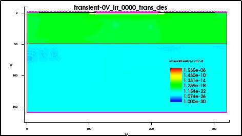

94 a b c d 72

 corresponding to 80 Frenkel pairs per micron in silicon.")
 evolution of the")
95 e f g Figure 3.16: TCAD simulation of the diffusion of the charge generated inside the silicon substrate by a Minimum Ionising Particle (MIP) corresponding to 80 Frenkel pairs per micron in silicon. a) Initial conditions with no event; b) generation of the charge at the moment of the event occurs; c-d-e-f-g) evolution of the charge diffusing toward the electrodes as a function of time 73
96 3.4.4 Radiation damage by 18 MV photon beam Figure 3.17 shows the average normalised response of the EPI diode after irradiation by a mixed photon-neutron field produced by an 18 MV medical LINAC. Detector samples were tested after pre-irradiation (4 Mrad in water) by a Co-60 source, and read out in passive mode. The decrease in response, and subsequently the CCE induced by irradiation, was less than 1.5%/300 Gy. This can be attributed to the generation of cluster defects in the EPI layer due to the presence of fast secondary neutrons inducing the creation of recombination centres with a very deep energy level in the silicon forbidden band gap (often attributed to the energy level E c ev) [123, 148, 167]. The measured reduction of the CCE in the radiation field from the 18 MV photon beam in the EPI diodes is comparable to other devices developed for medical applications [174, 175]. Figure 3.17: The response of the EPI diode as a function of the irradiation dose delivered by an 18 MV medical LINAC photon beam Note: Detector samples were tested after pre-irradiation (4 Mrad) on a Co-60 source. Each value represents the average response of 20 samples, and error bars were calculated as two times the SD of the average response measured by all the samples. 74
97 3.5 Conclusion This chapter examined the experimental measurements and numerical simulation techniques performed to characterise a new EPI diode developed at CMRP for dosimetry in EBRT, which demonstrated an unusual total dose radiation response. The developed EPI diodes demonstrated an increase in sensitivity with gamma irradiation in contrast to commercial diodes. Validation and fine-tuning of the simulation model were undertaken by comparing the simulated data with the electrical characteristics (I-V and C-V) of the device. The radiation hardness characterisation of the detector was performed by evaluation diode response using radiation fields from the Co-60 gamma source and 18 MV medical LINAC. The detectors showed a stable response within 5% for 120 kgy of the gamma irradiation dose (Co-60), following 40 kgy of pre-irradiation on a Co-60. The mechanism of radiation damage induced by the photon beam was studied via the simulation of the effect of the concentration of trapped charge in the S i /S i O 2 interfaces on the lateral extension of the depleted region when the detector operated in passive mode. The model developed fits the experimental data fairly well, and the main mechanisms of variation in the response of the device were explained by combining a CCE induced by the trapped charge at the S i /S i O 2 interfaces and by the radiation gettering effect. The effect of the radiation damage induced by photoneutrons generated in the 18 MV photon beam was quantified as 0.5%/100 Gy, demonstrating the high grade of radiation hardness of this new EPI diode, with a potential lifetime for standard clinical QA usage of approximately 70 cgy/week, or more than eight years. 75
98 CHAPTER 4: RADIATION HARDNESS FOR 2-D SILICON DIODE ARRAY (MP512) USED IN EBRT 4.1 Introduction The purpose of this study is to characterise an innovative silicon 2-D array detector for dosimetry in small field EBRT. In this chapter, single diode test structures are fabricated onto the same wafer for preliminary characterisation of the performance expected by the final prototype. This chapter also studies the basic electrical properties of I-V and C-V for the test structures and silicon 2-D array. The single test diodes are fabricated onto a set of p-type silicon substrates with three different p-stop implantation densities. The purpose of these tests is to determine the optimal configuration of the p+ top-implantation realised between the n+ diode junctions to minimise the crosstalk between pixels due to the generation of conductive channels between the sensitive elements. 4.2 Materials and methods MP512 array design and fabrication The MP512 is a monolithic pixel array of 512, 0.5 x 0.5 mm 2 ion-implanted diodes of on a bulk p-type 470 μm thick silicon substrate. The total array area is 52 x 52 mm 2, with 2 mm diode pitch. The silicon detector array is wire-bonded to a thin tissue-equivalent printed circuit board (PCB) and covered by a layer of protective epoxy to avoid accidental damage to the wire bonding. The PCB provides the fan-out for connecting the sensor to the readout electronics. The MP512 silicon detector operates in passive mode, with no bias voltage applied to the diodes. In this study, the MP512 detector was placed between two 5 mm thick PMMA slabs. The PMMA envelope of the detector served two purposes: (i) protecting from mechanical damages and (ii) shielding the sensor from ambient light [4]. Figure 4.1 shows a 76
 (left) and the MP512 detector mounted and wire-bonded to the thin PCB, with detector and wire bonding protected by a thin")

99 diagram of the detector embedded in the PMMA envelope (left) and an image of the detector mounted on the flexible PCB (right). Figure 4.1: Schematic of the M512 packaging between two PMMA slabs (not to scale) (left) and the MP512 detector mounted and wire-bonded to the thin PCB, with detector and wire bonding protected by a thin layer of epoxy resin (right) Two different substrates of the MP512 array are examined in this chapter. Every sample had its own number to distinguish between different implantation charge, different substrate manufacturer and resistivity. Table 4.1 illustrates the ion implantation and substrate resistivity of each device. Two sets of silicon substrates were examined one from a United States silicon provider (CMRP) and one from a European silicon facility (KDB). Table 4.1: Ion implantation and resistivity of two arrays Array sample number Ion implantation, p + Substrate resistivity and type µc 10 Ω-cm (CMRP substrate) µc 10 Ω-cm (KDB substrate) The ion implantation charge (µc) describes the total ion charges deposited in the substrate of the array to produce the p-stop junctions between the pixels of MP
100 The energy of the incident particles was 67 kev, which gave a 0.08 µm depth of penetration. The dopant concentrations available are summarised in Table 4.2. Table 4.2: Amount of dopant concentrations for the samples used in this thesis Name of the device + ion implantation Dopant concentrations Particles/cm 3 MP512 # 100 µc 7.74 x MP512 # 30 µc 2.32 x Test structure # 10 µc 7.74 x Test structures design and fabrication The test structures in this study were supplied by SPA-BIT in the Ukraine and manufactured on the same type of wafer as the detector array. These structures were very useful tools to verify the effect of changing the parameters of the production process on the performance of the single detector. The test structures were initially produced on the same p-type silicon substrate of 470 µm thick with a p + back junction (to realise the back ohmic contact), with a p + p-stop junction and n + diode junction. Single diode test structures were fabricated onto the same wafer for preliminary characterisation of the performance expected by the final prototype. Two configurations of the test structures are evaluated in this chapter. Figure 4.2 shows the first design with a guard ring, which was n + 5 μm in width and 5 μm from the edge of the anode. Figure 4.3 shows the second design of test structure, which was without a guard ring. The sensitive volume of the diode was 0.5 mm for each configuration. 78


101 Figure 4.2: Real and schematic diagram of the test structure with guard ring The test structures were placed on dual in-line (DIL) ceramic packages containing either six or eight diodes with a common back contact. A range of samples was examined, with different boron dopant implantation charges of 10, 30 and 100 μc. In addition, two different types of substrate were investigated: a 1 Ω-cm and 10 Ω-cm substrate from the CMRP foundry and a 10 Ω-cm substrate from the KDB foundry. The dopant implantation and substrates were grouped to determine which substrate and dopant implantation grouping was the best choice to use the silicon diode as a dosimeter in the clinical field. The data presented in this chapter were calculated as an average of all the diodes on a specific DIL ceramic package, for both the CMRP and KDB substrates. Figure 4.3: Real and schematic diagram of the test structure without guard ring 79
102 4.2.3 Readout system The readout system used to perform the measurements was the TERA system, which was discussed in Section I-V characteristics for test structure and MP512 Characterisation of the test structures and MP512 in terms of I-V allowed determination of the baseline signal by applying a reverse voltage bias through the diode. This signal or leakage current was produced by the diode in the absence of ionising radiation or light Experimental method I-V characteristics were determined using a Keithley 230 programmable voltage source to apply a bias through the diodes, and the current was measured using a Keithley 614 electrometer and Keithley 199 System DMM/scanner. These experiments evaluated two configurations of test structures with and without a guard ring. The MP512 full array was also tested via the same setup. The reverse voltage was applied to the diodes from 0 to -25 V, with an incremental step amplitude of -0.5 V, and the delay time was 1000 ms (between the application of the bias and current sampling to achieve the full stabilisation of the current). The test structure and MP512 were placed in a dark aluminium sealed container in order to protect the device from the photocurrent generation due to the ambient light and electromagnetic interference. The detectors were also kept at room temperature (approximately 295 K). For the test structure, the data points were acquired as an average of all the diodes on a particular DIL ceramic package, which all had the same geometry and substrate characteristics, with the substrate resistivity and pre-irrigation ion implantation 80
103 displayed on the plots. Uncertainties for all I-V plots were based on the 6.5 digit accuracy scale of the equipment used in this experiment. The scale of the instrument was variable, between a range of 20 pa to 200 na, and the uncertainties ranged from to 2 pa. The first I-V test was performed on the test structure diodes that did not have a guard ring. The test was also undertaken on different substrate resistivity and pre-irradiation dopant implantations. Figure 4.4 shows the diagram of the experiment, with the negative bias applied to the p + region and the ammeter connected to the n + region. In this experiment, the negative voltage was applied from 0 to -25V, with a step increment of -0.5 V. Figure 4.4: Schematic of the I-V test for test structure without guard ring The second I-V test was performed on the test structure diodes with the guard ring. The experiments were undertaken when the negative bias was applied to the p + region from 0 to -25 V with an increment of -0.5 V, and the ammeter was connected to the n + region of the diode pad. The guard rings in this test were either kept grounded (see Figure 4.5 left) or floating (see Figure 4.5 right). 81
104 Figure 4.5: Schematic of the I-V test for the test structure with a guard ring that is grounded (left) and floating (right) The third I-V experiment was undertaken on the MP512 full array. The negative bias was applied to the uniform p + region via one of the bias pins available on each side of the MP512 detector die, while the ammeter was connected to the n + region of each individual diode. The full array sample tested in this experiment was not equipped with a guard ring. The schematic of the test is shown in Figure 4.6. The voltage was set from 0 to -14 V with -0.5 V increments because the MP512 exhibited breakdown around -14 V, unlike the rest of the test structure, which was up to -25 V. Figure 4.6: Schematic of the I-V test for the MP512 array 82

105 The test of MP512 diodes was performed by selecting diodes in different positions across the array. Figure 4.7 shows the position of the detectors tested. The I-V characteristic was performed for both arrays of CMRP #21 and KDB #24. Due to having the same geometry in both arrays, the locations of the tested diodes were the same in both arrays. The idea behind testing the I-V of MP512 in different locations was to determine whether the geometry of the detector had any effect on the leakage current. Figure 4.7 shows the locations of the detectors tested. Figure 4.7: Locations of diodes tested on MP C-V characteristics As discussed in Section 3.3.2, the C-V characteristic is used to determine the depletion bias of detectors. The capacitance of the detector is also an important parameter to design the readout front end, which must tolerate the output equivalent capacitance presented by the detector at the preamplifier input. This is particularly important when the detector is used in passive mode, where the capacitance has its 83
106 maximum value. As for any real silicon detector, the C-V curve evaluation is not as simple as for an ideal p-n junction device as the one discussed in Chapter 3. This is due to the presence of multiple depletion steps that occur between the diode junction towards the lateral p-stop junction (only 10 μm apart) and towards the back ohmic contact of the substrate. Despite the difficult analysis of the experimental results, it is still important to measure the C-V characteristic of complex devices to define the alternating current small signal behaviour of the devices. The instrumentation (as described in Chapter 3) was the bridge capacitance meter Boonton This allows the application of positive and negative bias up to 100 V. For the test structures, this study measured the capacitance by applying a bias from 0 to -60 V, with -0.5 V increments, with the delay time set to 1000 ms. Using the same parameters and setup, three different configurations were tested: no guard ring, guard ring grounded and guard ring floating. The uncertainties for all C-V plots were dependent on the 3.5 digit accuracy scale of the machine. The scale used in the experiments was pf with two decimal places recorded, and the uncertainty for each data point presented was pf Radiation hardness characterisation Radiation hardness study by photons and photoneutrons for test structures In terms of radiation damage by photons, all test structures were irradiated up to 40 kgy water-equivalent dose, in steps of 10 kgy, as indicated in Table 4.3. Further, all test structures were exposed to the photoneutrons using a medical LINAC, which produced 18 MV. 84
107 Table 4.3: The dose received of each samples from test structures Sample Ion implantation μc Dose received-kgy 1 Ω-cm (CMRP) Ω-cm (CMRP) Ω-cm (CMRP) Ω-cm (CMRP) Ω-cm (CMRP) Ω-cm (KDB) Ω-cm (KDB) Ω-cm (KDB) Ω-cm (KDB) Ω-cm (KDB) Ω-cm (KDB) Photon damage experimental method After irradiation, the response of all test structures was measured at the Illawarra Cancer Care Centre of Wollongong Hospital using a Varian 2100C LINAC. This test evaluated the effect of irradiation by Co-60. The diodes were placed on top of the couch using a 30 x 30 cm 2 solid water phantom. The response of the detectors was performed by 6 MV x-rays at a dose of 100 MU with a dose rate of 600 MU/minute and a 20 x 20 cm 2 field size. The diodes were placed at an SSD of 100 cm and 1.5 cm depth in a water-equivalent phantom. The responses of all diodes before exposure to radiation were recorded, and a post-irradiation response was measured and normalised to the zero dose. All data acquisition was undertaken by the Rad-X Dose View acquisition system, as discussed in Section Photoneutron damage experimental method To assess the effect of photoneutrons on silicon detectors using a LINAC, the detectors were irradiated for a prolonged period with an 18 MV beam. The response was measured before any course of irradiation using 6 MV, as clarified earlier. This point was used as a reference against which the irradiated detectors could be compared and the response normalised. The response of the detectors was measured at the Saint George Care Hospital in Sydney using a Varian ix LINAC. The 85
108 irradiation of the detectors was performed via 18 MV x-rays at a dose of 9795 MU with a dose rate of 600 MU/minute and a 40 x 40 cm 2 field size. The diodes were placed at the surface of the phantom to avoid any thermalisation of the neutrons at an SSD of 90 cm, and placed at the surface of 130 mm of water-equivalent phantom as back-scatter material. This study used a field size larger than 10 x 10 cm 2 to produce the largest possible number of photoneutrons and reduce the exposure time. Due to using the large field size, the dose was increased to achieve an approximate equivalent dose of 300 Gy. A further test was performed with the test structure using the same parameters as above, except the detector was placed at d max of 18 MV within 30 x 30 cm 2 of a solid water phantom. Following this, the response of the detectors was investigated with the same conditions used to measure the response before irradiation Radiation hardness study by photons and photoneutrons for MP array (MP512) experimental method The same conditions adopted to test the test structures were used for the characterisation of two full array samples: MP512 sample #24 with 10 Ω-cm and 30 μc ion implantation KDB substrate, and MP512 sample #21 with 10 Ω-cm and 100 μc ion implantation CMRP substrate. The setup of the photon study is shown in Figure 4.8. The detectors were placed at an SSD of 100 cm, and placed at d max. In the top of the detector was 0.5 cm bolus, using 10 cm of water-equivalent phantom as back-scatter material. 86

109 Figure 4.8: The setup of the response test for the arrays 4.3 Results Electrical and I-V characteristics for test structure Figure 4.9 shows the I-V characteristics for the test structures without a guard ring, for both the CMRP and KDB substrates. All test structures expressed the predicted trend, which was an increase in leakage current with increased negative bias. This figure also exhibits a range of variation of slopes of the I-V results for the test structures, which differed from 15 to 125 pa at a maximum negative voltage of 25 V. Some detectors demonstrated a breakdown at voltage -25 V, while others had a leakage current lower than 100 pa. 87
110 Figure 4.9: I-V characteristics for all test structures without guard ring Figure 4.10 shows the I-V of the test structures with 1 Ω-cm CMRP substrate, with guard rings both floating and grounded. The sample with 10 μc shows that the floating guard ring did not have any effect on the leakage current, which was unexpected. Instead, the sample with 100 µc revealed a leakage current almost double when the guard ring was left floating, which showed that the geometry and structure of the guard ring was fully functioning, but required a steeper doping charge profile to be effective in such low resistivity substrate. The guard ring was an n+ junction 10 μm apart from the n+ junction of the pad diode. Between them, the p- stop junction must have at least 100 μc to avoid the guard ring, and the diode junctions were shorted by the electron channel generated by the induction of the positive charge trapped in the Si/SiO 2 interface. 88
111 According to Mishra et al. [176], detectors with a grounded guard ring show a lower leakage current than do those with a floating guard ring, which is in substantial agreement with the results obtained by the sample with 100 μc implantation charge. Figure 4.10: I-V characteristics for 1 Ω-cm CMRP substrate, showing different ion implantations with guard ring grounded and floating Figure 4.11 shows the I-V of the test structure with KDB substrate 10 Ω-cm, with a guard ring floating and grounded. The results obtained with the KDB substrate substantially confirmed the data obtained on the CMRP substrate to make the guard ring effective, a minimum charge of 100 μc is required. This is illustrated by the sample 100 μc in Figure 4.11, which showed a double leakage current at -20 V if the guard ring was not polarised. The sample of 10 μc and 30 μc showed no effect of polarisation of the guard ring on the leakage current, with an average value of the current higher at the same bias voltage as the 100 μc samples with the guard ring grounded. The results from the 100 µc KDB substrate were consistent with Mishra 89
112 et al. s results [176]. The results from the I-V of the CMRP substrate with 10 Ω-cm confirmed the results obtained for the other substrates. Figure 4.11: I-V characteristics for 10 Ωcm (KDB) substrate, different ion implantation with guard ring grounded and floating In conclusion, the guard ring structure had no effect if the p-stop implantation charge was lower than 100 μc, which limits options for manufacturing the full array. The use of a guard ring is also very problematic in a large number of channel arrays, and requires definition of extra contacts, which can be difficult in terms of routing the contacts. The characterisation by I-V convinced the researchers to avoid using a guard ring for a full array Electrical characterisation of MP512 full array Figure 4.12 shows the I-V characteristics for the diodes that were selected (as shown in Figure 4.7) for array sample #21 (CMRP substrate) and sample #24 (KDB 90
113 substrate). Due to the large extent of the leakage current at the breakdown, the logarithmic scale was applied to attain a better demonstration of the trend. Figure 4.12: I-V characteristics for both arrays from the MP512 CMRP and KDB substrates and same pixels are tested in both arrays in the positions of MP. MP with KDB substrate shows high leakage current compared to MP with CMRP substrate. Investigating the leakage current from the #21 array indicated that the trend for all diodes tested was consistent up to -12 V, where a sharp increase in leakage current occurred. Diodes #19, #123 and #257 showed the lowest leakage current, with a maximum current of 6, 18 and 33 pa, respectively. These were conspicuously lower than diode #243, which reached a maximum leakage current of 141 pa, and diode #8, which rose steadily to approximately 70 pa before a sharp increase at -12 V. From 0 to -12 V, the leakage current ranged from 1 to 100 pa for all diodes from the #21 array. Although this appeared to be a significant deviation, these results were comparatively far better than those demonstrated for the #24 array. 91
114 The leakage current observed for sample #24 of the KDB substrate exhibited more inconsistency than did sample #21. Fluctuating trends were observed with the diodes from array #24, and the breakdown was observed for all diodes at approximately -12 V. Diode #19 displayed a relatively constant leakage current, similar to the diodes from array #21; however, the current was significantly higher around 400 pa before breaking down at -12 V. With applied negative bias, the leakage current was increased for diodes #123 and #243. However, diode #243 showed a sharp increase of leakage current from -7 V. Similar behaviour was observed for diode #123, yet starting from -10 V. Both diodes showed breakdown at around -12 V. For diodes #8 and #257, the leakage current increased similarly to the previous diodes; however, the rate of increase was considerably higher. In terms of comparison between the two substrates, the lower leakage current was observed from sample #21 of the CMRP substrate with 10 Ω-cm resistivity. The KDB substrate nominally 10 Ω-cm, like the CMRP substrate showed larger leakage currents in the full array, with pixels consistently breaking down at approximately -12V. Therefore, the CMRP substrate device may be operated at a far greater negative voltage range than the KDB device. The test was performed for diodes from different positions on the array. Thus, the results from both arrays demonstrated that there was no clear relationship between leakage current and geometrical position. The results also showed that the manufacturing process could achieve good uniformity in terms of ion implantation across the entire four-inch wafer, where the detector array covered almost 40% of the area Capacitance characteristics (C-V) of test structures Figure 4.13 shows the C-V characteristics of the test structures of both substrates without a guard ring. All devices demonstrated the expected trend, which displayed a 92
115 maximum capacitance with no bias applied, and a quadratic reduction when a negative voltage was applied. Figure 4.13: C-V characteristics for the test structure of both substrates without a guard ring However, the two samples from 1 Ω-cm showed high capacitance and the response was relatively worse than for the 10 Ω-cm samples. The higher response of the capacitance was found for the sample with 1 Ω-cm, 30 μc ion implantation and approximately 88 pf at zero bias, which reduced to a minimum value of 31 pf at -25 V. In contrast, the sample from the same substrate (CMRP) with different ion implantation (100 μc) showed a better response for capacitance, with a maximum value of 44.7 pf at zero bias, and a reduction to 20 pf at -25. For both tested structures (CMRP and KDB), the 10 Ω-cm substrates demonstrated similar results and predictable trends. For the CMRP sample with 10 Ω-cm and 30 μc, the initial capacitance was 40 pf. For the KDB sample with the same resistivity and ion 93
116 implantation charge, the initial capacitance was 34 pf. Excluding these two samples, the remaining tested structures with all 10 Ω-cm substrates (both the CMRP and KDB) presented an initial capacitance from 28 to 34 pf. As the negative bias increased, all test structures with 10 Ω-cm substrate recorded a capacitance value from 10.5 to pf. In all cases, the results were in qualitative good agreement with the theory that relates the junction capacitance to doping concentration and bias applied by the following relationship: qε C j = 2(φ V a ) N an d N a +N d where φ is the built-in potential, V a is the bias applied, and N a and N d are the concentrations of the acceptor and donor dopants, respectively. The famous plot reported by Blankenship et al. [177] summarises the general trends and suggests a methodology to verify the data obtained experimentally see Figure
117 Figure 4.14: Silicon detector parameters monograph [177] Figure 4.15 shows the C-V characteristics of the sample of 1 Ω-cm CMRP substrate for different ion implantations with a guard ring. The guard ring in this assessment was tested as both grounded and floating. It was difficult to distinguish between the capacitance for a diode when the guard ring was grounded and floating; however, it was observed that the capacitance of the sample with 10 μc was considerably higher than the other samples with the same substrate and resistivity. 95
118 Figure 4.15: C-V characteristics for test structure 1 Ω-cm CMRP with guard ring Figure 4.16 shows the C-V characteristics of the sample of 10 Ω-cm CMRP substrate and different ion implantation with a guard ring. The guard ring in this assessment was tested as both grounded and floating. The plots indicate that the sample with 30 µc ion implantation showed a significantly lower capacitance than did the 10 and 100 µc samples. 96
119 Figure 4.16: C-V characteristics for test structure 10 Ω-cm CMRP with guard ring Figure 4.17 shows the C-V characteristics of the samples of 10 Ω-cm KDB substrate and different ion implantation with a guard ring. The guard ring in this assessment was tested as both grounded and floating. However, it was difficult to distinguish between the plots when grounded and floating. Despite this, the results indicated that the KDB substrate was more consistent than the CMRP substrate. 97
120 Figure 4.17: C-V characteristics for test structure 10 Ω-cm KDB with guard ring To conclude, with the exception of the test structures with 1 Ω-cm CMRP substrate shown in Figure 4.15, the difference between the capacitance of the other test structures was insignificant. In terms of the effect of doping concentration, this study observed a relationship between decreasing the capacitance for silicon and increasing the doping concentration [178] of the substrate. To conclude the effect of the guard ring on the capacitance of the silicon, there was little effect on the capacitance of the devices. The maximum deviation recorded between the floating and grounded guard ring for all substrates and different ion implantations was 1 pf. This represents a deviation of approximately 1 to 3% of the capacitance through all samples tested. Thus, the guard ring may have a slight influence on the noise in a readout system. 98
121 4.3.4 Radiation damage for test structures and MP Photon damage for test structure Figure 4.18 shows the relative response as a function of the accumulated dose for the test structures with 1 and 10 Ω-cm CMRP substrate and 10 Ω-cm KDB substrate with different ion implantation charges. All the samples showed a reduction of the response down to approximately 55% at 40 kgy, with a stabilisation between 30 and 40 kgy within 3%. All the plots trend were found to agree with previous works [142, 170]. Further, the KDB substrate suffered a larger decrease of response, and also showed a stabilisation between 30 and 40 kgy at 57%, which made it a good candidate to be selected for the final production of the full array. Figure 4.18: Relative response for test structures as a function of accumulated dose Photoneutron damage for test structure Figure 4.19 shows the relative response of a few samples of test structures decreasing, which were irradiated using 18 MV. The sample of 10 Ω-cm for the 99
122 CMRP substrate of both ion implantations charge showed consistent results and better performance than did the 10 Ω-cm KDB samples. The plot also indicates that the ion implantation affected the response of the detectors. For both substrates, the lower dopant concentration showed a significantly decreased response. Figure 4.19: Relative response for test structures as result of photoneutrons Further, the reduction in the response of the detectors was observed as a result of photon dose, while the decreased response was negligible due to the neutrons. Table 4.4: The relative response alterations due to the photoneutrons Sample Post-irradiation response (%) Error (%) 10 Ω-cm (CMRP) 10 μc Ω-cm (CMRP) 100 µc Ω-cm (CMRP) 100 μc Ω-cm (KDB) 10 μc Ω-cm (KDB) 30 μc Ω-cm (CMRP) 100 μc Table 4.4 indicates that the response of the sample of 10 Ω-cm with CMRP 100 µc exhibited a 1.4% drop, compared to a 14.4% drop for the sample with the same pre- 100
123 ion implantation, but a different substrate (KDB). Such low sensitivity to photoneutron radiation damage exhibited by the CMRP samples suggests a very short lifetime of the non-pre-irradiated material, which is a sign of a low quality silicon substrate. In the same manner, the sample of 10 Ω-cm KDB 10 µc demonstrated a large drop in response of 31.67%, in comparison to 3.16% for the CMRP substrate with the same pre-ion implantation. To conclude the damage by photons, the KDB sample results with 10 Ω-cm with different ion implantations charge were in good agreement with theory and the previous results obtained by Bruzzi et al. [142]. In contrast, the CMRP showed very unusual results for photoneutron irradiation, and the results again showed that the material has very poor quality and small reproducibility across the samples, with the error bars among samples exceeding 9%. To conclude the damage by 18 MV irradiation, the samples for the 10 Ω-cm CMRP substrate were less sensitive to radiation damage than the 10 Ω-cm KDB. The most important conclusion obtained from this test was of the effect of dopant implantation on response decrease. As specified previously, the greatest percentage decrease of response was observed with a sample with the lowest dopant concentration. The samples with high dopant concentration showed the smallest percentage decrease against radiation damage by photons. In conclusion, samples with 100 µc and 30 μc pre-irradiation ion implantation showed better performance than did samples with 10 μc ion implantation. This was because the higher doping concentration in the p+ junction helped produce a higher doping gradient between the junction and p-type substrate. This phenomenon caused a higher electric field through the junction, which extended the space charge region and CCE of the detector, especially when polarised in passive mode. 101
124 Photon damage for MP512 array The radiation damage test was performed on the MP512 arrays for both the CMRP and KDB substrates. Figures 4.20 and 4.21 show the relative response as a function of accumulated dose for array #24 (KDB) substrate, which had 10 Ω-cm and 30 µc, and sample #21(CMRP) substrate, which had 10 Ω-cm and 100 µc. The choice of these two specific arrays was based on the outcomes acquired from the test structures results in order to validate the best manufacturing configuration of substrate type and ion implantation charge. The sample with 10 μc ion implantation charge from the test structure did not show a positive result, which led the focus to the other samples with 30 and 100 μc. The test structure with the KDB substrate and 100 or 30 μc showed a large response resulting from high CCE, and demonstrated a comparatively lower sensitivity to radiation damage. Ideally, this study would have opted for the 100 µc ion implantation; however, due to technical issues during the manufacture process, this study opted for the 30 μc ion implantation for the KDB substrate, which is not far from the optimum. The CMRP substrate showed an overall low response; however, a very small sensitivity to radiation damage for both gamma and photoneutrons was observed. Thus, this study selected the sample with 30 µc ion implantation charge. 102
125 Figure 4.20: Relative response for MP512 sample #24 with KDB substrate at d max Figure 4.20 shows a significant relative response change between the responses before and after irradiation by Co-60 up to 10 kgy. The percentage difference of relative response from pre-irradiation to 10 kgy was approximately 31%. After being irradiated up to 40 kgy, the response stabilised at 20, 30 and 40 kgy with a difference between the responses of approximately ±4.5%, with fluctuations probably due to annealing effects related to the samples being stored at room temperature for long periods. 103
126 Figure 4.21: Relative response for MP512 sample #21 with CMRP substrate at d max Based on Figure 4.21, it is problematic to make any accurate assessment of the dose and relative response of the CMRP array. This large fluctuation of the response of the diodes was due to fluctuation of the baseline, which also produced large fluctuation in the absolute response. The lower sensitivity seems to be associated with the quality of the substrate, which was rich in the GRCs responsible for the lack of CCE. Sample #24 was found to be the sample most suitable to be used in the clinical characterisation performed during this study. 104
127 Figure 4.22: Comparison of the response of the test structures and MP512 full array as a function of accumulated dose The radiation hardness study performed on the test structures was confirmed by repeating the same test on an MP512 full array. This comparison was required to evaluate the effect of radiation damage on the cross talk between pixels, and the effect of distribution of the electric field on the response of the pixels, and also to establish the reproducibility of the experimental setup and manufacturing process. Figure 4.22 shows the comparison of the MP512 array and correspondent test diode. The deviation between the test structure and array response was less than 4.5% at 20 kgy, and less than 2.5% at 30 kgy, thereby confirming the validity of the method adopted Photoneutron damage for MP512 array Figure 4.23 shows the radiation damage after irradiation by photoneutron field for the MP with 30 µc for the KDB substrate. It shows that the decreased response was 105
128 less than 2.6%/300 Gy. This may refer to the generation of cluster defects in the Si- Oi 2 layer due to the creation of recombination centres [179]. Figure 4.23: A normalised response as a function of the irradiation dose using an 18 MV medical LINAC photon beam 4.4 Conclusion This study has tested the performance of silicon detectors in terms of their electrical characteristics and radiation hardness to determine the optimum substrate resistivity and pre-irradiation ion implantation for use in radiation therapy as a 2-D dosimeter. The I-V characteristic showed that there is no relationship between the amount of ion implantation and leakage current for test structures without a guard ring. Further, the I-V results indicated that, although a guard ring could help reduce the leakage current in a topology adopting at least 100 μc, it adds significant complexity to the architecture of a large 2-D array without a direct measurable benefit. This led this study to avoid using a guard ring in the final detector array design. The C-V results 106
129 indicated that there was a small influence on capacitance when using a guard ring in the test structures. The characterisation of the test structures indicated that the best performance in terms of radiation hardness can be achieved by generating a p-stop junction between the pixels with a boron concentration of 100 µc/cm 2. Even if the detector was unbiased, the presence of a strong boron concentration gradient mitigated the effect of reducing the carrier lifetime as the irradiation dose increased. The same conclusion could be reached by considering the effect of irradiation from photoneutrons generated by an 18 MV medical LINAC. The characterisation was performed on the test structures, and the methodology was confirmed by comparison with the measurement of the response of a full detector array, which agreed with the single diodes within 4%. In terms of comparing the test structure and MP array, this study indicated that the test structure response decreased less than the MP response. For the MP512 sample #21, the fluctuation of the response of the diodes was due to fluctuation of the baseline and the annealing effects. The results were obtained from the MP512 sample #24, which was supported by the simulation performed by Petasecca et al. [123]. The previous work was based on simulating an n+/p/p+ silicon structure with a TCAD radiation damage model for p-type substrates. Moreover, this study proved that a decreased CCE is associated with increased fluence. These results correlate with the data presented in Figure As a result, sample #24 of MP512 with 30 µc was used to determine the feasibility of the device for clinical use, especially for small field beams. The next chapter presents the experiments conducted related to dose linearity, uniformity, PDD, DPP, OF and beam profile. The MP512 was also used with a movable phantom to 107
130 characterise the beam profile in 2-D (X and Y) and to enable a comparison with EB3 film, which will be discussed in Chapter
131 CHAPTER 5: A TWO DIMENSIONAL SILICON DETECTORS ARRAY FOR QUALITY ACCURANCE IN SBRT MAGICPLATE Introduction The MP512 detector was pre-irradiated up to 40 kgy using a Co-60 gamma source to stabilise its response. Its radiation hardness performance was extensively characterised by irradiation with photons from a Co-60 gamma source, and on a mixed photoneutrons radiation field from 18 MV LINAC. This demonstrated very good radiation stability, with variation in response of approximately 1%/10 kgy (H 2 O) of Co-60 and 0.9%/10 kgy (H 2 O) on 18 MV LINAC. Therefore, based on the results obtained from the previous chapter, the silicon detector array of MP512 with 30 μc and KDB substrate was chosen. 5.2 Materials and methods MP detector array A description of the MP512 was presented in Section DAQ The DAQ system is an essential component of any multichannel detector device. The prototype of the MP512 DAQ system was custom designed by CMRP, based on a multichannel electrometer chip. The chip named AFE0064 (Texas Instruments) is a 64-channel current integrator that provides an analogue differential output proportional to the charge accumulated in a capacitor during a configurable, presettable timeframe for each channel. The chip is set electronically through a serial protocol interface on the lowest gain available to span the full scale up to 9.6 pc, with a resolution of 16 bit and a non-linearity of less than 0.1% [180]. Each current integrator is equipped with a double sampler for subtraction of the baseline a 109
132 feature that is particularly important when a high signal-to-noise ratio is required, as in medical instrumentation. The DAQ system uses eight chips, for a total of 512 channels that are readout in parallel by four analogue-to-digital (ADC) converters. The analogue front end and converters are handled by a field programmable gate array (FPGA) that provides the clocks and synchronisation circuitry to manage the trigger signal provided by the LINAC to synchronise the acquisition when the beam is on. A physical connection between the FPGA DAQ and LINAC is necessary by means of a coaxial cable. The FPGA also manages the USB 2.0 link with the host computer, where a graphical user interface (designed at CMRP for EBRT applications) provides real-time visualisation and all the commands necessary for the user to control the instrumentation. The DAQ system also allows asynchronous acquisition of the detector signals by generating an internal trigger with a frequency of up to 5 khz. It resolves and reports the amount of charge generated in each silicon detector/pixel for each LINAC pulse. This feature is unique and extremely important because it allows visualisation and quantitative analysis of the transient dose-rate effect of the radiation generated by the LINAC. For further details of the DAQ, refer to Fuduli et al. [181] Detector packaging characterisation Dosimetry is strongly affected by the scattering and attenuation of a given radiation field by the materials surrounding the sensitive volume of the detector. The MP512 was wire-bonded to a 0.5 mm thick flexible fibreglass PCB carrier. The detector and PCB carrier were designed to avoid using high Z contact pads, resulting in dose enhancement effect. The water equivalency on the MP512 was evaluated by placing the detector at a depth of 1.5 cm in a solid water phantom with 10 cm of backscattering material at an SSD of 100 cm, and irradiating the device with a 6 MV 110

133 photon beam of 10 x 10 cm 2 in size. The same measurement was repeated for the backside-irradiated detector. Figure 5.1 shows the setup of the experiments under LINAC. Figure 5.1: Schematic of the M512 packaging, inserting the MP512 upside down Uniformity The MP512 consisted of 512 pixels implanted on bulk p-type silicon substrate and connected to a readout of multichannel electronics. The response of a channel is the combination of the sensitivity of each pixel and the gain of its corresponding preamplifier channel, which can generally lead to small variations of the response from pixel to pixel. Typically, this issue can be addressed by an equalisation procedure, based on calculating a multiplication factor array, which can be used to equalise the response of the entire system, as reported earlier by Wong et al. [4]. The equalisation factor was obtained by irradiating the device at 100 cm SSD in a solid water phantom with a 20 x 20 cm 2 field of 6 MV energy photons at a depth of 10 cm. The setup of this test is shown in Figure 5.2. At a depth of 10 cm, the dose crossprofile of a LINAC equipped with flattening filter was considered flat and the response from the MP512 was recorded, generating the vector X i. Based on the hypothesis that the stimulus for all pixels is the same, the average response from all 111
134 channels (<X>) was calculated. The equalisation factor vector F i, and equalised detector response, X eq-i, were then: F i xi ; X x eq i xi F i (5.1) The uniformity of the array was calculated as a differential response from each pixel: X x x eq i eq (11,12) % 100 (5.2) xeq (11,12) where X eq (11,12) is the response of the central detector after the normalisation procedure described above, and can be visualised by a statistical histogram. Figure 5.2: Schematic of the equalisation setup Dose linearity measurement Ideally, the dosimeter should have a linear response with the delivered MUs. The linearity response of MP512 was verified by inserting the device into a solid water phantom with a size of 30 x 30 cm 2 at 1.5 cm depth and 10 cm of back-scattering material, at an SSD of 100 cm. The response to a 6 MV photon beam with field size 112
135 of 10 x 10 cm 2 was registered as a function of the total accumulated irradiation dose up to 500 cgy, with 50 cgy increments Percentage depth dose measurements The MP512 was inserted into a PMMA holder composed of a slab of 5 mm on the top and bottom of the detector. Sections of 30 x 30 cm 2 of solid water were used to provide the proper scattering conditions, with a slab 10 cm thick for the backscattering material and several slabs to obtain the depth dose profile from 1.5 to 30 cm depth. The device was irradiated with 100 MU by a field of 10 x 10 cm 2 at 100 cm SSD, by a 6 MV photon beam. The result was compared with measurements taken by a Markus IC (PTW-Freiburg, Germany) under the same experimental conditions (in solid water) Dose per pulse measurements The DPP dependence measurements were made for the range of to Gy/pulse. This was achieved using a field size of 10 x 10 cm 2 at 6 MV with a fixed dose rate of 600 MU/min, and changing the SSD and depth of the detector in a waterequivalent phantom. The DPP reference measurement was performed using IC CC13 at d max, and the response from MP512 was normalised to the chamber response ( Gy/pulse). Characterisation of DPP by changing the depth of the detector in a phantom can potentially be affected by variation in the response of the detector with the spectrum of the radiation. The measurement of percentage depth dose shows that MP512 is energy independent up to a depth of 25 cm. To determine the very low DPP, the depth was kept constant at 25 cm and the SSD was varied from 90 to 350 cm, as suggested by previous studies [182, 183]. 113
136 5.2.8 Beam profile measurement A beam profile of an x-ray photon beam is comprised of the inter-umbral regions (the region between two penumbral regions), penumbral regions (the region included between 20% and 80% of the maximum dose intensity) and out-of-field regions [97]. Both penumbra and output factor (OF) measurements were determined with the MP512 placed at a 10 cm depth in a solid water phantom at the isocentre. The square field size was collimated by the means of the jaws, ranging from 0.5 to 10 cm, keeping the MLC completely retracted in order to avoid the problems of interleaf and round leaf-end leakages that are typical for MLCs. The beam profile was evaluated using the central row of the detector array with 22 sampling points and a 2 mm pixel-to-pixel pitch. The alignment of the central pixel of the central row in respect to the beam was achieved by irradiating the detector with a 0.5 x 0.5 cm 2 beam, and moving the detector laterally relative to the beam with steps of 1 mm in both directions. The central position was identified when the corresponding detector pixel attained the maximum response. The measured data points for the profiles were calculated as the mean value of five repetitions, and the error bars of each data point were calculated as two SDs Beam profile measurements by EBT3 film Gafchromic EBT3 film (Ashland, Wayne, New Jersey) was used as the benchmark for the measurements of the beam profiles. The EBT3 films were cut into sections of 10 x 10 cm 2 and positioned at the centre of the solid water phantom at the isocentre. They were scanned with an A3 flatbed scanner (Epson Expression 10000XL). To ensure a proper scanner warm up and better film analysis consistency, each film was scanned six times and only the last three scans were kept to perform the analysis [184]. The films were scanned in 48-bit RGB colour mode with a scanning resolution 114
137 of 70 dpi (equivalent to a pixel size of mm); however, only the red channel was used for pixel-to-dose conversion, based on the calibration curve. Care was taken to scan the film in the same orientation at the centre region of the scanner to reduce scanner-induced non-uniformity [185]. The images were analysed using both the Image J Version 1.43U (National Institute of Health, United States) and MATLAB (The MathWorks Inc., Natick, Massachusetts) software tools. A set of calibration films was also prepared, exposed in the same experimental session and analysed following the same protocol. A 3 x 3 pixel 2-D median filter was applied to reduce image noise [184]. The data points located in the same position of the central row of MP512 were sampled for comparison of the profiles and calculation of the full width at half maximum (FWHM) of the beam. The error bar values for the film dosimetry measurements (not reported in the final plot for clarity) were determined from the uncertainty confidence limits resulting from the conversion of pixel value to dose by the optical density function: I O OD log 10( ) (5.3) I The intensity (I) and background intensity (I 0 ) values were measured from the image pixel values of the film scan with associated statistical errors, σ I and σ I0, respectively. SDs were calculated across three image datasets (repeated scans of the same film). The optical density was calculated from these intensity values and converted to dose in cgy via the dose calibration curve. A second-order polynomial function was fitted to the measured data of the dose calibration curve: 2 Dose A Bx Cx (5.4) 115
138 The polynomial function depends on associated fitting constants: A, B and C, with errors σ A, σ B and σ C, respectively. The SDs were determined statistically by repeating the fitting process across three film scan image sets. Thus, the final error (in cgy) in the calculated dose values from the EBT3 film measurements was dependent on the values and errors associated with the measured quantities of I and I 0, as well as the fitting constants of the second-order polynomial: 2 2 I0 I0 2C ln 2C ln 2 B I B I Dose 2 I 0 2 I A I0 ln10 I0 ln 10 I ln10 I ln 10 ( ) 2 2 I0 I0 log10 B log 10 c (5.5) I I 2 The average uncertainty calculated across all field size measurements was approximately ±1.9% OF measurements The OF was defined as the ratio of dose per MU at a specific field size to the reference field size [35]. The reference field size for this study was 10 x 10 cm 2, measured at the isocentre (10 cm in depth at an SSD of 90 cm) [35]. The OF was calculated by acquiring the response of the detector in the central pixel (row 11 and column 12) for a field size ranging from 0.5 x 0.5 to 30 x 30 cm 2. The measurement setup was the same as described in Section 2.8. The OF measured by MP512 was directly compared with the MOSkin a silicon MOSFET detector developed for skin dosimetry [95, 186]. MOSkin is a MOSFET with a water-equivalent depth measurement of 70 μm, which presents the advantage of a very small sensitive volume of approximately mm 3, and a minimal size of silicon die of approximately 0.5 mm 2. It is mounted in fully tissue-equivalent packaging, avoiding 116
139 wire bonding and high Z materials, thereby minimising the potential radiation field perturbation associated with OF measurements. The MOSkin measurements for OF determination were undertaken at the British Columbia Cancer Agency, Victoria, British Columbia, Canada. The American Association of Physicists in Medicine TG- 51 protocol was used by placing MOSkin at the isocentre in a solid water phantom (RMI Gammex) at a depth of 10 cm. A 6 MV photo beam was delivered from a Varian 21EX medical LINAC for this testing. The OF measurements taken by MP512, MOSkin and EBT3 films were also compared with several detector studies taken from the literature (Farmer ion chamber, Pinpoint ion chamber, Diamond PTW and Scanditronic diode unshielded) [187]. 5.3 Results Uniformity Figure 5.3 shows the uniformity statistics of the MP512 response after the equalisation factors were applied. Uniformity was evaluated considering two SDs from the mean value as small as 0.25% after equalisation was applied. Figure 5.3: Differential response of MP512 after equalisation 117
140 5.3.2 Dose linearity Figure 5.4 shows the dose linearity of MP512 for accumulated doses ranging from 50 to 500 MU, with 50 MU increments. The adjusted regression coefficient, R 2, was and vertical error bars were calculated by two SDs over five repetitions. From the slope of the linear fit, the conversion factor from counts to dose was counts/cgy, which corresponded to pc/cgy. Figure 5.4: Accumulated dose response of the central pixel Note: The solid line represents the linear fit Detector packaging Evaluation of the effect on dose measurement of packaging MP512 on a 500 μm thick flexible PCB was performed by irradiating the detector in the phantom in both face-up and face-down orientations. The relative difference in response of the MP512 in face-up and face-down was found to be +0.64% ± 0.1%. This showed that 118
141 the flexible thin PCB was a valid option for packaging a monolithic 2-D detector array Percent depth dose Figure 5.5 presents the PDD for MP512 measured in a solid water phantom in comparison to the PDD measured for the same radiation field with a Markus IC. The minimum depth of measurements was 5 mm water-equivalent depth (WED). The observed maximum difference between PDDs was approximately ±1%. Error bars were calculated as two SDs over five repetitions. Figure 5.5: PDD measured with MP512 of 6 MV photons and 10 x 10 cm 2 field in comparison with a Markus ion chamber Dose per pulse dependence Figure 5.6 shows the DPP response of the MP512, normalised to Gy/pulse, representing the response of the IC at d max (for a 6 MV photon beam with a field size of 10 x 10 cm 2 ). The error bars representing the uncertainties of the MP
142 measurements were two SDs. For each dose rate, the response of the MP512 was normalised to the dose measured by the IC placed next to the MP512. This assumed that the CC13 was dose-rate independent. The results obtained (maximum DPP dependence was approximately 5% in the whole range of dose rate evaluated) were in substantial agreement with the data measured by Zhu et al. [183] on commercially available single diodes for dosimetry in radiotherapy and manufactured on a p-type silicon substrate. Figure 5.6: DPP response for MP512 normalised to the DPP of 2.78 x 10⁻⁴ Gy/pulse Note: DPP was estimated at a depth of 1.5 cm and SSD of 100 cm. The x-axis represents the DPP in the order of 10-4 Gy/pulse Beam profile measurements Figure 5.7 shows the measurements of the beam profile for square beam sizes ranging from 0.5 to 5 cm. The plot compares the data measured by a set of EBT3 Gafchromic radiotherapy films (Ashland, Wayne, New Jersey) with the 120
143 measurements performed by the MP512. All MP512 profiles were normalised to the response of the central axis pixel (CAX) at row 11 and column 12, and aligned with the corresponding EBT3 profile to the value at 50% of CAX. Profiles for 5 x 5 and 10 x 10 cm 2 (Figure 5.7a and b) were aligned to the response of the CAX because the value at 50% was not available since the detector was too small for such field sizes (Figures 5.7a and b). The profile measured with EBT3 films was normalised to the average value of a 2 x 2 mm 2 area around the central axis of the beam profile. For a more accurate evaluation of the agreement between film and MP512, the datasets were analysed with MATLAB (MathWorks, Natick, Massachusetts) to generate a fit using the Curve Fitting Toolbox. The FWHM and penumbra (80%-20%) were evaluated by interpolating the data points using the interpolation shape preserving fit (with a resolution step of 0.01 mm), as summarised in Table 5.1. Table 5.1: EBT3 and MP512 FWHM and penumbra width (80%-20%) study for different Field size (mm) square field sizes at 10 cm depth and isocentre EBT3 MP512 MP512 EBT3 100 EBT3 FWHM (mm) Penumbra (mm) FWHM Penumbra ΔFWHM (%) Δ Penumbra (%) The MP512 and EBT3 films showed good agreement to within 1.36% in the evaluation of the FWHM of the field size. The MP512 gave penumbral widths (80%- 20%) that were nominally about 0.4 mm wider than those derived from the EBT3 film measurements. Additionally, the relative discrepancy increased with the decrease of the field size, suggesting an effect of averaging due to the size of the 121
144 detector sensitive area (0.5 x 0.5 mm 2 ). Also contributing was the effect of the detector pitch size (2 mm), which became too large relative to the steep gradients of the penumbra width, especially for very small field size beams. A detailed analysis of this effect was presented by Wong et al. [26]. However, the absolute value of the discrepancy was lower than 0.4 mm for the penumbra of the smallest field of 5 x 5 mm 2. Hence, the overestimation was acceptable for clinical use, considering that the general criterion for plan verification in small field therapies is approximately 1 mm distance to agreement. 122
145 (a) FS = 10 x 10 cm 2 (b) FS = 5 x 5 cm 2 123
146 (c) FS = 3 x 3 cm 2 (d) FS = 2 x 2 cm 2 124
147 (e) FS = 1 x 1 cm 2 (f) FS = 0.5 x 0.5 cm 2 Figure 5.7: Beam profiles measured with MP512 and EBT3 films for radiation fields ranging from 0.5 x 0.5 to 10 x 10 cm 2 Note: FS = field size. 125
148 5.3.7 OF measurements Figure 5.8 shows the response of the central diode of the MP512, MOSkin detector and EBT3 film as a function of the field size at the isocenter and at a depth of 10 cm for a 6 MV photon beam, normalised to the 10 x 10 cm 2 field size. For field sizes smaller than 1 x 1 cm 2, the MP512 over-responded (less than 4%); effect which has been observed earlier for point silicon diodes as well. This effect is due to perturbation of the radiation field by the silicon and the package material of the diode. With decreasing field size, the relative portion of the beam directly interacting with the silicon and surrounding materials of the packaging increased. This causes the electrons scattered from the silicon and packaging material take a more dominant role in the response of the detector. In contrast, the large field response was dominated primarily by electrons that were scattered from the solid water. By reducing the size of the nontissue equivalent detector and its packaging, this effect can be minimised. It almost disappears when a very small size point silicon detector, surrounded by no high Z materials such as the MOSkin is used to measure the OF. The MOSkin showed excellent agreement with the EBT3 films, having a response difference within 1.5%. The MOSkin s drop-in technology adopts only quasiwater equivalent materials, thereby minimising the effect of the dose enhancement of materials with a high atomic number. These results were compared with measurements taken by several research groups worldwide using commercial detectors in the same experimental conditions (Figure 5.9) [187]. Although this comparison involved measurements taken by different LINACs, it showed that the results obtained in this study fit very well with the trend obtained by very different detector types. Both the Farmer and Pinpoint ICs exhibited 126
149 a lower response when compared to other detectors due to the averaging effect of the sensitive volumes of 0.6 and 0.13 cm 3, respectively. For field sizes equal to 1 x 1 cm 2 and larger, the MP512 results agreed generally within 1%. It is possible to compensate for the over-response of the MP512 for these small field sizes using a small air gap above each pixel to ideally match the EBT3 film [188, 189]. Figure 5.8: Field size dependence response of MP512, MOSkin and EBT3 film normalised to response at 10 x 10 cm 2 field size Figure 5.9: Comparison of output factor for a different detector type and size from Sauer et al. [187] 127
150 5.4 Conclusion The MP512 is a 2-D array monolithic pixelated detector based on ion-implanted p- type silicon technology. It comprises 512 pixels arranged in a 22 x 22 array with seven extra elements for each detector side, covering an area of 52 x 52 mm 2. The sensitive volume of each diode is 0.5 x 0.5 x 0.1 mm 3, and the detector pitch is 2 mm. Variation of the response between the diodes in a flat field was ±0.25% after uniformity correction. Characterisation of the MP512 for phantom dosimetry QA in SRT applications was performed. PDD measurements of the MP512 were compared to those with ionising chambers and agreed to within 1.5% for depth. Dose rate dependence of the MP512 was evaluated by comparing the response to an ionising chamber. MP512 showed a DPP dependence within 1% down to Gy/pulse (approximately one order of magnitude lower than in-field DPP), while it showed approximately 5% at the lowest DPP of 0.9x10⁻⁵ Gy/pulse. The normalised beam profile distributions for square field sizes between 0.5 and 4 cm were measured with the MP512 and compared to Gafchromic EBT3 film. The MP512 showed excellent performance in beam profile reconstruction (FWHM discrepancy less than 1.3%). But in spite of much higher spatial resolution and pixel size of the available 2-D diode array, the MP512 produced a discrepancy in the penumbra of less than 0.4 mm for the smallest fields. This discrepancy still falls within the acceptance criteria of 1 mm generally accepted for small field dosimetry penumbra. A detailed comparison of the OFs and beam profiles measured by the EBT3 and MP512 showed that the MP512 is suitable for beam profile reconstruction down to a 10 mm square field size with a discrepancy of the relative response of the central channel of less than 2%. The MP512 showed an over-response (less than 4%) 128
151 with the 5 x 5 mm 2 field size because the scattering produced by the silicon surrounding the central pixel is not negligible. To prove this hypothesis, a single small silicon detector with tissue equivalent (TE) packaging (MOSkin) was tested and compared with the EBT3 film measurements. The MOSkin agreed to within 1.5% of the EBT3 film measurements down to a 5 mm field size. Further improvement of the MP512 for field sizes smaller than 10 x 10 mm 2 can be achieved by reducing the pixel pitch and pixel size down to 200 μm and introducing a small air gap above the detector to mitigate the dose enhancement produced by the silicon chip die. Before MP512 can be used as a patient-specific QA device, few more experiments should be undertaken to enable complete characterisation in a clinical scenario such as effect of MLC on dosimetry and characterisation of the energy dependence. Further, any 2-D detector array demonstrated angular dependence; however, no angular dependence study was performed. This is because we developed a new QA tool that allows the detector to be exposed perpendicularly to the beam. This was labelled a rotatable phantom, and is introduced in the next chapter. 129
152 CHAPTER 6: ROTATABLE PHANTOM FOR AUTOMATIC ALIGNMENT OF MP512 WITH THE LINAC BEAM 6.1 Introduction The rotatable phantom was designed and produced by CMRP to avoid the angular dependence of the detector. Inserting the MP512 in a rotatable cylindrical phantom that rotates synchronically with the gantry head of the LINAC helps the beam constantly incident perpendicularly to the detector. The design of such devices demands high accuracy and attention to detail. A 3-D computer-aided drawing package, SolidWorks (Dassault Systems SolidWorks Corporation, Massachusetts), was used to design the rotatable phantom model and technical drawings. 6.2 Rotatable phantom description The rotatable phantom was designed to have a cylindrical shape to allow the detector to rotate in an angular range of ±180, with a bidirectional accuracy position of ±0.25 degree. It can be rotated in a clockwise direction and its movement can be controlled either manually or automatically. The rotatable phantom angle can be determined using an inclinometer attached to the LINAC gantry head. The rotatable phantom was made from PMMA material (PMMA density 1.17 g/cm), which is close enough to tissue equivalent for 6 MV photon beam energy. The physical dimensions of the rotatable phantom are 30 cm diameter and 40 cm length, which approximately corresponds to the length of the thoracic duct of an adult. The rotatable phantom weight is 35 kg. The MP512 was held by thin PCB board and inserted into the phantom slot, which has a width of 13 cm and a depth of 15 cm. The MP512 was sandwiched between mm solid water slabs, and was placed on the centre of rotation. The solid water insert was necessary to accurately mimic the scattering conditions of water close to the detector in order to avoid the dose enhancement 130
153 generated by denser materials such as PMMA. At 6 and 10 MV, the maximum range of secondary electrons was approximately 15 and 25 mm, respectively. Using such an insert around the detector enables greater charge particle equilibrium (CPE) to be achieved. The rotatable phantom was synchronised with the LINAC by a stepper motor (NEMA 24) with a torque of 2.74 N-m. The motor was driven by the same acquisition system that managed the data collection of the detector signal. The stepper motor was placed on the large plate and attached with a small gear (the small gear has 18 teeth, while the large one has 64 teeth) that drove the large gear via a timing belt. The length of the timing belt was between 620 to 650 mm, and it had lateral flanges to avoid misalignment. The large gear was attached directly to the cylindrical phantom by the aluminium shaft (10 mm length). The position of the detector was monitored by an optical encoder (Absolute Encoder Multiturn ATM 60 SSI servo flange) attached at the phantom s shaft, and the LINAC head position was measured by an inclinometer placed on the accessory tray. This system of sensors was necessary to instantaneously maintain the alignment of the detector with the beam with discrepancy within ±1. The rotating encoder was used to determine the position of the phantom precisely with accuracy within a measuring step of degree. The digital interface used with the optical encoder was RS 422. Figure 6.1 (left) presents a drawing of the final design of the rotatable phantom by SolidWorks, while Figure 6.1 (right) presents a photograph of the phantom under the LINAC gantry. 131
 and actual rotatable cylindrical phantom with an inclinometer attached to the LINAC head (right) Inserting the MP512 in the")
154 Figure 6.1: Final design of the rotatable cylindrical phantom by SolidWorks (left) and actual rotatable cylindrical phantom with an inclinometer attached to the LINAC head (right) Inserting the MP512 in the rotatable cylindrical phantom that rotates synchronically with the gantry of the LINAC, helps to maintain the beam constantly perpendicular to the detector. Figure 6.2 shows the actual phantom following the LINAC gantry, with the beam constantly remaining perpendicular to the MP

155 Figure 6.2: Phantom with mechanical parts under the LINAC gantry 6.3 X-ray CT for rotatable cylindrical phantom Before dose is delivered to the patient, it is necessary to check the dose calculations of the treatment planning using a phantom. Such dose verification procedure is based on simulating the same plan calculated for the patient on the phantom geometry [190]. The next step involves measuring the dose by IC, semiconductors or films, then comparing it with the calculated dose. The rotatable phantom is used as a QA tool to verify the dose distribution. The rotatable phantom is scanned using CT simulation. CT simulation has the ability to provide accurate internal and external contour information for the phantom, converting CT numbers into electronic density of the different parts of the phantom. Figure 6.3 presents the CT image taken for the rotatable phantom in 3-D. The image clearly shows the solid water slabs (dark part, 133

156 MP insertion) that have density and CT number comparable to water (solid water density =1.02 g/cm, CT number =17). PMMA show higher CT numbers compared to water (CT number =133). Figure 6.3: CT image of the rotatable phantom in 3-D Based on the CT simulation, data were collected and used in the treatment planning system to simulate the proper radiation beams. Figure 6.4 shows the simulation of the incident beam by the treatment planning system on the rotatable phantom. Further testing of the accuracy of the dose distribution in the rotatable phantom compared to TPS calculations is not part of this work and will be analysed and reported by other students. 134
 a digital inclinometer placed on the")

157 Figure 6.4: 2-D isodose plan of the rotatable phantom 6.4 Mechanical and electronics parts of the rotatable phantom system The system is composed of three modules: (i) a digital inclinometer placed on the LINAC accessory tray, (ii) a rotating encoder attached at the phantom drum, and (iii) a slow-control module that includes the PMMA phantom equipped with a stepper motor and the power supply that provides all the power rails required by the system. Figure 6.5 presents a schematic representation of the rotatable phantom system. Figure 6.5: Schematic diagram of the rotatable phantom system 135
158 Note: The position synchroniser and DAQ of the analogue front-end electronics were embedded in the FPGA module, but are presented separately here for clarity. The inclinometer, optical encoder and slow control were the modules responsible for the active alignment of the detector, which was always kept perpendicular to the beam. The inclinometer is a commercial chip made by Analogue Devices. It is a 14- bit digital gyroscopic sensor that has a resolution of on the rotating angle. The FPGA controls the inclinometer with a Serial Peripheral Interface (SPI), and requests all information needed, such as the instantaneous position during normal operation, or parameters such as the power supply or the SPI status, in case it is operated in debugging mode [191]. The FPGA also manages the zeroing procedure for aligning the angle read by the inclinometer on the LINAC and by the encoder on the phantom, via using a simple command on the host computer s graphical user interface. The position of the inclinometer is used to make the rotation of the gantry compatible with the full range of the sensor, which is ±180. The slow control lies in the set of commands sent by the FPGA to control the stepper motor and read out the rotating optical encoder. The encoder is a multi-turn, 24-bit digital output, rotating sensor that adopts a RS-422 or SSI protocol [192] to communicate with the FPGA. The 12 most significant bits are dedicated to the number of revolutions and the 12 least significant bits are used to divide 360 into 4096 steps, giving a resolution of per step. The absolute position of the zero degree is set by sending a command from the host computer s graphical user interface, and this remains in the memory of the encoder unless changed by the user. A commercial stepper motor is used to rotate the phantom according to the information obtained from the inclinometer and encoder. The nominal resolution of the motor is 1.8 per step. The 136
159 stepper motor driver is a commercial microstep device called G203V from Gecko [193]. It is optically insulated to minimise the propagation of the noise. It divides each step of the motor by 10 to give a resolution of 0.18 per step. A system of gears and belt physically connects the motor to the phantom, allowing for a further increase in resolution by a factor of 3.34, which brings the effective rotating resolution of the phantom up to per step. 6.5 Slow control and DAQ digital design The main feature of the proposed rotatable phantom is the ability to detect the position of the gantry and activate the stepper motor to keep the detector perpendicular to the beam, based on numerical information from the inclinometer and encoder. The acquisition of inclinometer and encoder data is synchronised with the acquisition of the detectors so that each detector snapshot of the dose delivered in a frame also has information relative to the position of the LINAC head and the phantom. For the alignment of the phantom, the angle read from the inclinometer is compared to the angle read by the encoder and the absolute difference between the two data, scaled by the conversion factor given by the number of steps necessary to reach the desired position. Additional controls are added to determine the direction of the rotation of the motor, allowing for full bi-directional tracking of the gantry. Another constraint is related to the way the gantry moves: it spans all 360, from -180 to +180 ; however, it always returns to the position of 0 (crossing from the -180 to +180 position is not allowed). Controls guarantee that the phantom follows the same path. Figure 6.6 shows the firmware block diagram. 137
160 Figure 6.6: Simplified block diagram of the rotatable phantom architecture The difference between the angles recorded by the inclinometer and encoder also drives the frequency of the steps, which determines the speed of the motor to reach the final expected position. Many theories suggest that using a proportional-integralderivative (PID) control system is the optimal method for open loop control. Thus, a PID module was implemented in the FPGA firmware. A PID involves multiple calculations that remember past positions and generate an output that smoothly follows the behaviour of the input. In the proposed system, that means changing the frequency of the motor at each acquisition timing frame of 100 ms, 50 ms or even faster, depending on the application. An alternative solution was designed to avoid an overload of calculation called discrete angle control (DAC). The DAC approach simplifies the algorithm of the speed selection and allows for the use of a combinatorial network, instead of a complicated sequential arithmetic logic unit. The DAC approach appears to be very simple to implement; however, it can be slow to catch up with the gantry if the 138
161 LINAC accelerates because it has no memory of the previous position and relies on absolute error. A third solution, called Adaptive Discrete Angle Control (ADAC), has been designed in order to add some flexibility to the DAC mode. The ADAC approach checks the position s error and sets the initial speed of the motor in the same manner as the DAC mode; however, the last error estimation is remembered. As the system acquires again, the algorithm compares the new error with the previous error, and, even if the value falls in the same step, it increases or decreases the speed of a fixed amount in order to quickly track a speed variation of the gantry. 6.6 Experimental results: control system tuning and comparison at the workbench A test bench of the system was designed to verify the functioning of the three modules by internally generating the information about the position of the gantry moving at 2 /s to 7 /s. First, the PID was tuned using the Ziegel-Nichols method [194]. Figure 6.7 shows how the response of the system changes at different gains. At the minimum gain (K p = 1), the control was not fast enough to track the test signal, which simulated a continuous movement from 0 to 65 and backwards at the speed of 7 /s. Various values of the gain were used to attempt to reach the point of instability (K p = 50), then the three factors of the PID (K p, K i and K d ) were calculated following the Ziegel-Nichols equations. The optimised PID was then tested, and appeared to be fast enough to track the test signal and be stable. 139
162 Figure 6.7: PID tuning tracking mode To compare the performance of the three models by using an internal generated angle pattern (to simulate the data provided by the inclinometer), this study defined rising time, overshoot and settling time as per Figure 6.8 for the step response. Figure 6.8: Timing parameters 140
163 Figure 6.9 shows the response of the three control solutions (PID, DAC and ADAC) to a step of 90 (constant speed in one direction from -45 to +45 ). Looking at the timing performances summarised in Table 6.1, the ADAC method appears to have more performance control over the phantom. In particular, the step response has no overshoot a characteristic that is particularly relevant for the phantom due to its large mass inertia. Figure 6.9: Step response Table 6.1: Timing performances Step response DAC ADAC Optimised PID Rising 90% (s) Overshoot (deg) Settling time (s) Std tracking mode (deg) Std global (deg)
164 6.7 Experimental results using a medical LINAC The system was tested at the Illawarra Cancer Care Centre by using the Varian 2100EX Clinic and installing the inclinometer into the LINAC s accessory tray. As a preliminary test, the three control methods were compared using the same criteria evaluated in the test bench for the step response and for the tracking modality of operation. The speed of the gantry was calculated using the output of the inclinometer by the sampling rate, and ranged from 5.6 to 5.8 /s. The timing response of the three control systems was comparable with those calculated using the test bench; however, while the best performance was achieved using the ADAC method in the test bench, the DAC method had the best performance because of the lower speed of rotation of the gantry and the noise immunity of the DAC method (purely combinatorial with a Look-Up Table 6.2) to parasitic vibrations. In addition, higher uncertainties resulted from having the inclinometer mounted on the LINAC head. Table 6.2: Timing parameters in three modalities in clinical environment using a LINAC Step response DAC ADAC Optimised PID Rising 90% (s) Overshoot (deg) Settling time (s) Std global (deg) ± ± ± Conclusion The rotatable phantom as a QA tool for dose verification was designed by CMRP to overcome the angular dependence. The MP512 combined with the use of the rotatable phantom is a powerful tool, with real-time, accurate 2-D and potentially 3-D dose reconstruction capabilities for pre-treatment QA for SBRT and SRS verification. The rotatable phantom has the ability to rotate ±180 with accuracy by direction position within ±0.25. The residual angle due to the beam divergence over a 142
165 small field size (between 0.5 and 4 cm) was less than 1 and could be considered to have a negligible effect on the response of the pixels across the detector. 143
166 CHAPTER 7: A 2-D SILICON DETECTOR ARRAY (MP512) USED AS A TOOL TO STUDY MOVING TARGETS IN RADIOTHERAPY 7.1 Introduction The accuracy of the treatment in SBRT is proven to be affected by organ motion. It can be challenging to control tumours while minimising the dose of radiation delivered to healthy tissue during radiotherapy. Real-time DMLC tracking is the method used for intra-fraction motion management, which keeps healthy tissue away from the beam by tracking the tumour s movement. However, dose verification is required due to the presence of geometric and dosimetric uncertainties. In this study, a silicon detector array was used for the QA of a small field beam, such as in SBRT and SRS. In this study, the MP512 was used to reconstruct 2-D dose distributions of small field beams (1 x 1, 2 x 2 and 3 x 3 cm 2 ) in combination with a Calypso and DMLC tracking system. The 2-D dose distributions were performed using a movable platform called HexaMotion in the following scenarios: (i) without motion, (ii) with motion and (iii) with motion and DMLC tracking enabled. 7.2 Method and materials The detector system and packaging A 2-D silicon detector array MP512 was introduced in Section 4.2.1, while the readout system was discussed in Section When combining the MP512 detector with the Calypso system, there is a concern about the fluctuations of the signal baseline produced by electromagnetic field. This is because the induced current affects the detector cabling and electronic system. To resolve this problematic, radiofrequency (RF) aluminium shielding was designed. The aluminium sheet works as shielding box for the preamplifier boards, and the thickness was calculated to allow no more than 5% of RF to be transmitted through the aluminium sheet to the 144
167 electronic system. The next section presents the RF shielding calculations and shows the diagram of the detector in combination with the aluminium sheet and solid water Aluminium shielding calculation and simulations In this study, an aluminium shielding sheet was employed by being placed on top of the detector. The main advantage of using aluminium shielding is to attenuate the effect of the RF noise in the detector and electronic parts that are exposed to the Calypso system. The thickness of the aluminium used was approximately 2 mm, which reduced 95% of the initial intensity of the electromagnetic field. Table 7.1 presents the main electromagnetic parameters used to calculate the proper thickness. Table 7.1: Parameter values for calculating aluminium thickness Parameter Description Typ. value Units ε 0 Permittivity in free * F/m space μ 0 Permeability in free 4 π * 10-7 H/m space μ r Relative permeability 1 This value was obtained from [176] ω Oscillation 2 π *500 * 103 Hz σ Conductivity 3.54 * 104 (Ω cm)-1 The approximation of a plane-wave incident perpendicularly on the aluminium and the displacement current term of the Maxwell equation have the form: 2 i 2 r r r E E E z t t (6.1) ωε r ε 0 <<σ, 2 E = μμ z rσ E 2 t (6.2) The answer to the partial mixed derivative equation has the form of: E = E 0 exp( αz) exp i(ωt βz) (6.3) 145
168 where: β = α = μμ rσω 2 (6.4) The skin depth for the electromagnetic wave propagated by Calypso at a frequency of 500 khz is approximately: For an attenuation of 95%, this leads to: E 0 exp( z ) δ = 1 = 2 = 700 μm (6.5) α μμ r σω E 0 = 0.05 z 2 mm (6.6) where z refers to the aluminium thickness sheet which is 2 mm. Further, PMMA slabs and solid water were placed on top of the detector with the aluminium sheet, as shown in Figure 7.1. These layers were equivalent to 1.5 cm depth, which matched the d max for a 6 MV photon beam generated by the LINAC. This method was similarly used by Huang et al. in a single detector for entrance dosimetry, using covering metal (either aluminium or brass) to replicate the desired thickness corresponding to d max for energy ranges of MV photons [195]. 146

169 Figure 7.1: Schematic of the MP512 with PMMA, solid water and an aluminium sheet To verify the dose perturbation with the influence of the insertion of 2 mm of aluminium sheet on the top of the MP512 detector, the Monte Carlo Geant4 version 10.0p01 simulations were performed [196]. A 6 MV x-ray with square field beams of 1 x 1, 2 x 2 and 3 x 3 cm 2 were simulated when the x-ray passed through the solid water slabs of 30 x 30 x 30 cm 3. The simulation was based on replacing the 2 mm water with aluminium the reference simulation when the entire phantom is water. The aim of this simulation was replicated by placing the 2 mm aluminium sheet on top of the PMMA detector at an SSD of 100 cm. The beams were incident from phase space files formed by EGSnrc Monte Carlo, which models a Varian 2100C LINAC [197]. Standard physics packages were used for the simulation, which embraced Compton scattering and gamma conversion (photons), ionisation, photoelectric effect and position annihilation (leptons) and Bremsstrahlung. The physics parameter of particle range was fixed to 0.1 mm, while the maximum step length of electron/positron was set to 0.1 mm. The dose was counted inside the 147
170 phantom at a voxel resolution of 1 mm 3. Each simulation was fragmented into 10 parallel jobs each with unique seeds and the mean dose stated. Further, the uncertainties were evaluated by taking the SD across 10 simulations. For each field size, the 4 x 10 3 primary histories were simulated (primary histories refer to the number of electrons striking the x-ray target in the LINAC head). At a depth of 1.5 cm at the beam central axis (CAX) for each file size, the dose uncertainty was found to be approximately ±1% of the dose Baseline study The evaluation the efficiency of the aluminium sheet was measured by acquiring the baseline (leakage current) of the detector. The baseline measurements were performed with the following configurations: 1. with Calypso off 2. with Calypso activated and MP512 unshielded 3. with Calypso activated and the aluminium sheet placed on top of the phantom, as shown in Figure 7.1. To attain a large number of samples, acquisition of the baseline was performed to 120 seconds with a sampling rate of 360 Hz. Statistical analysis of the leakage current was measured and presented by calculating the average of the baseline and plotting the frequency distribution of its SD in each channel of MP512 in the three different configurations listed above Calypso four-dimensional (4-D) localisation system An important component in the experiment was the Calypso system provided by Varian, designed for radiotherapy and real-time target localisation in 4-D. The Calypso system can provide the most accurate and precise position of the target during treatment using transponders called beacons. The value of these beacons is 148

171 that they are not required to connect to the cable to track the object. The Calypso system consists of a 4-D electromagnetic array that can localise the beacon positions using RF. This array is placed above the beacons, then the 4-D electromagnetic array emits RF signals to excite the beacons, and each of these beacons has its own resonant frequencies. The electromagnetic array detects the signal from the beacons after being absorbed, and their positions are subsequently identified, as shown in Figure 7.2. The Calypso system can also display the position of the beacons in real time prior to the test beginning [60, 198]. Figure 7.2: Principle of electromagnetism with beacon in the Calypso system Note: In this study, the Z component was eliminated [199] Lung motion mimicking To study the performance of a silicon detector array with target movement, a real lung temporal pattern was used. This was extracted from a real patient s lung 149

172 movement recorded using a 4-D CT scan. A simplified version of the motion pattern was used with no vertical (Z) component of the movement. The pattern was a text file with absolute position frames between X and Y every 25 ms. The text file was uploaded to the HexaMotion platform. The motion was provided using the HexaMotion platform, which is discussed in the following section. Figure 7.3 shows the temporal pattern adopted for this test in X and Y directions. Figure 7.3: Lung trace motion in X (blue) and Y (green) coordinates HexaMotion six-dimensional (6-D) motion platform A 6-D motion platform (HexaMotion, ScandiDos, Uppsala, Sweden) was used in this study to mimic organ motion. The HexaMotion platform was manufactured as an accessory for Delta 4 and has the ability to simulate tumour motion in 6-D and read the position data from a text file. This study performed the motions in only two axes 150

173 (X and Y), following the lung temporal motion pattern described previously. The HexaMotion platform can be controlled from the treatment room using a software program. The platform was modified using a flat wood plate to carry the MP512 detector and DAQ system during the delivery of the beam, with the positioning accuracy of the platform being better than 0.5 mm. Figure 7.4 presents the experimental setup. Figure 7.4: Experimental setup of the MP512 carried by the HexaMotion platform Note: The flat wood plate of HexaMotion was adapted to support the detector, PMMA, solid water and aluminium sheet Experimental setup Dynamic wedge study The MP512 has the ability to measure pulse by pulse, which is very important for dose QA, especially in motion adaptive radiotherapy. Further, the MP512 has high temporal resolution in dose mapping and can be used to test and improve the performance of the feedback algorithm, which is used to drive the DMLC to track the 151

174 target movement measured by Calypso. To investigate the 3-D dose reconstruction (X, Y and t) of MP512, a dynamic wedge was tested. This wedge was combined with the lung motion pattern described in Section The dynamic wedge study was performed on a solid water slab positioned above the HexaMotion platform, testing three different scenarios. The wedge was tested using 6 MV beam energy with a total dose of 1000 MU and 600 MU/min. The MP512 was positioned at a depth of 1.5 cm and SAD of 100 cm. To avoid the effects of the angular response of the detector, the LINAC gantry was fixed perpendicularly Beam profile measurements using MP512 Beam profiles of 1 x 1, 2 x 2 and 3 x 3 cm 2 were performed in three scenarios: (i) no motion, (ii) motion without DMLC tracking and (iii) motion with DMLC tracking. The square field beams were collimated by the MLC, and jaws were retracted 1 cm in each direction, as shown in Figure 7.5. This was to minimise the end-of-lead leakage and permit the full range of movement in X and Y directions to 2 mm and 8 mm, respectively. Beam profiles were tested along the X and Y directions using the MP512 and EBT3 films. Both detectors irradiated with 6 MV, 1000 MU and a dose rate of 600 MU/min at a depth of 1.5 cm. They were aligned to an SAD of 100 cm. Figure 7.5: Diagram of jaws defining the square field size 152
175 For the no-motion study, the MP512 was placed on top of the movable phantom above the 6 cm of solid water as back-scatter material. A black cloth was used to cover the parts to protect the detector from ambient light. The beacons were positioned on the top and the Calypso system was activated as shown in Figure 7.6. For the motion study, a similar setup was used to the no-motion study, and the HexaMotion platform was operated based on the lung temporal pattern described in Section The Calypso system was activated, except without DMLC tracking enabled. The final study performed involved motion with DMLC tracking enabled. In this study, the MP was moved with the HexaMotion platform, and the Calypso system was activated. The beacon provided positional information related to cameras installed in the room that registered the position of the array relative to the coordinate system of the LINAC. This allowed localisation by the Calypso system. This position was then sent to DMLC tracking. In real time, the DMLC tracking software calculated the new positions of the MLC [200, 201]. All beam profiles of the MP512 were normalised to central pixel response (row 11, column 12) and aligned with the corresponding EBT3 profile to the value at 50% of the central pixel response. The responses of each detector (MP512 and EBT3 film) were calculated based on five repetitions of the same field. The error bars of each data point presented in the plot were calculated as two SDs. The MP512 was equalised using similar methods for MP-121, and the response variation across the whole detector was 0.5% [4]. 153
 positioned on the foam top of the detector and localised relative to the room coordinate system Note: The same setup was used for the three")
176 Figure 7.6: The final setup, showing the transponders (beacons) positioned on the foam top of the detector and localised relative to the room coordinate system Note: The same setup was used for the three different scenarios Beam profile measurements using EBT3 film Gafchromic EBT3 film was used as the benchmark for beam profile in the three different scenarios: no motion, motion without DMLC tracking and motion with DMLC tracking. The same procedures as in Section were used in this test to scan the film and calculate is response. 7.3 Results DAQ An important feature of the data acquisition of the MP512 is the graphical user interface, which provides a real-time visualisation of the charge collected by each pixel in a fixed integration time, as shown in Figure 7.7 (left). Additionally, the response of each single channel of the MP512 can be presented, as shown in Figure 154
 and investigation of the initial LINAC beam characteristics (right) 7.")
177 7.7 (right). All measurements were conducted with a delivery of 1000 MU to allow the LINAC beam to reach an appropriate stabilisation condition. Figure 7.7: Graphical user interface of the data acquisition (left) and investigation of the initial LINAC beam characteristics (right) D maps of MP512 The value of using MP512 is the ability to present the dose distribution in 2-D. Figure 7.8 shows the projected beam of different field sizes for three scenarios: (i) no motion, (ii) with motion and the tracking system disabled and (iii) with motion and the tracking system enabled. This study found that MLC leakage affects the dose distribution of a square plan for all field sizes. Moreover, visualisation of the effect of the motion indicated that the larger field size resulted in large dose redistribution. The LINAC output was confirmed to be the same for all configurations, regardless of the dose distribution across the detector. 155
 FS = 3 x 3 cm 2 Motion (i) FS = 3 x 3 cm 2 Motion + DMLC Figure 7.")
178 (a) FS = 1 x 1 cm 2 No motion (b) FS = 1 x 1 cm 2 Motion (c) FS = 1 x 1 cm 2 Motion + DMLC (d) FS = 2 x 2 cm 2 No motion (e) FS = 2 x 2 cm 2 Motion (f) FS = 2 x 2 cm 2 Motion + DMLC (g) FS = 3 x 3 cm 2 No motion (h) FS = 3 x 3 cm 2 Motion (i) FS = 3 x 3 cm 2 Motion + DMLC Figure 7.8: 2-D dose distribution at d max of MP512 for different field sizes in three cases Note: Pitch is 2 mm, X and Y axes present the channel numbers, and FS = field size. 156
179 7.4.1 Geant4 simulation of aluminium sheet effect and RF noise destruction performance Figure 7.9 shows the MP512 without shielding and the RF on, which is generated by Calypso. The baseline fluctuation measured up to 9% of the full signal scale during the beam delivery. This large fluctuation was estimated and showed a relatively small frequency count with a maximum of 25 occurrences (events/second) at 6%. Despite this, the fluctuation significantly affected the accuracy of the measurement. As a result, a stochastic current signal was produced that could not be distinguished from the signal generated by the beam. Further, this fluctuation affected the accuracy of the dose distribution in the out-of-field and penumbra areas. Using aluminium shielding completely removed the large amplitude fluctuation component, as shown by the blue bars in Figure 7.9. Figure 7.9: Baseline fluctuation distribution acquired with Calypso on (with and without aluminium sheet shielding blue and orange bars, respectively) compared to the baseline fluctuation with Calypso off (green bars) 157
180 Figure 7.10 (left) shows the results of the Monte Carlo simulation of the depth dose profiles for 1 x 1, 2 x 2 and 3 x 3 cm 2 field sizes. Further, the cross-profiles were presented at a depth of 1.5 cm, as shown in Figure 7.10 (right). Using 2 mm of aluminium sheet on top of the detector had a very small effect on the dosimetry. A minimum dose was decreased and can be show that in percentage depth dose measured by the central pixel of MP512 compared with IC beyond 14 mm depth. The simulation uncertainties were within 1%. In contrast, no substantial changes were exhibited in the cross-profiles for all field sizes. Further, there was an increase in the energy deposition in water in the first 14 mm build-up region due to the large amount of secondary electron fluence produced by aluminium compared to the same thickness of water equivalent material (aluminium density 2.7 g/cm 3 ). Figure 7.10: Comparison of the Geant4 simulations of present depth dose (left) and dose profile (right) for 1 x 1, 2 x 2 and 3 x 3 cm 2 field sizes with and without the aluminium sheet Note: The response was normalised to the central pixel response corresponding to the dose profile of a 3 x 3 cm 2 radiation field. 158
181 7.4.2 Dynamic wedge measurement Figure 7.11 shows the dose profile measured by MP512 for no motion, motion, and motion with DMLC tracking of the dynamic wedge. The difference between no motion and motion with DMLC not activated was estimated, and found to be an average of -18% along the wedge. Further, at the peak of +75% in the penumbra region, the displacement of dose distribution was found to be approximately 0.8 to 1 cm. The comparison between no motion and motion with DMLC tracking activated was that the integral response could rise to a maximum difference of approximately +15% in the region corresponding to the right side penumbra of the wedge, while keeping the disagreement with the no-motion scenario within -3% along the wedge. Figure 7.11: Dynamic wedge integral dose profiles taken in the central Y axis of MP512 (upper plot) and the percentage difference that normalised to the no-motion peak integral dose response (lower plot) 159
182 7.4.3 Beam profiles For the clinical lung motion pattern, the motion was generated by the HexaMotion platform, which included six movement axes following a patient-specific motion pattern. The motion pattern was provided by the Royal North Shore Hospital, Sydney. The pattern was simplified to 2-D motion in the X and Y directions, with the Z direction suppressed in order to diminish the effect of variation in the intensity of the beam due to changes in the SSD of the phantom. Figure 7.12 shows the dose profile measurements for different square field sizes (1 x 1, 2 x 2 and 3 x 3 cm 2 ) in the Y direction of the MP512 and EBT3 films for different sets (no motion, motion with DMLC tracking disabled, and motion with DMLC tracking enabled). All MP512 dose profiles were compared with EBT3 film. All MP512 dose profiles were normalised to the response of the central pixel (row 11, column 12). The EBT3 film dose profiles were normalised to the mean value of a 2 x 2 mm 2 area, which surrounded the central axis of the beam profile. Profiles measured by MP512 and EBT3 film were aligned to the value at 50% of CAX. The agreement between MP512 and EBT3 film was evaluated quantitatively using MATLAB (Mathworks Inc.) by creating a fit with the curve fitting toolbox. The penumbral width (80%-20%) was measured by interpolating the data points using the interpolation shape preserving fit. The FWHM and right hind side (RHS) penumbra width (80%-20%) calculations are shown in Table 7.2. The right side of the penumbra (80%-20%) displays the large distortion produced by the lung motion pattern. This was due to the offset of approximately 4 mm created by the motion in the +Y direction, which corresponded to the positive direction of the distance informed in Figure The results showed that the tracking technique can mitigate 160
183 the dose smearing due to the orange motion. The variation of the penumbra between the no-motion and motion was evaluated quantitatively to determine the efficiency, and found to be 2.4 mm. Further, this value was reduced down to 0.7 mm when the tracking was active. The comparison between the MP512 and EBT3 film showed that agreement was within 3% and 0.4 mm for the FWHM and penumbra width, respectively. a) b) c) 161
184 Figure 7.12: MP512 dose profile in different cases comparing the data measured by EBT3 for field sizes of (a) 3 x 3 cm 2, (b) 2 x 2 cm 2 and (c) 1 x 1 cm 2 in the Y direction Table 7.2: Summary of calculations of FWHM and RHS penumbra width (80%-20%) in the FS (cm 2 ) Y direction of all field sizes measured by MP512 and EBT3 film FWHM +/- 0.1(mm) Y direction EBT3 No motion Motion DMLC RHS Penumbra +/- 0.1(mm) FWHM +/- 0.1(mm) RHS Penumbra +/- 0.1(mm) FWHM +/- 0.1(mm) RHS Penumbra +/- 0.1(mm) 1 x x x MP512 No motion Motion DMLC FS (cm 2 ) FWHM +/- 0.1(mm) RHS Penumbra +/- 0.1(mm) FWHM +/- 0.1(mm) RHS Penumbra +/- 0.1(mm) FWHM +/- 0.1(mm) RHS Penumbra +/- 0.1(mm) 1 x x x Note: FS = field size. Figure 7.13 shows the profiles measured by MP512 compared with EBT3 film in the X direction. The lateral movement generated by the lung motion pattern in the X direction was approximately ±1 mm and the minimum leaf width in that direction was 2 mm. Therefore, when the tracking was activated, the leaf could not move more than 1 mm. Further, for all field sizes, it was observed that the beam profiles generated in case of motion were more comparable to the beam profiles when there was motion and DMLC tracking activated. This can be explained by the fact that the tracking system is not too sensitive in the X direction compared to the Y direction. The pattern of the beam profiles below 30% of the maximum dose was correlated to radiation leakage between the edges of closed leaves and did not exist in the profiles 162
185 measured in the Y direction. The FWHM and RHS penumbra width (80%-20%) calculations are shown in Table 7.3. a) b) c) 163
186 Figure 7.13: MP512 dose profile in different cases comparing the data measured by EBT3 for field sizes of (a) 3 x 3 cm 2, (b) 2 x 2 cm 2 and (c) 1 x 1 cm 2 in the X direction Table 7.3: Summary of calculations of FWHM and RHS penumbra width (80%-20%) in the FS (cm 2 ) X direction of all field sizes measured by MP512 and EBT3 film FWHM +/- 0.1(mm) X direction EBT3 No motion Motion DMLC RHS Penumbra +/- 0.1(mm) FWHM +/- 0.1(mm) RHS Penumbra +/- 0.1(mm) FWHM +/- 0.1(mm) RHS Penumbra +/- 0.1(mm) 1 x x x MP512 No motion Motion DMLC FS (cm 2 ) FWHM +/- 0.1(mm) RHS Penumbra +/- 0.1(mm) FWHM +/- 0.1(mm) RHS Penumbra +/- 0.1(mm) FWHM +/- 0.1(mm) RHS Penumbra +/- 0.1(mm) 1 x x x Note: FS = field size. 7.5 Penumbra width The penumbra width in a dose profile is defined as the distance between the 80% and 20% at d max. Figures 7.14 and 7.15 show the comparison of penumbra width (80 %- 20%) in the Y and X directions for a field size of 1 x 1 cm 2 (top), 2 x 2 cm 2 (middle) and 3 x 3 cm 2 (bottom). The penumbra agreement between MP512 and EBT3 film of Y and X was presented in Tables 7.2 and 7.3, respectively. 164
187 Figure 7.14: Comparison of penumbra width between MP512 and EBT3 film for field sizes 1 x 1, 2 x 2 and 3 x 3 cm 2 in the Y direction 165
188 Figure 7.15: Comparison of left hand profiles for 1 x 1, 2 x 2 and 3 x 3 field sizes along the X- direaction of EBT3 and MP512 measurments. Both the devices show the dose distribution generated by the leaf leakage with a minimal (within 2%) discrepancy 7.6 Conclusion The SBRT and SRS are widely used techniques for small field beam radiation therapy. Organ motion during the course of the treatment presents a challenge for clinicians. This issue has been taken into account by increased the PTV or using image guidance to shape the beam and intensity delivered to the movable targets, and by introducing DMLC tracking and 4-D Calypso systems. In response to this, an advanced QA system is required, especially with high spatial and temporal resolution. 166
189 The 2-D array MP512 was developed and tested with the Calypso system as a dose verification of moving targets in radiotherapy. The Calypso system is a 4-D localisation system based on real time that uses transponders (beacons) to localise the position of the object. The DMLC tracking system demonstrated the ability to account for target motion during treatment by performing measurements using the MP512. The MP512 results showed good agreement between the static and tracked measurements in terms of beam profile, and displayed a maximum difference of 2.8%. Supplied motion induced a spatial displacement component; however, this displacement was compensated for by the DMLC tracking system. The MP512 detector was proven to be an effective tool for pre-treatment verification of real-time adaptive deliveries with both high spatial resolution for dose profiling and high temporal resolution for pulse-by-pulse reconstruction. The MP512 has the ability to measure the dose in 2-D dose distribution, as shown for all field sizes. In comparison with EBT3 film, a discrepancy was found within 0.4 mm for FWHM and 4% for penumbra width. Using the HexaMotion platform with MP512 was successfully examined, with the motion of the HexaMotion platform provided via a lung motion pattern. The dose distribution measured by MP512 was compared with EBT3 film for no motion, motion, and motion with DMLC tracking system. The aluminium sheet with 2 mm thickness was introduced successfully on a surface of 10 mm thick solid water (2 mm aluminium + 10 mm solid water equivalent to d max for 6 MV) to minimise the baseline fluctuation due to the RF emitted by Calypso. Using the 2 mm aluminium sheet did not perturb the radiation field for any field size tested, as proven by Monte Carlo simulations. The PDD study with aluminium sheet showed agreement within 1% below d max in comparison to dose measured in water without using aluminium sheet. Using a 3-D lung motion pattern did not show any 167
190 effect on the detector response due to the ability of the design of the electronic readout system to minimise the noise. The MP512 has the ability to measure the dose in 2-D dose distribution, as shown for all field sizes. In comparison with EBT3 film, the discrepancy was found within 0.4 mm for FWHM and 4% for penumbra width. However, this study was performed only using one motion (lung motion pattern), and movement was restricted to the X and Y directions. Further, this study did not take into account the variation of the MP512 SSD from the LINAC source. Changing SSD leads to variation in the dose rate measured by the MP512 due to the presence of the motion in the Z direction. Further, this study used a fixed gantry position, rather than using the gantry as it is employed in real SBRT or SRS modalities. 168
191 CHAPTER 8: HIGH SPATIAL RESOLUTION MONOLITHIC SILICON ARRAY FOR STEREOTACTIC RADIOSURGERY 8.1 Introduction This chapter introduces a new silicon detector array named DUO512 that features a high spatial resolution and unusual geometry of sensitive volumes to those used in contemporary instrumentation in radiotherapy. This 2-D silicon detector array can be used in very small fields for stereotactic radiosurgery. The aim of this chapter is to investigate the effect of ionising radiation on DUO512. This chapter also presents the electric characteristics of the device for I-V and C-V. Moreover, the DUO512 s uniformity, dose linearity and reproducibility are presented, as well as the results of radiation damage studies using two modalities photons (by irradiation with a Co-60 source) and photoneutrons (by irradiation with 18 MV LINAC). 8.2 Materials and methods Design and fabrication The DUO512 is a monolithic dosimeter array that contains 512 microstrips of phosphorous ions implanted on a bulk p-type silicon KDB substrate and organised in a cross shaped topology. The total area of silicon is 52 x 52 mm 2, with a 200 μ-strip pitch. The sensitive area of the single strip is 20 x 800 μm 2, with a 100 μc p-stop implantation charge between each strip. The silicon detector array is covered by a thin layer of protective resin epoxy to avoid accidental damage to the connections. The board is not tissue equivalent, but is fibreglass (FR4) with a 500 μm thickness. The resistivity of the substrate is 10 Ω-cm and the substrate is 500 µm thick see Figure 8.1 (left). Figure 8.1 (right) shows the DUO512 assembled on the PCB carrier. 169


192 Figure 8.1: DUO512 pixel structure diagram (not to scale) (left) and DUO512 silicon detector array (right) Readout system The AFE readout system was employed to readout the current signal from the DUO512. The full description of this system was introduced in Section I-V characteristics The I-V characteristics were determined using a Keithley 230 programmable voltage source to apply a bias through the diodes. The current was measured with a Keithley 614 electrometer. The reverse voltage applied to the diodes ranged from 0 to -20 V, with an incremental step amplitude of -0.5 V. The delay time between the applied bias and current sampling to achieve the full stabilisation of the current was 1000 ms. The detector was placed in a dark sealed container to shield the device from photocurrent due to ambient light. All detectors were kept at room temperature (approximately 295 K). The I-V test of the DUO512 silicon array was performed by selecting diodes in different positions across the array. 170
Data Acquisition Systems design for Quality Assurance in advanced radiation dosimetry
 University of Wollongong Research Online University of Wollongong Thesis Collection 1954-2016 University of Wollongong Thesis Collections 2016 Data Acquisition Systems design for Quality Assurance in advanced
3D Diode Array Commissioning: Building Confidence in 3D QA Technology
 3D Diode Array Commissioning: Building Confidence in 3D QA Technology Caroline Yount, MS CANCER CENTER 3D QA The complex three-dimensional (3D) shapes of intensity modulated radiation therapy (IMRT) dose
Comparison of peripheral dose measurements using Ionization chamber and MOSFET detector
 ORIGINAL ARTICLES Comparison of peripheral dose measurements using Ionization chamber and MOSFET detector Gopiraj ANNAMALAI 1, Ramasubramanian VELAYUDHAM 2 ABSTRACT Received: 7.07.2009 Accepted: 2.11.2009
The Current State of EPID-Based Linear Accelerator Quality Assurance. Disclosures. Purpose of this First Talk 8/3/2017
 The Current State of EPID-Based Linear Accelerator Quality Assurance Timothy Ritter, PhD, DABR, FAAPM 1 Disclosures Employed by the Veterans Health Administration Faculty appointment with the University
Monica Kishore. Medical Physics Graduate Program Duke University. Approved: Jennifer O Daniel, Co-Supervisor. Fang-Fang Yin, Co-Supervisor
 Accuracy of Planar Dosimetry for Volumetric Modulated Arc Therapy Quality Assurance by Monica Kishore Medical Physics Graduate Program Duke University Date: Approved: Jennifer O Daniel, Co-Supervisor Fang-Fang
A Generalized Strategy for 3D Dose Verification of IMRT/VMAT Using EPID-measured Transit Images
 A Generalized Strategy for 3D Dose Verification of IMRT/VMAT Using EPID-measured Transit Images Aiping Ding, Bin Han, Lei Wang, Lei Xing Department of Radiation Oncology, Stanford University School of
Silicon Sensor Developments for the CMS Tracker Upgrade
 Silicon Sensor Developments for the CMS Tracker Upgrade on behalf of the CMS tracker collaboration University of Hamburg, Germany E-mail: Joachim.Erfle@desy.de CMS started a campaign to identify the future
SCINTILLATING FIBER DOSIMETER ARRAY
 SCINTILLATING FIBER DOSIMETER ARRAY FIELD OF THE INVENTION [0001] This invention relates generally to the field of dosimetry and, more particularly, to rapid, high-resolution dosimeters for advanced treatment
Commissioning. Basic machine performance MLC Dose rate control Gantry speed control End-to-end tests
 Acknowledgements David Shepard, Ph.D. Daliang Cao, Ph.D. Muhammad K. N. Afghan, Ph.D. Jinsong Ye, M.S. Tony P. Wong, Ph.D. Fan Chen, Ph.D. Min Rao, Ph.D. Vivek Mehta, M.D. Igor Gomola, Ph.D. David Housley
8/3/2016. The EPID Strikes Back. Novel Applications for Current EPID Technology. Joerg Rottmann, PhD. Disclosures and acknowledgements
 The EPID Strikes Back Joerg Rottmann Brigham and Women s Hospital / Dana-Farber Cancer Institute Harvard Medical School Disclosures and acknowledgements Disclosures Varian MRA grant Acknowledgements Boston
When small things matter. Small Field Dosimetry Application Guide
 R A D I AT I O N T H E R A P Y When small things matter. Small Field Dosimetry Application Guide Contents 1 Introduction 1 Introduction 2 2 The Physics of Small Fields 3 3 Detector Types 10 4 Detector
Commissioning and Calibrating a Linear Accelerator State-of-the-Art in 2010
 Commissioning and Calibrating a Linear Accelerator State-of-the-Art in 2010 Indra J. Das, PhD, FACR Department of Radiation Oncology Indiana University of School of Medicine & Midwest Proton Radiation
Characterisation of a cobalt-60 small-beam animal irradiator using a realtime silicon pixelated detector
 University of Wollongong Research Online Faculty of Engineering and Information Sciences - Papers: Part A Faculty of Engineering and Information Sciences 2016 Characterisation of a cobalt-60 small-beam
Four-dimensional in vivo dosimetry by dose reconstruction using continuous EPID images and phase sorting method. JiHyung Yoon.
 Four-dimensional in vivo dosimetry by dose reconstruction using continuous EPID images and phase sorting method Director of Dissertation: Dr. Jae Won Jung Major Department: Physics by JiHyung Yoon July,
Development of the Use of Amorphous Silicon (ASi) Electronic Portal Imaging Devices as a Physics Tool for Routine Linear Accelerator QA
 Electronic Portal Imaging Devices as a Physics Tool for Routine Linear Accelerator QA") Development of the Use of Amorphous Silicon (ASi) Electronic Portal Imaging Devices as a Physics Tool for Routine Linear Accelerator QA Gena M.A.H 1, Ahmed L.El-Attar 2, Elbadry M. Zahran 3, Hany El-Gamal
Development of the Use of Amorphous Silicon (ASi) Electronic Portal Imaging Devices as a Physics Tool for Routine Linear Accelerator QA Gena M.A.H 1, Ahmed L.El-Attar 2, Elbadry M. Zahran 3, Hany El-Gamal
ArcCHECK. The Ultimate 4D QA Solution. Your Most Valuable QA and Dosimetry Tools
 ArcCHECK The Ultimate 4D QA Solution A 4D isotropical cylindrical detector array for arc delivery QA and Dosimetry U.S.Patent No. 8,044,359; 6,125,335 Compatible with: FFF Beams VMAT RapidArc TomoTherapy
SRS MapCHECK. SRS Patient QA, No Film. Your Most Valuable QA and Dosimetry Tools
 SRS MapCHECK SRS Patient QA, No Film Your Most Valuable QA and Dosimetry Tools SRS Patient QA, No Film With improvements in targeting and localization, stereotactic treatments have become prevalent. To
PHYSICS QUESTIONNAIRE FORM
 PHYSICS QUESTIONNAIRE FORM Institution Name: Date: Contact Information (name, address, phone, fax, email): Physicist: Radiation Oncologist: Dosimetrist (if applicable): Study Coordinator (if applicable):
SUN NUCLEAR. EPIDose : An Overview of EPIDose and the EPIDose Process and Algorithm. corporation. Your Most Valuable QA and Dosimetry Tools
 EPIDose : An Overview of EPIDose and the EPIDose Process and Algorithm SUN NUCLEAR corporation Your Most Valuable QA and Dosimetry Tools introduction Pre-treatment dose QA is an important process required
Monte Carlo study on a new concept of a scanning photon beam system for IMRT
 NUKLEONIKA 2011;56(4):291 297 ORIGINAL PAPER Monte Carlo study on a new concept of a scanning photon beam system for IMRT Anna M. Wysocka-Rabin, Günter H. Hartmann Abstract. Intensity-modulated radiation
Beam Production, Characteristics and Shaping
 Beam Production, Characteristics and Shaping Dr. Manfred Sassowsky Outline X-ray production 60 Co units Linear Accelerators Beam characteristics Beam shaping Beam Production, Characteristics and Shaping
ArcCHECKTM. The Ultimate 4D QA Solution. Your Most Valuable QA and Dosimetry Tools. VMAT RapidArc TomoTherapy Pinnacle 3 SmartArc Conventional IMRT
 TM The Ultimate 4D QA Solution A 4D isotropical cylindrical detector array for arc delivery QA and Dosimetry U.S.Patent No. 8,044,359 What is? The world s first true 4D detector array The world s first
Improvements in dose calculation accuracy for small off-axis targets in high dose per fraction tomotherapy
 University of Wollongong Research Online Faculty of Engineering and Information Sciences - Papers: Part A Faculty of Engineering and Information Sciences 2012 Improvements in dose calculation accuracy
7/23/2014. Acknowledgements. Implementing a new digital medical accelerator. New Generation of Medical Accelerators
 Implementing a new digital medical accelerator John Wong Johns Hopkins University AAPM, Austin, 2014 Acknowledgements Yin Zhang, Ken Wang, Kai Ding (Commissioning - JHU) Esteban Velarde, Joe Moore (QA
IQM Detector Characteristics: Signal reproducibility
 The Integral Quality Monitor (IQM) System is a real-time beam verification system that monitors the accuracy of radiation delivery throughout each patient treatment without any user interaction. IQM continuously
University of Wollongong. Research Online
 University of Wollongong Research Online University of Wollongong Thesis Collection 1954-2016 University of Wollongong Thesis Collections 2013 Validation of a general model for Intensity Modulated Radiation
Semiconductor Detector Systems
 Semiconductor Detector Systems Helmuth Spieler Physics Division, Lawrence Berkeley National Laboratory OXFORD UNIVERSITY PRESS ix CONTENTS 1 Detector systems overview 1 1.1 Sensor 2 1.2 Preamplifier 3
CHAPTER 2 COMMISSIONING OF KILO-VOLTAGE CONE BEAM COMPUTED TOMOGRAPHY FOR IMAGE-GUIDED RADIOTHERAPY
 14 CHAPTER 2 COMMISSIONING OF KILO-VOLTAGE CONE BEAM COMPUTED TOMOGRAPHY FOR IMAGE-GUIDED RADIOTHERAPY 2.1 INTRODUCTION kv-cbct integrated with linear accelerators as a tool for IGRT, was developed to
Initial setup and subsequent temporal position monitoring using implanted RF transponders
 Initial setup and subsequent temporal position monitoring using implanted RF transponders James Balter, Ph.D. University of Michigan Has financial interest in Calypso Medical Technologies Acknowledgements
The Ultimate 4D QA Solution A 4D isotropic cylindrical detector array for arc delivery QA and Dosimetry.
 The Ultimate 4D QA Solution A 4D isotropic cylindrical detector array for arc delivery QA and Dosimetry. U.S.Patent No. 8,044,359; 6,125,335 Your Most Valuable QA and Dosimetry Tools 2 Y o u r M o s t
X-Tream: a novel dosimetry system for Synchrotron Microbeam Radiation Therapy
 University of Wollongong Research Online Faculty of Engineering and Information Sciences - Papers: Part A Faculty of Engineering and Information Sciences 2012 X-Tream: a novel dosimetry system for Synchrotron
Physical and dosimetric aspects of a multileaf collimation system used in the dynamic mode for implementing intensity modulated radiotherapy
 Physical and dosimetric aspects of a multileaf collimation system used in the dynamic mode for implementing intensity modulated radiotherapy Thomas LoSasso, a) Chen-Shou Chui, and C. Clifton Ling Department
BRANDON RICE UNIVERSITY OF FLORIDA
 METHODS FOR PRODUCING OFF-AXIS RATIO TABLES FROM MINI-MULTILEAF COLLIMATOR SHAPED CIRCULAR FIELDS FOR INPUT INTO A STEREOTACTIC RADIOSURGERY TREATMENT PLANNING SYSTEM By BRANDON RICE A THESIS PRESENTED
Evaluation of a diode array for QA measurements on a helical tomotherapy unit
 Evaluation of a diode array for QA measurements on a helical tomotherapy unit K. M. Langen, a S. L. Meeks, D. O. Poole, T. H. Wagner, T. R. Willoughby, O. A. Zeidan, and P. A. Kupelian Department of Radiation
Characterization, Commissioning and Evaluation of Delta 4 IMRT QA System. Ram Sadagopan 1 UTMD Anderson Cancer Center Houston, TX.
 Characterization, Commissioning and Evaluation of Delta 4 IMRT QA System Ram Sadagopan 1 UTMD Anderson Cancer Center Houston, TX. 1 Acknowledgements Collaborators: Jose Bencomo, Rafael. M. Landrove, Peter
8/3/2017. Use of EPIDs for Non-Routine Linac QA. Disclosure. Learning Objectives. Parts of this project received support from Varian Medical System.
 Use of EPIDs for Non-Routine Linac QA Bin Cai PhD Disclosure Parts of this project received support from Varian Medical System. Learning Objectives Learn the recent development of EPID based Non-routine
Accurate two-dimensional IMRT verification using a back-projection EPID dosimetry method
 Accurate two-dimensional IMRT verification using a back-projection EPID dosimetry method Markus Wendling, Robert J. W. Louwe, a Leah N. McDermott, Jan-Jakob Sonke, Marcel van Herk, and Ben J. Mijnheer
Simulation and test of 3D silicon radiation detectors
 Simulation and test of 3D silicon radiation detectors C.Fleta 1, D. Pennicard 1, R. Bates 1, C. Parkes 1, G. Pellegrini 2, M. Lozano 2, V. Wright 3, M. Boscardin 4, G.-F. Dalla Betta 4, C. Piemonte 4,
The evaluation of minimum detectable phantom thickness change using a scanning liquid filled ion chamber EPID dose response
 Iran. J. Radiat. Res., 2005; 3 (1): 3-10 The evaluation of minimum detectable phantom thickness change using a scanning liquid filled ion chamber EPID dose response M. Mohammadi 1,2,3* and E. Bezak 1,2
Post-irradiation colouration of Gafchromic EBT radiochromic film
 INSTITUTE OF PHYSICS PUBLISHING Phys. Med. Biol. 5 (25) N281 N285 PHYSICS IN MEDICINE AND BIOLOGY doi:1.188/31-9155/5/2/n4 NOTE Post-irradiation colouration of Gafchromic EBT radiochromic film Tsang Cheung
Characterization of an in vivo diode dosimetry system for clinical use
 Louisiana State University LSU Digital Commons LSU Master's Theses Graduate School 2002 Characterization of an in vivo diode dosimetry system for clinical use Kai Huang Louisiana State University and Agricultural
IMRT Delivery System QA. IMRT Dose Delivery. Acceptance testing. Why: specific tests for IMRT? Accuracy of leaf positioning (gaps) MLC Alignment
 MLC Alignment") 1 IMRT Delivery System Q Thomas LoSasso, PhD Memorial Sloan Kettering Cancer Center IMRT Dose Delivery cceptance testing Commissioning Quality assurance Verification Q Why: specific tests for IMRT? 2.
1 IMRT Delivery System Q Thomas LoSasso, PhD Memorial Sloan Kettering Cancer Center IMRT Dose Delivery cceptance testing Commissioning Quality assurance Verification Q Why: specific tests for IMRT? 2.
Mobius3D. Software based IMRT QA
 Mobius3D Software based IMRT QA What is Mobius Medical Systems? Clinical Expertise Software Expertise Nathan Childress, Ph.D., Founder Eli Stevens, Chief Technical Officer Support Expertise Physicists
A new approach to film dosimetry for high energy photon beams: Lateral scatter filtering
 A new approach to film dosimetry for high energy photon beams: Lateral scatter filtering Sandra E. Burch Department of Radiology, Medical College of Georgia, Augusta, Georgia 30912 Kimberlee J. Kearfott
Development of Double-sided Silcon microstrip Detector. D.H. Kah*, H. Park, H.J. Kim (BAERI JikLee (SNU) E. Won (Korea U)
 E. Won (Korea U)") Development of Double-sided Silcon microstrip Detector D.H. Kah*, H. Park, H.J. Kim (BAERI JikLee (SNU) E. Won (Korea U), KNU) 2005 APPI dhkah@belle.knu.ac.kr 1 1. Motivation 2. Introduction Contents 1.
Development of Double-sided Silcon microstrip Detector D.H. Kah*, H. Park, H.J. Kim (BAERI JikLee (SNU) E. Won (Korea U), KNU) 2005 APPI dhkah@belle.knu.ac.kr 1 1. Motivation 2. Introduction Contents 1.
Design and development of a silicon segmented detector for 2D dose measurements in radiotherapy
 Design and development of a silicon segmented detector for 2D dose measurements in radiotherapy David Menichelli, a,d,** Mara Bruzzi, b,d Marta Bucciolini, a,d Cinzia Talamonti, a,d Marta Casati, a,d Livia
SRS MapCHECK. SRS Patient QA, No Film. Your Most Valuable QA and Dosimetry Tools
 SRS MapCHECK SRS Patient QA, No Film Your Most Valuable QA and Dosimetry Tools SRS Patient QA, No Film As clinics strive to treat with the smallest field possible, the demand for SRS/SBRT QA grows as well.
The on-line detectors of the beam delivery system for the Centro Nazionale di Adroterapia Oncologica(CNAO)
") The on-line detectors of the beam delivery system for the Centro Nazionale di Adroterapia Oncologica(CNAO) A. Ansarinejad1,2, A. Attili1, F. Bourhaleb2,R. Cirio1,2,M. Donetti1,3, M. A. Garella1, S. Giordanengo1,
The on-line detectors of the beam delivery system for the Centro Nazionale di Adroterapia Oncologica(CNAO) A. Ansarinejad1,2, A. Attili1, F. Bourhaleb2,R. Cirio1,2,M. Donetti1,3, M. A. Garella1, S. Giordanengo1,
Muon detection in security applications and monolithic active pixel sensors
 Muon detection in security applications and monolithic active pixel sensors Tracking in particle physics Gaseous detectors Silicon strips Silicon pixels Monolithic active pixel sensors Cosmic Muon tomography
Comparison of measured Varian Clinac 21EX and TrueBeam accelerator electron field characteristics
 JOURNAL OF APPLIED CLINICAL MEDICAL PHYSICS, VOLUME 16, NUMBER 4, 2015 Comparison of measured Varian Clinac 21EX and TrueBeam accelerator electron field characteristics Samantha A.M. Lloyd, 1a Sergei Zavgorodni,
ASSESSMENT OF 2D AND 3D IMAGE CHARACTERISTICS OF AN OPTICAL CT SCANNER FOR 3D DOSIMETRY JARRAD BEGG B. APP. SCI. (APP. PHYS)
") ASSESSMENT OF 2D AND 3D IMAGE CHARACTERISTICS OF AN OPTICAL CT SCANNER FOR 3D DOSIMETRY JARRAD BEGG B. APP. SCI. (APP. PHYS) A THESIS SUBMITTED IN PARTIAL FULFILMENT OF THE REQUIREMENTS FOR THE DEGREE
ASSESSMENT OF 2D AND 3D IMAGE CHARACTERISTICS OF AN OPTICAL CT SCANNER FOR 3D DOSIMETRY JARRAD BEGG B. APP. SCI. (APP. PHYS) A THESIS SUBMITTED IN PARTIAL FULFILMENT OF THE REQUIREMENTS FOR THE DEGREE
Addressing Limitations of a Spatially Sensitive Large-Area Ion Chamber for Real-Time Verification of Intensity Modulated Radiation Therapy.
 Addressing Limitations of a Spatially Sensitive Large-Area Ion Chamber for Real-Time Verification of Intensity Modulated Radiation Therapy. by Xun Lin A thesis submitted in conformity with the requirements
Strip Detectors. Principal: Silicon strip detector. Ingrid--MariaGregor,SemiconductorsasParticleDetectors. metallization (Al) p +--strips
 p +--strips") Strip Detectors First detector devices using the lithographic capabilities of microelectronics First Silicon detectors -- > strip detectors Can be found in all high energy physics experiments of the last
Strip Detectors First detector devices using the lithographic capabilities of microelectronics First Silicon detectors -- > strip detectors Can be found in all high energy physics experiments of the last
Quality control of Gamma Camera. By Dr/ Ibrahim Elsayed Saad 242 NMT
 Quality control of Gamma Camera By Dr/ Ibrahim Elsayed Saad 242 NMT WHAT IS QUALITY? The quality of a practice is to fulfill the expectations and demands from: Patient Clinicain Your self Quality assurance
Evaluation of dosimetry parameters of photons and electron beams using a linear ionization chamber array
 Evaluation of dosimetry parameters of photons and electron beams using a linear ionization chamber array José A. Bencomo, * Geoffrey Ibbott, Seungsoo Lee, and Joao A. Borges Department of Radiation Physics.
Volumetric Modulated Arc Therapy. David Shepard Swedish Cancer Institute Seattle, WA
 Volumetric Modulated Arc Therapy David Shepard Swedish Cancer Institute Seattle, WA Disclaimer Our VMAT work has been sponsored in part by Elekta. Outline David Shepard VMAT Basics and VMAT Plan Quality
ArcCHECK, ein neuartiger QS-Ansatz bei der Rotationsbestrahlung
 ArcCHECK, ein neuartiger QS-Ansatz bei der Rotationsbestrahlung Treffen des Arbeitskreises IMRT der DGMP Würzburg, 26 + 27.03.2009 Salih Arican Sun Nuclear Corporation QA Challenge for Rotational Beams
Characterization and evaluation of an integrated quality monitoring system for online quality assurance of external beam radiation therapy
 Received: 5 January 1 Accepted: 1 September 1 DOI: 1.1/acm.11 RADIATION ONCOLOGY PHYSICS Characterization and evaluation of an integrated quality monitoring system for online quality assurance of external
Quality Assurance for the ATLAS Pixel Sensor
 Quality Assurance for the ATLAS Pixel Sensor 1st Workshop on Quality Assurance Issues in Silicon Detectors J. M. Klaiber-Lodewigs (Univ. Dortmund) for the ATLAS pixel collaboration Contents: - role of
Recent Technological Developments on LGAD and ilgad Detectors for Tracking and Timing Applications
 Recent Technological Developments on LGAD and ilgad Detectors for Tracking and Timing Applications G. Pellegrini 1, M. Baselga 1, M. Carulla 1, V. Fadeyev 2, P. Fernández-Martínez 1, M. Fernández García
An Introduction to TG-142 Imaging QA Using Standard Imaging Products. Mark Wiesmeyer, PhD, DABR Technical Product Manager Standard Imaging, Inc.
 An Introduction to TG-142 Imaging QA Using Standard Imaging Products Mark Wiesmeyer, PhD, DABR Technical Product Manager Standard Imaging, Inc. Goals Understand the nature and intent of TG 142 imaging
Introduction of a Single Chip TLD System for Patient Dosimetry
 Introduction of a Single Chip TLD System for Patient Dosimetry C. Hranitzky a, M. Halda a, G. Müller a, B. Obryk b, H. Stadtmann a* a Austrian Research Centers GmbH ARC, 2444 Seibersdorf, Austria. b Institute
A Guide to Radiochromic Film Dosimetry with EBT2 and EBT3
 A Guide to Radiochromic Film Dosimetry with EBT2 and EBT3 David F. Lewis Advanced Materials Group Ashland Specialty Ingredients Spain, April 2014 What is Radiochromic Film? A film that instantly changes
The HGTD: A SOI Power Diode for Timing Detection Applications
 The HGTD: A SOI Power Diode for Timing Detection Applications Work done in the framework of RD50 Collaboration (CERN) M. Carulla, D. Flores, S. Hidalgo, D. Quirion, G. Pellegrini IMB-CNM (CSIC), Spain
New fabrication and packaging technologies for CMOS pixel sensors: closing gap between hybrid and monolithic
 New fabrication and packaging technologies for CMOS pixel sensors: closing gap between hybrid and monolithic Outline Short history of MAPS development at IPHC Results from TowerJazz CIS test sensor Ultra-thin
- Water resistant. - Large size.
 GAFCHROMIC EBT product brochure GAFCHROMIC EBT FEATURES GAFCHROMIC EBT dosimetry film has been developed specifically to address the needs of the medical physicist and dosimetrist working in the radiotherapy
Analysis of Post-exposure Density Growth in Radiochromic Film with Respect to the Radiation Dose
 J. Radiat. Res., 53, 301 305 (2012) Analysis of Post-exposure Density Growth in Radiochromic Film with Respect to the Radiation Dose Katsumi SHIMA 1,2, Kunihiko TATEOKA 1 *, Yuichi SAITOH 1,2, Junji SUZUKI
Medical Imaging. X-rays, CT/CAT scans, Ultrasound, Magnetic Resonance Imaging
 Medical Imaging X-rays, CT/CAT scans, Ultrasound, Magnetic Resonance Imaging From: Physics for the IB Diploma Coursebook 6th Edition by Tsokos, Hoeben and Headlee And Higher Level Physics 2 nd Edition
Monolithic Pixel Sensors in SOI technology R&D activities at LBNL
 Monolithic Pixel Sensors in SOI technology R&D activities at LBNL Lawrence Berkeley National Laboratory M. Battaglia, L. Glesener (UC Berkeley & LBNL), D. Bisello, P. Giubilato (LBNL & INFN Padova), P.
Improved spatial resolution by MOSFET dosimetry of an x-ray microbeam
 University of Wollongong Research Online Faculty of Engineering - Papers (Archive) Faculty of Engineering and Information Sciences 2000 Improved spatial resolution by MOSFET dosimetry of an x-ray microbeam
Accuracy of rapid radiographic film calibration for intensity-modulated radiation therapy verification
 JOURNAL OF APPLIED CLINICAL MEDICAL PHYSICS, VOLUME 7, NUMBER 2, SPRING 2006 Accuracy of rapid radiographic film calibration for intensity-modulated radiation therapy verification Ravi Kulasekere, a Jean
Characterization of an in vivo diode dosimetry system for clinical use
 JOURNAL OF APPLIED CLINICAL MEDICAL PHYSICS, VOLUME 4, NUMBER 2, SPRING 2003 Characterization of an in vivo diode dosimetry system for clinical use Kai Huang, 1, * William S. Bice, Jr., 2, and Oscar Hidalgo-Salvatierra
DOSELAB TOMOTHERAPY TG-148 QA QUICK GUIDE TG-148 RECOMMENDED TESTS 1. V.B.1.C. - Y-JAW DIVERGENCE/BEAM CENTERING
 DOSELAB TOMOTHERAPY TG-148 QA QUICK GUIDE Rev. 1.0 DOSELAB TOMOTHERAPY TG-148 QA QUICK GUIDE DoseLab users may reference the following instructions to perform Tomotherapy Quality Assurance tests as recommended
Evaluation of the Radiation Tolerance of Several Generations of SiGe Heterojunction Bipolar Transistors Under Radiation Exposure
 1 Evaluation of the Radiation Tolerance of Several Generations of SiGe Heterojunction Bipolar Transistors Under Radiation Exposure J. Metcalfe, D. E. Dorfan, A. A. Grillo, A. Jones, F. Martinez-McKinney,
Effect of slit scan imaging techniques on image quality on radiotherapy electronic portal imaging
 The University of Toledo The University of Toledo Digital Repository Theses and Dissertations 2008 Effect of slit scan imaging techniques on image quality on radiotherapy electronic portal imaging Dean
Installation und Kommissionierung des Viewray MRIdian Linac Hamburg, 28. Mai 2018 Sebastian Klüter
 Installation und Kommissionierung des Viewray MRIdian Linac Hamburg, 28. Mai 2018 Sebastian Klüter MR-guided RT in Heidelberg Funded by the German Research Foundation (DFG) Heidelberg consortium received
CyberKnife Iris Beam QA using Fluence Divergence
 CyberKnife Iris Beam QA using Fluence Divergence Ronald Berg, Ph.D., Jesse McKay, M.S. and Brett Nelson, M.S. Erlanger Medical Center and Logos Systems, Scotts Valley, CA Introduction The CyberKnife radiosurgery
Fundamentals of Power Semiconductor Devices
 В. Jayant Baliga Fundamentals of Power Semiconductor Devices 4y Spri ringer Contents Preface vii Chapter 1 Introduction 1 1.1 Ideal and Typical Power Switching Waveforms 3 1.2 Ideal and Typical Power Device
GAFCHROMIC. Therapy Dosimetry Media Models to
 GAFCHROMIC Therapy Dosimetry Media Models 37-040 to 37-045! Superior uniformity and sensitivity! Dose rate and fractionation independent! Maps dose distribution! Provides quantitative measurements (via
Isocenter and Field of View Accuracy Measurement Software for Linear Accelerator
 Isocenter and Field of View Accuracy Measurement Software for Linear Accelerator Aleksei E. Zhdanov 1 and Leonid G. Dorosinskiy 1 Ural Federal University named after the first President of Russia B. N.
SUBCHAPTER 14. THERAPEUTIC INSTALLATIONS
 SUBCHAPTER 14. THERAPEUTIC INSTALLATIONS 7:28-14.1 Scope (a) This subchapter covers therapeutic installations used in the healing arts. These therapeutic installations include x-ray, accelerator and teletherapy
State of the Art Film Dosimetry
 State of the Art Film Dosimetry Micke A., Lewis D. Advanced Materials Ashland proprietary technology, patents pending Film Dosimetry Radiochromic Film EBT2/EBT3 One-Scan Protocol Multi-channel Film Dosimetry
Study of irradiated 3D detectors. University of Glasgow, Scotland. University of Glasgow, Scotland
 Department of Physics & Astronomy Experimental Particle Physics Group Kelvin Building, University of Glasgow Glasgow, G12 8QQ, Scotland Telephone: ++44 (0)141 339 8855 Fax: +44 (0)141 330 5881 GLAS-PPE/2002-20
ISPFILMQATM STATE-OF-THE-ART RADIOTHERAPY VERIFICATION SOFTWARE. Supports all major radiotherapy technologies! FilmQA TM
 FILMQA STATE-OF-THE-ART RADIOTHERAPY VERIFICATION SOFTWARE Supports all major radiotherapy technologies! FilmQA is optimized for use with Gafchromic film products, including EBT2 and RTQA2. FILMQA helps
Highly Miniaturised Radiation Monitor (HMRM) Status Report. Yulia Bogdanova, Nicola Guerrini, Ben Marsh, Simon Woodward, Rain Irshad
 Status Report. Yulia Bogdanova, Nicola Guerrini, Ben Marsh, Simon Woodward, Rain Irshad") Highly Miniaturised Radiation Monitor (HMRM) Status Report Yulia Bogdanova, Nicola Guerrini, Ben Marsh, Simon Woodward, Rain Irshad HMRM programme aim Aim of phase A/B: Develop a chip sized prototype radiation
Highly Miniaturised Radiation Monitor (HMRM) Status Report Yulia Bogdanova, Nicola Guerrini, Ben Marsh, Simon Woodward, Rain Irshad HMRM programme aim Aim of phase A/B: Develop a chip sized prototype radiation
Prototype electron phantom for radiographic and radiochromic film dosimetry
 Louisiana State University LSU Digital Commons LSU Master's Theses Graduate School 2010 Prototype electron phantom for radiographic and radiochromic film dosimetry Chad Joseph Robertson Louisiana State
Development of Solid-State Detector for X-ray Computed Tomography
 Proceedings of the Korea Nuclear Society Autumn Meeting Seoul, Korea, October 2001 Development of Solid-State Detector for X-ray Computed Tomography S.W Kwak 1), H.K Kim 1), Y. S Kim 1), S.C Jeon 1), G.
Sensitivity study of an automated system for daily patient QA using EPID exit dose images
 Received: 27 June 2017 Revised: 8 December 2017 Accepted: 27 January 2018 DOI: 10.1002/acm2.12303 RADIATION ONCOLOGY PHYSICS Sensitivity study of an automated system for daily patient QA using EPID exit
Designing an MR compatible Time of Flight PET Detector Floris Jansen, PhD, Chief Engineer GE Healthcare
 GE Healthcare Designing an MR compatible Time of Flight PET Detector Floris Jansen, PhD, Chief Engineer GE Healthcare There is excitement across the industry regarding the clinical potential of a hybrid
A positioning QA procedure for 2D/2D (kv/mv) and 3D/3D (CT/CBCT) image matching for radiotherapy patient setup
 and 3D/3D (CT/CBCT) image matching for radiotherapy patient setup") JOURNAL OF APPLIED CLINICAL MEDICAL PHYSICS, VOLUME 10, NUMBER 4, FALL 2009 A positioning QA procedure for 2D/2D (kv/mv) and 3D/3D (CT/CBCT) image matching for radiotherapy patient setup Huaiqun Guan,
JOURNAL OF APPLIED CLINICAL MEDICAL PHYSICS, VOLUME 10, NUMBER 4, FALL 2009 A positioning QA procedure for 2D/2D (kv/mv) and 3D/3D (CT/CBCT) image matching for radiotherapy patient setup Huaiqun Guan,
Development of Personal Dosimeter Using Electronic Dose Conversion Method
 Proceedings of the Korean Nuclear Spring Meeting Gyeong ju, Korea, May 2003 Development of Personal Dosimeter Using Electronic Dose Conversion Method Wanno Lee, Bong Jae Lee, and Chang Woo Lee Korea Atomic
Proton induced leakage current in CCDs
 Proton induced leakage current in CCDs David R. Smith* a, Andrew D. Holland a, Mark S. Robbins b, Richard M. Ambrosi a, Ian B. Hutchinson a a University of Leicester, Space Research Centre, University
Ludlum Medical Physics
 Ludlum Medical Physics Medical Imaging Radiology QA Test Tools NEW LUDLUM PRODUCT LINE Medical Physics Products Medical Physics Products What are they? Products used to measure radiation output and to
Charge Loss Between Contacts Of CdZnTe Pixel Detectors
 Charge Loss Between Contacts Of CdZnTe Pixel Detectors A. E. Bolotnikov 1, W. R. Cook, F. A. Harrison, A.-S. Wong, S. M. Schindler, A. C. Eichelberger Space Radiation Laboratory, California Institute of
Phantoms in Medical Physics (RT) U. Oelfke. Division of Radiotherapy & Imaging
 U. Oelfke. Division of Radiotherapy & Imaging") in partnership with Phantoms in Medical Physics (RT) U. Oelfke Division of Radiotherapy & Imaging uwe.oelfke@icr.ac.uk Making the discoveries that defeat cancer 1. Introduction What is a phantom? Wiki:
in partnership with Phantoms in Medical Physics (RT) U. Oelfke Division of Radiotherapy & Imaging uwe.oelfke@icr.ac.uk Making the discoveries that defeat cancer 1. Introduction What is a phantom? Wiki:
Aim. Images for this section: Page 2 of 13
 Changes in CT number of high atomic number materials with field of view when using an extended CT number to electron density curve and a metal artifact reduction reconstruction algorithm Poster No.: R-0094
Summer Student project report
 Summer Student project report Mika Väänänen September 1, 2017 Abstract In this report I give a brief overview of my activities during the summer student project. I worked on the scintillating fibre (SciFi)
Conflict Disclosure. Rotational IMRT. Arc therapy. Dynamic Arc therapy. Intensity Modulated Arc Therapy Principles and Perspectives
 Intensity Modulated Arc Therapy Principles and Perspectives Cedric Yu University of Maryland Conflict Disclosure Advisory Council on Advanced Treatment Delivery, Varian Medical Systems, Inc. Patent License:
QA Considerations. QA for LGK Perfexion : : Follow NRC licensing guidelines (10( CFR ) Leksell Gamma Knife Perfexion
 Leksell Gamma Knife Perfexion") Leksell Gamma Knife Perfexion QA Considerations Paula L. Petti, Ph.D. Taylor McAdam Bell Neuroscience Institute Washington Hospital Healthcare System Fremont, CA 1 QA for LGK Perfexion : : Follow NRC licensing
Leksell Gamma Knife Perfexion QA Considerations Paula L. Petti, Ph.D. Taylor McAdam Bell Neuroscience Institute Washington Hospital Healthcare System Fremont, CA 1 QA for LGK Perfexion : : Follow NRC licensing
3084 IEEE TRANSACTIONS ON NUCLEAR SCIENCE, VOL. 60, NO. 4, AUGUST 2013
 3084 IEEE TRANSACTIONS ON NUCLEAR SCIENCE, VOL. 60, NO. 4, AUGUST 2013 Dummy Gate-Assisted n-mosfet Layout for a Radiation-Tolerant Integrated Circuit Min Su Lee and Hee Chul Lee Abstract A dummy gate-assisted