16Mb LOW VOLTAGE, ULTRA LOW POWER PSEUDO CMOS STATIC RAM IS66WV1M16EALL IS66/67WV1M16EBLL DESCRIPTION. Features FUNCTIONAL BLOCK DIAGRAM JANUARY 2018
|
|
|
- Marybeth Phelps
- 5 years ago
- Views:
Transcription
1 IS66WV1M16EA IS66/67WV1M16EB 16Mb OW VOTAGE, JANUARY 2018 UTRA OW POWER PSEUDO CMOS STATIC RAM Features ighspeed access time : 70ns ( IS66WV1M16EA ) 60ns (IS66/67WV1M16EB ) CMOS ower Power Operation Single Power Supply VDD =1.7V~1.95V( IS66WV1M16EA ) VDD =2.5V~3.6V (IS66/67WV1M16EB ) Three State Outputs Data Control for Upper and ower bytes eadfree Available DESCRIPTION The ISSI IS66WV1M16EA and IS66/67WV1M16EB are highspeed,16m bit static RAMs organized as 1M words by 16 bits. It is fabricated using ISSI s high performance CMOS technology. This highly reliable process coupled with innovative circuit design techniques, yields highperformance and low power consumption devices. When is IG (deselected) or when CS2 is OW (deselected), the device assumes a standby mode at which the power dissipation can be reduced down with CMOS input levels. Easy memory expansion is provided by using Chip Enable and Output Enable inputs. The active OW Write Enable (WE#) controls both writing and reading of the memory. A data byte allows Upper Byte (UB#) and ower Byte (B#) access. The IS66WV1M16 EA and IS66/67WV1M16EB are packaged in the JEDEC standard 48ball mini BGA (6mm x 8mm). The device is also available for die sales. FUNCTIONA BOCK DIAGRAM A0~A19 VDD GND I/O0I/O7 ower Byte I/O8I/O15 Address Decode ogic I/O DATA CIRCUIT COUMN I/O 1M 16 DRAM Memory Array Upper Byte CS2 OE# WE# UB# B# Control ogic Copyright 2018 Integrated Silicon Solution, Inc. All rights reserved. ISSI reserves the right to make changes to this specification and its products at any time without notice. ISSI assu mes no liability arising out of the application oruse of any information, products or services described herein. Customers are advised to obtain the latest version of this device specification before relying on any published information and before placing orders for products. Integrated Silicon Solution, Inc. does not recommend the use of any of its products in life support applications where the failure or malfunction of the product can reasonably be expected to cause failure of the life support system or to significantly affect its safety or effectiveness. Products are not authorized for use in such applications unless Integrated Silicon Solution, Inc. receives written assurance to its satisfaction, that: a.) the risk of injury or damage has been minimized; b.) the user assume all such risks; and c.) potential liability of Integrated Silicon Solution, Inc is adequately protected under the circumstances SRAM@issi.com 1
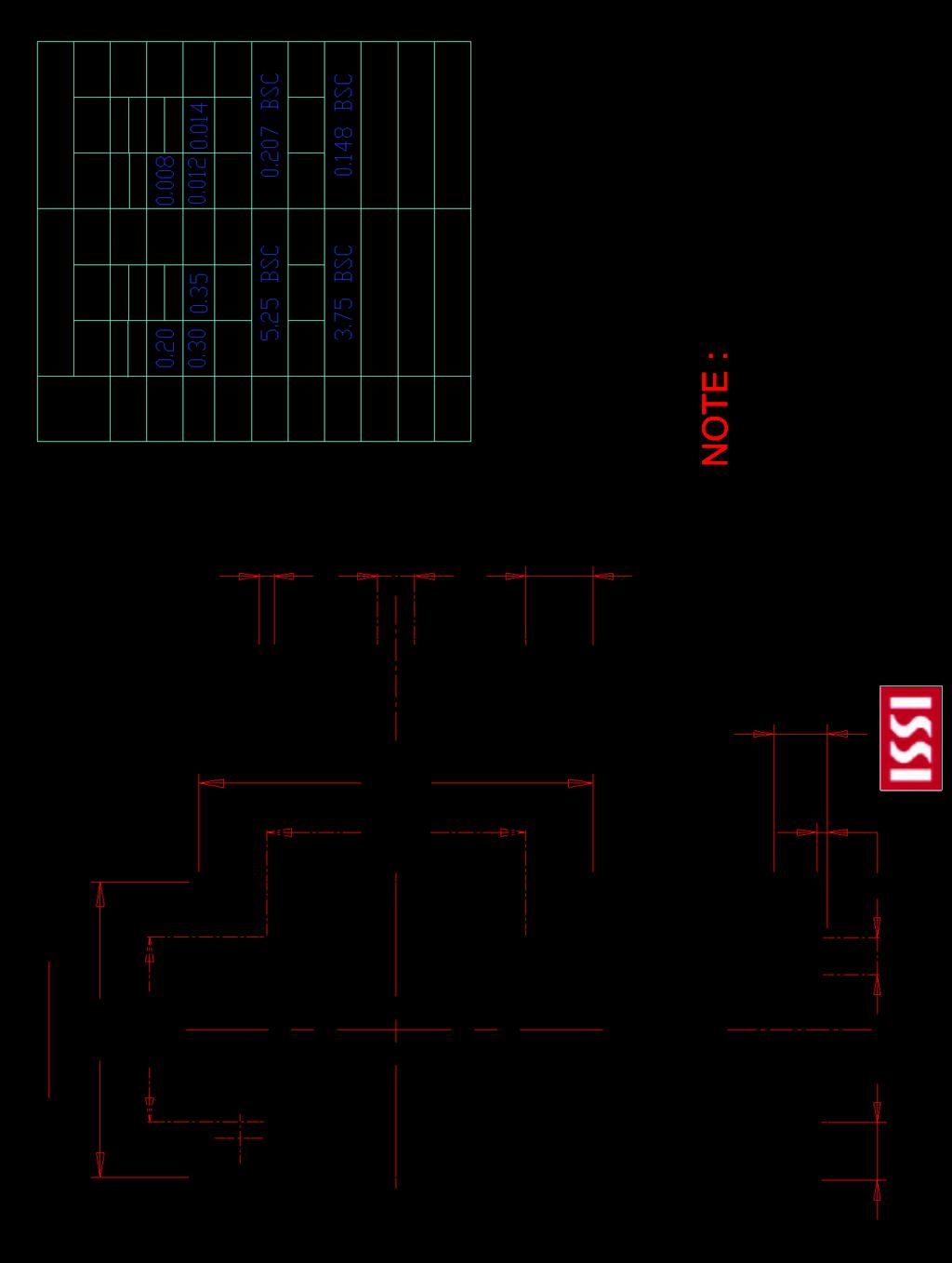
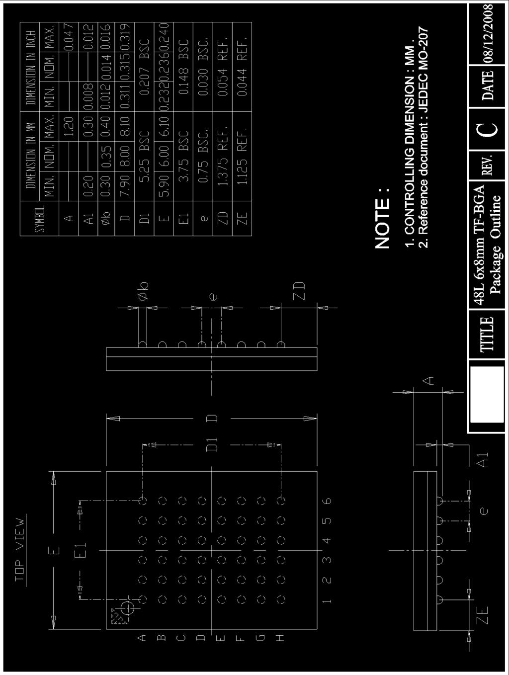
2 IS66WV1M16EA IS66/67WV1M16EB PIN CONFIGURATIONS 48Ball minibga (6mm x 8mm) Ball Assignment A B B# OE# A0 I/Q8 UB# A3 A1 A2 CS2 A4 I/Q0 C I/Q9 I/Q10 A5 A6 I/Q1 IQ2 D GND IQ11 A17 A7 I/Q3 VDD E VDD IQ12 NC A16 I/Q4 GND F I/Q14 I/Q13 A14 A15 I/Q5 I/Q6 G I/Q15 A19 A12 A13 WE# I/Q7 A18 A8 A9 A10 A11 NC Notes : 1. TSOP package option is under evaluation. PIN DESCRIPTIONS Symbol Type Description A0~A19 Input Address Inputs I/Q0~I/Q15 Input / Output Data Inputs/Outputs, CS2 Input Chip Enable OE# Input Output Enable WE# Input Write Enable UB# Input Upper Byte select B# Input ower Byte select VDD Power Supply Power GND Power Supply Ground SRAM@issi.com 2
3 IS66WV1M16EA IS66/67WV1M16EB POWER UP INITIAIZATION IS66WV1M16EA and IS66/67WV1M16EB include an onchip voltage sensor used to launch the powerup initialization process. When VDD reaches a stable level at or above the VDD (min) the device will require 50μs to complete its selfinitialization process. During the initialization period, should remain IG. When initializeation is complete, the device is ready for normal operation. VDD( min) 50 us 0V VDD Device Initialization Device for Normal Operation TRUT TABE Mode WE# CS2 OE# B# UB# I/O0 I/O7 I/O8 I/O15 VDD Current Not Selected ighz ighz ighz ighz ISB1,ISB2 ISB1,ISB2 Output Disabled ighz ighz ighz ighz Read DOUT ighz D OUT ighz D OUT D OUT Write Din ighz Din ighz Din Din OPERATING RANGE (VDD) Range Ambient Temperature IS66WV1M16EA (70ns) IS66WV1M16EB (55ns, 70ns) IS66WV1M16EB (55ns, 70ns) Industrial 40 C to +85 C 1.7V 1.95V 2.5V 3.6V motive, A1 40 C to +85 C 2.5V 3.6V motive, A2 40 C to +105 C 2.5V 3.6V SRAM@issi.com 3
4 IS66WV1M16EA IS66/67WV1M16EB ABSOUTE MAIMUM RATINGS Symbol Parameter Value Unit VTERM Terminal Voltage with Respect to GND 0.2 to VDD V TBIAS Temperature Under BIAS 40 to +85 C VDD VDD Related to GND 0.2 to +3.8 V TSTG Storage Temperature 65 to +150 C PT Power Dissipation 1.0 W Stresses greater than those listed may cause permanent damage to the device. This is a stress rating only, and functional operation of the device at these or any other conditions above those indicated in this specification is not implied. Exposure to absolute maximum rating conditions for extended periods may affect reliability. DC EECTRICA CARACTERISTICS (Over Operating Range) VDD = 2.5V3.6V (IS66/67WV1M16EB) Symbol Parameter Test Conditions VDD Min. Max. Unit VO Output IG Voltage Io = 1 ma V 2.2 V VO Output OW Voltage Io = 2.1 ma V 0.4 V VI Input IG Voltage(1) V 2.2 VDD V VI Input OW Voltage(1) V V II Input eakage GND VIN VDD 1 1 μa Io Output eakage GND VOUT VDD, Outputs Disabled 1 1 μa 1. VI (min.) = 2.0V AC (pulse width < 10ns). Not 100% tested. VI (max.) = VDD + 2.0V AC (pulse width < 10ns). Not 100% test DC EECTRICA CARACTERISTICS (Over Operating Range) VDD = 1.7V1.95V(IS66WV1M16EA) Symbol Parameter Test Conditions VDD Min. Max. Unit VO Output IG Voltage IO = 0.1 ma V 1.4 V VO Output Ow Voltage IO = 0.1 ma V 0.2 V VI Input IG Voltage(1) V 1.4 VDD V VI Input Ow Voltage(1) V V II Input eakage GND VIN VDD 1 1 μa Io Output eakage GND VOUT VDD, Outputs Disabled 1 1 μa 1. VI (min.) = 1.0V AC (pulse width < 10ns). Not 100% tested. VI (max.) = VDD + 1.0V AC (pulse width < 10ns). Not 100% test SRAM@issi.com 4
5 IS66WV1M16EA IS66/67WV1M16EB CAPACITANCE Symbol Description Conditions MIN MA Unit C IN Input Capacitance VIN = 0V 8 pf C IO Input/Output Capacitance (DQ) Vout = 0V 10 pf 1. Tested initially and after any design or process changes that may affect these parameters. AC TEST CONDITIONS Parameter 1.7V 1.95V ( Unit ) 2.5V 3.6V ( Unit ) Input Pulse evel 0.4V to VDD 0.2V 0.4V to VDD 0.3V Input Rise and Fall Time Input and Output Timing and Reference evel 5ns VREF 5ns VREF Output oad See Figures 1 and 2 See Figures 1 and 2 Symbol 1.7V 1.95V 2.5V 3.6V R1(Ω) R2(Ω) VREF 0.9V 1.4V VTM 1.8V 2.8V AC TEST OADS R1 R1 VTM VTM OUTPUT OUTPUT 30 pf Including Jig and scope R2 5 pf Including Jig and scope R2 Figure 1 Figure 2 SRAM@issi.com 5
6 IS66WV1M16EA IS66/67WV1M16EB 1.7V1.95V POWER SUPPY CARACTERISTICS (Over Operating Range) Symbol Parameter Conditions Device TYP. MA. 70ns Unit 1 ISB1 ISB2 VDD Dynamic Operating Supply Current Operating Supply Current TT Standby Current ( TT Inputs ) CMOS Standby Current ( CMOS Inputs ) VDD=Max.,IOUT=0mA, f=fma, All inputs = 0.4V or VDD 0.2V VDD=Max.,=0.2V, WE#= VDD 0.2V, f=1mz VDD=Max.,VIN=VI or VI, = VI, CS2=VI, f=1mz VDD=Max., > VDD 0.2V, CS2 < 0.2V, VIN > VDD 0.2V or VIN < 0.2V, f=0 1. At f = f MA, address and data inputs are cycling at the maximum frequency, f = 0 means no input lines change ma ma ma ua 2.5V3.6V POWER SUPPY CARACTERISTICS (Over Operating Range) Symbol Parameter Conditions Device TYP MA 55ns Unit VDD Dynamic Operating Supply Current VDD=Max.,IOUT=0mA, f=fma, All inputs = 0.4V or VDD 0.3V Typ.(2) ma 1 Operating Supply Current VDD=Max.,=0.2V, WE#= VDD 0.2V, f=1mz ma ISB1 TT Standby Current ( TT Inputs ) VDD=Max.,VIN=VI or VI, = VI, CS2=VI, f=1mz ma ISB2 CMOS Standby Current ( CMOS Inputs ) VDD=Max., > VDD 0.2V, CS2 < 0.2V, VIN > VDD 0.2V or VIN < 0.2V,f=0 Typ. (2) ua 1. At f = f MA, address and data inputs are cycling at the maximum frequency, f = 0 means no input lines change. 2. Typical values are measured at VDD = 3.0V, Ta = 25 ºC, and not 100% tested. SRAM@issi.com 6
7 IS66WV1M16EA IS66/67WV1M16EB READ CYCE SWITCING CARACTERISTICS (1) (Over Operating Range) Symbol Parameter Min Max Min Max Unit Notes t RC Read cycle time ns t AA Address Acess Time ns 1 t OA Output old Time ns t ACS1/ACS2 /CS2 Acess Time ns t DOE OE# Access Time ns 1 t ZOE OE# to ighz output ns 2 t ZOE OE# to owz output 5 5 ns 2 t CSM Maximum /CS2 pulse width us t ZCS1/ZCS2 /CS2 to ighz output ns 2 t ZCS1/ZCS2 /CS2 to owz output ns 2 t BA UB#/B# Acess Time ns 1 t ZB UB#/B# to ighz output ns 2 t ZB UB#/B# to owz output 0 0 ns 2 t CP IG (CS2 OW) time 5 5 ns 1. Test conditions and output loading are specified in the AC Test Conditions and AC Test oads (Figure 1) on page Tested with the load in Figure 2. Transition is measured ±100 mv from steadystate voltage. Not 100% tested. AC WAVEFORMS READ CYCE NO. 1 (1) (Address Controlled, OE#= VI, WE#=VI, UB# or B# = VI) Address trc tcsm CS2 toa taa toa DQ 015 PREVIOUS DATA VAID DATA VAID 1. WE# is IG for a Read Cycle. SRAM@issi.com 7
8 IS66WV1M16EA IS66/67WV1M16EB READ CYCE NO. 2 (1) (, CS2, OE# and UB#/B# Controlled) trc ADDRESS OE# taa tdoe toa tcsm tzoe tzoe tace1/tace2 CS2 tzcs1/ tzcs2 tcsm tzcs1/ tzcs2 UB#,B# tzb tba tzb DOUT IGZ DATA VAID 1. Address is valid prior to or coincident with OW (CS2 IG) transition, and is valid after or coincident with I G (CS2 OW) transition. SRAM@issi.com 8
9 IS66WV1M16EA IS66/67WV1M16EB WRITE CYCE SWITCING CARACTERISTICS (1) (Over Operating Range) Symbol Parameter Min Max Min Max Unit Notes t WC Write Cycle Time ns t SCS1/SCS2 /CS2 to Write End ns t CSM Maximum /CS2 pulse width us t AW Address Setup to Write Time ns t A Address old to End of Write 0 0 ns t SA Address Setup Time 0 0 ns t PWB UB#/B# Valid to End of Write ns t PWE WE# Pulse Width ns t SD Data Setup Time ns t ZWE WE# OW to ighz output ns 3 t ZWE WE# IG to owz output 5 5 ns 3 t CP IG (CS2 OW) time 5 5 ns 1. Test conditions and output loading are specified in the AC Test Conditions and AC Test oads (Figure 1) on page The internal write time is defined by the overlap of, UB#, B# and WE# OW, CS2 IG. All signals must be in valid states to initiate a Write, but anyone can go inactive to terminate Write. The Data Input Setup and old timing are referenced to the rising or falling edge of the signals that terminates the Write. 3. Tested with the load in Figure 2. Transition is measured ±100 mv from steadystate voltage. Not 100% tested. 4. tpwe > tzwe + tsd when OE# is OW. 5. Chip Select Active Time (both OW and CS2 IG) must not be longer than tcms of 15 us. SRAM@issi.com 9
10 IS66WV1M16EA IS66/67WV1M16EB AC WAVEFORMS WRITE CYCE NO. 1 (1) ( Controlled, OE#= IG or OW) twc ADDRESS CS2 WE# UB#,B# tcsm taw tpwe tpwb ta DOUT DIN tsa tzwe tzwe IGZ DATA UNDEFINED tsd td DATA IN VAID 1. Write address is valid prior to or coincident with OW (CS2 IG) transition, and is valid after or coincident with C S1# IG (CS2 OW) transition. WRITE CYCE NO. 2 (WE# Controlled, OE#= IG during Write Cycle) ADDRESS twc OE# tscs1 ta CS2 WE# taw tscs2 tpwe UB#,B# DOUT DIN tsa tzwe tzwe IGZ DATA UNDEFINED tsd td DATA IN VAID SRAM@issi.com 10
11 IS66WV1M16EA IS66/67WV1M16EB WRITE CYCE NO. 3 (WE# Controlled, OE#= OW during Write Cycle) twc ADDRESS OE# CS2 WE# OW taw tscs1 tscs2 tpwe ta UB#,B# tpwb DOUT DIN tsa tzwe tzwe IGZ DATA UNDEFINED tsd td DATAIN VAID WRITE CYCE NO. 4 (UB# / B# Controlled, CS2 is IG during Write Cycle) twc twc ADDRESS ADDRESS 1 ADDRESS 2 tcsm tsa WE# tpwb ta tsa tpwb ta UB#,B# WORD 1 WORD 2 DOUT tzwe DATA UNDEFINED IGZ tsd td tzwe DIN DATA IN VAID DATA IN VAID SRAM@issi.com 11
12 IS66WV1M16EA IS66/67WV1M16EB AVOIDABE TIMING and RECOMMENDATIONS Figure 3a : tcsm Violation 15us WE# Address Figure 3b : Recommendation 15 us 15us 5ns WE# Address SRAM@issi.com 12
13 IS66WV1M16EA IS66/67WV1M16EB AVOIDABE TIMING and RECOMMENDATIONS Figure 4a : tcsm Violation,WE# UB# &B# 15us Address Figure 4b : Recommendation 15us WE#, UB#, B# 15us Address 1. PSRAM uses DRAM cell which needs a REFRES action periodically to retain the information.this REFRES action is performed only when the device is not selected (Chip Select Pins are Disabled). A hidden REFRES action has to be executed by the device at least once every 15 μs of tcsm. 2. Figure 3a shows a timing example in which consecutive READ cycles for more than 15 us. This timing should be avoided for proper REFRES operation. REFRES operation can begin only during Chip Select pins are Disabled ( is igh and CS2 is ow ) for more than 5ns. Example on how to avoid tcsm violation in Figure 3a is shown in Figure 3b. 3. Figure 4a shows a timing example in which a single WRITE operation is maintained for a period greater than 15 μs. Since a proper REFRES action cannot be performed during device is selected by Chip Select pins, information stored in the device will not be retained if this timing occurs. Figure 4b is a timing example of using signal toggling for proper the WRITE operation SRAM@issi.com 13
14 IS66WV1M16EA IS66/67WV1M16EB IS66WV1M16EA Industrial Temperature Range: (40 o C to +85 o C) Voltage Range : 1.7V to 1.95V Config. Speed ( ns) Order Part No. Package 1Mx16 70 IS66WV1M16EA70BI mini BGA(6mm x 8mm), eadfree IS66WV1M16EB Industrial Temperature Range: (40 o C to +85 o C) Voltage Range : 2.5V to 3.6V Config. Speed (ns) Order Part No. Package 1Mx16 55 IS66WV1M16EB55BI mini BGA(6mm x 8mm), eadfree 70 IS66WV1M16EB70BI mini BGA(6mm x 8mm), eadfree motive (A1) Temperature Range: (40 o C to +85 o C) Voltage Range : 2.5V to 3.6V Config. Speed (ns) Order Part No. Package 1Mx16 55 IS67WV1M16EB55BA1 mini BGA(6mm x 8mm), eadfree 70 IS67WV1M16EB70BA1 mini BGA(6mm x 8mm), eadfree motive (A2) Temperature Range: (40 o C to +105 o C) Voltage Range : 2.5V to 3.6V Config. Speed (ns) Order Part No. Package 1Mx16 55 IS67WV1M16EB55BA2 mini BGA(6mm x 8mm), eadfree 70 IS67WV1M16EB70BA2 mini BGA(6mm x 8mm), eadfree SRAM@issi.com 14
15 IS66WV1M16EA IS66/67WV1M16EB 15
IS66WV51216DALL IS66/67WV51216DBLL
 8Mb LOW VOLTAGE, ULTRA LOW POWER PSEUDO CMOS STATIC RAM FEATURES High-speed access time: 70ns (IS66WV51216DALL, ) 55ns () CMOS low power operation Single power supply Vdd = 1.7V-1.95V (IS66WV51216DALL)
IS62WV25616DALL/DBLL, IS65WV25616DBLL 256K x 16 LOW VOLTAGE, ULTRA LOW POWER CMOS STATIC SRAM
 256K x 16 LOW VOLTAGE, ULTRA LOW POWER CMOS STATIC SRAM FEATURES High-speed access time: 35, 45, 55 ns CMOS low power operation 30 mw (typical) operating 6 µw (typical) CMOS standby TTL compatible interface
IS62C51216AL IS65C51216AL
 IS62C51216AL IS65C51216AL 512K x 16 LOW VOLTAGE, ULTRA LOW POWER CMOS STATIC RAM FEATURES High-speed access time: 45ns, 55ns CMOS low power operation 36 mw (typical) operating 12 µw (typical) CMOS standby
IS61WV3216DALL/DALS IS61WV3216DBLL/DBLS IS64WV3216DBLL/DBLS
 IS61WV3216DALL/DALS IS61WV3216DBLL/DBLS 32K x 16 HIGH SPEED ASYNCHRONOUS CMOS STATIC RAM MAY 2012 FEATURES HIGH SPEED: (IS61/64WV3216DALL/DBLL) High-speed access time: 8, 10, 12, 20 ns Low Active Power:
IS61WV10248EDBLL IS64WV10248EDBLL
 1M x 8 HIGH-SPEED ASYHRONOUS CMOS STATIC RAM WITH ECC FEBRUARY 2013 FEATURES High-speed access times: 8, 10, 20 ns High-performance, low-power CMOS process Multiple center power and ground pins for greater
IS61WV102416FALL IS61/64WV102416FBLL. 1Mx16 HIGH-SPEED ASYNCHRONOUS CMOS STATIC RAM WITH 3.3V/1.8V SUPPLY FUNCTIONAL BLOCK DIAGRAM
 1Mx16 HIGH-SPEED ASYNCHRONOUS CMOS STATIC RAM WITH 3.3V/1.8V SUPPLY PRELIMINARY INFORMATION DECEMBER 2016 FEATURES High-speed access time: 8ns, 10ns, 20ns High- performance, low power CMOS process Multiple
IS61/64WV25616FALL IS61/64WV25616FBLL. 256Kx16 HIGH SPEED AYNCHRONOUS CMOS STATIC RAM FUNCTIONAL BLOCK DIAGRAM APRIL 2018 KEY FEATURES DESCRIPTION
 256Kx16 HIGH SPEED AYNCHRONOUS CMOS STATIC RAM APRIL 2018 KEY FEATURES High-speed access time: 8, 10ns, 12ns Low Active Current: 35mA (Max., 10ns, I-temp) Low Standby Current: 10 ma (Max., I-temp) Single
DESCRIPTION DECODER I/O DATA CIRCUIT CONTROL CIRCUIT
 128K x 24 HIGH-SPEED CMOS STATIC RAM WITH 3.3V SUPPLY FEATURES High-speed access time: 8, 10 ns High-performance, low-power CMOS process TTL compatible interface levels Single power supply VDD 3.3V ± 5%
IS61WV25616ALL/ALS IS61WV25616BLL/BLS IS64WV25616BLL/BLS
 ISWVALL/ALS ISWVBLL/BLS K x HIGH SPEED ASYNCHRONOUS CMOS STATIC RAM FEATURES HIGH SPEED: (IS/WVALL/BLL) High-speed access time:,, 0 ns Low Active Power: mw (typical) Low Standby Power: mw (typical) CMOS
IS62/65WV102416EALL IS62/65WV102416EBLL. 1Mx16 LOW VOLTAGE, ULTRA LOW POWER CMOS STATIC RAM
 1Mx16 LOW VOLTAGE, ULTRA LOW POWER CMOS STATIC RAM KEY FEATURES High-speed access time: 45ns, 55ns CMOS low power operation Operating (typical): - 10.8mW (1.8V), 18mW (3.0V) CMOS Standby (typical): - 48
IS61/64WV12816EFALL IS61/64WV12816EFBLL. 128Kx16 HIGH SPEED AYNCHRONOUS CMOS STATIC RAM with ECC FUNCTIONAL BLOCK DIAGRAM APRIL 2018 KEY FEATURES
 128Kx16 HIGH SPEED AYNCHRONOUS CMOS STATIC RAM with ECC KEY FEATURES A0 A17 A16 High-speed access time: 8ns, 10ns, 12ns Single power supply 1.65V-2.2V (IS61/64WV12816EFALL) 2.4V-3.6V () Error Detection
IS62WV102416ALL IS62WV102416BLL IS65WV102416BLL
 1M x 16 HIGH-SPEED LOW POR ASYNCHRONOUS CMOS STATIC RAM JANUARY 2008 FEATURES High-speed access times: 25, 35 ns High-performance, low-power CMOS process Multiple center power and ground pins for greater
IS61WV25616ALL/ALS IS61WV25616BLL/BLS IS64WV25616BLL/BLS
 IS61WV25616ALL/ALS IS61WV25616BLL/BLS 256K x 16 HIGH SPEED ASYNCHRONOUS CMOS STATIC RAM FEATURES HIGH SPEED: (IS61/64WV25616ALL/BLL) High-speed access time: 8, 10, 20 ns Low Active Power: 85 mw (typical)
IS62WV6416ALL IS62WV6416BLL
 IS62WV6416ALL IS62WV6416BLL 64K x 16 LOW VOLTAGE, ULTRA LOW POWER CMOS STATIC RAM JANUARY 2008 FEATURES High-speed access time: 45ns, 55ns CMOS low power operation: 30 mw (typical) operating 15 µw (typical)
IS61WV20488FALL IS61/64WV20488FBLL. 2Mx8 HIGH-SPEED ASYNCHRONOUS CMOS STATIC RAM WITH 3.3V/1.8V SUPPLY FUNCTIONAL BLOCK DIAGRAM
 2Mx8 HIGH-SPEED ASYHRONOUS CMOS STATIC RAM WITH 3.3V/1.8V SUPPLY PRELIMINARY INFORMATION DECEMBER 2016 FEATURES High-speed access time: 8ns, 10ns, 20ns High- performance, low power CMOS process Multiple
IS62WV102416FALL/BLL IS65WV102416FALL/BLL. 1Mx16 LOW VOLTAGE, ULTRA LOW POWER CMOS STATIC RAM FUNCTIONAL BLOCK DIAGRAM MARCH 2018
 1Mx16 LOW VOLTAGE, ULTRA LOW POWER CMOS STATIC RAM MARCH 2018 KEY FEATURES High-speed access time: 45ns, 55ns CMOS low power operation Operating Current: 35mA (max.) CMOS standby Current: 5.5uA (typ.)
IS64WV3216BLL IS61WV3216BLL
 32K x 16 HIGH-SPEED CMOS STATIC RAM NOVEMBER 2005 FEATURES High-speed access time: 12 ns: 3.3V + 10% 15 ns: 2.5V-3.6V CMOS low power operation: 50 mw (typical) operating 25 µw (typical) standby TTL compatible
FUNCTIONAL BLOCK DIAGRAM
 128Kx8 LOW VOLTAGE, ULTRA LOW POWER CMOS STATIC RAM MARCH 2018 KEY FEATURES High-speed access time: 45ns, 55ns CMOS low power operation Operating Current: 26mA (max) at 125 C CMOS Standby Current: 3.0
IS61WV10248ALL IS61WV10248BLL IS64WV10248BLL
 1M x 8 HIGH-SPEED CMOS STATIC RAM MARCH 2017 FEATURES High-speed access times: 8, 10, 20 ns High-performance, low-power CMOS process Multiple center power and ground pins for greater noise immunity Easy
IS62WV20488FALL/BLL IS65WV20488FALL/BLL. 2Mx8 LOW VOLTAGE, ULTRA LOW POWER CMOS STATIC RAM FUNCTIONAL BLOCK DIAGRAM NOVEMBER 2018
 /BLL IS65WV20488FALL/BLL 2Mx8 LOW VOLTAGE, ULTRA LOW POWER CMOS STATIC RAM KEY FEATURES High-speed access time: 45ns, 55ns CMOS low power operation Operating Current: 35mA (max.) CMOS standby Current:
IS62C25616EL, IS65C25616EL
 256Kx16 LOW VOLTAGE, ULTRA LOW POWER CMOS STATIC RAM AUGUST 2018 KEY FEATURES High-speed access time: 45ns, 55ns CMOS low power operation Operating Current: 22 ma (max) at 85 C CMOS Standby Current: 5.0uA
IS62C5128BL, IS65C5128BL
 512K x 8 HIGH-SPEED CMOS STATIC RAM JULY 2011 FEATURES High-speed access time: 45ns Low Active Power: 50 mw (typical) Low Standby Power: 10 mw (typical) CMOS standby TTL compatible interface levels Single
IS62/65WV2568DALL IS62/65WV2568DBLL
 IS62/65WV2568DALL IS62/65WV2568DBLL 256K x 8 LOW VOLTAGE, ULTRA LOW POWER CMOS STATIC RAM JANUARY 2013 FEATURES High-speed access time: 35ns, 45ns, 55ns CMOS low power operation 36 mw (typical) operating
IS61WV102416ALL IS61WV102416BLL IS64WV102416BLL
 1M x 16 HIGH-SPEED ASYNCHRONOUS CMOS STATIC RAM WITH 3.3V SUPPLY MAY 2012 FEATURES High-speed access times: 8, 10, 20 ns High-performance, low-power CMOS process Multiple center power and ground pins for
DECODER I/O DATA CIRCUIT CONTROL CIRCUIT
 64K x 16 HIGH-SPEED CMOS STATIC RAM OCTOBER 2006 FEATURES High-speed access time: 12 ns: 3.3V + 10% 15 ns: 2.5V-3.6V CMOS low power operation: 50 mw (typical) operating 25 µw (typical) standby TTL compatible
IS61WV51216ALL IS61WV51216BLL IS64WV51216BLL
 512K x 16 HIGH-SPEED ASYNCHRONOUS CMOS STATIC RAM WITH 3.3V SUPPLY OCTOBER 2009 FEATURES High-speed access times: 8, 10, 20 ns High-performance, low-power CMOS process Multiple center power and ground
IS62WV102416GALL/BLL IS65WV102416GALL/BLL. 1024Kx16 LOW VOLTAGE, ULTRA LOW POWER CMOS STATIC RAM. FUNCTIONAL Block Diagram NOVEMBER 2017
 1024Kx16 LOW VOLTAGE, ULTRA LOW POWER CMOS STATIC RAM NOVEMBER 2017 KEY FEATURES High-speed access time: 45ns, 55ns CMOS low power operation Operating Current: 35mA (max.) CMOS standby Current: 5.5uA (typ.)
IS62WV25616ALL IS62WV25616BLL
 IS62WV25616ALL IS62WV25616BLL 256K x 16 LOW VOLTAGE, ULTRA LOW POWER CMOS STATIC SRAM MARCH 2008 FEATURES High-speed access time: 55ns, 70ns CMOS low power operation 36 mw (typical) operating 9 µw (typical)
DESCRIPTION ECC. Array 1Mx5
 1Mx16 HIGH SPEED AYNCHRONOUS CMOS STATIC RAM with ECC KEY FEATURES High-speed access time: 10ns, 12ns A0 A19 Single power supply 2.4V-3.6V Error Detection and Correction with optional ERR1/ERR2 output
IS62WV25616EALL/EBLL/ECLL IS65WV25616EBLL/ECLL. 256Kx16 LOW VOLTAGE, ULTRA LOW POWER CMOS STATIC RAM FUNCTIONAL BLOCK DIAGRAM JANUARY 2018
 256Kx16 LOW VOLTAGE, ULTRA LOW POWER CMOS STATIC RAM JANUARY 2018 KEY FEATURES High-speed access time: 35ns, 45ns, 55ns CMOS low power operation Operating Current: 22 ma (max) at 85 C CMOS Standby Current:
IS62WV20488ALL IS62WV20488BLL
 2M x 8 HIGH-SPEED LOW POWER CMOS STATIC RAM August 2016 FEATURES High-speed access times: 25, 35 ns High-performance, low-power CMOS process Multiple center power and ground pins for greater noise immunity
IS61WV6416DALL/DALS IS61WV6416DBLL/DBLS IS64WV6416DBLL/DBLS
 ISWVDALL/DALS ISWVDBLL/DBLS K x HIGH SPEED ASYNCHRONOUS CMOS STATIC RAM JANUARY 0 FEATURES HIGH SPEED: (IS/WVDALL/DBLL) High-speed access time:, 0,, 0 ns Low Active Power: mw (typical) Low Standby Power:
IS61WV10248EEALL IS61/64WV10248EEBLL. 1Mx8 HIGH SPEED AYNCHRONOUS CMOS STATIC RAM with ECC FUNCTIONAL BLOCK DIAGRAM OCTOBER 2018
 1Mx8 HIGH SPEED AYHRONOUS CMOS STATIC RAM with ECC OCTOBER 2018 KEY FEATURES High-speed access time: 8ns, 10ns, 20ns Single power supply 1.65V-2.2V (IS61WV10248EEALL) 2.4V-3.6V () Error Detection and Correction
DECODER I/O DATA CONTROL CIRCUIT
 1M x 8 LOW VOLTAGE, ULTRA LOW POWER CMOS STATIC RAM MARCH 2006 FEATURES High-speed access time: 55ns, 70ns CMOS low power operation: 36 mw (typical) operating 12 µw (typical) CMOS standby TTL compatible
IS61WV2568EDBLL IS64WV2568EDBLL
 ISWVEDBLL ISWVEDBLL K x HIGH SPEED ASYHRONOUS CMOS STATIC RAM WITH ECC FEATURES High-speed access time:, ns Low Active Power: mw (typical) Low Standby Power: mw (typical) CMOS standby Single power supply
IS62C10248AL IS65C10248AL
 IS62C10248AL IS65C10248AL 1M x 8 LOW VOLTAGE, ULTRA LOW POWER CMOS STATIC RAM FEATURES High-speed access time: 45ns, 55ns CMOS low power operation 36 mw (typical) operating 12 µw (typical) CMOS standby
IS62WV5128EALL/EBLL/ECLL IS65WV5128EBLL/ECLL. 512Kx8 LOW VOLTAGE, ULTRA LOW POWER CMOS STATIC RAM FUNCTIONAL BLOCK DIAGRAM APRIL 2017
 512Kx8 LOW VOLTAGE, ULTRA LOW POWER CMOS STATIC RAM KEY FEATURES High-speed access time: 35ns, 45ns, 55ns CMOS low power operation Operating Current: 22 ma (max) at 85 C CMOS Standby Current: 3.7uA (typ)
IS63LV1024 IS63LV1024L 128K x 8 HIGH-SPEED CMOS STATIC RAM 3.3V REVOLUTIONARY PINOUT
 128K x 8 HIGH-SPEED CMOS STATIC RAM 3.3V REVOLUTIONARY PINOUT FEATURES High-speed access times: 8, 10, 12 ns High-performance, low-power CMOS process Multiple center power and ground pins for greater noise
IS61/64WV5128EFALL IS61/64WV5128EFBLL. 512Kx8 HIGH SPEED AYNCHRONOUS CMOS STATIC RAM with ECC FUNCTIONAL BLOCK DIAGRAM APRIL 2018 KEY FEATURES
 512Kx8 HIGH SPEED AYHRONOUS CMOS STATIC RAM with ECC APRIL 2018 KEY FEATURES A0 A17 A18 High-speed access time: 8ns, 10ns, 12ns Single power supply 1.65V-2.2V (IS61/64WV5128EFALL) 2.4V-3.6V () Error Detection
DECODER I/O DATA CIRCUIT CONTROL CIRCUIT
 256K x 16 HIGH SPEED ASYNCHRONOUS CMOS STATIC RAM WITH 3.3V SUPPLY JULY 2006 FEATURES High-speed access time: 10, 12 ns CMOS low power operation Low stand-by power: Less than 5 ma (typ.) CMOS stand-by
IS61WV25616ALL/ALS IS61WV25616BLL/BLS IS64WV25616BLL/BLS
 ISWVALL/ALS ISWVBLL/BLS K x HIGH SPEED ASYNCHRONOUS CMOS STATIC RAM DEMBER 00 FEATURES HIGH SPEED: (IS/WVALL/BLL) High-speed access time:,, 0 ns Low Active Power: mw (typical) Low Standby Power: mw (typical)
IS61C1024AL IS64C1024AL
 IS61C1024AL IS64C1024AL 128K x 8 HIGH-SPEED CMOS STATIC RAM JULY 2015 FEATURES High-speed access time: 12, 15 ns Low active power: 160 mw (typical) Low standby power: 1000 µw (typical) CMOS standby Output
IS62WV10248EALL/BLL IS65WV10248EALL/BLL. 1Mx8 LOW VOLTAGE, ULTRA LOW POWER CMOS STATIC RAM
 1Mx8 LOW VOLTAGE, ULTRA LOW POWER CMOS STATIC RAM KEY FEATURES High-speed access time: 45ns, 55ns CMOS low power operation 36 mw (typical) operating TTL compatible interface levels Single power supply
IS62WV20488ALL IS62WV20488BLL
 2M x 8 HIGH-SPEED LOW POWER CMOS STATIC RAM JANUARY 2008 FEATURES High-speed access times: 25, 35 ns High-performance, low-power CMOS process Multiple center power and ground pins for greater noise immunity
IS62WV51216EFALL/BLL IS65WV51216EFALL/BLL. 512Kx16 LOW VOLTAGE, ULTRA LOW POWER CMOS STATIC RAM with ECC FUNCTIONAL BLOCK DIAGRAM AUGUST 2017
 512Kx16 LOW VOLTAGE, ULTRA LOW POWER CMOS STATIC RAM with ECC AUGUST 2017 KEY FEATURES High-speed access time: 45ns, 55ns CMOS low power operation Operating Current: 35mA (max.) CMOS standby Current: 5.5uA
IS62WV5128EHALL/BLL IS65WV5128EHALL/BLL. 512Kx8 LOW VOLTAGE, ULTRA LOW POWER CMOS STATIC RAM JULY 2018 DESCRIPTION
 512Kx8 LOW VOLTAGE, ULTRA LOW POWER CMOS STATIC RAM KEY FEATURES High-speed access time: 45ns, 55ns CMOS low power operation Operating Current: 25 ma (max.) CMOS Standby Current: 3.2 ua (typ., 25 C) TTL
IS62WV2568ALL IS62WV2568BLL
 IS62WV2568ALL IS62WV2568BLL 256K x 8 LOW VOLTAGE, ULTRA LOW POWER CMOS STATIC RAM Long-term Support NOVEMBER 2016 FEATURES High-speed access time: 45ns, 55ns, 70ns CMOS low power operation 36 mw (typical)
IS65LV256AL IS62LV256AL
 32K x 8 LOW VOLTAGE CMOS STATIC RAM MAY 2012 FEATURES High-speed access time: 20, 45 ns Automatic power-down when chip is deselected CMOS low power operation 17 µw (typical) CMOS standby 50 mw (typical)
64K x 16 HIGH-SPEED CMOS STATIC RAM JUNE 2005
 64K x 16 HIGH-SPEED CMOS STATIC RAM JUNE 2005 FEATURES IS61C6416AL and High-speed access time: 12 ns, 15ns Low Active Power: 175 mw (typical) Low Standby Power: 1 mw (typical) CMOS standby and High-speed
IS61C25616AL IS61C25616AS IS64C25616AL IS64C25616AS
 256K x 16 HIGH-SPEED CMOS STATIC RAM FEATURES HIGH SPEED: (IS61/64C25616AL) High-speed access time: 10ns, 12 ns Low Active Power: 150 mw (typical) Low Standby Power: 10 mw (typical) CMOS standby LOW POR:
IS62WV2568ALL IS62WV2568BLL
 IS62WV2568ALL IS62WV2568BLL 256K x 8 LOW VOLTAGE, ULTRA LOW POWER CMOS STATIC RAM DECEMBER 2008 FEATURES High-speed access time: 55ns, 70ns CMOS low power operation 36 mw (typical) operating 9 µw (typical)
IS62WV25616EHALL/BLL IS65WV25616EHALL/BLL. 256Kx16 LOW VOLTAGE, ULTRA LOW POWER CMOS STATIC RAM with ECC FUNCTIONAL BLOCK DIAGRAM
 256Kx16 LOW VOLTAGE, ULTRA LOW POWER CMOS STATIC RAM with ECC PRELIMINARY INFORMATION AUGUST 2017 KEY FEATURES High-speed access time: 45ns, 55ns CMOS low power operation Operating Current: 25 ma (max.)
IS65C256AL IS62C256AL
 32K x 8 LOW POR CMOS STATIC RAM MAY 2012 FEATURES Access time: 25 ns, 45 ns Low active power: 200 mw (typical) Low standby power 150 µw (typical) CMOS standby 15 mw (typical) operating Fully static operation:
DECODER I/O DATA CIRCUIT CONTROL CIRCUIT
 32K x 8 HIGH-SPEED CMOS STATIC RAM AUGUST 2009 FEATURES High-speed access time: 10, 12, 15, 20 ns Low active power: 400 mw (typical) Low standby power 250 µw (typical) CMOS standby 55 mw (typical) TTL
DECODER I/O DATA CIRCUIT CONTROL CIRCUIT
 256K x 8 HIGH-SPEED CMOS STATIC RAM APRIL 2008 FEATURES High-speed access time: 8, 10 ns Operating Current: 50mA (typ.) Standby Current: 700µA (typ.) Multiple center power and ground pins for greater noise
DECODER I/O DATA CIRCUIT CONTROL CIRCUIT
 512K x 8 HIGH-SPEED CMOS STATIC RAM APRIL 2005 FEATURES High-speed access times: 10, 12 ns High-performance, low-power CMOS process Multiple center power and ground pins for greater noise immunity Easy
IS61WV25616LEBLL IS64WV25616LEBLL. 256Kx16 HIGH SPEED ASYNCHRONOUS CMOS STATIC RAM with LATCHED ADDRESS & ECC FUNCTIONAL BLOCK DIAGRAM
 256Kx16 HIGH SPEED ASYNCHRONOUS CMOS STATIC RAM with LATCHED ADDRESS & ECC PRELIMINARY INFORMATION MARCH 2017 KEY FEATURES High-speed access time: 12ns, 15ns Single power supply 2.4V-3.6V VDD Ultra Low
IS61WV25632ALL/ALS IS61WV25632BLL/BLS IS64WV25632BLL/BLS
 256K x 32 HIGH-SPEED ASYNCHRONOUS CMOS STATIC RAM WITH 3.3V SUPPLY PRELIMINARY INFORMATION APRIL 2008 FEATURES High-speed access times: 8, 10, 20 ns High-performance, low-power CMOS process Multiple center
DECODER I/O DATA CIRCUIT CONTROL CIRCUIT
 8K x 8 HIGH-SPEED CMOS STATIC RAM OCTOBER 2006 FEATURES High-speed access time: 0 ns CMOS low power operation mw (typical) CMOS standby 25 mw (typical) operating TTL compatible interface levels Single
DECODER I/O DATA CIRCUIT CONTROL CIRCUIT
 32K x 8 LOW VOLTAGE CMOS STATIC RAM June 2005 FEATURES High-speed access times: -- 8, 10, 12, 15 ns Automatic power-down when chip is deselected CMOS low power operation -- 345 mw (max.) operating -- 7
IS65C256AL IS62C256AL
 32K x 8 LOW POR CMOS STATIC RAM JULY 2007 FEATURES Access time: 25 ns, 45 ns Low active power: 200 mw (typical) Low standby power 150 µw (typical) CMOS standby 15 mw (typical) operating Fully static operation:
DECODER I/O DATA CIRCUIT CONTROL CIRCUIT
 32K x 8 LOW POR CMOS STATIC RAM FEATURES Access time: 45, 70 ns Low active power: 200 mw (typical) Low standby power 250 µw (typical) CMOS standby 28 mw (typical) TTL standby Fully static operation: no
DECODER I/O DATA CIRCUIT CONTROL CIRCUIT
 32K x 8 HIGH-SPEED CMOS STATIC RAM OCTOBER 2006 FEATURES High-speed access time: 10, 12 ns CMOS Low Power Operation 1 mw (typical) CMOS standby 125 mw (typical) operating Fully static operation: no clock
IS61WV25616MEBLL IS64WV25616MEBLL. 256Kx16 HIGH SPEED ASYNCHRONOUS CMOS STATIC RAM with ADMUX & ECC FUNCTIONAL BLOCK DIAGRAM
 256Kx16 HIGH SPEED ASYHRONOUS CMOS STATIC RAM with ADMUX & ECC KEY FEATURES High-speed access time: 10ns, 12ns A16, A17 Single power supply - 2.4V-3.6V VDD Ultra Low Standby Current with ZZ# pin - IZZ
DESCRIPTION DECODER I/O DATA CIRCUIT CONTROL CIRCUIT
 IS62C1024 128K x 8 HIGH-SPEED CMOS STATIC RAM FEATURES High-speed access time: 35, 45, 55, 70 ns Low active power: 450 mw (typical) Low standby power: 500 µw (typical) CMOS standby Output Enable () and
DESCRIPTION DECODER I/O DATA CIRCUIT CONTROL CIRCUIT
 28K x 24 HIGH-SPEED CMOS STATIC RAM WITH 3.3V SUPPLY JUNE 2005 FEATURES High-speed access time: 8, 0 ns CMOS low power operation 756 mw (max.) operating @ 8 ns 36 mw (max.) standby @ 8 ns TTL compatible
DECODER I/O DATA CIRCUIT CONTROL CIRCUIT
 128K x 8 LOW POR CMOS STATIC RAM DECEMBER 2003 FEATURES High-speed access time: 35, 70 ns Low active power: 450 mw (typical) Low standby power: 150 µw (typical) CMOS standby Output Enable (OE) and two
DECODER I/O DATA CIRCUIT CONTROL CIRCUIT
 IS62C64 8K x 8 LOW POR CMOS STATIC RAM FEATURES CMOS low power operation 400 mw (max.) operating 25 mw (max.) standby Automatic power-down when chip is deselected TTL compatible interface levels Single
LY61L25616A 256K X 16 BIT HIGH SPEED CMOS SRAM
 REVISION HISTORY Revision Description Issue Date Rev. 1.0 Initial Issue Jul.12.2012 Rev. 1.1 VCC - 0.2V revised as 0.2V for TEST CONDITION Jul.19.2012 of Average Operating Power supply Current ICC1 on
LY61L K X 16 BIT HIGH SPEED CMOS SRAM
 Y6125616 REVISION HISTORY Revision Description Issue Date Rev. 1.0 Initial Issue May.24.2006 Rev. 1.1 Added Extended Grade Jan.22.2007 Rev. 1.2 Added PKG Type : 48-ball 6mm x 8mm TFBGA Jan.30.2007 Rev.
LY V 128K X 16 BIT HIGH SPEED CMOS SRAM
 Y6112816 REVISION HISTORY Revision Description Issue Date Rev. 1.0 Initial Issue Aug.12.2007 Rev. 1.1 Apr. 17.2009 Revised TEST CONDITION of ICC Revised FEATURES & ORDERING INFORMATION ead free and green
Very Low Power/Voltage CMOS SRAM 512K X 16 bit DESCRIPTION. SPEED ( ns ) STANDBY. ( ICCSB1, Max ) 55ns : 3.0~5.5V 70ns : 2.7~5.5V
 STANDBY. ( ICCSB1, Max ) 55ns : 3.0~5.5V 70ns : 2.7~5.5V") FEATURES Wide operation voltage : 24~55V Very low power consumption : = 30V C-grade: 30mA (@55ns) operating current I -grade: 31mA (@55ns) operating current C-grade: 24mA (@70ns) operating current I -grade:
FEATURES Wide operation voltage : 24~55V Very low power consumption : = 30V C-grade: 30mA (@55ns) operating current I -grade: 31mA (@55ns) operating current C-grade: 24mA (@70ns) operating current I -grade:
Very Low Power/Voltage CMOS SRAM 1M X 16 bit DESCRIPTION. SPEED (ns) 55ns : 3.0~3.6V 70ns : 2.7~3.6V BLOCK DIAGRAM
 55ns : 3.0~3.6V 70ns : 2.7~3.6V BLOCK DIAGRAM") Very Low Power/Voltage CMOS SRAM 1M X 16 bit (Dual CE Pins) FEATURES operation voltage : 27~36V Very low power consumption : = 30V C-grade: 45mA (@55ns) operating current I -grade: 46mA (@55ns) operating
Very Low Power/Voltage CMOS SRAM 1M X 16 bit (Dual CE Pins) FEATURES operation voltage : 27~36V Very low power consumption : = 30V C-grade: 45mA (@55ns) operating current I -grade: 46mA (@55ns) operating
CMOS STATIC RAM 1 MEG (128K x 8-BIT)
") CMOS STATIC RAM 1 MEG (12K x -BIT) IDT71024 Integrated Device Technology, Inc. FEATURES: 12K x advanced high-speed CMOS static RAM Commercial (0 to 70 C), Industrial (-40 to 5 C) and Military (-55 to 125
CMOS STATIC RAM 1 MEG (12K x -BIT) IDT71024 Integrated Device Technology, Inc. FEATURES: 12K x advanced high-speed CMOS static RAM Commercial (0 to 70 C), Industrial (-40 to 5 C) and Military (-55 to 125
SRAM MT5C K x 8 SRAM WITH CHIP & OUTPUT ENABLE. PIN ASSIGNMENT (Top View) AVAILABLE AS MILITARY SPECIFICATIONS FEATURES
 AVAILABLE AS MILITARY SPECIFICATIONS FEATURES") 6 SRAM 128K x 8 SRAM WITH CHIP & OUTPUT ENABE AVAIABE AS MIITARY SPECIFICATIONS SM 5962-89598 MI-ST-883 FEATURES Access Times: 12, 15, 20, 25, 35, 45, 55 and 70 ns Battery Backup: 2V data retention ow
6 SRAM 128K x 8 SRAM WITH CHIP & OUTPUT ENABE AVAIABE AS MIITARY SPECIFICATIONS SM 5962-89598 MI-ST-883 FEATURES Access Times: 12, 15, 20, 25, 35, 45, 55 and 70 ns Battery Backup: 2V data retention ow
Very Low Power CMOS SRAM 64K X 16 bit. Pb-Free and Green package materials are compliant to RoHS. STANDBY (ICCSB1, Max) V CC=3.0V
 V CC=3.0V") Very Low Power CMOS SRAM 64K X 16 bit Pb-Free and Green package materials are compliant to RoHS BS616LV1010 FEATURES Wide operation voltage : 24V ~ 55V Very low power consumption : = 30V Operation current
Very Low Power CMOS SRAM 64K X 16 bit Pb-Free and Green package materials are compliant to RoHS BS616LV1010 FEATURES Wide operation voltage : 24V ~ 55V Very low power consumption : = 30V Operation current
Very Low Power/Voltage CMOS SRAM 128K x 16 or 256K x 8 bit switchable DESCRIPTION. SPEED ( ns ) STANDBY. ( ICCSB1, Max ) BLOCK DIAGRAM
 STANDBY. ( ICCSB1, Max ) BLOCK DIAGRAM") Very Low Power/Voltage CMOS SRAM 128K x 16 or 256K x 8 bit switchable FEATURES DESCRIPTION Very low operation voltage : 45 ~ 55V Very low power consumption : = 50V C-grade: 40mA (Max) operating current
Very Low Power/Voltage CMOS SRAM 128K x 16 or 256K x 8 bit switchable FEATURES DESCRIPTION Very low operation voltage : 45 ~ 55V Very low power consumption : = 50V C-grade: 40mA (Max) operating current
High Speed Super Low Power SRAM CS16LV K-Word By 16 Bit. Revision History
 Revision History Rev. No. History Issue Date 1.0 Initial issue Jan.17,2005 1.1 Add 48 mini_bga & Dice Aug. 31, 2005 1.2 Remove 48 mini_bga Jul. 5. 2006 i Rev. 1.2 GENERAL DESCRIPTION... 1 FEATURES... 1
 Distributed by: www.jameco.com 1-00-31-4242 The content and copyrights of the attached material are the property of its owner. FEATURES Wide operation voltage : 2.4V ~ 5.5V Very low power consumption :
10/February/07, v.1.0 Alliance Memory Inc. Page 1 of 13
 FEATURES Access time : 55ns Low power consumption: Operating current :20mA (TYP.) Standby current : 20mA(TYP.)L Version 1µ A (TYP.) LL-version Single 2.7V ~ 3.6V power supply Fully static operation Tri-state
Ultra Low Power/High Speed CMOS SRAM 512K X 16 bit. Pb-Free and Green package materials are compliant to RoHS. STANDBY (ICCSB1, Max) V CC=3.
 V CC=3.") Ultra Low Power/High Speed CMOS SRAM 512K X 16 bit Pb-Free and Green package materials are compliant to RoHS BH616UV8010 FEATURES Wide low operation voltage : 165V ~ 36V Ultra low power consumption : =
Ultra Low Power/High Speed CMOS SRAM 512K X 16 bit Pb-Free and Green package materials are compliant to RoHS BH616UV8010 FEATURES Wide low operation voltage : 165V ~ 36V Ultra low power consumption : =
BSI BH62UV8000. Ultra Low Power/High Speed CMOS SRAM 1M X 8 bit
 FEATURES Wide low operation voltage : 1.65V ~ 3.6V Ultra low power consumption : = 3.0V = 2.0V High speed access time : -70 70ns at 1.V at 5 O C Ultra Low Power/High Speed CMOS SRAM 1M X bit Operation
IDT CMOS Static RAM 1 Meg (256K x 4-Bit)
") CMOS Static RAM 1 Meg (256K x 4-Bit) IDT71028 Features 256K x 4 advanced high-speed CMOS static RAM Equal access and cycle times Commercial and Industrial: 12/15/20ns One Chip Select plus one Output Enable
CMOS Static RAM 1 Meg (256K x 4-Bit) IDT71028 Features 256K x 4 advanced high-speed CMOS static RAM Equal access and cycle times Commercial and Industrial: 12/15/20ns One Chip Select plus one Output Enable
16M Async Fast SRAM. Rev. No. History Issue Date 1.0 Initial issue Apr. 15,2014
 Revision History Rev. No. History Issue Date 1.0 Initial issue Apr. 15,2014 1 Rev. 1.0 GENERAL DESCRIPTION The and are a 16,789,216-bit high-speed Static Random Access Memory organized as 1M(2M) words
Very Low Power CMOS SRAM 2M X 8 bit. Pb-Free and Green package materials are compliant to RoHS. STANDBY (ICCSB1, Max) V CC=3.0V
 V CC=3.0V") Very Low Power CMOS SRAM 2M X bit Pb-Free and Green package materials are compliant to RoHS BS62LV1600 FEATURES Wide operation voltage : 2.4V ~ 5.5V Very low power consumption : = 3.0V Operation current
Very Low Power CMOS SRAM 2M X bit Pb-Free and Green package materials are compliant to RoHS BS62LV1600 FEATURES Wide operation voltage : 2.4V ~ 5.5V Very low power consumption : = 3.0V Operation current
3.3V CMOS Static RAM 1 Meg (64K x 16-Bit) Description OBSOLESCENCE ORDER 71V016SA. Row / Column Decoders. Sense Amps and Write Drivers
 Description OBSOLESCENCE ORDER 71V016SA. Row / Column Decoders. Sense Amps and Write Drivers") 3.3V CMOS Static RAM 1 Meg (4K x 1-Bit) IDT71V1 Features 4K x 1 advanced high-speed CMOS Static RAM Commercial ( to +7 C) and Industrial ( 4 C to +5 C) Equal access and cycle times Commercial and Industrial:
3.3V CMOS Static RAM 1 Meg (4K x 1-Bit) IDT71V1 Features 4K x 1 advanced high-speed CMOS Static RAM Commercial ( to +7 C) and Industrial ( 4 C to +5 C) Equal access and cycle times Commercial and Industrial:
3.3V CMOS Static RAM 4 Meg (256K x 16-Bit)
") 3.3V CMOS Static RAM Meg (2K x 1-Bit) IDT71V1S IDT71V1L Features 2K x 1 advanced high-speed CMOS Static RAM JEDEC Center Power / GND pinout for reduced noise. Equal access and cycle times Commercial and
3.3V CMOS Static RAM Meg (2K x 1-Bit) IDT71V1S IDT71V1L Features 2K x 1 advanced high-speed CMOS Static RAM JEDEC Center Power / GND pinout for reduced noise. Equal access and cycle times Commercial and
LY62L K X 8 BIT LOW POWER CMOS SRAM
 REVISION HISTORY Revision Description Issue Date Rev. 1.0 Initial Issue Jul.25.2004 Rev. 1.1 Adding PKG type : 32 SOP Mar.3.2006 Adding PKG type : 32 P-DIP Revised Test Condition of ISB1/IDR May.14.2007
2M Async Fast SRAM. Rev. No. History Issue Date 1.0 Initial issue Apr..15,2014
 Revision History Rev. No. History Issue Date 1.0 Initial issue Apr..15,2014 1 Rev. 1.0 GENERAL DESCRIPTION The and are a 2,097,152-bit high-speed Static Random Access Memory organized as 128K(256) words
4M Async Fast SRAM. Rev. No. History Issue Date 1.0 Initial issue Apr.15,2014
 Revision History Rev. No. History Issue Date 1.0 Initial issue Apr.15,2014 1 Rev. 1.0 GENERAL DESCRIPTION The and are a 4,194,304-bit high-speed Static Random Access Memory organized as 256K(512) words
IDT71V424S/YS/VS IDT71V424L/YL/VL
 .V CMOS Static RAM Meg (K x -Bit) IDT1V2S/YS/VS IDT1V2L/YL/VL Features K x advanced high-speed CMOS Static RAM JEDEC Center Power / GND pinout for reduced noise Equal access and cycle times Commercial
CMOS Static RAM 1 Meg (128K x 8-Bit) IDT71024S
 IDT71024S") CMOS Static RAM 1 Meg (128K x 8-Bit) IDT71024S Features 128K x 8 advanced high-speed CMOS static RAM Commercial (0 C to +70 C), Industrial ( 40 C to +85 C) Equal access and cycle times Commercial and Industrial:
CMOS Static RAM 1 Meg (128K x 8-Bit) IDT71024S Features 128K x 8 advanced high-speed CMOS static RAM Commercial (0 C to +70 C), Industrial ( 40 C to +85 C) Equal access and cycle times Commercial and Industrial:
1M Async Fast SRAM. Revision History CS16FS1024(3/5/W) Rev. No. History Issue Date
 Rev. No. History Issue Date") Revision History Rev. No. History Issue Date 1.0 Initial issue Apr.15,2014 2.0 Add 32TSOPII-400mil pin configuration and outline May 26, 2014 3.0 Delete 128kx8 products May 22, 2015 4.0 Add part no. CS16FS10245GC(I)-12
Revision History Rev. No. History Issue Date 1.0 Initial issue Apr.15,2014 2.0 Add 32TSOPII-400mil pin configuration and outline May 26, 2014 3.0 Delete 128kx8 products May 22, 2015 4.0 Add part no. CS16FS10245GC(I)-12
I/O1 ~ I/O8 I/O9 ~ I/O16 I/O9 ~ I/O16 I/O1 ~ I/O8
 Document Title 64Kx16 Bit High-Speed CMOS Static RAM(5.0V Operating). Operated at Commercial and Industrial Temperature Ranges. Revision History Rev. No. History Draft Data Remark Rev. 0.0 Initial release
PSRAM 2-Mbit (128K x 16)
") PSRAM 2-Mbit (128K x 16) Features Wide voltage range: 2.7V 3.6V Access Time: 55 ns, 70 ns Ultra-low active power Typical active current: 1mA @ f = 1 MHz Typical active current: 14 ma @ f = fmax (For 55-ns)
PSRAM 2-Mbit (128K x 16) Features Wide voltage range: 2.7V 3.6V Access Time: 55 ns, 70 ns Ultra-low active power Typical active current: 1mA @ f = 1 MHz Typical active current: 14 ma @ f = fmax (For 55-ns)
Rev. No. History Issue Date Remark
 8K X 8 BIT CMOS SRAM Document Title 8K X 8 BIT CMOS SRAM Revision History Rev. No. History Issue Date Remark 0.0 Initial issue November 9, 2004 Preliminary 1.0 Remove non-pb-free package type July 3, 2006
Document Title. Revision History. 256Kx16 bit Low Power and Low Voltage CMOS Static RAM. Draft Date. Revision No. History. Remark.
 Document Title 256Kx16 bit Low Power and Low Voltage CMOS Static RAM Revision History Revision No History Draft Date Remark 0.0 Initial draft July 29, 2002 Preliminary 0.1 Revised - Added Commercial product
1M Words By 8 bit. Rev. No. History Issue Date Remark 1.0 Initial issue Aug.17,2016
 Revision History Rev. No. History Issue Date Remark 1.0 Initial issue Aug.17,2016 i Rev. 1.0 PRODUCT DESCRIPTION... 1 FEATURES... 1 PRODUCT FAMILY... 1 PIN CONFIGURATIONS... 2 FUNCTIONAL BLOCK DIAGRAM...
JANUARY/2008, V 1.0 Alliance Memory Inc. Page 1 of 11
 1024K X 8 BIT SUPER 512K LOW POWER X8BITCMOS LOW SRAM FEATURES Fast access time : 55ns Low power consumption: Operating current : 30mA (TYP.) Standby current : 6µA (TYP.) LL-version Single 2.7V ~ 5.5V
32K Word x 8 Bit. Rev. No. History Issue Date Remark 2.0 Initial issue with new naming rule Dec.27,2004
 Revision History Rev. No. History Issue Date Remark 2.0 Initial issue with new naming rule Dec.27,2004 1 Rev. 2.0 GENERAL DESCRIPTION The is a high performance, high speed and super low power CMOS Static