Sensor production readiness
|
|
|
- Frederick Paul
- 6 years ago
- Views:
Transcription


1 Sensor production readiness G. Bolla, Purdue University for the USCMS FPIX group PMG review 02/25/2005 2/23/2005 1
2 Outline Sensor requirements Geometry Radiation hardness Development Guard Rings P stops The final design (performance) Laser measurements (CCE) FNAL test beam results CERN test beam results Conclusions 2

![geometry 2x1 Active area X [μm] 16200 Active area Y [μm] 8100 Edge to Edge X [μm] 18594 Edge to Edge Y [μm] 10494 2x4](/docs-images/79/79262642/images/3-7.jpg "2x3 1x2 2x4 2x3 3x2 4x2 5x2 5x1 24300 32400 40500 40500 16200 16200 8100 16200 26694 34794 42894 42894 18594 18594")
3 Sensor requirements Geometry Pitches are set by the ROC design 150 μm x 100 μm pitch x 100 bonding pitch Dimensions are set by the blade design 7 different sensors are needed for a blade 5 different geometries 1x5 2x5 Sensor geometry 2x1 Active area X [μm] Active area Y [μm] 8100 Edge to Edge X [μm] Edge to Edge Y [μm] x4 2x3 1x2 2x4 2x3 3x2 4x2 5x2 5x

 Foreseen HV operations above 300 V Need for multi guard rings at the sensor")
4 Sensor requirements Radiation hardness All components of the pixel detector are specified to remain operational up to a particle fluence of at least mip/cm 2 n + on n sensor for potential partially depleted operation post bulk inversion Double sided process with 10 masks (5 per side) Foreseen HV operations above 300 V Need for multi guard rings at the sensor periphery 4
 Current (A) 1.E-08 1.E-09 1.E-10 1.E-11 1.")
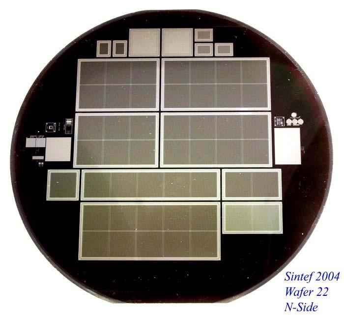
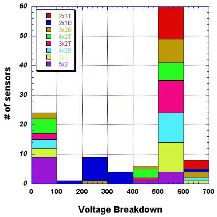
5 HV operations Guard Rings Finalized in 1999 with the engineering run PSI JHU PURDUE BTeV Two vendors Sintef CSEM (later Colibris later out of business) Vdep ~ V 10+1 Guard rings add ~1.2 mm on each edge of the sensor Holds >1000V before irradiation Holds >800V after Current (A) Current (A) 1.E-08 1.E-09 1.E-10 1.E-11 1.E-06 1.E-07 1.E-08 1.E-09 1.E-10 1.E-11 1.E-12 6 Guard Ring Diodes Diode 2 Diode 3 Diode 4 Diode Reverse Bias (V) 16 Guard Ring Diodes Reverse Bias (V) 11 Guard Ring Diodes Diode P11 Diode P32 Diode P31 Diode P11 1.E Current (A) 1.E-08 1.E-09 1.E-10 Reverse Bias Voltage (V) Diode 3 Diode 4 Diode 11 Diode 14 Diode 20 Nucl.Instrum.Meth.A461: ,2001 Leakage Current (A) S22 P47 Diode S22p29 1.E-03 S24p29 1.E-04 1.E-05 1.E-06 1.E-07 S4p47 φ = n eq /cm Reverse Bias (V) 5


6 HV operations p stops P stops edges are the points with high electric field Shapes and distances strongly affects the maximum HV reachable TDR TDR NOW NOW Nucl.Instrum.Meth.A501: ,2003 6


 PSI43")


7 F and FM design 2001: submission with Sintef with Only 2 design left for large sensors PSI30 Honeywell (irradiated and bumped at PSI) PSI43 DMILL (bumped at MCNC and IZM) PSI46 ¼ μm (bumped at IZM and VTT) Assembly experience CCE measurements Test beam F FM 7
.")
8 P stops geometry and CCE (Charge Collection Efficiency) 1064 nm laser (goes through more than 300 μm of Si) Beam size ~10 μm Scans in 2 μm steps Technique allows: One to one comparison on the CCE performance of the 2 design (F and FM). Dependence on Vbias Implanted n+ pixel (also metalized) ~98 μm square P stops ring 8 μm wide with 12 μm gaps Metal grid on the p side Contact between the Al and the n+ implanted pixel 8

9 F vs FM direct comparison F design at 320 V FM design at 320 V 9
 allows for more over depletion to be applied and so better CCE (lower inefficiencies) in the corner regions.")
10 CCE vs Vbias FM design at 250 V FM design at 350 V The decision to move to a higher resistivity ( V depletion on diodes versus the V of the 2001 submission) allows for more over depletion to be applied and so better CCE (lower inefficiencies) in the corner regions. 10


11 Can we squeeze it even more? FM FMM 11

12 FNAL Test beam strip pixel strip 120Gev Proton 12
13 FNAL Test beam beam : 120GeV Proton, 6-12 spills/min, few 1000 trgs/spill, 300events/spill, 4 strip planes (upstream) + pixel + 4 strip planes (downstream) Operation temperature : C vertical vertical beam pixel y z horizontal horizontal cm beam z strips pixel 20 o strips x 13
 1 plane = 2")


14 FNAL Test beam Beam telescope 8 strip planes( 4X + 4Y) 1 plane = 2 ROC s = 2 x 128 ch Strips pitch : 50um x1 2.3um y1 2.3um x2 y2 2.6um 2.6um x3 y3 2.8um 2.4um single cluster is used for tracking alignment variables : theta, offset track_residual < 3um x4 2.5um y4 2.2um 14

15 FNAL Test beam Months of data taking with the DMILL PSI43 Unstable performance 12/20/04 switched to ¼ μm PSI46v1 Reliable operation and robust efficiency measurements No charge information: a binary chip Pixel detector Sensor design : FM 4160 pixels/roc Chip : PSI46v1, 1x2 chip 1 chip has 52 columns and 80 rows 8.1 mm x 8.1 mm No charge information Pixel size : 150um(col) x 100um(row) 15
16 Data set Not tilted Tilt 20 degree run Bias Volt. Data Size run Bias Volt. Data Size 2635* * 2650* 2653* Runs with the * have been combined to get a high statistic sample 16
17 Cuts Number listed here for the 1M evts (4 runs combined) Cut Single track from the telescope Track quality Pointing to the pixel array BAD TBM trailer Find pixel hits Trk pixel residual Number of events ~ 1M System/Sensor efficiency 30% have multiple tracks 15% with single tracks have poor track resolution 18 % are pointing outside of the pixel array A small percentage have DAQ troubles 99.6 ± 0.3 % 99.3 ± 0.3 % 17
")

18 No tilt Efficiency: 99.3 ± 0.3 % 150um efficiency column 150um (Column) efficiency row 100um 100um (Row) Inefficiency is dominant at the corner of 4 pixels Consistent with the laser results 18
19 Rotation: 0 vs 20 Bias Voltage # of Events Good trk Good hits Efficiency % % % % % % 350 1M % % % % 19
20 Post irradiation: CERN CERN test beam data from fall 2004 Different ROC PSI30 (Honeywell from late 90s) Different pitch 125μm x 125 μm Analog charge available Threshold less Pre bump irradiation at CERN ( ) Bumped at PSI (indium) Single die metallurgy Many un bonded pixels Post irradiation efficiency measurements 20

21 Data set Illumination Sensor Bias Volt. Dose # of events F 300 Unirradiated FM FM No un irradiated FM design to be compared with the results from FNAL 21
22 Efficiency measurements 3000 e 97 % 22
23 Other results Signal to noise ratio of ~44 post irradiation (~45 for the p spray as a comparison) No evidences of micro discharges up to 600 V on irradiated device True also around un bonded pixels 4 Corners 4 Sides 23
24 Conclusions Sensors for the CMS FPIX project have been developed. The geometry is driven by the other components of the system High voltage operation are guaranteed according to the TDR specification The particle detection efficiency is > 99% before any irradiation and after 6x10 14 is still above 97 % The designed sensors are fully compatible with the goals of the project Daniela will present the results from the preproduction run 24
Thin Silicon R&D for LC applications
 Thin Silicon R&D for LC applications D. Bortoletto Purdue University Status report Hybrid Pixel Detectors for LC Next Linear Collider:Physic requirements Vertexing 10 µ mgev σ r φ,z(ip ) 5µ m 3 / 2 p sin
Prototype Performance and Design of the ATLAS Pixel Sensor
 Prototype Performance and Design of the ATLAS Pixel Sensor F. Hügging, for the ATLAS Pixel Collaboration Contents: - Introduction - Sensor Concept - Performance fi before and after irradiation - Conclusion
Development of Pixel Detectors for the Inner Tracker Upgrade of the ATLAS Experiment
 Development of Pixel Detectors for the Inner Tracker Upgrade of the ATLAS Experiment Natascha Savić L. Bergbreiter, J. Breuer, A. Macchiolo, R. Nisius, S. Terzo IMPRS, Munich # 29.5.215 Franz Dinkelacker
The CMS Pixel Detector Upgrade and R&D Developments for the High Luminosity LHC
 The CMS Pixel Detector Upgrade and R&D Developments for the High Luminosity LHC On behalf of the CMS Collaboration INFN Florence (Italy) 11th 15th September 2017 Las Caldas, Asturias (Spain) High Luminosity
Quality Assurance for the ATLAS Pixel Sensor
 Quality Assurance for the ATLAS Pixel Sensor 1st Workshop on Quality Assurance Issues in Silicon Detectors J. M. Klaiber-Lodewigs (Univ. Dortmund) for the ATLAS pixel collaboration Contents: - role of
Phase 1 upgrade of the CMS pixel detector
 Phase 1 upgrade of the CMS pixel detector, INFN & University of Perugia, On behalf of the CMS Collaboration. IPRD conference, Siena, Italy. Oct 05, 2016 1 Outline The performance of the present CMS pixel
Pixel sensors with different pitch layouts for ATLAS Phase-II upgrade
 Pixel sensors with different pitch layouts for ATLAS Phase-II upgrade Different pitch layouts are considered for the pixel detector being designed for the ATLAS upgraded tracking system which will be operating
Monolithic Pixel Sensors in SOI technology R&D activities at LBNL
 Monolithic Pixel Sensors in SOI technology R&D activities at LBNL Lawrence Berkeley National Laboratory M. Battaglia, L. Glesener (UC Berkeley & LBNL), D. Bisello, P. Giubilato (LBNL & INFN Padova), P.
CMS Tracker Upgrades. R&D Plans, Present Status and Perspectives. Benedikt Vormwald Hamburg University on behalf of the CMS collaboration
 R&D Plans, Present Status and Perspectives Benedikt Vormwald Hamburg University on behalf of the CMS collaboration EPS-HEP 2015 Vienna, 22.-29.07.2015 CMS Tracker Upgrade Program LHC HL-LHC ECM[TeV] 7-8
The INFN R&D: new pixel detector for the High Luminosity Upgrade of the LHC
 IFAE 17: XVI Incontri di fisica delle alte energie The INFN R&D: new pixel detector for the High Luminosity Upgrade of the LHC INFN Pixel R&D: main design features CMS results: thin-planar before & after
A new strips tracker for the upgraded ATLAS ITk detector
 A new strips tracker for the upgraded ATLAS ITk detector, on behalf of the ATLAS Collaboration : 11th International Conference on Position Sensitive Detectors 3-7 The Open University, Milton Keynes, UK.
The LHCb VELO Upgrade. Stefano de Capua on behalf of the LHCb VELO group
 The LHCb VELO Upgrade Stefano de Capua on behalf of the LHCb VELO group Overview [J. Instrum. 3 (2008) S08005] LHCb / Current VELO / VELO Upgrade Posters M. Artuso: The Silicon Micro-strip Upstream Tracker
Measurements With Irradiated 3D Silicon Strip Detectors
 Measurements With Irradiated 3D Silicon Strip Detectors Michael Köhler, Michael Breindl, Karls Jakobs, Ulrich Parzefall, Liv Wiik University of Freiburg Celeste Fleta, Manuel Lozano, Giulio Pellegrini
Strip Detectors. Principal: Silicon strip detector. Ingrid--MariaGregor,SemiconductorsasParticleDetectors. metallization (Al) p +--strips
 p +--strips") Strip Detectors First detector devices using the lithographic capabilities of microelectronics First Silicon detectors -- > strip detectors Can be found in all high energy physics experiments of the last
Strip Detectors First detector devices using the lithographic capabilities of microelectronics First Silicon detectors -- > strip detectors Can be found in all high energy physics experiments of the last
The High-Voltage Monolithic Active Pixel Sensor for the Mu3e Experiment
 The High-Voltage Monolithic Active Pixel Sensor for the Mu3e Experiment Shruti Shrestha On Behalf of the Mu3e Collaboration International Conference on Technology and Instrumentation in Particle Physics
Fluence dependence of charge collection of irradiated pixel sensors
 Physics Physics Research Publications Purdue University Year 2005 Fluence dependence of charge collection of irradiated pixel sensors T. Rohe, D. Bortoletto, V. Chlochia, L. M. Cremaldi, S. Cucciarelli,
 http://clicdp.cern.ch Hybrid Pixel Detectors with Active-Edge Sensors for the CLIC Vertex Detector Simon Spannagel on behalf of the CLICdp Collaboration Experimental Conditions at CLIC CLIC beam structure
Why p-type is better than n-type? or Electric field in heavily irradiated silicon detectors
 Why p-type is better than n-type? or Electric field in heavily irradiated silicon detectors G.Kramberger, V. Cindro, I. Mandić, M. Mikuž, M. Milovanović, M. Zavrtanik Jožef Stefan Institute Ljubljana,
Silicon Sensor Developments for the CMS Tracker Upgrade
 Silicon Sensor Developments for the CMS Tracker Upgrade on behalf of the CMS tracker collaboration University of Hamburg, Germany E-mail: Joachim.Erfle@desy.de CMS started a campaign to identify the future
Studies on MCM D interconnections
 Studies on MCM D interconnections Speaker: Peter Gerlach Department of Physics Bergische Universität Wuppertal D-42097 Wuppertal, GERMANY Authors: K.H.Becks, T.Flick, P.Gerlach, C.Grah, P.Mättig Department
The Compact Muon Solenoid Experiment. Conference Report. Mailing address: CMS CERN, CH-1211 GENEVA 23, Switzerland
 Available on CMS information server CMS CR -2015/213 The Compact Muon Solenoid Experiment Conference Report Mailing address: CMS CERN, CH-1211 GENEVA 23, Switzerland 05 October 2015 (v2, 12 October 2015)
PoS(VERTEX2015)008. The LHCb VELO upgrade. Sophie Elizabeth Richards. University of Bristol
008. The LHCb VELO upgrade. Sophie Elizabeth Richards. University of Bristol") University of Bristol E-mail: sophie.richards@bristol.ac.uk The upgrade of the LHCb experiment is planned for beginning of 2019 unitl the end of 2020. It will transform the experiment to a trigger-less
University of Bristol E-mail: sophie.richards@bristol.ac.uk The upgrade of the LHCb experiment is planned for beginning of 2019 unitl the end of 2020. It will transform the experiment to a trigger-less
Towards a 10 μs, thin high resolution pixelated CMOS sensor system for future vertex detectors
 Towards a 10 μs, thin high resolution pixelated CMOS sensor system for future vertex detectors Rita De Masi IPHC-Strasbourg On behalf of the IPHC-IRFU collaboration Physics motivations. Principle of operation
Performance of a Single-Crystal Diamond-Pixel Telescope
 University of Tennessee, Knoxville From the SelectedWorks of stefan spanier 29 Performance of a Single-Crystal Diamond-Pixel Telescope R. Hall-Wilton V. Ryjov M. Pernicka V. Halyo B. Harrop, et al. Available
CMS Tracker Upgrade for HL-LHC Sensors R&D. Hadi Behnamian, IPM On behalf of CMS Tracker Collaboration
 CMS Tracker Upgrade for HL-LHC Sensors R&D Hadi Behnamian, IPM On behalf of CMS Tracker Collaboration Outline HL-LHC Tracker Upgrade: Motivations and requirements Silicon strip R&D: * Materials with Multi-Geometric
ITk silicon strips detector test beam at DESY
 ITk silicon strips detector test beam at DESY Lucrezia Stella Bruni Nikhef Nikhef ATLAS outing 29/05/2015 L. S. Bruni - Nikhef 1 / 11 Qualification task I Participation at the ITk silicon strip test beams
Preparing for the Future: Upgrades of the CMS Pixel Detector
 : KSETA Plenary Workshop, Durbach, KIT Die Forschungsuniversität in der Helmholtz-Gemeinschaft www.kit.edu Large Hadron Collider at CERN Since 2015: proton proton collisions @ 13 TeV Four experiments:
The LHCb Vertex Locator : Marina Artuso, Syracuse University for the VELO Group
 The LHCb Vertex Locator : status and future perspectives Marina Artuso, Syracuse University for the VELO Group The LHCb Detector Mission: Expore interference of virtual new physics particle in the decays
Test Beam Measurements for the Upgrade of the CMS Phase I Pixel Detector
 Test Beam Measurements for the Upgrade of the CMS Phase I Pixel Detector Simon Spannagel on behalf of the CMS Collaboration 4th Beam Telescopes and Test Beams Workshop February 4, 2016, Paris/Orsay, France
The BaBar Silicon Vertex Tracker (SVT) Claudio Campagnari University of California Santa Barbara
 Claudio Campagnari University of California Santa Barbara") The BaBar Silicon Vertex Tracker (SVT) Claudio Campagnari University of California Santa Barbara Outline Requirements Detector Description Performance Radiation SVT Design Requirements and Constraints
The BaBar Silicon Vertex Tracker (SVT) Claudio Campagnari University of California Santa Barbara Outline Requirements Detector Description Performance Radiation SVT Design Requirements and Constraints
Production of HPDs for the LHCb RICH Detectors
 Production of HPDs for the LHCb RICH Detectors LHCb RICH Detectors Hybrid Photon Detector Production Photo Detector Test Facilities Test Results Conclusions IEEE Nuclear Science Symposium Wyndham, 24 th
Resolution studies on silicon strip sensors with fine pitch
 Resolution studies on silicon strip sensors with fine pitch Stephan Hänsel This work is performed within the SiLC R&D collaboration. LCWS 2008 Purpose of the Study Evaluate the best strip geometry of silicon
Pixel hybrid photon detectors
 Pixel hybrid photon detectors for the LHCb-RICH system Ken Wyllie On behalf of the LHCb-RICH group CERN, Geneva, Switzerland 1 Outline of the talk Introduction The LHCb detector The RICH 2 counter Overall
Development of CMOS pixel sensors for tracking and vertexing in high energy physics experiments
 PICSEL group Development of CMOS pixel sensors for tracking and vertexing in high energy physics experiments Serhiy Senyukov (IPHC-CNRS Strasbourg) on behalf of the PICSEL group 7th October 2013 IPRD13,
PoS(Vertex 2016)071. The LHCb VELO for Phase 1 Upgrade. Cameron Dean, on behalf of the LHCb Collaboration
071. The LHCb VELO for Phase 1 Upgrade. Cameron Dean, on behalf of the LHCb Collaboration") The LHCb VELO for Phase 1 Upgrade, on behalf of the LHCb Collaboration University of Glasgow E-mail: cameron.dean@cern.ch Large Hadron Collider beauty (LHCb) is a dedicated experiment for studying b and
The LHCb VELO for Phase 1 Upgrade, on behalf of the LHCb Collaboration University of Glasgow E-mail: cameron.dean@cern.ch Large Hadron Collider beauty (LHCb) is a dedicated experiment for studying b and
Attilio Andreazza INFN and Università di Milano for the ATLAS Collaboration The ATLAS Pixel Detector Efficiency Resolution Detector properties
 10 th International Conference on Large Scale Applications and Radiation Hardness of Semiconductor Detectors Offline calibration and performance of the ATLAS Pixel Detector Attilio Andreazza INFN and Università
Julia Thom-Levy, Cornell University, for the CMS Collaboration. ECFA High Luminosity LHC Experiments Workshop-2016 October 3-6, 2016
 J.Thom-Levy October 5th, 2016 ECFA High Lumi LHC Experiments Pixel Detector R&D 1 Pixel Tracker R&D Cornell University Floyd R. Newman Laboratory for Elementary-Particle Physics Julia Thom-Levy, Cornell
The HGTD: A SOI Power Diode for Timing Detection Applications
 The HGTD: A SOI Power Diode for Timing Detection Applications Work done in the framework of RD50 Collaboration (CERN) M. Carulla, D. Flores, S. Hidalgo, D. Quirion, G. Pellegrini IMB-CNM (CSIC), Spain
2 nd ACES workshop, CERN. Hans-Christian Kästli, PSI
 CMS Pixel Upgrade 2 nd ACES workshop, CERN Hans-Christian Kästli, PSI 3.3.2009 Scope Phase I (~2013): CMS pixel detector designed for fast insertion/removal Can replace system during normal shutdown Planned
BaBar SVT: Radiation Damage and Other Operational Issues
 BaBar SVT: Radiation Damage and Other Operational Issues SLAC 1 Outline 2 Intro to BaBar and SVT Radiation Environment Damage to Si Detectors Damage to Front End Electronics Performance Degradation Other
10.01: Development of Radiation Hard Pixel Detectors for the CMS Tracker Upgrade for the SLHC
 CMS Upgrade MB Response to SLHC Document: 10.01: Development of Radiation Hard Pixel Detectors for the CMS Tracker Upgrade for the SLHC (Contact Person: Simon Kwan, Fermilab) It is our intent to recommend
Design and characterization of the monolithic matrices of the H35DEMO chip
 Design and characterization of the monolithic matrices of the H35DEMO chip Raimon Casanova 1,a Institut de Física d Altes Energies (IFAE), The Barcelona Institute of Science and Technology (BIST) Edifici
The CMS Silicon Pixel Detector for HL-LHC
 * Institute for Experimental Physics Hamburg University Luruper Chaussee 149 22761 Hamburg, Germany E-mail: georg.steinbrueck@desy.de for the CMS collaboration The LHC is planning an upgrade program which
Anders Ryd Cornell University April 24, Outline: CMS Pixel and Strip tracker Implementation Current status and plans
 The CMS Pixel Detector Cornell University April 24, 2007 Outline: CMS Pixel and Strip tracker Implementation Current status and plans Page: 1 LHC and CMS Physics Goals The LHC will collide protons on protons
Studies of silicon strip sensors for the ATLAS ITK project. Miguel Arratia Cavendish Laboratory, University of Cambridge
 Studies of silicon strip sensors for the ATLAS ITK project Miguel Arratia Cavendish Laboratory, University of Cambridge 1 ITK project and radiation damage Unprecedented large fluences expected for the
Radiation hardness and precision timing study of Silicon Detectors for the CMS High Granularity Calorimeter (HGC)
") Radiation hardness and precision timing study of Silicon Detectors for the CMS High Granularity Calorimeter (HGC) Esteban Currás1,2, Marcos Fernández2, Christian Gallrapp1, Marcello Mannelli1, Michael
Radiation hardness and precision timing study of Silicon Detectors for the CMS High Granularity Calorimeter (HGC) Esteban Currás1,2, Marcos Fernández2, Christian Gallrapp1, Marcello Mannelli1, Michael
Review of Silicon Inner Tracker
 Review of Silicon Inner Tracker H.J.Kim (KyungPook National U.) Talk Outline Configuration optimization of BIT and FIT Silicon Sensor R&D Electronics R&D Summary and Plan Detail study will be presented
Summary of CMS Pixel Group Preparatory Workshop on Upgrades
 Available on CMS information server CMS NOTE 2007/000 December 14, 2006 Summary of CMS Pixel Group Preparatory Workshop on Upgrades D. Bortoletto Purdue University, West Lafayette, IN, USA K. Burkett,
Textmasterformat bearbeiten
 Status of Sensors: Measurements on the AGIPD Sensors (from 1st batch to 2nd batch) Jiaguo Zhang1, Robert Klanner2, Ioannis Kopsalis2, and Joern Schwandt2 1 Photon Science Detector Group (FSDS), DESY 2
Simulation of High Resistivity (CMOS) Pixels
 Pixels") Simulation of High Resistivity (CMOS) Pixels Stefan Lauxtermann, Kadri Vural Sensor Creations Inc. AIDA-2020 CMOS Simulation Workshop May 13 th 2016 OUTLINE 1. Definition of High Resistivity Pixel Also
Simulation of High Resistivity (CMOS) Pixels Stefan Lauxtermann, Kadri Vural Sensor Creations Inc. AIDA-2020 CMOS Simulation Workshop May 13 th 2016 OUTLINE 1. Definition of High Resistivity Pixel Also
Liejian Chen (IHEP) On behalf of IHEP ATLAS Group
 On behalf of IHEP ATLAS Group") Liejian Chen (IHEP) On behalf of IHEP ATLAS Group Many thanks for ATLAS CMOS Strip Calibration Yubo Han 1, Hongbo Zhu 1, Giulio Villani 2, Iain Sedgwick 2, Jens Dopke 2, Zhige Zhang 2, Steve MacMahon 2,
Liejian Chen (IHEP) On behalf of IHEP ATLAS Group Many thanks for ATLAS CMOS Strip Calibration Yubo Han 1, Hongbo Zhu 1, Giulio Villani 2, Iain Sedgwick 2, Jens Dopke 2, Zhige Zhang 2, Steve MacMahon 2,
The Architecture of the BTeV Pixel Readout Chip
 The Architecture of the BTeV Pixel Readout Chip D.C. Christian, dcc@fnal.gov Fermilab, POBox 500 Batavia, IL 60510, USA 1 Introduction The most striking feature of BTeV, a dedicated b physics experiment
VErtex LOcator (VELO)
") Commissioning the LHCb VErtex LOcator (VELO) Mark Tobin University of Liverpool On behalf of the LHCb VELO group 1 Overview Introduction LHCb experiment. The Vertex Locator (VELO). Description of System.
Commissioning the LHCb VErtex LOcator (VELO) Mark Tobin University of Liverpool On behalf of the LHCb VELO group 1 Overview Introduction LHCb experiment. The Vertex Locator (VELO). Description of System.
ATLAS strip detector upgrade for the HL-LHC
 ATL-INDET-PROC-2015-010 26 August 2015, On behalf of the ATLAS collaboration Santa Cruz Institute for Particle Physics, University of California, Santa Cruz E-mail: zhijun.liang@cern.ch Beginning in 2024,
Status of ATLAS & CMS Experiments
 Status of ATLAS & CMS Experiments Atlas S.C. Magnet system Large Air-Core Toroids for µ Tracking 2Tesla Solenoid for inner Tracking (7*2.5m) ECAL & HCAL outside Solenoid Solenoid integrated in ECAL Barrel
CMOS pixel sensor development for the ATLAS experiment at the High Luminosity-LHC
 Prepared for submission to JINST The 11 th International Conference on Position Sensitive Detectors 3-8 September 2017 The Open University, Milton Keynes, UK. CMOS pixel sensor development for the ATLAS
Monolithic Pixel Detector in a 0.15µm SOI Technology
 Monolithic Pixel Detector in a 0.15µm SOI Technology 2006 IEEE Nuclear Science Symposium, San Diego, California, Nov. 1, 2006 Yasuo Arai (KEK) KEK Detector Technology Project : [SOIPIX Group] Y. Arai Y.
Sensor Concepts for Pixel Detectors in HEP
 Introduction "p in n" Sensors design, te, limits in radiation hardness "n in n" Sensors for LHC Experiments radiation hardness requirements n side isolation and design Other Experiments "Super LHC" TESLA
National Accelerator Laboratory
 Fermi National Accelerator Laboratory FERMILAB-Conf-97/343-E D0 Preliminary Results from the D-Zero Silicon Vertex Beam Tests Maria Teresa P. Roco For the D0 Collaboration Fermi National Accelerator Laboratory
A High-Granularity Timing Detector for the Phase-II upgrade of the ATLAS Detector system
 A High-Granularity Timing Detector for the Phase-II upgrade of the ATLAS Detector system C.Agapopoulou on behalf of the ATLAS Lar -HGTD group 2017 IEEE Nuclear Science Symposium and Medical Imaging Conference
BTeV Pixel Detector and Silicon Forward Tracker
 BTeV Pixel Detector and Silicon Forward Tracker Simon Kwan Fermilab VERTEX2002, Kailua-Kona, November 4, 2002 BTeV Overview Technical Design R&D Status Conclusion OUTLINE What is BTeV? At the Tevatron
Study of the radiation-hardness of VCSEL and PIN
 Study of the radiation-hardness of VCSEL and PIN 1, W. Fernando, H.P. Kagan, R.D. Kass, H. Merritt, J.R. Moore, A. Nagarkara, D.S. Smith, M. Strang Department of Physics, The Ohio State University 191
Single-sided p n and double-sided silicon strip detectors exposed to fluences up to 2 10 /cm 24 GeV protons
 Nuclear Instruments and Methods in Physics Research A 409 (1998) 184 193 Single-sided p n and double-sided silicon strip detectors exposed to fluences up to 2 10 /cm 24 GeV protons L. Andricek, T. Gebhart,
Light High Precision CMOS Pixel Devices Providing 0(µs) Timestamping for Future Vertex Detectors
 Timestamping for Future Vertex Detectors") Light High Precision CMOS Pixel Devices Providing 0(µs) Timestamping for Future Vertex Detectors M. Winter, on behalf of PICSEL team of IPHC-Strasbourg IEEE/NSS-MIC - Anaheim(CA) Novembre 2012 Contents
Light High Precision CMOS Pixel Devices Providing 0(µs) Timestamping for Future Vertex Detectors M. Winter, on behalf of PICSEL team of IPHC-Strasbourg IEEE/NSS-MIC - Anaheim(CA) Novembre 2012 Contents
Results of FE65-P2 Pixel Readout Test Chip for High Luminosity LHC Upgrades
 for High Luminosity LHC Upgrades R. Carney, K. Dunne, *, D. Gnani, T. Heim, V. Wallangen Lawrence Berkeley National Lab., Berkeley, USA e-mail: mgarcia-sciveres@lbl.gov A. Mekkaoui Fermilab, Batavia, USA
The LHCb Vertex Locator (VELO) Pixel Detector Upgrade
 Pixel Detector Upgrade") Home Search Collections Journals About Contact us My IOPscience The LHCb Vertex Locator (VELO) Pixel Detector Upgrade This content has been downloaded from IOPscience. Please scroll down to see the full
Home Search Collections Journals About Contact us My IOPscience The LHCb Vertex Locator (VELO) Pixel Detector Upgrade This content has been downloaded from IOPscience. Please scroll down to see the full
Gamma-ray Large Area Space Telescope (GLAST) Large Area Telescope (LAT) Silicon Detector Specification
 Large Area Telescope (LAT) Silicon Detector Specification") GLAST LAT PROCUREMENT SPECIFICATION Document # Document Title GLAST LAT Silicon Detector Specification Date Effective Page 1 of 21 GE-00011-A 1rst Draft 8/20/00 Author(s) Supersedes H. Sadrozinski T. Ohsugi
GLAST LAT PROCUREMENT SPECIFICATION Document # Document Title GLAST LAT Silicon Detector Specification Date Effective Page 1 of 21 GE-00011-A 1rst Draft 8/20/00 Author(s) Supersedes H. Sadrozinski T. Ohsugi
High-Speed/Radiation-Hard Optical Links
 High-Speed/Radiation-Hard Optical Links K.K. Gan, H. Kagan, R. Kass, J. Moore, D.S. Smith The Ohio State University P. Buchholz, S. Heidbrink, M. Vogt, M. Ziolkowski Universität Siegen September 8, 2016
arxiv: v2 [physics.ins-det] 15 Feb 2013
![arxiv: v2 [physics.ins-det] 15 Feb 2013](/thumbs/91/105524489.jpg "arxiv: v2 [physics.ins-det] 15 Feb 2013") Novel Silicon n-on-p Edgeless Planar Pixel Sensors for the ATLAS upgrade arxiv:1212.3580v2 [physics.ins-det] 15 Feb 2013 1 2 3 4 5 6 7 8 9 10 11 12 13 14 15 16 17 18 M. Bomben a,, A. Bagolini b, M. Boscardin
Novel Silicon n-on-p Edgeless Planar Pixel Sensors for the ATLAS upgrade arxiv:1212.3580v2 [physics.ins-det] 15 Feb 2013 1 2 3 4 5 6 7 8 9 10 11 12 13 14 15 16 17 18 M. Bomben a,, A. Bagolini b, M. Boscardin
ATLAS Upgrade SSD. ATLAS Upgrade SSD. Specifications of Electrical Measurements on SSD. Specifications of Electrical Measurements on SSD
 ATLAS Upgrade SSD Specifications of Electrical Measurements on SSD ATLAS Project Document No: Institute Document No. Created: 17/11/2006 Page: 1 of 7 DRAFT 2.0 Modified: Rev. No.: 2 ATLAS Upgrade SSD Specifications
PoS(VERTEX 2009)037. The LHCb VELO Upgrade. Jianchun Wang 1
037. The LHCb VELO Upgrade. Jianchun Wang 1") 1 Syracuse University Department of Physics, Syracuse University, Syracuse NY 13244, U.S.A E-mail: jwang@physics.syr.edu The LHCb experiment is dedicated to study CP violation and other rare phenomena
1 Syracuse University Department of Physics, Syracuse University, Syracuse NY 13244, U.S.A E-mail: jwang@physics.syr.edu The LHCb experiment is dedicated to study CP violation and other rare phenomena
The CMS Pixel Detector Phase-1 Upgrade
 Paul Scherrer Institut, Switzerland E-mail: wolfram.erdmann@psi.ch The CMS experiment is going to upgrade its pixel detector during Run 2 of the Large Hadron Collider. The new detector will provide an
irst: process development, characterization and first irradiation studies
 3D D detectors at ITC-irst irst: process development, characterization and first irradiation studies S. Ronchin a, M. Boscardin a, L. Bosisio b, V. Cindro c, G.-F. Dalla Betta d, C. Piemonte a, A. Pozza
ATLAS ITk and new pixel sensors technologies
 IL NUOVO CIMENTO 39 C (2016) 258 DOI 10.1393/ncc/i2016-16258-1 Colloquia: IFAE 2015 ATLAS ITk and new pixel sensors technologies A. Gaudiello INFN, Sezione di Genova and Dipartimento di Fisica, Università
Study of irradiated 3D detectors. University of Glasgow, Scotland. University of Glasgow, Scotland
 Department of Physics & Astronomy Experimental Particle Physics Group Kelvin Building, University of Glasgow Glasgow, G12 8QQ, Scotland Telephone: ++44 (0)141 339 8855 Fax: +44 (0)141 330 5881 GLAS-PPE/2002-20
Muon detection in security applications and monolithic active pixel sensors
 Muon detection in security applications and monolithic active pixel sensors Tracking in particle physics Gaseous detectors Silicon strips Silicon pixels Monolithic active pixel sensors Cosmic Muon tomography
A novel solution for various monitoring applications at CERN
 A novel solution for various monitoring applications at CERN F. Lackner, P. H. Osanna 1, W. Riegler, H. Kopetz CERN, European Organisation for Nuclear Research, CH-1211 Geneva-23, Switzerland 1 Department
The ATLAS tracker Pixel detector for HL-LHC
 on behalf of the ATLAS Collaboration INFN Genova E-mail: Claudia.Gemme@ge.infn.it The high luminosity upgrade of the LHC (HL-LHC) in 2026 will provide new challenges to the ATLAS tracker. The current Inner
Status of ITC-irst activities in RD50
 Status of ITC-irst activities in RD50 M. Boscardin ITC-irst, Microsystem Division Trento, Italy Outline Materials/Pad Detctors Pre-irradiated silicon INFN Padova and Institute for Nuclear Research of NASU,
 Frank.Hartmann@CERN.CH 03.02.2012 Content & Disclaimer Different Strategies FLUKA Leakage currents Depletion Voltage Each experiment is following the same goal but with slightly different strategies An
UNIVERSITY of CALIFORNIA SANTA CRUZ
 UNIVERSITY of CALIFORNIA SANTA CRUZ CHARACTERIZATION OF THE IRST PROTOTYPE P-TYPE SILICON STRIP SENSOR A thesis submitted in partial satisfaction of the requirements for the degree of BACHELOR OF SCIENCE
Silicon Sensor and Detector Developments for the CMS Tracker Upgrade
 Silicon Sensor and Detector Developments for the CMS Tracker Upgrade Università degli Studi di Firenze and INFN Sezione di Firenze E-mail: candi@fi.infn.it CMS has started a campaign to identify the future
`First ep events in the Zeus micro vertex detector in 2002`
 Amsterdam 18 dec 2002 `First ep events in the Zeus micro vertex detector in 2002` Erik Maddox, Zeus group 1 History (1): HERA I (1992-2000) Lumi: 117 pb -1 e +, 17 pb -1 e - Upgrade (2001) HERA II (2001-2006)
Radiation-hard active CMOS pixel sensors for HL- LHC detector upgrades
 Journal of Instrumentation OPEN ACCESS Radiation-hard active CMOS pixel sensors for HL- LHC detector upgrades To cite this article: Malte Backhaus Recent citations - Module and electronics developments
Upgrade of the CMS Tracker for the High Luminosity LHC
 Upgrade of the CMS Tracker for the High Luminosity LHC * CERN E-mail: georg.auzinger@cern.ch The LHC machine is planning an upgrade program which will smoothly bring the luminosity to about 5 10 34 cm
OPTICAL LINK OF THE ATLAS PIXEL DETECTOR
 OPTICAL LINK OF THE ATLAS PIXEL DETECTOR K.K. Gan, W. Fernando, P.D. Jackson, M. Johnson, H. Kagan, A. Rahimi, R. Kass, S. Smith Department of Physics, The Ohio State University, Columbus, OH 43210, USA
CMOS Detectors Ingeniously Simple!
 CMOS Detectors Ingeniously Simple! A.Schöning University Heidelberg B-Workshop Neckarzimmern 18.-20.2.2015 1 Detector System on Chip? 2 ATLAS Pixel Module 3 ATLAS Pixel Module MCC sensor FE-Chip FE-Chip
PoS(EPS-HEP 2009)150. Silicon Detectors for the slhc - an Overview of Recent RD50 Results. Giulio Pellegrini 1. On behalf of CERN RD50 collaboration
150. Silicon Detectors for the slhc - an Overview of Recent RD50 Results. Giulio Pellegrini 1. On behalf of CERN RD50 collaboration") Silicon Detectors for the slhc - an Overview of Recent RD50 Results 1 Centro Nacional de Microelectronica CNM- IMB-CSIC, Barcelona Spain E-mail: giulio.pellegrini@imb-cnm.csic.es On behalf of CERN RD50
Silicon Detectors for the slhc - an Overview of Recent RD50 Results 1 Centro Nacional de Microelectronica CNM- IMB-CSIC, Barcelona Spain E-mail: giulio.pellegrini@imb-cnm.csic.es On behalf of CERN RD50
Chapter 4 Vertex. Qun Ouyang. Nov.10 th, 2017Beijing. CEPC detector CDR mini-review
 Chapter 4 Vertex Qun Ouyang Nov.10 th, 2017Beijing Nov.10 h, 2017 CEPC detector CDR mini-review CEPC detector CDR mini-review Contents: 4 Vertex Detector 4.1 Performance Requirements and Detector Challenges
PoS(Vertex 2016)028. Small pitch 3D devices. Gian-Franco Dalla Betta 1, Roberto Mendicino, DMS Sultan
028. Small pitch 3D devices. Gian-Franco Dalla Betta 1, Roberto Mendicino, DMS Sultan") 1, Roberto Mendicino, DMS Sultan University of Trento and TIFPA INFN Via Sommarive, 9 38123 Trento, Italy E-mail: gianfranco.dallabetta@unitn.it Maurizio Boscardin, Gabriele Giacomini 2, Sabina Ronchin,
1, Roberto Mendicino, DMS Sultan University of Trento and TIFPA INFN Via Sommarive, 9 38123 Trento, Italy E-mail: gianfranco.dallabetta@unitn.it Maurizio Boscardin, Gabriele Giacomini 2, Sabina Ronchin,
Module Integration Sensor Requirements
 Module Integration Sensor Requirements Phil Allport Module Integration Working Group Sensor Geometry and Bond Pads Module Programme Issues Numbers of Sensors Required Nobu s Sensor Size Summary n.b. 98.99
Development of Double-sided Silcon microstrip Detector. D.H. Kah*, H. Park, H.J. Kim (BAERI JikLee (SNU) E. Won (Korea U)
 E. Won (Korea U)") Development of Double-sided Silcon microstrip Detector D.H. Kah*, H. Park, H.J. Kim (BAERI JikLee (SNU) E. Won (Korea U), KNU) 2005 APPI dhkah@belle.knu.ac.kr 1 1. Motivation 2. Introduction Contents 1.
Development of Double-sided Silcon microstrip Detector D.H. Kah*, H. Park, H.J. Kim (BAERI JikLee (SNU) E. Won (Korea U), KNU) 2005 APPI dhkah@belle.knu.ac.kr 1 1. Motivation 2. Introduction Contents 1.
Radiation Test Report Paul Scherer Institute Proton Irradiation Facility
 the Large Hadron Collider project CERN CH-2 Geneva 23 Switzerland CERN Div./Group RadWG EDMS Document No. xxxxx Radiation Test Report Paul Scherer Institute Proton Irradiation Facility Responsibility Tested
AIDA-2020 Advanced European Infrastructures for Detectors at Accelerators. Deliverable Report. CERN pixel beam telescope for the PS
 AIDA-2020-D15.1 AIDA-2020 Advanced European Infrastructures for Detectors at Accelerators Deliverable Report CERN pixel beam telescope for the PS Dreyling-Eschweiler, J (DESY) et al 25 March 2017 The AIDA-2020
The LHCb Silicon Tracker
 Journal of Instrumentation OPEN ACCESS The LHCb Silicon Tracker To cite this article: C Elsasser 214 JINST 9 C9 View the article online for updates and enhancements. Related content - Heavy-flavour production
AIDA Advanced European Infrastructures for Detectors at Accelerators. Journal Publication
 AIDA-PUB-13- AIDA Advanced European Infrastructures for Detectors at Accelerators Journal Publication Thin n-in-p pixel sensors and the SLID-ICV vertical integration technology for the ATLAS upgrade at
Development of silicon detectors for Beam Loss Monitoring at HL-LHC
 Development of silicon detectors for Beam Loss Monitoring at HL-LHC E. Verbitskaya, V. Eremin, A. Zabrodskii, A. Bogdanov, A. Shepelev Ioffe Institute, St. Petersburg, Russian Federation B. Dehning, M.
Towards a 10μs, thin high resolution pixelated CMOS sensor for future vertex detectors
 Towards a 10μs, thin high resolution pixelated CMOS sensor for future vertex detectors Yorgos Voutsinas IPHC Strasbourg on behalf of IPHC IRFU collaboration CMOS sensors principles Physics motivations
Position dependence of charge collection in prototype sensors for the CMS pixel detector
 Physics Physics Research Publications Purdue University Year 2004 Position dependence of charge collection in prototype sensors for the CMS pixel detector T. Rohe, D. Bortoletto, V. Chiochia, L. M. Cremaldi,
Simulation of new P-type strip detectors with trench to enhance the charge multiplication effect in the n- type electrodes
 Simulation of new P-Type strip detectors RESMDD 10, Florence 12-15.October.2010 1/15 Simulation of new P-type strip detectors with trench to enhance the charge multiplication effect in the n- type electrodes