Ultra-Wide-Band (UWB) Band-Pass-Filter Using Integrated Passive Device (IPD) Technology for Wireless Applications. STATS ChipPAC D&C YongTaek Lee
|
|
|
- Jerome Ralf Boyd
- 6 years ago
- Views:
Transcription
1 Ultra-Wide-Band (UWB) Band-Pass-Filter Using Integrated Passive Device (IPD) Technology for Wireless Applications June 17, 2009 STATS ChipPAC D&C YongTaek Lee Rev01
2 Agenda Introduction Design and characterization for flip-chip IPD Design and characterization ti for Wire bonding IPD The simple triple wire-bond and philips/tu Delgt tripe wire-bond inductance model Conclusions 2
3 Introduction Most common applications of Integrated passives devices (IPDs) are in the front-end of wireless systems, between the antenna and transceiver. Integrated passives devices (IPDs) based on semiconductor processes offer the advantage of excellent parameter control, and allow simplified and compact module design. IPD processes can be used to make high density capacitors, high Q inductors and large value resistors. The Ultra Wide Band (UWB) band-pass-filter developed in this paper has the smallest size while achieving i equivalent electrical l performance. In this paper, an UWB Band-pass-filter is made using lumped integrated passive devise technology on a silicon substrate for wireless applications. 3

 WLAN WLAN Wireline PAN 2G 2G 4G ZigBee Bludtooth 802.15.3 ADSL VDSL USB1.1 USB2.")
4 The technology of UWB UWB offers great potentials for home networking, wireless sensors, and location aware system. UWB Characteristics and signal. Low power BW = (f H -f L )/f c = 2(f H -f L )/(f H + f L ) High data rate Narrowband BW < 1% Wideband 1% < BW < 20% Ultra-Wide-Band BW > 20% Cellular (Mobile) WLAN WLAN Wireline PAN 2G 2G 4G ZigBee Bludtooth ADSL VDSL USB1.1 USB2.0 Trans smission Power Carrier based system (30KHz) Wireless LAN (5MHz) UWB(a few GHz) Data Rate (Mbps) Frequency 4


, Resistors: < 100K")

 structure (")
5 Integrated Passive Device Process Description In the STATS ChipPAC s silicon process, a specially treated silicon substrate is used to grow dielectric layer and metal layer. Capacitors: < 100pF, inductors: 20nH (Q 25-45), Resistors: < 100K Ohm. Component surface Component surface WIRE-BOND FLIP-CHIP Figure1: Thin film Integrated Passive Device (IPD) structure ( not in scale). Resistor Inductor Capacitor 5


")

6 RF Product Design Examples GSM LPF, Balun. DCS LPF, Balun. 11b/g BPF, Balun. 11a BPF, Balun. WiMax BPF, Balun. Diplexers: GSM/DCS, 11b/a, WiMax. Compact designs: Balanced filter, Balanced diplexers. RF Modules (CSMP) and RF SiP. IPD on wafer being probed IPD on substrate 6
7 IPD RF Applications (side by side with a die) IPD product databook available from the website. IMS2008, Atlanta 7


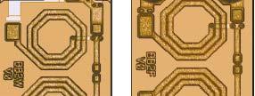
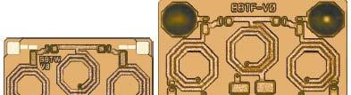
8 UWB Band-Pass-Filter for Flip-Chip IPD Figure 2 shows a circuit topology for the band-pass filter. Flip-chip IPD layout of the UWB band-pass-filter for EM simulation. Two bumps are for UWB band-pass-filter input and output. Four bumps are just for electrical ground. The UWB band-pass-filter of flip-chip die has a size of 1.4mm x 1.2mm x 0.40mm (including bump height). PORT03 C05 C08 PORT06 C04 C01 L01 C02 C07 PORT02 PORT05 L02 L03 C03 C06 PORT01 PORT04 Figure 2: Circuit topology for UWB bandpass-filter (BPF). Figure 3: Flip-chip IPD layout of the UWB band-pass-filter for EM simulation. 8

 Create circuit model for IPD Step: 2) Generate")
 Optimize as required to meet")
9 UWB Band-Pass-Filter for Flip-Chip IPD To meet electrical performance and size target a general design methodology (Figure 4) was followed. Step: 1) Create circuit model for IPD Step: 2) Generate physical layout to fit available space, and perform EM simulation Step: 3) Optimize as required to meet specifications. Figure 4: Design methodology of integrated passives. 9
10 UWB Band-Pass-Filter for Flip-Chip IPD The simulated characteristics of the UWB band-pass-filter are shown in Figure 5. The insertion loss from 7GHz to 9GHz is 1.8dB and the return loss is greater than 15dB in EM-simulation. Passband re eturn loss (S 11 db B) Passband in nsertion loss(s 1 db) Passband retrun loss S 11 Passband insertion loss S Frequency (GHz) Figure 5: S 11 and S 21 parameters for the UWB band-pass-filter in simulation. 10


11 Fabrication Passive integration on silicon substrate. Low insertion loss in pass band. Eutectic Sn/Pb or lead-free solder bump. Low profile, 0.40mm height. Directly flipped on PCB. Operating temperature: -40 to +85 C. Storage temperature: -40 to +85 C. Figure 6: UWB band-pass-filter flip-chip die. 11


12 Wafer Level Test Membrane probes for non-destructive wafer-level test. PCM for line width, leakage current, capacitance, inductor Q, etc. Ensure yield before wafers/dies shipped out. RF Wafer Membrane Probe 12
13 Characterization on Laminate Board S-Parameters were measured with wire bonding IPD die through probing on the G-S-G patterns on the test board. Verify the response in package. Temperature controller used for IPD temp characterization. IPD Flipped Probe Station G-S-G patterns on the test board Temperature Controller 13
14 UWB Band-Pass-Filter Results for Flip-Chip IPD Typical characteristics of the manufactured UWB band-pass-filter are shown in Figure 7. The insertion loss is 1.7dB (minimum) and return loss is 15dB. The manufactured UWB band-pass-filter has low pass-band insertion loss and small size. Insertio on Loss (db B) Insertion Loss Return Loss (db B) Return Loss Frequency (GHZ) Frequency (GHz) Figure 7: Typical characteristics of the manufactured UWB band-pass-filter. 14
15 UWB Band-Pass-Filter Results for Flip-Chip IPD Typical characteristics for the filp-chip UWB band-pass filter. In high frequency applications, our simulation scheme is very suitable for designing IPD products. Table 1: Typical characteristics for the flip-chip UWB band-pass filter. Specification Units Min Typ Max Design Measure ment Passband frequency MHz Passband insertion loss db Passband return loss db Attenuation, MHz db Attenuation, MHz db Attenuation, MHz db Attenuation, MHz db Attenuation, MHz db


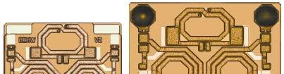
16 UWB Band-Pass-Filter for Wire Bonding IPD The circuit design and fabrication of the wire-bond UWB band-passfilter IPD are similar to those described above for the flip-chip device. The device can be mounted directly on a PCB or laminate substrate using conventional wire-bonding techniques. The UWB band-pass-filter of wire-bonding die has a size of 1.2mm x 1.0mm x 0.25mm. Figure 8: Wire bonding IPD layout of the UWB band-pass -filter for EM simulation. 16
17 UWB Band-Pass-Filter for Wire Bonding IPD The circuit-level simulation was done using a simple inductance model (0.35nH) for each of the triple wire-bonds. S 11 db) ss (S 21 db) nd return loss ( nd insertion los Passban Passban 0.0 Table 2: Typical characteristics for the UWB band-pass filter. Specification Units Min Typ Max Design Passband frequency MHz Passband insertion loss db Passband return loss Passband return loss db Passband insertion loss Attenuation, MHz db Frequency (GHz) Figure 9: S 11 and S 21 parameter for UWB band-pass-filter in simulation. Attenuation, MHz db Attenuation, MHz db Attenuation, MHz db Attenuation, MHz db

 and output pad (#6).")

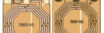
18 Fabrication The device can be mounted directly on a PCB or laminate substrate using conventional wire-bonding techniques. RF test board layout shows an UWB band-pass-filter with 3 with bonds to input pad (#3) and output pad (#6). The four ground pads (#1, #2, #4, #5) are also connected with triple wire bonds pads. G-S-G G patterns on the test board Figure 10: UWB band-pass-filter wire-bond die and RF test board layout. 18
19 UWB Band-Pass-Filter for Wire Bonding IPD The characteristics of the UWB band-pass-filter of wire bonding die are shown in Figure 11. The insertion loss is 2.4dB (Minimum) and the return loss is 7dB. Compared to the results for the flip chip UWB filter, these results are much worse than expected. Insertio on Loss (db B) Insertion Loss Return Loss (db) Return Loss Frequency (GHz) Frequency (GHz) Figure 11: Measured characteristics of the UWB band-pass-filter of wire bonding die. 19
20 Tripe wire-bond inductance model Figure 12 shows a comparison of the simulated result versus measurement using the simple triple wire bond inductance model. The simple model does not account for mutual interactions between the wire bonds, which become more important at higher frequencies. It can be seen that the agreement between the two is poor. Because of the good agreement in the flipchip case, it was suspected the cause of the discrepancy was in the simple inductance model used for the wire bonds. (S 11,S 21 db) S 21 db) e WB model data ( rement data (S 11, Simple Measu Simple WB model data Measurement data Frequency (GHz) Figure 12: Measurement versus simulation using the simple triple wire-bond inductance models for wire-bonding IPD. 20
21 Wire-bond shape model BONDW_Shape Shape1 Rw=12.5 um Gap=700 um StartH=250 um MaxH=350 um Tilt=50 um Stretch=100 um StopH=0 um FlipX=1 Top figure applies StartH is 250um (top of IPD) StopH is 0 (plane of the test board) Gap is 700um (total length of the wire bond in the x-y plane) MaxH is 350um (a 100um loop height typical.) Tilt and stretch are chosen to give the wire bond a reasonable shape. 21


22 Simulation setup This is the same as the simple model, but the wire-bond inductors have been replaced by the ADS WIRESET model. Term Term1 Num=1 Z=50 Ohm Term Term2 Num=2 Z=50 Ohm pad_1 pad_2 pad_3 pad_4 pad_5 pad_6 BONDW18 WIRESET1 Radw=12.5 um Cond=1.3e7 S View=side Layer="cond" SepX=0 um SepY=0 um Zoffset=0 um W1_Shape="Shape1" BONDW_Shape Shape1 Rw=12.5 um Gap=700 um StartH=250 um MaxH=350 um Tilt=50 um Stretch=100 um StopH=0 um FlipX=1 S-PARAMETERS S_Param SP1 Start=0.01 GHz Stop=15 GHz Step=5 MHz pad_1 pad_2 pad_ Ref pad_6 pad_5 pad_4 S6P SNP1 File="UWB_8GHZ_3WB_FINAL_runit_1_1.s6p" FINAL it 1 " W2_Zoffset=0 um W5_Zoffset=0 um W8_Zoffset=0 um W11_Zoffset=0 um W14_Zoffset=0 um W17_Zoffset=0 um W2_Angle=180 W5_Angle=180 W8_Angle=90 W11_Angle=90 W14_Angle=0 W17_Angle=0 W3_Shape="Shape1" W6_Shape="Shape1" W9_Shape="Shape1" W12_Shape="Shape1" W15_Shape="Shape1" W18_Shape="Shape1" W3_Xoffset=-465 um W6_Xoffset=-465 um W9_Xoffset=-285 um W12_Xoffset=465 um W15_Xoffset=465 um W18_Xoffset=465 um W3_Yoffset=-185 um W6_Yoffset=180 um W9_Yoffset=365 um W12_Yoffset=365 um W15_Yoffset=0 um W18_Yoffset=-365 um W3_Zoffset=0 um W6_Zoffset=0 um W9_Zoffset=0 um W12_Zoffset=0 um W15_Zoffset=0 um W18_Zoffset=0 um W3_Angle=180 W6_Angle=180 W9_Angle=90 W12_Angle=90 W15_Angle=0 W18_Angle=0 W4_Shape="Shape1" W7_Shape="Shape1" W10_Shape="Shape1" W13_Shape="Shape1" W16_Shape="Shape1" W1_Xoffset=-465 um W4_Xoffset=-465 um W7_Xoffset=-465 um W10_Xoffset=285 um W13_Xoffset=465 um W16_Xoffset=465 um W1_Yoffset=-365 um W4_Yoffset=0 um W7_Yoffset=365 um W10_Yoffset=365 um W13_Yoffset=180 um W16_Yoffset=-185 um W1_Zoffset=0 um W4_Zoffset=0 um W7_Zoffset=0 um W10_Zoffset=90 um W13_Zoffset=0 um W16_Zoffset=0 um W1_Angle=180 W4_Angle=180 W7_Angle=90 W10_Angle=0 W13_Angle=0 W16_Angle=0 W2_Shape="Shape1" W5_Shape="Shape1" W8_Shape="Shape1" W11_Shape="Shape1" W14_Shape="Shape1" W17_Shape="Shape1" W2_Xoffset=-465 um W5_Xoffset=-465 um W8_Xoffset=-375 um W11_Xoffset=375 um W14_Xoffset=465 um W17_Xoffset=465 um W2_Yoffset=-275 um W5_Yoffset=90 um W8_Yoffset=365 um W11_Yoffset=365 um W14_Yoffset=90 um W17_Yoffset=-275 um Wires labeled 1-18 counter-clockwise 1 18 Wires labeled 1-18 counter-clockwise 22
23 Tripe wire-bond inductance model An improved circuit-level simulation was done using the Philips /TU Delft wire-bond models in ADS. These account for a more detailed shape of the wire bond and also account for mutual inductances between all of the wires. The comparison between the IPD characteristics using the simple triple wire bond model and the more accurate Philips/TU Delft model is shown in Figure 13. Figure 13: Simulation using the simple triple wire-bond inductance model versus simulation using the Philips/TU Delft triple wire bond inductance models. data (S 11, S 21 db) a (S 11, S 21 db) mple WB model d S WB model data Sim ADS Frequency (GHz) Simple WB model data ADS WB model data
24 Tripe wire-bond inductance model Figure 14 shows a comparison of the measured data versus simulation using the Philips TU/Delft wire-bond inductance model for wire-bond IPD. With the more accurate wire-bond models, the agreement is much better. At these high frequencies, the simple wire-bond models are not sufficiently accurate. db) 1 db) Measuremen nt data ( S 11, S 21 ADS WB mod del data (S 11, S Measurement data ADS WB model data Frequency (GHz) Figure 14: Measurement versus simulation using the Philips/TU Delft triple wire-bond inductance models. 24
25 Conclusions The design and implementation of a silicon based band-pass-filter for Ultra Wide Band applications have been presented. Excellent filter properties are obtained from the UWB band-passfilter of flip-chip die. For wire bondable IPDs working at high frequencies (such as this UWB filter), simple inductance model for multiple wires is not good enough for designs. More advanced coupled-wire models in ADS have shown better predictions of the wire behaviors. The IPD technology is especially well suited for UWB applications because of its excellent parameter control and enabling smaller from-factors. factors 25
Integrated Passive Device (IPD) Technology for Wireless Applications
 Technology for Wireless Applications") Ultra-Wide-Band (UWB) Band-Pass-Filter Using Integrated Passive Device (IPD) Technology for Wireless Applications June 17, 2009 STATS ChipPAC D&C YongTaek Lee Rev01 Agenda Introduction Design and characterization
Ultra-Wide-Band (UWB) Band-Pass-Filter Using Integrated Passive Device (IPD) Technology for Wireless Applications June 17, 2009 STATS ChipPAC D&C YongTaek Lee Rev01 Agenda Introduction Design and characterization
High Rejection BPF for WiMAX Applications from Silicon Integrated Passive Device Technology
 High Rejection BPF for WiMAX Applications from Silicon Integrated Passive Device Technology by Kai Liu, Robert C Frye* and Billy Ahn STATS ChipPAC, Inc, Tempe AZ, 85284, USA, *RF Design Consulting, LLC,
Innovations in EDA Webcast Series
 Welcome Innovations in EDA Webcast Series August 2, 2012 Jack Sifri MMIC Design Flow Specialist IC, Laminate, Package Multi-Technology PA Module Design Methodology Realizing the Multi-Technology Vision
Session 4: Mixed Signal RF
 Sophia Antipolis October 5 th & 6 th 2005 Session 4: Mixed Signal RF Technology, Design and Manufacture of RF SiP Chris Barratt, Michel Beghin, Insight SiP Insight SiP Summary Introduction Definition of
A passive circuit based RF optimization methodology for wireless sensor network nodes. Article (peer-reviewed)
") Title Author(s) Editor(s) A passive circuit based RF optimization methodology for wireless sensor network nodes Zheng, Liqiang; Mathewson, Alan; O'Flynn, Brendan; Hayes, Michael; Ó Mathúna, S. Cian Wu,
Title Author(s) Editor(s) A passive circuit based RF optimization methodology for wireless sensor network nodes Zheng, Liqiang; Mathewson, Alan; O'Flynn, Brendan; Hayes, Michael; Ó Mathúna, S. Cian Wu,
DESIGN OF COMPACT MICROSTRIP LOW-PASS FIL- TER WITH ULTRA-WIDE STOPBAND USING SIRS
 Progress In Electromagnetics Research Letters, Vol. 18, 179 186, 21 DESIGN OF COMPACT MICROSTRIP LOW-PASS FIL- TER WITH ULTRA-WIDE STOPBAND USING SIRS L. Wang, H. C. Yang, and Y. Li School of Physical
INSIGHT SiP. RF System in Package, design methodology and practical examples of highly integrated systems
 INSIGHT SiP RF System in Package, design methodology and practical examples of highly integrated systems Chris Barratt Insight SiP Sophia Antipolis France 1 RF SiP Technologies PRD Design Methodology Initial
Design and Analysis of Novel Compact Inductor Resonator Filter
 Design and Analysis of Novel Compact Inductor Resonator Filter Gye-An Lee 1, Mohamed Megahed 2, and Franco De Flaviis 1. 1 Department of Electrical and Computer Engineering University of California, Irvine
SiP packaging technology of intelligent sensor module. Tony li
 SiP packaging technology of intelligent sensor module Tony li 2016.9 Contents What we can do with sensors Sensor market trend Challenges of sensor packaging SiP technology to overcome challenges Overview
Optimization Design and Simulation for a Band- Pass-Filter with IPD Technology for RF Front-end Application
 Optimization Design and Simulation for a Band- Pass-Filter with IPD Technology for RF Front-end Application Huijuan Wang 1,2,*, Jie Pan 1,2, Xiaoli Ren 1, Anmou Liao 1,2,Yuan Lu 1,2, Daquan Yu 2, Dongkai
Optimal design methodology for RF SiP - from project inception to volume manufacturing
 Optimal design methodology for RF SiP - from project inception to volume manufacturing Chris Barratt Insight SiP 905 rue Albert Einstein Valbonne France 06560 Outline RF SiP Technologies Design Methodology
A TUNABLE GHz BANDPASS FILTER BASED ON SINGLE MODE
 Progress In Electromagnetics Research, Vol. 135, 261 269, 2013 A TUNABLE 1.4 2.5 GHz BANDPASS FILTER BASED ON SINGLE MODE Yanyi Wang *, Feng Wei, He Xu, and Xiaowei Shi National Laboratory of Science and
ENGAT00000 to ENGAT00010
 Wideband Fixed Attenuator Family, DIE, DC to 50 GHz ENGAT00000 / 00001 / 00002 / 00003 / 00004 / 00005 / 00006 / 00007 / 00008 / 00009 / 00010 Typical Applications ENGAT00000 to ENGAT00010 Features Space
The 3D Silicon Leader
 The 3D Silicon Leader 3D Silicon IPD for smaller and more reliable Implantable Medical Devices ATW on Advanced Packaging for Wireless Medical Devices Mohamed Mehdi Jatlaoui, Sébastien Leruez, Olivier Gaborieau,
Operation of Microwave Precision Fixed Attenuator Dice up to 40 GHz
 Operation of Microwave Precision Fixed Attenuator Dice up to 40 GHz (AN-70-019) I. INTRODUCTION Mini-Circuits YAT-D-series MMIC attenuator dice (RoHS compliant) are fixed value, absorptive attenuators
CMD282. DC-40 GHz 2-bit Digital Attenuator. Features. Functional Block Diagram. Description
 Features Functional Block Diagram Ultra wideband performance Low insertion loss Wide attenuation range Small die size Description The CMD282 is negative controlled, wideband GaAs MMIC 2-bit digital attenuator
LTCC Components. ShenZhen Sunlord Electronics CO., LTD.
 LTCC Components Content 1 The concept of LTCC About LTCC technology 2 Sunlord LTCC components Multilayer chip Antenna Multilayer chip Filter Multilayer chip Diplexer Multilayer chip Balun Multilayer chip
Managing Complex Impedance, Isolation & Calibration for KGD RF Test Abstract
 Managing Complex Impedance, Isolation & Calibration for KGD RF Test Roger Hayward and Jeff Arasmith Cascade Microtech, Inc. Production Products Division 9100 SW Gemini Drive, Beaverton, OR 97008 503-601-1000,
A Simple Bandpass Filter with Independently Tunable Center Frequency and Bandwidth
 Progress In Electromagnetics Research Letters, Vol. 69, 3 8, 27 A Simple Bandpass Filter with Independently Tunable Center Frequency and Bandwidth Bo Zhou *, Jing Pan Song, Feng Wei, and Xiao Wei Shi Abstract
T est POST OFFICE BOX 1927 CUPERTINO, CA TEL E P H ONE (408) FAX (408) ARIES ELECTRONICS
 FAX (408) ARIES ELECTRONICS") G iga T est L abs POST OFFICE BOX 1927 CUPERTINO, CA 95015 TEL E P H ONE (408) 524-2700 FAX (408) 524-2777 ARIES ELECTRONICS BGA SOCKET (0.80MM TEST CENTER PROBE CONTACT) Final Report Electrical Characterization
G iga T est L abs POST OFFICE BOX 1927 CUPERTINO, CA 95015 TEL E P H ONE (408) 524-2700 FAX (408) 524-2777 ARIES ELECTRONICS BGA SOCKET (0.80MM TEST CENTER PROBE CONTACT) Final Report Electrical Characterization
A COMPACT DUAL-BAND POWER DIVIDER USING PLANAR ARTIFICIAL TRANSMISSION LINES FOR GSM/DCS APPLICATIONS
 Progress In Electromagnetics Research Letters, Vol. 1, 185 191, 29 A COMPACT DUAL-BAND POWER DIVIDER USING PLANAR ARTIFICIAL TRANSMISSION LINES FOR GSM/DCS APPLICATIONS T. Yang, C. Liu, L. Yan, and K.
Multilayer Organic (MLO TM )
") HOW TO ORDER DP 03 C 1580 Type Size Design Frequency (MHz) QUALITY INSPECTION 1 6 1 6 1 6 2 5 2 5 2 5 3 4 3 4 3 4 MLO TM TECHNOLOGY Finished parts are 100% tested for electrical parameters and visual characteristics.
HOW TO ORDER DP 03 C 1580 Type Size Design Frequency (MHz) QUALITY INSPECTION 1 6 1 6 1 6 2 5 2 5 2 5 3 4 3 4 3 4 MLO TM TECHNOLOGY Finished parts are 100% tested for electrical parameters and visual characteristics.
Evaluation of Package Properties for RF BJTs
 Application Note Evaluation of Package Properties for RF BJTs Overview EDA simulation software streamlines the development of digital and analog circuits from definition of concept and estimation of required
Data Sheet. ACFF-1024 ISM Bandpass Filter ( MHz) Description. Features. Specifications. Functional Block Diagram.
 Description. Features. Specifications. Functional Block Diagram.") ACFF-124 ISM Bandpass Filter (241 2482 MHz) Data Sheet Description The Avago ACFF-124 is a miniaturized Bandpass Filter designed for use in the 2.4 GHz Industrial, Scientific and Medical (ISM) band. The
ACFF-124 ISM Bandpass Filter (241 2482 MHz) Data Sheet Description The Avago ACFF-124 is a miniaturized Bandpass Filter designed for use in the 2.4 GHz Industrial, Scientific and Medical (ISM) band. The
Application Note 1330
 HMPP-3865 MiniPAK PIN Diode High Isolation SPDT Switch Design for 1.9 GHz and 2.45 GHz Applications Application Note 133 Introduction The Avago Technologies HMPP-3865 parallel diode pair combines low inductance,
77 GHz VCO for Car Radar Systems T625_VCO2_W Preliminary Data Sheet
 77 GHz VCO for Car Radar Systems Preliminary Data Sheet Operating Frequency: 76-77 GHz Tuning Range > 1 GHz Output matched to 50 Ω Application in Car Radar Systems ESD: Electrostatic discharge sensitive
Upper UWB Interference Free Filter Using Dumb- Bell Resonator and Vias
 Upper UWB Interference Free Filter Using Dumb- Bell Resonator and Vias 1 Dr.H.Umma Habiba, 2 M.Aishwarya, 3 Kavyashri Parameswaran, 4 Minakshy.R, 5 Mohit Jhunjhunwala 1 Professor, 2,3,4,5 Research Scholars
COMPACT DUAL-MODE TRI-BAND TRANSVERSAL MICROSTRIP BANDPASS FILTER
 Progress In Electromagnetics Research Letters, Vol. 26, 161 168, 2011 COMPACT DUAL-MODE TRI-BAND TRANSVERSAL MICROSTRIP BANDPASS FILTER J. Li 1 and C.-L. Wei 2, * 1 College of Science, China Three Gorges
Gain Equalizers EQY-SERIES. Microwave. The Big Deal
 Microwave Gain Equalizers 50Ω DC to GHz EQY-SERIES The Big Deal Excellent Return Loss, 0dB typ. Wide bandwidth, DC - GHz Small Size, mm x mm CASE STYLE: MC131-1 Product Overview EQY series of absorptive
Data Sheet. ACFF-1025 LTE Band 41 Bandpass Filter. Features. Description. Specifications. Functional Block Diagram. Applications
 ACFF-125 LTE Band 41 Bandpass Filter Data Sheet Description The Avago ACFF-125 is a highly miniaturized LTE Band 41 (2496 269 MHz) bandpass filter combined with a WLAN/Wi-Fi band reject filter. The ACFF-125
A NOVEL MICROSTRIP LC RECONFIGURABLE BAND- PASS FILTER
 Progress In Electromagnetics Research Letters, Vol. 36, 171 179, 213 A NOVEL MICROSTRIP LC RECONFIGURABLE BAND- PASS FILTER Qianyin Xiang, Quanyuan Feng *, Xiaoguo Huang, and Dinghong Jia School of Information
REFLECTIONLESS FILTER DICE
 MMIC REFLECTIONLESS FILTER DICE 50Ω DC to 21 GHz The Big Deal Patented design eliminates in band spurs Pass band cut-off up to 21 GHz Stop band up to 35 GHz Excellent repeatability through IPD* process
Design of Duplexers for Microwave Communication Systems Using Open-loop Square Microstrip Resonators
 International Journal of Electromagnetics and Applications 2016, 6(1): 7-12 DOI: 10.5923/j.ijea.20160601.02 Design of Duplexers for Microwave Communication Charles U. Ndujiuba 1,*, Samuel N. John 1, Taofeek
Physical RF Circuit Techniques and Their Implications on Future Power Module and Power Electronic Design
 Physical RF Circuit Techniques and Their Implications on Future Power Module and Power Electronic Design Adam Morgan 5-5-2015 NE IMAPS Symposium 2015 Overall Motivation Wide Bandgap (WBG) semiconductor
Model BD1631J50100AHF
 Model BD1631J51AHF Ultra Low Profile 85 Balun 5Ω to 1Ω Balanced Description The BD1631J51AHF is a low profile sub-miniature balanced to unbalanced transformer designed for differential inputs and output
GHz Voltage Variable Attenuator (Absorptive)
") Rev.. February 27.5-2.GHz Voltage Variable Attenuator (Absorptive) Features Single Positive Voltage Control: to +5V. 3dB Attenuation Range Low Insertion Loss I/O VSWR
Rev.. February 27.5-2.GHz Voltage Variable Attenuator (Absorptive) Features Single Positive Voltage Control: to +5V. 3dB Attenuation Range Low Insertion Loss I/O VSWR
Anaren 0805 (B0809J50ATI) balun optimized for Texas Instruments CC1100/CC1101 Transceiver
 balun optimized for Texas Instruments CC1100/CC1101 Transceiver") (ANN-2005) Rev B Page 1 of 13 Anaren 0805 (B0809J50ATI) balun optimized for Texas Instruments CC1100/CC1101 Transceiver Trong N Duong RF Co-Op Nithya R Subramanian RF Engineer Introduction The tradeoff
(ANN-2005) Rev B Page 1 of 13 Anaren 0805 (B0809J50ATI) balun optimized for Texas Instruments CC1100/CC1101 Transceiver Trong N Duong RF Co-Op Nithya R Subramanian RF Engineer Introduction The tradeoff
PART MAX2605EUT-T MAX2606EUT-T MAX2607EUT-T MAX2608EUT-T MAX2609EUT-T TOP VIEW IND GND. Maxim Integrated Products 1
 19-1673; Rev 0a; 4/02 EVALUATION KIT MANUAL AVAILABLE 45MHz to 650MHz, Integrated IF General Description The are compact, high-performance intermediate-frequency (IF) voltage-controlled oscillators (VCOs)
CHAPTER 7 CONCLUSION AND FUTURE WORK
 132 CHAPTER 7 CONCLUSION AND FUTURE WORK 7.1 CONCLUSION In this research, UWB compact BPFs, single and dual notch filters, reconfigurable filter are developed in microstrip line using PCB technology. In
A unique 3D Silicon Capacitor with outstanding performances in terms of DC leakage and reliability performances. Catherine Bunel R&D Director
 A unique 3D Silicon Capacitor with outstanding performances in terms of DC leakage and reliability performances. Catherine Bunel R&D Director Agenda Introduction Ipdia core technology Application overview
Hardware Design Considerations for MKW41Z/31Z/21Z BLE and IEEE Device
 NXP Semiconductors Document Number: AN5377 Application Note Rev. 2, Hardware Design Considerations for MKW41Z/31Z/21Z BLE and IEEE 802.15.4 Device 1. Introduction This application note describes Printed
Design Considerations for Highly Integrated 3D SiP for Mobile Applications
 Design Considerations for Highly Integrated 3D SiP for Mobile Applications FDIP, CA October 26, 2008 Joungho Kim at KAIST joungho@ee.kaist.ac.kr http://tera.kaist.ac.kr Contents I. Market and future direction
CMY210. Demonstration Board Documentation / Applications Note (V1.0) Ultra linear General purpose up/down mixer 1. DESCRIPTION
 Ultra linear General purpose up/down mixer 1. DESCRIPTION") Demonstration Board Documentation / (V1.0) Ultra linear General purpose up/down mixer Features: Very High Input IP3 of 24 dbm typical Very Low LO Power demand of 0 dbm typical; Wide input range Wide LO
Demonstration Board Documentation / (V1.0) Ultra linear General purpose up/down mixer Features: Very High Input IP3 of 24 dbm typical Very Low LO Power demand of 0 dbm typical; Wide input range Wide LO
TCP-3182H. 8.2 pf Passive Tunable Integrated Circuits (PTIC)
") TCP-3182H 8.2 pf Passive Tunable Integrated Circuits (PTIC) Introduction ON Semiconductor s PTICs have excellent RF performance and power consumption, making them suitable for any mobile handset or radio
TCP-3182H 8.2 pf Passive Tunable Integrated Circuits (PTIC) Introduction ON Semiconductor s PTICs have excellent RF performance and power consumption, making them suitable for any mobile handset or radio
Monolithic Amplifier Die
 Flat Gain, Ultra-Wideband Monolithic Amplifier Die 50Ω 0.01 to 12 GHz The Big Deal Ultra broadband performance Outstanding Gain flatness, ±0.7 db over 0.05 to 6 GHz Broadband high dynamic range without
Chapter 6. Case Study: 2.4-GHz Direct Conversion Receiver. 6.1 Receiver Front-End Design
 Chapter 6 Case Study: 2.4-GHz Direct Conversion Receiver The chapter presents a 0.25-µm CMOS receiver front-end designed for 2.4-GHz direct conversion RF transceiver and demonstrates the necessity and
Synthesis of Optimal On-Chip Baluns
 Synthesis of Optimal On-Chip Baluns Sharad Kapur, David E. Long and Robert C. Frye Integrand Software, Inc. Berkeley Heights, New Jersey Yu-Chia Chen, Ming-Hsiang Cho, Huai-Wen Chang, Jun-Hong Ou and Bigchoug
Application Note 5446
 Design the Avago MGA-31T6 into a High Gain, Low Noise, Low current GPS LNA Module Application Note 446 Introduction The MGA-31T6 is a low cost and easy-to-use GaAs LNA (Low Noise Amplifier). The LNA is
Rf Low Pass Filter Design And Fabrication Using Integrated Passive Device Technology
 University of Central Florida Electronic Theses and Dissertations Masters Thesis (Open Access) Rf Low Pass Filter Design And Fabrication Using Integrated Passive Device Technology 2006 Heli Li University
1 FUNDAMENTAL CONCEPTS What is Noise Coupling 1
 Contents 1 FUNDAMENTAL CONCEPTS 1 1.1 What is Noise Coupling 1 1.2 Resistance 3 1.2.1 Resistivity and Resistance 3 1.2.2 Wire Resistance 4 1.2.3 Sheet Resistance 5 1.2.4 Skin Effect 6 1.2.5 Resistance
Dual-band LNA Design for Wireless LAN Applications. 2.4 GHz LNA 5 GHz LNA Min Typ Max Min Typ Max
 Dual-band LNA Design for Wireless LAN Applications White Paper By: Zulfa Hasan-Abrar, Yut H. Chow Introduction Highly integrated, cost-effective RF circuitry is becoming more and more essential to the
RF Board Design for Next Generation Wireless Systems
 RF Board Design for Next Generation Wireless Systems Page 1 Introduction Purpose: Provide basic background on emerging WiMax standard Introduce a new tool for Genesys that will aide in the design and verification
MSPP Page 1. MSPP Competencies in SiP Integration for Wireless Applications
 MSPP Page 1 MSPP Competencies in SiP Integration for Wireless Applications MSPP Page 2 Outline Design, simulation and measurements tools MSPP competencies in electrical design and modeling Embedded passive
Low Noise Amplifier Design Methodology Summary By Ambarish Roy, Skyworks Solutions, Inc.
 February 2014 Low Noise Amplifier Design Methodology Summary By Ambarish Roy, Skyworks Solutions, Inc. Low Noise Amplifiers (LNAs) amplify weak signals received by the antenna in communication systems.
Data Sheet. VMMK GHz E-pHEMT Wideband Amplifier in Wafer Level Package. Description. Features. Specifications (6GHz, 5V, 25mA Typ.
 VMMK-223.9-11 GHz E-pHEMT Wideband Amplifier in Wafer Level Package Data Sheet Description Avago Technologies has combined its industry leading E-pHEMT technology with a revolutionary wafer level package
Using Analyst TM to Quickly and Accurately Optimize a Chip-Module-Board Transition
 Using Analyst TM to Quickly and Accurately Optimize a Chip-Module-Board Transition 36 High Frequency Electronics By Dr. John Dunn 3D electromagnetic Optimizing the transition (EM) simulators are commonly
NPA100-D GHz GaN 20W Power Amplifier. Product Description: Key Features:
 Product Description: The Nxbeam is a Ku-band high power GaN MMIC fabricated in 0.2um GaN HEMT on SiC. This part is ideally suited for satellite communications, point-to-point radios, and radar applications.
Flip-Chip for MM-Wave and Broadband Packaging
 1 Flip-Chip for MM-Wave and Broadband Packaging Wolfgang Heinrich Ferdinand-Braun-Institut für Höchstfrequenztechnik (FBH) Berlin / Germany with contributions by F. J. Schmückle Motivation Growing markets
COMPACT TRI-LAYER ULTRA-WIDEBAND BAND- PASS FILTER WITH DUAL NOTCH BANDS
 Progress In Electromagnetics Research, Vol. 106, 49 60, 2010 COMPACT TRI-LAYER ULTRA-WIDEBAND BAND- PASS FILTER WITH DUAL NOTCH BANDS P.-Y. Hsiao and R.-M. Weng Department of Electrical Engineering National
Flexible Hybrid Electronics Fabricated with High-Performance COTS ICs using RTI CircuitFilm TM Technology
 Flexible Hybrid Electronics Fabricated with High-Performance COTS ICs using RTI CircuitFilm TM Technology Scott Goodwin 1, Erik Vick 2 and Dorota Temple 2 1 Micross Advanced Interconnect Technology Micross
Progress In Electromagnetics Research, Vol. 107, , 2010
 Progress In Electromagnetics Research, Vol. 107, 101 114, 2010 DESIGN OF A HIGH BAND ISOLATION DIPLEXER FOR GPS AND WLAN SYSTEM USING MODIFIED STEPPED-IMPEDANCE RESONATORS R.-Y. Yang Department of Materials
FEATURES DESCRIPTION ABSOLUTE MAXIMUM RATINGS. T AMB = +25 C ( Unless otherwise specified )
") Monolithic PIN SP5T Diode Switch FEATURES Ultra Broad Bandwidth: 50MHz to 26GHz 1.0 db Insertion Loss 30 db Isolation at 20GHz Reliable. Fully Monolithic Glass Encapsulated Construction DESCRIPTION The
Monolithic PIN SP5T Diode Switch FEATURES Ultra Broad Bandwidth: 50MHz to 26GHz 1.0 db Insertion Loss 30 db Isolation at 20GHz Reliable. Fully Monolithic Glass Encapsulated Construction DESCRIPTION The
HMC1044LP3E. Programmable Harmonic Filters - SMT. Functional Diagram. General Description
 Typical Applications The HMC144LP3E is ideal for wideband transceiver harmonic filtering applications including: Filtering lo Harmonics to Reduce Modulator Sideband Rejection & Demodulator Image Rejection
Chapter 2. Literature Review
 Chapter 2 Literature Review 2.1 Development of Electronic Packaging Electronic Packaging is to assemble an integrated circuit device with specific function and to connect with other electronic devices.
Design of a BAW Quadplexer Module Using NI AWR Software
 Application Note Design of a BAW Quadplexer Module Using NI AWR Software Overview With the development of the LTE-Advanced and orthogonal frequency division multiple access (OFDMA) techniques, multiple
Analysis and design of lumped element Marchand baluns
 Downloaded from orbit.dtu.d on: Mar 14, 218 Analysis and design of lumped element Marchand baluns Johansen, Tom Keinice; Krozer, Vitor Published in: 17th International Conference on Microwaves, Radar and
A novel output transformer based highly linear RF-DAC architecture Bechthum, E.; Radulov, G.I.; Briaire, J.; Geelen, G.; van Roermund, A.H.M.
 A novel output transformer based highly linear RF-DAC architecture Bechthum, E.; Radulov, G.I.; Briaire, J.; Geelen, G.; van Roermund, A.H.M. Published in: Proceedings of the 2st European Conference on
Data Sheet. VMMK GHz Variable Gain Amplifier in SMT Package. Features. Description. Specifications (6 GHz, Vdd = 5 V, Zin = Zout = 50 Ω)
") VMMK-. - 18 GHz Variable Gain Amplifier in SMT Package Data Sheet Description The VMMK- is a small and easy-to-use, broadband, variable gain amplifier operating in various frequency bands from.-18 GHz.
VMMK-. - 18 GHz Variable Gain Amplifier in SMT Package Data Sheet Description The VMMK- is a small and easy-to-use, broadband, variable gain amplifier operating in various frequency bands from.-18 GHz.
DISTRIBUTED amplification is a popular technique for
 IEEE TRANSACTIONS ON CIRCUITS AND SYSTEMS II: EXPRESS BRIEFS, VOL. 58, NO. 5, MAY 2011 259 Compact Transformer-Based Distributed Amplifier for UWB Systems Aliakbar Ghadiri, Student Member, IEEE, and Kambiz
High-Selectivity UWB Filters with Adjustable Transmission Zeros
 Progress In Electromagnetics Research Letters, Vol. 52, 51 56, 2015 High-Selectivity UWB Filters with Adjustable Transmission Zeros Liang Wang *, Zhao-Jun Zhu, and Shang-Yang Li Abstract This letter proposes
Inductor Modeling of Integrated Passive Device for RF Applications
 Inductor Modeling of Integrated Passive Device for RF Applications Yuan-Chia Hsu Meng-Lieh Sheu Chip Implementation Center Department of Electrical Engineering 1F, No.1, Prosperity Road I, National Chi
IF Digitally Controlled Variable-Gain Amplifier
 19-2601; Rev 1; 2/04 IF Digitally Controlled Variable-Gain Amplifier General Description The high-performance, digitally controlled variable-gain amplifier is designed for use from 0MHz to 400MHz. The
Search. Login Register. Patrick Gormally -March 24, 2014
 EDN MOMENT Space Shuttle Columbia is delivered, March 25, 1979 Search Login Register Patrick Gormally -March 24, 2014 Share Tweet 0 Like 0 Over the years medical devices have continually been made smaller;
INVENTION DISCLOSURE- ELECTRONICS SUBJECT MATTER IMPEDANCE MATCHING ANTENNA-INTEGRATED HIGH-EFFICIENCY ENERGY HARVESTING CIRCUIT
 INVENTION DISCLOSURE- ELECTRONICS SUBJECT MATTER IMPEDANCE MATCHING ANTENNA-INTEGRATED HIGH-EFFICIENCY ENERGY HARVESTING CIRCUIT ABSTRACT: This paper describes the design of a high-efficiency energy harvesting
GaAs Flip Chip Schottky Barrier Diodes MA4E1317, MA4E1318, MA4E1319-1, MA4E V1. Features. Description and Applications MA4E1317
 Features Low Series Resistance Low Capacitance High Cutoff Frequency Silicon Nitride Passivation Polyimide Scratch Protection Designed for Easy Circuit Insertion Description and Applications M/A-COM's
COMPACT ULTRA-WIDEBAND BANDPASS FILTER WITH DEFECTED GROUND STRUCTURE
 Progress In Electromagnetics Research Letters, Vol. 4, 25 31, 2008 COMPACT ULTRA-WIDEBAND BANDPASS FILTER WITH DEFECTED GROUND STRUCTURE M. Shobeyri andm. H. VadjedSamiei Electrical Engineering Department
Data Sheet. ACMD-7402 Miniature PCS Band Duplexer. Description. Features. Specifications. Applications. Functional Block Diagram
 ACMD-742 Miniature PCS Band Duplexer Data Sheet Description The Avago ACMD-742 is a miniature duplexer designed for US PCS handsets. The ACMD-742 is designed with Avago Technologies Film Bulk Acoustic
The Challenges of Differential Bus Design
 The Challenges of Differential Bus Design February 20, 2002 presented by: Arthur Fraser TechKnowledge Page 1 Introduction Background Historically, differential interconnects were often twisted wire pairs
MMIC: Introduction. Evangéline BENEVENT. Università Mediterranea di Reggio Calabria DIMET
 Evangéline BENEVENT Università Mediterranea di Reggio Calabria DIMET 1 Evolution of electronic circuits: high frequency and complexity Moore s law More than Moore System-In-Package System-On-Package Applications
Monolithic Amplifier Die
 Ultra High Dynamic Range Monolithic Amplifier Die 50Ω 0.05 to 1.5 GHz The Big Deal Ultra High IP3 Broadband High Dynamic Range without external Matching Components Product Overview (RoHS compliant) is
EVALUATION KIT AVAILABLE 3.5GHz Downconverter Mixers with Selectable LO Doubler. PART MAX2683EUE MAX2684EUE *Exposed pad TOP VIEW IFOUT+ IFOUT-
 -; Rev ; / EVALUATION KIT AVAILABLE.GHz Downconverter Mixers General Description The MAX/MAX are super-high-performance, low-cost downconverter mixers intended for wireless local loop (WLL) and digital
Design of UWB Bandpass Filter with WLAN Band Rejection by DMS in Stub Loaded Microstrip Highpass Filter
 Design of UWB Bandpass Filter with WLAN Band Rejection by DMS in Stub Loaded Microstrip Highpass Filter Pratik Mondal 1, Hiranmoy Dey *2, Arabinda Roy 3, Susanta Kumar Parui 4 Department of Electronics
Power Reduction in RF
 Power Reduction in RF SoC Architecture using MEMS Eric Mercier 1 RF domain overview Technologies Piezoelectric materials Acoustic systems Ferroelectric materials Meta materials Magnetic materials RF MEMS
ABA GHz Broadband Silicon RFIC Amplifier. Application Note 1349
 ABA-52563 3.5 GHz Broadband Silicon RFIC Amplifier Application Note 1349 Introduction Avago Technologies ABA-52563 is a low current silicon gain block RFIC amplifier housed in a 6-lead SC 70 (SOT- 363)
SHELLCASE-TYPE WAFER-LEVEL PACKAGING SOLUTIONS: RF CHARACTERIZATION AND MODELING
 SHELLCASE-TYPE WAFER-LEVEL PACKAGING SOLUTIONS: RF CHARACTERIZATION AND MODELING M Bartek 1, S M Sinaga 1, G Zilber 2, D Teomin 2, A Polyakov 1, J N Burghartz 1 1 Delft University of Technology, Lab of
Monolithic Amplifier CMA-103+ Ultra Linear Low Noise, Ceramic to 4 GHz
 Ultra Linear Low Noise, Ceramic Monolithic Amplifier 50Ω 0.05 to 4 GHz The Big Deal Ceramic, hermetically sealed, nitrogen filled Low profile case, 0.045 Ultra High IP3 Broadband High Dynamic Range CASE
NPA105-D. Preliminary GHz GaN 40W Power Amplifier. Product Description: Key Features:
 Product Description: The Nxbeam is a Ku-band high power GaN MMIC fabricated in 0.2um GaN HEMT on SiC. This part is ideally suited for satellite communications, point-to-point radios, and radar applications.
Through Glass Via (TGV) Technology for RF Applications
 Technology for RF Applications") Through Glass Via (TGV) Technology for RF Applications C. H. Yun 1, S. Kuramochi 2, and A. B. Shorey 3 1 Qualcomm Technologies, Inc. 5775 Morehouse Dr., San Diego, California 92121, USA Ph: +1-858-651-5449,
Through Glass Via (TGV) Technology for RF Applications C. H. Yun 1, S. Kuramochi 2, and A. B. Shorey 3 1 Qualcomm Technologies, Inc. 5775 Morehouse Dr., San Diego, California 92121, USA Ph: +1-858-651-5449,
Band Pass Filter Die. XBF-D-Series. Reflectionless to 20.5 GHz
 NEW! Four Section Models Reflectionless Band Pass Filter Die 50Ω 15.5 to 20.5 GHz XBF-D-Series The Big Deal High Stopband rejection, up to 77 db Patented design terminates stopband signals Stop band up
Enabling High Parallelism in Production RF Test
 Enabling High Parallelism in Production RF Test Patrick Rhodes Ryan Garrison Ram Lakshmanan FormFactor Connectivity is Driving Change The connected world is driving the growth of RFICs in the market. These
Design of Compact Stacked-Patch Antennas in LTCC multilayer packaging modules for Wireless Applications
 Design of Compact Stacked-Patch Antennas in LTCC multilayer packaging modules for Wireless Applications R. L. Li, G. DeJean, K. Lim, M. M. Tentzeris, and J. Laskar School of Electrical and Computer Engineering
Data Sheet. VMMK GHz Positive Gain Slope Low Noise Amplifier in SMT Package. Features. Description
 VMMK-3603 1-6 GHz Positive Gain Slope Low Noise Amplifier in SMT Package Data Sheet Description The VMMK-3603 is a small and easy-to-use, broadband, positive gain slope low noise amplifier operating in
IEEE Antennas and Wireless Propagation Letters. Copyright Institute of Electrical and Electronics Engineers.
 Title Dual-band monopole antenna with frequency-tunable feature for WiMAX applications Author(s) Sun, X; Cheung, SW; Yuk, TTI Citation IEEE Antennas and Wireless Propagation Letters, 2013, v. 12, p. 100-103
Microwave Metrology -ECE 684 Spring Lab Exercise T: TRL Calibration and Probe-Based Measurement
 ab Exercise T: TR Calibration and Probe-Based Measurement In this project, you will measure the full phase and magnitude S parameters of several surface mounted components. You will then develop circuit
ATF-531P8 900 MHz High Linearity Amplifier. Application Note 1372
 ATF-531P8 9 MHz High Linearity Amplifier Application Note 1372 Introduction This application note describes the design and construction of a single stage 85 MHz to 9 MHz High Linearity Amplifier using
Advanced Wafer Level Packaging of RF-MEMS with RDL Inductor
 Advanced Wafer Level Packaging of RF-MEMS with RDL Inductor Paul Castillou, Roberto Gaddi, Rob van Kampen, Yaojian Lin*, Babak Jamshidi** and Seung Wook Yoon*** Cavendish Kinetics, 2960 North First Street,
Accurate Simulation of RF Designs Requires Consistent Modeling Techniques
 From September 2002 High Frequency Electronics Copyright 2002, Summit Technical Media, LLC Accurate Simulation of RF Designs Requires Consistent Modeling Techniques By V. Cojocaru, TDK Electronics Ireland
Fixed Attenuator Die YAT-D-SERIES. The Big Deal Excellent power handling, up to 2W Wideband, DC to 26.5 GHz Usable to 40 GHz
 Microwave Precision Fixed Attenuator Die 50Ω Up to 2W DC to 26.5 GHz YAT-D-SERIES The Big Deal Excellent power handling, up to 2W Wideband, DC to 26.5 GHz Usable to 40 GHz Unpackaged die form Product Overview
BANDPASS CAVITY RESONATORS
 BANDPASS CAVITY RESONATORS S Parameters Measurements and Modelling Using Bandpass Cavities for Impedance Matching Jacques Audet VE2AZX Web: ve2azx.net With the collaboration of Luc Laplante VE2ULU May
S. Jovanovic Institute IMTEL Blvd. Mihaila Pupina 165B, Belgrade, Serbia and Montenegro
 Progress In Electromagnetics Research, PIER 76, 223 228, 2007 MICROSTRIP BANDPASS FILTER AT S BAND USING CAPACITIVE COUPLED RESONATOR S. Prabhu and J. S. Mandeep School of Electrical and Electronic Engineering