Input aperture size (mm) Supply voltage Features Conversion dynode ± 1.
|
|
|
- Bruno Collins
- 6 years ago
- Views:
Transcription
1
 yet low dark current, allowing operation in photon counting mode to detect and measure extremely small incoming particles and")
 and Auger electron spectroscopy")

 (MΩ) 2 7. 2 9. 6 6 One megohm resistor is connected between Dynode and Dynode 2. 2Supply a negative potential to the conversion dynode when detecting positive ions.")
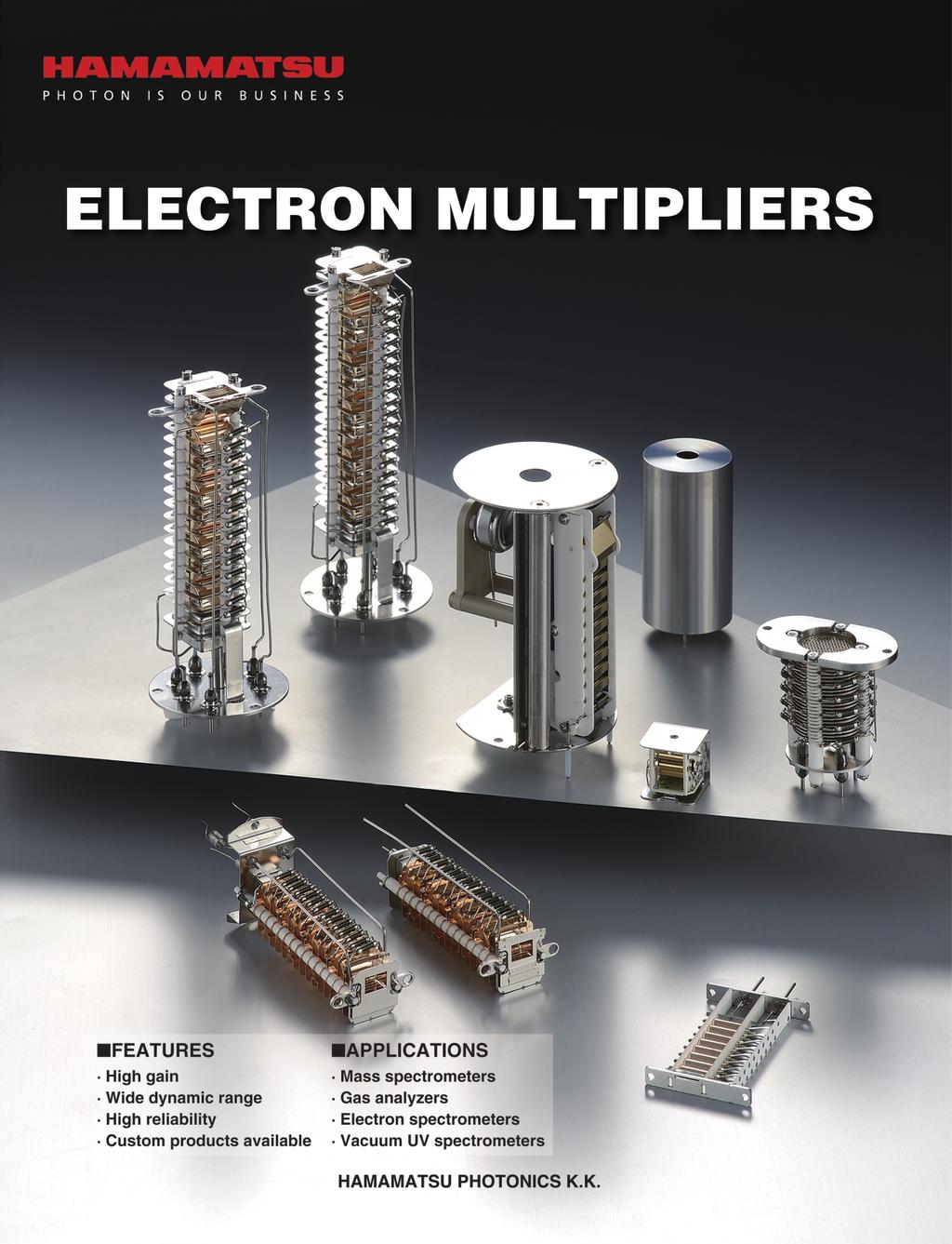
2 PRODUCT LINE-UP Electron multipliers are mainly used as positive/negative ion detectors. They are also useful for detecting and measuring vacuum UV rays and soft X-rays. Hamamatsu electron multipliers have a high gain (multiplication factor) yet low dark current, allowing operation in photon counting mode to detect and measure extremely small incoming particles and their energy. This means our Hamamatsu electron multipliers are ideal for electron spectroscopy and vacuum UV spectroscopy such as ESCA (electron spectroscopy for chemical analysis) and Auger electron spectroscopy as well as mass spectroscopy and field-ion microscopy. Type No. R6- R R88 R262 R0- R7 R R96 R9 Structure Linear-focused Linear-focused Circular-cage Coarse mesh Box-and-line Box-and-grid Box-and-grid Box-and-grid Box-and-grid Dynode Number of stages Material Al2O Al2O Input aperture size (mm) Supply (V) Characteristics Typ. (ns) Typ. (pa) (MΩ) One megohm resistor is connected between Dynode and Dynode 2. 2Supply a negative potential to the conversion dynode when detecting positive ions. Supply a positive potential when detecting negative ions. Gain Typ. Rise time Dark current Detection Total ion resistance polarity 6 20 /negative 2 Anode to all other electrode capacitance (pf) R6- R Thin configuration Can be stacked side-by-side 2.0 ± ± 0.. ± 0. (8 ).0 ± ± ± ± Conversion dynode 8 ±.0 ± 0.2 CONVERS DYNODE ± ± ± 0. 9 ± 2- ± ELECTRON MULTIPLYING SECT 22.0 ± 0. HV PIN ± 0. 2 ± CONVERS DYNODE PIN 2.0 ± ± ± PIN TPMHA088EB 0.0 ± ± 0. TPMHA087EB R88 R262 Small, lightweight Includes Faraday cup Front plate (case): ± 0.2 Wide detection area 20.0 ± ±.0 ± INPUT APERTURE 60 MAX. -. PIN 0 ± 20.0 ± ± ± ± 0. OUTPUT LEAD HV LEAD HV PIN 2 FARADAY CUP LEAD TPMHA0608EA TPMHA0609EA
 200 000 2000 000 0 000 000 000 000 Anode to last dynode (V) 0 0 00 00 Maximum ratings Conversion (kv) ± 2 Faraday cup (V) -200-0 -0 Average")

3 Electron multipliers listed in this catalog are standard products. We welcome requests for custom products. Please contact us with your needs. Operating gain Anode to first dynode (V) Anode to last dynode (V) Maximum ratings Conversion (kv) ± 2 Faraday cup (V) Average anode current (µa) Bake-out temperature - Pa ( C) Operating vacuum level (Pa) Do not perform baking on the R Use a supply that does not cause the operating gain to exceed its maximum rating. Gain characteristics GAIN TPMHB0929EA 2000 SUPPLY VOLTAGE (V) R6- R R88 R262 R0- R7, R, R96 R R0- R7 R Easy handling (contained in a case) Mounting plate potential Shield case: 7 MAX ± 0..0 ± 0..0 ± 0..0 ± ± 0.2 HAMAMATSU -.2 SHIELD CASE 2.0 ± 0. PIN First dynode usable as Faraday cup Mounting plate potential 26.0 ± ± MAX. 8.0 ± ± ± ± 0.2 INPUT APERTURE 2-.2 LEAD LENGTH 90 MIN. SEMI- FLEXIBLE LEAD 2- DY2 PIN HV PIN (DY) First dynode usable as Faraday cup Mounting plate potential HV PIN OUTPUT.0 ± 0. HV (DY) 9 MAX ± MAX. 6.0 ± ± ± ± ± 0. INPUT APERTURE DY TPMHA06EA TPMHA06EA TPMHA062EA R96 R9 Wide detection area 0 MAX. 2.0 ± MAX. 2.0 ± 0.2 ± ± ± 0. High gain Wide detection area 2.0 ± ± MAX. 0 MAX. ± 2.0 ± ± 0. PIN 0 ±.0 ± ± HV PIN (DY) TPMHA06EA PIN 0 ±.0 ± ± HV PIN (DY) TPMHA06EA
4 TECHNICAL INFORMAT CONSTRUCT AND OPERATING PRINCIPLE An electron multiplier mainly consists of a input aperture, an electron multiplying section (dynode section), an anode, and -divider resistors. Electron multipliers operate in a vacuum and guide the particles or rays (positive/negative ions, vacuum UV rays, soft X-rays, etc.) so as to enter the first dynode. The first dynode is excited by such particles or rays and emits secondary electrons from its surface. These electrons are multiplied in cascade by the second and following dynodes and a cluster of secondary electrons finally reaches the anode and is output as a signal. ELECTRON MULTIPLYING SECT Electron multipliers operate with a high S/N ratio since they have low noise and high gain. This low noise and high gain is achieved by an electron multiplying section made up of to 2 stages of electrodes called dynodes. Before using an electron multiplier, it is first exposed to air once and then installed in equipment. The dynode therefore uses materials that exhibit stable characteristics and less deterioration even when exposed to air. Hamamatsu electron multipliers are designed and produced based on our advanced technology for photomultiplier tubes and so have high performance. The dynode structures in the electron multiplying section are described below. ) Box-and-grid type This type consists of a train of quarter cylindrical dynodes and offers good electron collection efficiency and excellent uniformity. This type is likely to resist breakdown even DYNODE : -HV DYNODE DYNODE 2 2) Circular-cage type The circular-cage type features a compact design and fast time response. DYNODE 7 ANODE: DYNODE 8 FARADAY CUP TPMHC02EA ) Box-and-line type The structure of this type consists of a combination of box-and-grid and linear-focus dynodes. This type offers better time response than the boxand-grid type and higher ion collection efficiency than the linear-focused type. ) Coarse mesh type This type has a structure of wire dynodes with a triangle cross section stacked in the form of a mesh. This structure ensures excellent linearity and is less affected by magnetic fields. Compared to other dynode structures this type makes it easier to design a detector with a wider effective area. CONVERS DYNODE (CD) The acceleration of ions differs according to their mass. The speed at which ions enter the first dynode affects the secondary electron emission efficiency, so the higher the speed, the better the efficiency. When detecting ions with a large mass (for example, polymer compounds), the ions must be accelerated by a high potential to obtain a speed great enough to maintain a sufficient secondary electron emission efficiency. Conversion dynodes (CD) are usually used to give a high potential to such ions with a large mass. SENSITIVITY RATIO TPMHB09EA Sample: Per fluore tri-buthyl amine Sensitivity of electron multiplier with conversion dynode Sensitivity ratio = Sensitivity of electron multiplier mm TPMHC026EA TPMHC027EA MASS/CHARGE RATIO (m/z) ) Linear-focused type The linear-focused type exhibits fast time response and has a thin configuration that is easy to design and use. Because of these advantages the linear-focused type is frequently used in magnetic field deflection mass spectrometers where multiple detectors need to be installed side-by-side. MAGNET HEAVY LIGHT -00 V ELECTRON MULTIPLIER (R6-) SIGNAL SIGNAL TPMHC02EA TPMHC026EA THICKNESS: 6 mm SENSITIVITY Electron multipliers can be used to detect and measure ions, vacuum UV rays, soft X-rays, and other rays by selecting a particular material for the first dynode. ) Ions When one ion enters and strikes the first dynode, multiple electrons are emitted from the first dynode. The number of the emitted electrons depends on the mass of the ion and the acceleration. The figure below shows how the electron emission ratio depends on the acceleration when detecting nitrogen ions. ELECTRON EMISS RATIO TPMHB0927EA SOURCE TPMHC029EA 2 ACCELERAT VOLTAGE (V)
5 2) Light Hamamatsu electron multipliers use beryllium copper oxide () or aluminum oxide (Al2O) for the first dynode. Beryllium copper oxide is sensitive to soft X-rays to UV light at around 00 nm. Depending on the wavelength incident on the first dynode or the usage, the first dynode can be replaced with a dynode on which an alkali-halide material is deposited. This gives the first dynode spectral response characteristics starting from just a few nanometers. ) Electrons The material used for the first dynode also has sensitivity to electrons having an energy level exhibited by Auger electrons, secondary electrons, and reflection electrons. The figure below shows the relation between the primary-electron acceleration for beryllium copper oxide and aluminum oxide and the secondary electron emission ratio. The secondary electron emission ratio is at a maximum when the primary-electron acceleration is about 00 V to 00 V. SECONDARY ELECTRON EMISS RATIO TPMHB0928EA 6 2 ALUMINUM OXIDE (Al2O) BERYLLIUM COPPER OXIDE () PRIMARY-ELECTRON ACCELERAT VOLTAGE (V) GAIN The gain of an electron multiplier is given by the following equation: Gain (µ) = A Ebb kn A : constant Ebb: supply k : value determined by electrode structure and material n : number of dynode stages This equation reveals that the gain (µ) is proportional to the supply. The figure below shows how the gain of typical electron multipliers varies with the supply. Block diagram for gain measurement ELECTRON MULTIPLIER HIGH VOLTAGE POWER SUPPLY PREAMP AMMETER PULSE HEIGHT ANALYZER TPMHC028EA If an oscilloscope is used, the gain can be calculated by the "area of output pulse waveform (charge amount) divided by the elementary charge." When using an electron multiplier equipped with a Faraday cup, the gain can also be expressed as the ratio of the anode output current after multiplication by dynode to the input current to the Faraday cup. DARK CURRENT AND NOISE The beryllium copper oxide and aluminum oxide used for the secondary emissive surface of dynodes have a high work function and so exhibit exceptionally low dark current and noise. Dark current and noise may be generated by the following three factors: Thermionic electrons are emitted from secondary electron emissive surface of dynode 2Leakage current from dynode support materials Field emission electron current of dynode Hamamatsu electron multipliers have dark current of about pa when supply providing a gain of 6. SOURCE NOISE In some mass spectrometers, an ion source, analyzer, and ion detector are arrayed in a straight line. The ion source ionizes a sample but at the same time generates UV light and X-rays. These UV light and X-rays will cause noise if they pass through the analyzer and enter the electron multiplier. This noise is referred to as "ion source noise". To reduce this noise component, the first dynode or conversion dynode is arranged at a position slightly offset from the ion input aperture and an electric field lens created by a special electrode is used to allow only the sample ions to enter the first dynode or conversion dynode. This is called an "off-axis structure". The figure below shows the ion detection mechanism of an off-axis electron multiplier. TPMHB0929EA 8 7 GAIN SUPPLY VOLTAGE (V) R6- R R88 R262 R0- R7, R, R96 R The circuit system shown in the following block diagram can be used to measure the gain of an electron multiplier operating under single ion input conditions. The pulse height analyzer measures the total number of counts per second; and the ammeter measures the output current value under the same conditions. The gain is then calculated by "output current/elementary charge/number of counts per second." NOISE SOURCE (UV light, X-rays etc.) Q-POLE Q-POLE FARADAY CUP -00 V ELECTRODE TPMHC029EA VACUUM LEVEL AND NOISE The vacuum level affects the generation of noise in an electron multiplier. The noise is usually low at a vacuum level for example of - Pa, but increases as the vacuum level drops for example to 0. Pa. We recommend operating the electron multiplier at a vacuum level higher than about -2 Pa although the level may depend on the operating gain and the type of detector.
6 TECHNICAL INFORMAT DC LINEARITY Electron multipliers are shipped with a -divider circuit assembled inside. The current that will flow in the -divider circuit can be calculated by the total resistance of the divider circuit divided by the supply. The relation between the input ion energy and the average anode current maintains an ideal linearity in a certain energy range. However, as the input energy increases or the amount of input ions increases, the output current also increases and becomes saturated near the value of the current flowing in the -divider circuit. To maintain the ideal linearity, we recommend regulating the average anode current to /20th or less of the current flowing in the -divider circuit. To achieve a high counting efficiency, it is necessary to choose a linear-focused-dynode electron multiplier that has fast time response and a -divider circuit with lower total resistance. However, please note that the -divider circuit is likely to generate more heat as the resistance is lowered. LIFE CHARACTERISTICS The lifetime of electron multipliers is usually affected by the operating gain, output current and the operating vacuum level. The following three factors are the main limits on the lifetime. Deterioration in the first dynode or conversion dynode by incident ions 2Deterioration in the secondary electron emission capability of dynodes near the last stage, which is caused by collision of large amounts of electrons Contamination adhering to the secondary emissive surface We conducted in-house testing by operating our electron multipliers under conditions where residual gases (carbon) are present and analyzed the results. Larger amounts of carbon deposits were detected on the latter dynode stages where the electron density was high, so we think that the contamination (residual gases, etc.) inside the analyzer (especially the vacuum chamber) has a significant effect on the lifetime. Also, unlike photomultiplier tubes, electron multipliers are not completely sealed and so may possibly be exposed to surrounding gases, moisture, oil or grease and other items during storage, causing deterioration in the characteristics. CONNECT METHODS The inter-electrode is supplied through a -divider circuit made up of resistors connected in series. The connection methods are described below according to the polarity of the ions to detect. ion detection As shown in the figure below, the input aperture and the last dynode are grounded and a negative high is supplied to the first dynode during operation. +HV and +HV2 creates a difference in potential. The last dynode is connected to the anode via resistor, and a coupling capacitor is connected to the anode to prevent the positive high from being input to the externally connected measuring device. This means that DC signals cannot be extracted by this measurement method. NEGATIVE ion detection using electron multiplier with conversion dynode When measuring positive ions, a negative high (about - kv) is supplied to the conversion dynode, another negative high is applied to the first dynode, and the last dynode is grounded. ions are converted into electrons by the conversion dynode. POSITIVE +HV CONVERS DYNODE: - kv DY: -HV ELECTRON LAST STAGE: TPMHC026EA TPMHC0262EA Negative ion detection using electron multiplier with conversion dynode When measuring negative ions, a positive high (about + kv) is supplied to the conversion dynode, a negative high is applied to the first dynode, and the last dynode is grounded. Negative ions are converted into positive ions by the conversion dynode and the positive ions are then converted into electrons by the first dynode. DY +HV2 CONVERS DYNODE: + kv ANODE COUPLING CAPACITOR POSITIVE DY ANODE NEGATIVE POSITIVE ELECTRON 6 -HV TPMHC0260EA 2Negative ion detection As the following figure shows, the input opening is grounded, a positive high (+HV) is supplied to the first dynode to draw negative ions, and another positive high (+HV2) to the last dynode. The difference in between DY: -HV LAST STAGE: TPMHC026EA Faraday cup Hamamatsu also provides electron multipliers equipped with a Faraday cup function. The Faraday cup function and electron multiplying function cannot be used simultaneously. If a high is supplied to the electron multiplying section while operating the Faraday cup, the incoming ions shift their trajectories toward the electron multiplying section and so fail to reach the Faraday cup.
7 6Dual-mode electron multiplier Dual mode allows both the analog output and pulse output to be measured with just one detector. As the figure below shows, the analog output is measured at an intermediate stage of the electron multiplying section while the pulse output is measured at the last stage. INPUT APERTURE TPMHC026EA When the amount of ions is very small, a pulse output function which provides high gain is used to count the output pulses. When the amount of ions is large, the analog output with low gain is used to make measurement. This prevents the detector from being saturated and allows measurements ranging from a small to a large quantity of ions. As seen from the figure below, a wide dynamic range of 9 orders of magnitude can be obtained. ANODE COUNT RATE (s - ) -HV TPMHB090EA ANALOG OUTPUT DY COUNTING SIGNAL ANALOG SIGNAL GATE PULSED OUTPUT We are fully capable of developing and producing dual-mode electron multipliers to meet special customer requests. +HV RELATIVE INPUT COUPLING CAPACITOR ANALOG OUTPUT CURRENT (A) SAFETY PRECAUTS High is used to operate an electron multipliers and related products. When using these products, provide adequate safety measures by taking precautions to prevent operators and workers from receiving electrical shocks as well as equipment damage. HANDLING PRECAUTS () An electron multiplier consists of electrodes and substrates that are precision-assembled. Applying excessive force or shock might deform them and cause faulty operation. Handle the electron multipliers as carefully as possible. (2) Electron multipliers are shipped in packages filled with nitrogen (N2) gas. Those packages are intended for use during shipping and are not suited for long-term storage. When storing an electron multiplier, keep it in a clean case under either of the following conditions a) and b), even before unpacking and also after unpacking. a) Store in a clean case at a vacuum pressure below Pa and isolated much as possible from oil or grease. b) Store in a clean case where dry nitrogen flows constantly while passed through a 0. µm or smaller filter (humidity: 20 % or less). () When using an electron multiplier and its peripheral parts for the first time or when re-operating after storage, perform vacuum baking or carry out degassing under high vacuum conditions (at a pressure below -2 Pa) for more than 2 hours before attempting operation. () Vacuum baking cannot be performed on some types of electron multipliers depending on what materials are used or how they are processed. Please consult us for detailed information before attempting vacuum baking. After performing vacuum baking on an electron multiplier do not attempt to operate it until its temperature decreases to 0 C or less. () When installing an electron multiplier in equipment, take the following precautions: Wear clean powder-free nylon or polyethylene gloves and do not handle with bare hands. When wiring to the electron multiplier keep the leads at least mm away from other metallic parts. To prevent abnormal discharges, do not bring any pointed objects close to the electron multiplier. Use a shielded cable for the signal cable that connects the anode output to an amplifier and subsequent device. The shielded cable should be as short as possible. (6) Each electron multiplier must be operated at a vacuum level higher than the maximum operating vacuum level. If operated at a lower vacuum level the residual gas molecules might discharge or light emissions might occur, leading to fatal damage to the electron multiplier. (7) Do not operate any of the electron multipliers at a gain or supply higher than specified. Operation at a higher gain or supply may promote deterioration of the gain, increase the output drift and noise, and degrade the linearity. (8) Do not draw a higher output current than necessary. Excessive output current may impair the signal linearity and degrade the life characteristics. OTHERS () We are constantly making every effort to improve product quality and reliability but this does not guarantee the safety of electron multipliers. When using an electron multiplier in equipment where there is a risk of death, injury, or damage to property, please be sure to provide appropriate safety design and measures that take potential problems fully into account. (2) When giving instructions to the end user about how to use electron multipliers or the equipment used along with an electron multiplier, please explain the functions, performance, and correct handling of the electron multiplier and equipment, as well as appropriate warnings and displays, etc. 7
8 WARRANTY As a general rule, Hamamatsu electron multipliers and their related products are warranted for a period of one year from the date of delivery. The warranty is limited to replacement of defective products. However, the warranty shall not apply to the following cases and you will be charged for replacement of the product. () Malfunction or damage was caused by incorrect use or modification. (2) Malfunction or damage was caused by natural or man-made disasters, or other inevitable accidents. WHEN DISPOSE THE PRODUCT When disposing of an electron multiplier, take appropriate measures in compliance with applicable regulations regarding waste disposal and correctly dispose of it yourself, or entrust proper disposal to a licensed industrial waste disposal company. In any case, be sure to comply with the regulations in your country or state to ensure correct disposal. Subject to local technical requirements and regulations, availability of products included in this promotional material may vary. Please consult with our sales office. Information furnished by HAMAMATSU is believed to be reliable. However, no responsibility is assumed for possible inaccuracies or omissions. Specifications are subject to change without notice. No patent rights are granted to any of the circuits described herein. 20 Hamamatsu Photonics K.K. HAMAMATSU PHOTONICS K.K. HAMAMATSU PHOTONICS K.K., Electron Tube Division -, Shimokanzo, Iwata City, Shizuoka Pref., 8-09, Japan, Telephone: (8)9/62-28, Fax: (8)9/ U.S.A.: Hamamatsu Corporation: 60 Foothill Road, Bridgewater. N.J , U.S.A., Telephone: () , Fax: () usa@hamamatsu.com Germany: Hamamatsu Photonics Deutschland GmbH: Arzbergerstr., D-822 Herrsching am Ammersee, Germany, Telephone: (9)82-7-0, Fax: (9) info@hamamatsu.de France: Hamamatsu Photonics France S.A.R.L.: 9, Rue du Saule Trapu, Parc du Moulin de Massy, 9882 Massy Cedex, France, Telephone: () , Fax: () infos@hamamatsu.fr United Kingdom: Hamamatsu Photonics UK Limited: 2 Howard Court, Tewin Road, Welwyn Garden City, Hertfordshire AL7 BW, United Kingdom, Telephone: () , Fax: () info@hamamatsu.co.uk North Europe: Hamamatsu Photonics Norden AB: Torshamnsgatan SE-6 0 Kista, Sweden, Telephone: (6) , Fax: (6) info@hamamatsu.se Italy: Hamamatsu Photonics Italia S.r.l.: Strada della Moia, int. 6, Arese (Milano), Italy, Telephone: (9)02-987, Fax: (9) info@hamamatsu.it TPMHE0 China: Hamamatsu Photonics (China) Co., Ltd.: B20 Jiaming Center, No.27 Dongsanhuan Beilu, Chaoyang District, Beijing 0020, China, Telephone: (86) , Fax: (86) hpc@hamamatsu.com.cn JUN. 20 IP
5 W XENON FLASH LAMP MODULES
 LAMP W XENON FLASH LAMP MODULES : L/L series (side-on type) : L/L series (head-on type) : L/L series (high output type) : L (SMA fiber adapter type) : L/L series (high precision type) : L/L series (silent
XENON FLASH LAMP MODULES
 LAMP COMPACT W MODULES : L/L series (side-on type) : L/L series (head-on type) : L/L series (high output type) : L (SMA fiber adapter type) : L/L series (high precision type) : L/L series (silent type)
Compact SMD type high output LED
 Compact SMD type high output LED The is a small-size LED available in a surface mount COB package. Its size is drastically reduced compared to the previous premolded type. Features Applications High output
High power LED, peak emission wavelength: 1.45 µm
 High power LED, peak emission wavelength:.45 µm The is a high-power LED that emits infrared light at a peak of.45 µm. A bullet-shaped package () and a surface mount type () are available. It offers high
InGaAs PIN photodiodes
 Long wavelength type (cutoff wavelength: 2.05 to 2.1 μm) Features Cutoff wavelength: 2.05 to 2.1 μm Low cost Photosensitive area: φ0.3 to φ3 mm Low noise High sensitivity High reliability High-speed response
InGaAs PIN photodiodes
 Long wavelength type (cutoff wavelength: 2.55 to 2.6 μm) Features Cutoff wavelength: 2.55 to 2.6 μm Low cost Photosensitive area: φ0.3 to φ3 mm Low noise High sensitivity High reliability High-speed response
InGaAs PIN photodiodes
 area from ϕ0.3 mm to ϕ5 mm InGaAs PIN photodiodes have large shunt resistance and feature very low noise. Hamamatsu provides various types of InGaAs PIN photodiodes with photosensitive area from ϕ0.3 mm
InAs photovoltaic detectors
 P9 series P763 Low noise, high reliability infrared detectors (for 3 µm band) InAs photovoltaic detectors have high sensitivity in the infrared region around 3 µm as with PbS photoconductive detectors,
Energy saving sensors for TV brightness controls, etc.
 S7184 Linear current amplification of photodiode output The and S7184 consist of a photodiode and a signal processing circuit for amplifying the photocurrent generated from the photodiode up to 1300 times.
Photo IC diode. Wide operating temperature: -40 to +105 C. S MT. Absolute maximum ratings
 Wide operating temperature: -40 to +05 C The photo IC has a spectral response close to human eye sensitivity. Two active areas are made on a single chip. Almost only the visible range can be measured by
Radiation detection modules
 C7 series High accuracy, high sensitivity, compact radiation detection module The C7 series is a radiation detection module containing a scintillator and MPPC (multi-pixel photon counter) designed to detect
InAs photovoltaic detectors
 P9 series P763 Low noise, high reliability infrared detectors (for 3 μm band) InAs photovoltaic detectors have high sensitivity in the infrared region around 3 μm as with PbS photoconductive detectors,
InGaAs PIN photodiodes
 area from ϕ0.3 mm to ϕ5 mm InGaAs PIN photodiodes have large shunt resistance and feature very low noise. Hamamatsu provides various types of InGaAs PIN photodiodes with photosensitive area from ϕ0.3 mm
TECHNICAL INFORMATION. How to Use UVTRON
 TECHNICAL INFORMATION How to Use The is a sensor sensitive only to ultraviolet light with wavelengths shorter than 26 nm. Featuring high sensitivity high output, and high-speed response, the is the ideal
Si photodiodes with preamp
 Si photodiodes with preamp Photodiode and preamp integrated with feedback resistance and capacitance The and are low-noise sensors consisting of Si photodiode, op amp, and feedback resistance and capacitance,
Si photodiodes with preamp
 Si photodiodes with preamp Photodiode and preamp integrated with feedback resistance and capacitance The and are low-noise sensors consisting of Si photodiode, op amp, and feedback resistance and capacitance,
MEMS-FPI spectrum sensor
 Ultra-compact near infrared spectrum sensor that integrates MEMS tunable filter and photosensor The MEMS-FPI spectrum sensor is a ultra-compact sensor that houses a MEMS-FPI (Fabry-Perot Interferometer)
PHOTOMULTIPLIER TUBE MODULES, NEW RELEASED PAMPHLET
 PHOTOMULTIPLIER TUBE MODULES, NEW RELEASED PAMPHLET This pamphlet is gathered up the new released products from January 9. Photomultiplier tube (PMT) module functions are shown in the chart below. PMT
MIRROR QE=0.1 % MIRROR
 MICROCHANNEL PLATE- PHOTOMULTIPLIER TUBES (MCP-PMT) SERIES FEATURES High Speed Rise Time: 160 ps IRF (Instrument Response Function) A : 55 ps (FWHM) Low Noise Compact Profile Useful Photocathode: 11 mm
Photo IC diodes S SB S CT. Spectral response close to human eye sensitivity. Absolute maximum ratings (Ta=25 C)
") Photo IC diodes S9066-211SB S9067-201CT Spectral response close to human eye sensitivity The S9066-211SB, S9067-201CT photo ICs have spectral response close to human eye sensitivity. Two photosensitive
Photo IC diodes S9066-211SB S9067-201CT Spectral response close to human eye sensitivity The S9066-211SB, S9067-201CT photo ICs have spectral response close to human eye sensitivity. Two photosensitive
CMOS linear image sensor
 RGB color image sensor The is a CMOS linear image sensor that is sensitive to red (630 nm), green (540 nm), and blue (460 nm). Filters are attached to the pixels in the following order: R, G, and B. Features
Applications S S S S 1024
 IMAGE SENSOR NMOS linear image sensor S9/S9 series Built-in thermoelectric cooler ensures long exposure time and stable operation. NMOS linear image sensors are self-scanning photodiode arrays designed
CMOS linear image sensors
 CMOS linear image sensors S12198 series (-01) Smoothly varying spectral response characteristics in UV region The S12198 series are CMOS linear image sensors using a vertically long pixels (25 500 µm).
CMOS linear image sensor
 Achieves high sensitivity by adding an amplifier to each pixel The is a CMOS linear image sensor that achieves high sensitivity by adding an amplifier to each pixel. It has a long photosensitive area (effective
Mini-spectrometers. TM series. High sensitivity type (integrated with backthinned type CCD image sensor) C10082CA/C10083CA series
 C10082CA/C10083CA series") C12CA/C13CA series High sensitivity type (integrated with backthinned type CCD ) mini-spectrometers are polychromators integrated with optical elements, an and a driver circuit. Light to be measured is
C12CA/C13CA series High sensitivity type (integrated with backthinned type CCD ) mini-spectrometers are polychromators integrated with optical elements, an and a driver circuit. Light to be measured is
GATED MICROCHANNEL PLATE PHOTOMULTIPLIER TUBES (MCP-PMT) R5916U-50 SERIES
 R5916U-50 SERIES") PHOTOMULTIPLIER TUBES (MCP-PMT) SERIES FEATURES High Speed Gating by Low Supply Voltage (+10 V) Gate Rise Time : 1 ns A Gate Width : 3 ns Fast Rise Time : 180 ps Narrow T.T.S. B : 90 ps High Switching
PHOTOMULTIPLIER TUBES (MCP-PMT) SERIES FEATURES High Speed Gating by Low Supply Voltage (+10 V) Gate Rise Time : 1 ns A Gate Width : 3 ns Fast Rise Time : 180 ps Narrow T.T.S. B : 90 ps High Switching
Digital Cameras for Microscopy
 Digital Cameras for Microscopy Fast frame rate and high sensitivity EM-CCD (Electron multiplication CCD) cameras High dynamic range Enhanced Ideal format for short exposures, fast frame rate and high dynamic
LCOS-SLM (Liquid Crystal on Silicon - Spatial Light Modulator)
") POWER LCOS-SLM CONTROLLER RESET POWER OUTPUT ERROR LCOS-SLM (Liquid Crystal on Silicon - Spatial Light Modulator) Control your light! Shape your beam! Improve your image! The devices are a reflective type
POWER LCOS-SLM CONTROLLER RESET POWER OUTPUT ERROR LCOS-SLM (Liquid Crystal on Silicon - Spatial Light Modulator) Control your light! Shape your beam! Improve your image! The devices are a reflective type
CMOS linear image sensor
 CMOS linear image sensor S11639-01 High sensitivity, photosensitive area with vertically long pixels The S11639-01 is a high sensitivity CMOS linear image sensor using a photosensitive area with vertically
CMOS linear image sensors
 CMOS linear image sensors S10121 to S10124 series (-01) Higher UV sensitivity than previous type, current-output type sensors with variable integration time function The S10121 to S10124 series are self-scanning
01 12-bit digital output
 12-bit digital output The is a digital color sensor sensitive to red (λ=615 nm), green (λ=540 nm) and blue (λ=465 nm) regions of the spectrum. Detected signals are serially output as 12-bit digital data.
Photodiode arrays with amplifiers
 Photodiode arrays with amplifiers S3885 series Photodiode arrays combined with signal processing IC for X-ray detection The S3885 series are photodiode arrays with amplifiers having a phosphor sheet attached
PMA-12. Photonic multichannel analyzer. Scientific applications. Industrial applications. UV to visible spectroscopy. Fluorescence spectroscopy
 Photonic multichannel analyzer Scientific applications UV to visible spectroscopy Fluorescence spectroscopy Raman scattering Chemiluminescence analysis Liquid chromatography Gas chromatography ICP emission
CCD linear image sensor
 CCD linear image sensor S11151-2048 High sensitivity in the ultraviolet region, front-illuminated CCD Despite a front-illuminated CCD, the S11151-2048 offers high sensitivity in the ultraviolet region
Enhanced near infrared sensitivity: QE=40% (λ=1000 nm)
") IR-enhanced CCD image sensors Enhanced near infrared sensitivity: QE=40% (λ=1000 nm) The is a family of FFT-CCD image sensors for photometric applications that offer improved sensitivity in the near infrared
IR-enhanced CCD image sensors Enhanced near infrared sensitivity: QE=40% (λ=1000 nm) The is a family of FFT-CCD image sensors for photometric applications that offer improved sensitivity in the near infrared
Photodiode arrays with ampli er
 Photodiode array combined with signal processing IC The S8866-64 and S8866-128 are Si photodiode arrays combined with a signal processing IC chip. The signal processing IC chip is formed by CMOS process
Photodiode arrays with amplifiers
 S865-64G/-8G/-56G S866-64G-0/-8G-0 Photodiode arrays combined with signal processing IC for X-ray detection These are photodiode arrays with an amplifier and a phosphor sheet attached to the photosensitive
Photodiode arrays with amplifiers
 S865-64/-8/-56 S866-64-0/-8-0 Photodiode arrays combined with signal processing IC These are Si photodiode arrays combined with a signal processing IC chip. The signal processing IC chip is formed by CMOS
Quantum Cascade Laser
 Quantum Cascade Laser Front: QCLs Back: Set-up examples with exclusive accessories Quantum Cascade Lasers are semiconductor lasers that offer peak emission in the mid-ir range (4 µm to 10 µm). They have
Photodiode arrays with amplifiers
 S865-64/-28/-256 S866-64-02/-28-02 Photodiode arrays combined with signal processing IC The S865/S866 series are Si photodiode arrays combined with a signal processing IC chip. X-ray tolerance has been
CCD linear image sensor
 CCD linear image sensor S11151-2048 High sensitivity in the ultraviolet region, front-illuminated CCD Despite a front-illuminated CCD, the S11151-2048 offers high sensitivity in the ultraviolet region
Photodiode arrays with amplifier
 /-28/-256 S8866-64-02/-28-02 Photodiode array combined with signal processing IC The /-28/-256 and S8866-64-02/-28-02 are Si photodiode arrays combined with a signal processing IC chip. The signal processing
CMOS linear image sensors
 Built-in electronic shutter function and gain switching function The is a CMOS linear image sensor with electronic shutter function and gain switching function. The has a pixel pitch that is one-half that
Technical note EM-CCD CAMERA. 1. Introduction
 EM-CCD CAMERA Technical note 1. Introduction 2. Technologies of cooled CCD cameras 2.1 Hermetic vacuum-sealed chamber 2.2 Advantages of an Interline Transfer CCD (ER-150 CCD) 2.3 Readout noise 2.4 Dark
CCD image sensors. Improved etaloning characteristics, High-speed type and low noise type available. S11071/S series
 Improved etaloning characteristics, High-speed type and low noise type available The are back-thinned CCD image sensors designed for spectrometers. Two types consisting of a high-speed type (S11071 series)
Applications. active pixels [mm (H) mm(v)] S9979 Non-cooled
![Applications. active pixels [mm (H) mm(v)] S9979 Non-cooled](/thumbs/89/98944635.jpg "Applications. active pixels [mm (H) mm(v)] S9979 Non-cooled") IMAGE SENSOR CCD area image sensor S9979 TDI operation / large active area CCD S9979 is a FFT-CCD area image sensor specifically designed for low-light-level detection in scientific applications. In particular,
IMAGE SENSOR CCD area image sensor S9979 TDI operation / large active area CCD S9979 is a FFT-CCD area image sensor specifically designed for low-light-level detection in scientific applications. In particular,
Photosensor with front-end IC
 Near infrared sensor that integrates an InGas photodiode and front-end IC The is a compact optical device that integrates an InGas photodiode and front-end IC. Signal from a photodiode that receives near
CCD image sensors. Improved etaloning characteristics, High-speed type and low noise type available. S11071/S series
 Improved etaloning characteristics, High-speed type and low noise type available The are back-thinned CCD image sensors designed for spectrometers. Two types consisting of a high-speed type (S11071 series)
Wide range of applications from Real time imaging of low light fluorescence to Ultra low light detection
 Electron Multiplier CCD Camera C100-13, -14 Wide range of applications from Real time imaging of low light fluorescence to Ultra low light detection Great Stability High Sensitivity Low Noise High Resolution
CCD area image sensor
 IR-enhanced CCD area image sensor S11500-1007 Enhanced near infrared sensitivity: QE=40% (λ=1000 nm), back-thinned FFT-CCD The S11500-1007 is an FFT-CCD image sensor for photometric applications that offers
TDI-CCD area image sensor
 S8658-01/01F Image sensor with a long, narrow photosensitive area for X-ray imaging The S8658-01 is an front-illuminated FFT-CCD image sensor developed for X-ray imaging. A F (Fiber Optic plate with Scintillator)
Electron Multiplying CCD Camera. series
 Electron Multiplying CCD Camera series Multiply faster R The ImagEM X2 is an extremely versatile camera that quietly delivers 70 frames/s at full frame and up to 1076 frames/s with analog binning and regions
Multiply faster R. 70 frames/s frames/s. Electron Multiplying CCD Camera
 Electron Multiplying CCD Camera Multiply faster R The ImagEM X2 is an extremely versatile camera that quietly delivers 70 frames/s at full frame and up to 1076 frames/s with analog binning and regions
Near infrared/proximity type sensor
 Reflective sensor with InGas photodiode and infrared housed in a compact package This reflective sensor houses an InGas PIN photodiode and 1.45 μm band in a compact package. The irradiates infrared light
CHAPTER 11 HPD (Hybrid Photo-Detector)
") CHAPTER 11 HPD (Hybrid Photo-Detector) HPD (Hybrid Photo-Detector) is a completely new photomultiplier tube that incorporates a semiconductor element in an evacuated electron tube. In HPD operation, photoelectrons
CHAPTER 11 HPD (Hybrid Photo-Detector) HPD (Hybrid Photo-Detector) is a completely new photomultiplier tube that incorporates a semiconductor element in an evacuated electron tube. In HPD operation, photoelectrons
S3922/S3923 series. NMOS linear image sensor. Voltage output type with current-integration readout circuit and impedance conversion circuit.
 IMAGE SENSOR NMOS linear image sensor S39/S393 series Voltage output type with current-integration readout circuit and impedance conversion circuit NMOS linear image sensors are self-scanning photodiode
Applications KMPDC0019EA. S3923 series: a=25 µm, b=20 µm Absolute maximum ratings Parameter Symbol Value
 IMAGE SENSOR NMOS linear image sensor S39/S393 series Voltage output type with current-integration readout circuit and impedance conversion circuit NMOS linear image sensors are self-scanning photodiode
NIR PHOTOMULTIPLIER TUBES AND THEIR APPLICATIONS
 NIR PHOTOMULTIPLIER TUBES AND THEIR APPLICATIONS NIR PMTs (near-infrared photomultiplier tubes) are photodetectors that provide high-speed response and high sensitivity in the near infrared region. These
CCD area image sensors
 CCD area image sensors S814 S811-11 Front-illuminated FFT-CCD for X-ray imaging The S814 is an FFT-CCD image sensor suitable for intra-oral X-ray imaging in dental diagnosis. The S814 has about 2 mega
CMOS linear image sensor
 S3774 High-speed readout (00 klines/s) The S3774 is a CMOS linear image sensor developed for industrial cameras that require high-speed scanning. The columnparallel readout system, which has a readout
Applications. Number of total pixels. Number of active pixels
 IMAGE SENSOR CCD area image sensor S7/S7 series Back-thinned FFT-CCD S7/S7 series is a family of FFT-CCD image sensors specifically designed for low-light-level detection in scientific applications. By
Applications. General ratings Parameter S S S
 IMAGE SENSOR CCD area image sensor S9736 series 52 52 pixels, front-illuminated FFT-CCDs S9736 series is a family of FFT-CCD area image sensors specifically designed for low-light-level detection in scientific
CCD area image sensors
 S7170-0909 S7171-0909-01 512 512 pixels, back-thinned FFT-CCD HAMAMATSU developed MPP (multi-pinned phase) mode back-thinned FFT-CCDs specifically designed for low-light-level detection in scientific applications.
CCD image sensor. High-speed operation, back-thinned FFT-CCD. S9037/S9038 series. Structure
 High-speed operation, back-thinned FFT-CCD The FFT-CCD image sensors were developed for high-speed line scan cameras. Since an on-chip amplifier having a wide bandwidth is used to an image sensor, a pixel
CCD linear image sensors
 S55-048-0 S56-048-0 Back-thinned CCD image sensors with electronic shutter function The S55-048-0 and S56-048-0 are back-thinned CCD linear image sensors with an internal electronic shutter for spectrometers.
Imaging Software Optimized for Image Acquisition and Analysis
 Imaging Software Optimized for Image Acquisition and Analysis HCImage is designed to solve a wide range of imaging applications. It includes an extensive range of image processing tools that can be used
CCD image sensors. Enhanced near infrared sensitivity, Constant element temperature control. S11511 series. Applications.
 Enhanced near infrared sensitivity, Constant element temperature control The is a family of FFT (full frame transfer)-ccd image sensors for photometric applications that offer improved sensitivity in the
TDI-CCD image sensors
 S10201-04-01 S10202-08-01 S10202-16-01 Operating the back-thinned CCD in TDI mode delivers high sensitivity. TDI-CCD image sensers capture clear and bright images even under low-light-level conditions.
Radiation Detection Instrumentation
 Radiation Detection Instrumentation Principles of Detection and Gas-filled Ionization Chambers Neutron Sensitive Ionization Chambers Detection of radiation is a consequence of radiation interaction with
ETP ELECTRON MULTIPLIERS
 ETP ELECTRON MULTIPLIERS Care and Handling A division of Maintenance, Storage, and Handling of ETP Electron Multipliers ETP Electron Multipliers from SGE are incorporated as original equipment in all areas
CHAPTER 9 POSITION SENSITIVE PHOTOMULTIPLIER TUBES
 CHAPTER 9 POSITION SENSITIVE PHOTOMULTIPLIER TUBES The current multiplication mechanism offered by dynodes makes photomultiplier tubes ideal for low-light-level measurement. As explained earlier, there
CCD linear image sensors
 S13255-2048-02 S13256-2048-02 Back-thinned CCD image sensors with electronic shutter function The S13255-2048-02 and S13256-2048-02 are back-thinned CCD linear image sensors with an internal electronic
83092 Photomultiplier Family
 83092 Photomultiplier Family 25.4mm (1-inch) Diameter Ruggedized, 10-Stage End-Window PMTs With High Temperature Na2KSb Bialkali Photocathodes for Geophysical Exploration Designed for High Temperature
C31034 Series Photomultipliers
 C31034 Series Photomultipliers 51mm (2inch) Diameter 11Stage, End Window Quantacon PMTs Typical Cathode Responsivity Small Photocathode Area Luminous (Projected) C31034 : 440 ua/lm 4 mm x 10 mm minimum
ETP ELECTRON MULTIPLIERS
 ETP ELECTRON MULTIPLIERS ] Care and Handling Electron Multipliers division of Maintenance, Storage, and Handling of ETP Electron Multipliers ETP Electron Multipliers from SGE are being used in a growing
CCD area image sensor
 High sensitivity in U region, anti-blooming function included The CCD area image sensor has a back-thinned structure that enables a high sensitivity in the U to visible region as well as a wide dynamic
CHAPTER 3 BASIC OPERATING METHODS OF PHOTOMULTIPLIER TUBES
 CHAPTER 3 BASIC OPERATING METHODS OF PHOTOMULTIPLIER TUBES This section provides the first-time photomultiplier tube users with general information on how to choose the ideal photomultiplier tube (often
Production of HPDs for the LHCb RICH Detectors
 Production of HPDs for the LHCb RICH Detectors LHCb RICH Detectors Hybrid Photon Detector Production Photo Detector Test Facilities Test Results Conclusions IEEE Nuclear Science Symposium Wyndham, 24 th
Quantum Cascade Laser
 Quantum Cascade Laser Front: QCLs Back: Set-up examples with exclusive accessories Quantum Cascade Lasers are semiconductor lasers that offer peak emission in the mid-ir range (4 µm to 10 µm). They have
CCD area image sensor
 Low readout noise, high resolution (pixel size: 12 μm) The is a family of back-thinned FFT-CCD image sensors specifically designed for low-light-level detection in scientific applications. By using the
Figure 1. Physical Photo of AHV24VN3KV1MAW DESCRIPTION
 Figure 1. Physical Photo of FEATURES High precision Full modulation range on output voltage Negative voltage output Linear regulation Shutdown APPLICATIONS This power module,, is designed for achieving
CCD area image sensor
 Back-thinned FFT-CCD The is a family of FFT-CCD image sensors specifically designed for low-light-level detection in scientific applications. By using the binning operation, the can be used as a linear
what is a multiplier? how does a multiplier work? common multiplier applications II. Assembly Type III. Other Design Concerns
 SECTION 13 Multipliers VMI manufactures many high voltage multipliers, most of which are custom designed for specific requirements. The following information provides general information and basic guidance
Photomultiplier & Photodiode User Guide
 Photomultiplier & Photodiode User Guide This User Manual is intended to provide guidelines for the safe operation of Photek PMT Photomultiplier Tubes and Photodiodes. Please contact Sales or visit: www.photek.co.uk
A New Class of Robust Sub-nanosecond TOF Detectors with High Dynamic Range
 A New Class of Robust Sub-nanosecond TOF Detectors with High Dynamic Range Dick Stresau, Kevin Hunter, Wayne Shiels, Peter Raffin and Yair Benari ETP, Sydney, Australia Presented at the 54th ASMS Conference
LINEAR IRRADIATION TYPE UV-LED UNIT. Concentration of optical technology
 LINEAR IRRADIATION TYPE U-LED UNIT Concentration of optical tecnology LINEAR IRRADIATION TYPE U-LED UNIT Offering U-LED ligt sources wit a cluster of potonics tecnology Te LC-L5G U-LED ligt sources ave
Optical NanoGauge / Optical MicroGauge
 Optical Gauge Series Optical NanoGauge / Optical MicroGauge Optical NanoGauge Optical MicroGauge NEW C156 P6 C10178 P10 C11665 P18 C11011 P0 Ultrathin film measurement with high speed Extensibility model
TOSHIBA CCD Linear Image Sensor CCD (charge coupled device) TCD2561D
 TCD2561D") TOSHIBA CCD Linear Image Sensor CCD (charge coupled device) TCD2561D The TCD2561D is a high sensitive and low dark current 5340 elements 4 line CCD color image sensor which includes CCD drive circuit,
TOSHIBA CCD Linear Image Sensor CCD (charge coupled device) TCD2561D The TCD2561D is a high sensitive and low dark current 5340 elements 4 line CCD color image sensor which includes CCD drive circuit,
Physics Laboratory Scattering of Photons from Electrons: Compton Scattering
 RR Oct 2001 SS Dec 2001 MJ Oct 2009 Physics 34000 Laboratory Scattering of Photons from Electrons: Compton Scattering Objective: To measure the energy of high energy photons scattered from electrons in
Scanning electron microscope
 Scanning electron microscope 5 th CEMM workshop Maja Koblar, Sc. Eng. Physics Outline The basic principle? What is an electron? Parts of the SEM Electron gun Electromagnetic lenses Apertures Detectors
CHAPTER 8 PHOTOMULTIPLIER TUBE MODULES
 CHAPTER 8 PHOTOMULTIPLIER TUBE MODULES This chapter describes the structure, usage, and characteristics of photomultiplier tube () modules. These modules consist of a photomultiplier tube, a voltage-divider
Marconi Applied Technologies CCD30-11 Inverted Mode Sensor High Performance CCD Sensor
 Marconi Applied Technologies CCD30-11 Inverted Mode Sensor High Performance CCD Sensor FEATURES * 1024 by 256 Pixel Format * 26 mm Square Pixels * Image Area 26.6 x 6.7 mm * Wide Dynamic Range * Symmetrical
Photo IC for optical link
 S11355-03 P11379-04AT Transmitter photo IC Receiver photo IC S11355-03 Transmitter/ receiver photo IC P11379-04AT For 150 Mbps optical link These photo ICs is capable of data communication at a transmission
Figure 1. Physical Photo of AHV12VN10KV1MAW
 Figure 1. Physical Photo of FEATURES High precision Full modulation range on output voltage Negative voltage output Linear regulation Shutdown APPLICATIONS This power module,, is designed for achieving
NDT1-220K Ultrasonic Transducer
 Low cost ultrasonic transducer Flexible Format 3 MHz nominal center frequency High Bandwith; Low Q Performance Low Impedance The NDT1-220K element offers outstanding ultrasonic transducer performance in
Light Collection. Plastic light guides
 Light Collection Once light is produced in a scintillator it must collected, transported, and coupled to some device that can convert it into an electrical signal (PMT, photodiode, ) There are several
Model 9305 Fast Preamplifier Operating and Service Manual
 Model 9305 Fast Preamplifier Operating and Service Manual This manual applies to instruments marked Rev 03" on rear panel. Printed in U.S.A. ORTEC Part No.605540 1202 Manual Revision B Advanced Measurement
Development of a Small Residual Gas Analyzer Utilizing the Quadrupole Array Structure Micropole System ~ QL Series ~
 F e a t u r e A r t i c l e Feature Article Development of a Small Residual Gas Analyzer Utilizing the Quadrupole Array Structure Micropole System ~ QL Series ~ Hirokazu Kitaura The Micropole System is
CCD30-11 Front Illuminated Advanced Inverted Mode High Performance CCD Sensor
 CCD30-11 Front Illuminated Advanced Inverted Mode High Performance CCD Sensor FEATURES 1024 by 256 Pixel Format 26 µm Square Pixels Image Area 26.6 x 6.7 mm Wide Dynamic Range Symmetrical Anti-static Gate
Figure 1. Physical Photo of AHV12V10KV1MAW
 Figure 1. Physical Photo of FEATURES High precision Full modulation range on output voltage Linear regulation Shutdown APPLICATIONS This power module,, is designed for achieving DC-DC conversion from low