Visible light emission and metal-semiconductor transition in single walled carbon nanotube composites T. Pradeep Department of Chemistry and
|
|
|
- Erika Ray
- 5 years ago
- Views:
Transcription


1 Visible light emission and metal-semiconductor transition in single walled carbon nanotube composites T. Pradeep Department of Chemistry and Sophisticated Analytical Instrument Facility Indian Institute of Technology Madras Chennai Recent trends in molecular materials research, Kovalam January 20-22, 2008
")
2 Acknowledgement C. Subramaniam CSIR Fellowship Collaborators (Takuji Ogawa, IMS) Nanoscience and Nanotechnology Initiative of the DST


3


4 Confocal Raman Microscope MALDI TOF MS Transmission Electron Microscope QTrap MS Nanoscience and Nanotechnology Initiative of the DST Ultramicrotome


5 Au Monolayers 0 S S Structure, phase transitions Reactivity, applications 2 nm Nanotube-nanoparticle Anisotropic structures


6 Prof. K. Kimuara

7


8 a b c d Shibu, Nishida et al 2008
9 In this talk.. Visible emission from single walled carbon nanotubes Background Experiment Control experiments What next

10 (n,m) indices Metallic Semiconducting
11 Electrical transport properties Semiconducting : (n-m) = 3l. Eg = ev Metallic : (n-m) = 3l. E g = ev Semiconducting Metallic ChemPhysChem, 2005, 5, 577.
12 Emission spectrum (red) of individual fullerene nanotubes suspended in SDS micelles in D 2 O excited by 8 ns, 532-nm laser pulses, overlaid with the absorption spectrum (blue) of the sample in this region of first van Hove band gap transitions. Science, 2002, 297, 593.
 Tangential G band In-plane vibrations (C) D-band Defect centered (D) G` band Occurs at 2ω D Intensity (arb. units) 1200 1000 800 600 400 SWNTs powder Science, 1997, 275, 187.")
13 Vibrational Properties (A) Radial Breathing Mode (RBM) Diameter dependent RBM ( cm 1 ) d ( nm) t 12.5 (B) Tangential G band In-plane vibrations (C) D-band Defect centered (D) G` band Occurs at 2ω D Intensity (arb. units) SWNTs powder Science, 1997, 275, 187. & Raman Shift (cm -1 )
14 Vibrational properties of single walled carbon nanotubes (SWNTs) Experimental methods Confocal Raman spectral analysis and imaging Scanning near field optical microscopy (SNOM) Point-contact current image Atomic force microscopy (PCI-AFM). Other supporting experiments
15 Purification of SWNT SWNT Sigma Aldrich (pre-purified) CNI (HiPCo) Sonication and centrifugation 1. Annealed 2. Acid treated 3. Neutralised 4. Washed and dried Centrifugate Purified SWNT
16 Preparation of composite Diethyl ether SWNT in DMF Diethyl ether Aqueous Nanoparticles M NPs/NRs M NPs Au/Ag nanoparticles, Citrate synthesized M NRs Au nanorods Au NPs


17 Types of systems investigated SWNT mswnt Au nanoparticles Ag nanoparticles Au nanorods NP-SWNT NR-mSWNT 100 nm 2 nm www1.eere.energy.gov 20 nm 5 nm


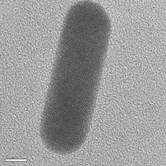
18 Transmission Electron Microscopy 0.1 μm 0.1 μm TEM images of Au-SWNTs composite acquired at 100 kev.

19 10 nm TEM images of (A) AuNRs-SWNTs composite acquired at 300 kev.
20 52k (A) 40k (B) 50k Intensity (arb. units) 48k 46k 44k Intensity (arb. units) 38k 36k 42k Binding energy (ev) 34k Binding Energy (ev) XPS spectra of Au-SWNT composite in the (A) Ni 2p and (B) Fe 2p regions. ICP - MS
 Emission")
 supernatant solution and (B) blank")
21 (A) (B) Excitation wavelength (nm) Emission wavelength (nm) Emission wavelength (nm) Fluorescence contour plots of (A) supernatant solution and (B) blank water at ph 7.12.


22 Instrumentation Confocal Raman Concept of confocality Raman Instrument
23 Key instrument specifications Argon Ion laser : nm Back scattering geometry Super notch filter
24 Scanning Near-field Optical Microscopy Resolution is limited by wavelength of light used. Near-filed microscopy was first proposed by Synge in Resolutions below the diffraction limit can be obtained when the tip-sample distance is smaller than the aperture diameter. In such a case, the aperture diameter controls the resolution and not the wavelength of light used Phil. Mag., 1928, 6, 356.
25 Intensity (arb. units) k 20k 15k 10k Wavelength (nm) k Wavelength (nm) (ii) (a) (b) (c) 669 2k 1k k G` band (d) Raman Shift (cm -1 ) (e) Raman Shift (cm -1 ) (i) Raman Spectra of (a) Ag-SWNTs composite, (b) Au-SWNTs composite, (c) AuNR-SWNTs composite, (d) pristine SWNTs, (e) Pristine SWNTs treated with trisodium citrate and (f) Au nanorods.
 25k 20k 15k 10k 5k 0 2000 4000 6000 8000 Raman")
26 Raman Spectral imaging Intensity (arb. units) 25k 20k 15k 10k 5k Raman Shift (cm -1 ) 7 μm
27 Varying excitation sources a b Wavelength (nm) Excitation : 532 nm a b Excitation : 633 nm c c Raman Shift (cm -1 ) Raman Shift (cm -1 ) Raman Spectra acquired with (A) 532 nm Nd-YAG and (B) 633 nm He-Ne as excitation sources. Traces (a), (b) and (c) correspond to Ag-SWNTs composite, Au-SWNTs composite and AuNR-SWNTs composite, respectively.
")
 and (D) are their three")
28 5 μm (A) SNOM images of Au-SWNT composite along with the (C) topography. (B) and (D) are their three dimensional representations.

 light")
29 (A) (B) Transmission SNOM images of pristine SWNT based on (A) topography and (B) light intensity.
30 Supporting experiments Intensity (arb.units) (A) C CTAB = 10-6 M C CTAB = 10-5 M C CTAB = 10-4 M C CTAB = 10-3 M C CTAB = 10-2 M C CTAB = 10-1 M (B) Raman Shift (cm -1 ) 100 nm (A) Raman spectra of Ag-SWNT composite measured as a function of CTAB concentration. (B) TEM image of Au-CTAB-SWNT at C CTAB = 10-4 M
31 90 (A) Au 4f 7/2 105 (B) Ag 3d 5/2 Intensity (arb. units) Au 4f 5/2 Intensity (arb. units) Ag 3d 3/ Binding energy (ev) Binding Energy (ev) XPS spectra of (A) Au-SWNT and (B) Ag-SWNT composites in the Au 4f and Ag 3d regions, respectively
32 Intensity (arb. units) 25k 20k 15k 10k 5k (A) Intensity (arb. units) 20k 10k (B) C SWNT = 1.7 mg/ml C SWNT /2 C SWNT /3 C SWNT /4 C SWNT /5 C SWNT / Raman Shift (cm -1 ) Raman Shift (cm -1 ) Raman spectra of Ag-SWNT composite, measured as a function of (A) concentration of Ag nanoparticles, (B) SWNT concentration.
33 (n,m) indexing d t RBM 3 C 1 C constants 2, where C1 and C2 are d a c c t n 2 nm m 2 (n,m) RBM d t (nm) (cm -1,Theoretical) (10,10) (18,0) (13,7) (17,0) (11,9) (12,8) m E 11 s s E / 23 E32
34 What we know so far Visible fluorescence from SWNTs is demonstrated. Raman spectral mapping is done to ascertain the origin of fluorescence. SNOM of SWNT structures is done using this fluorescence.
35 Origin of visible fluorescence Near-infrared fluorescence in isolated SWNT is known. This is not observed in bundles and metallic SWNTs. Metallic SWNTs offer non-radiative decay channels. So what happens to the metallic SWNTs present in the composite?
36 Separation protocol SWNT + isopropyl amine + THF Ultrasonicate, 1h SWNT dispersion 40,000 g, 16 0 C, 12h Centrifugate Residue J. Am. Chem. Soc., 2005, 127, Alkyl amines stabilize metallic SWNT
37 Estimating metallic content Point Contact Current Imaging AFM (PCI-AFM) Mica/Insulating substrate Thermo evaporation of gold Quartz microbalance To pump Gold Resistive wires
 Photograph of the")
 representative AFM image of")
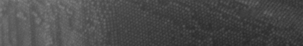
38 (A) Measurement geometry (B) (C) Nanotube Mica/insulating substrate (A) Photograph of the scanning head, (B) schematic of the PCI-AFM measurement and (C) representative AFM image of pristine SWNTs
 (A) PCI-AFM images of pure mswnt with (B) I-V curves and (C) plot of conductance versus bias voltage.")
39 (A) Current (na) (B) (C) Bias Voltage (V) Electrode is 200 nm away from the image-edge 100 nm Conductivity (na/v) Bias Voltage (V) (A) PCI-AFM images of pure mswnt with (B) I-V curves and (C) plot of conductance versus bias voltage.
40 (A) 40 (B) Current (na) Bias Voltage (V) Current (na) nm 200 nm Bias Voltage (V) (C) 400 (D) Current (na) Current (na) nm Bias Voltage (V) nm Bias Voltage (V)
41 (E) 100 nm (F) 1 Current (na) Bias Voltage (V) Current (na) Bias Voltage (V) 1 G1 G b 4 1a 2a 3a 4a 2b 5a 3b 6a 4b 5b G4 6b G2 (G) 200 nm
 (A) PCI-AFM image of Au-mSWNT with (B) the corresponding I-V curves and (C) Plot of conductance versus bias voltage. 1 Au nanoparticle Carbon nanotubes")
42 10 (B) 5 (A) Electrode is 420 nm away from the edge nm 2 Conductance (na/v) Current (na) Bias Voltage (V) (C) Bias Voltage (V) (A) PCI-AFM image of Au-mSWNT with (B) the corresponding I-V curves and (C) Plot of conductance versus bias voltage. 1 Au nanoparticle Carbon nanotubes
43 80 60 Bias Voltage (V) Pure mswnt Au-mSWNT Conductance (na/v) Conductance (na/v) Bias Voltage (V) Comparison of conductance versus bias voltage for pure mswnt and AumSWNT composite
44 G-band line shapes of metallic and semiconducting SWNT Changes observed in G-band for metallic (left) and pristine (right) SWNT Science, 2003, 301, 345.
45 Confocal Raman investigations 700 Intensity (arb. units) A s /A m = 65.0 A s /A m = 0.14 Extraction efficiency A s /(A s + A m )* 100 = 88% Raman Shift (cm -1 ) Raman spectra in RBM and G-band regions of pristine SWNT (black) and extracted mswnt (red).
46 Pure mswnt FWHM = 48 cm -1 Au- mswnt FWHM = 22 cm Raman Shift (cm -1 ) Raman Shift (cm -1 ) Comparison of G-band of pure mswnt and Au-mSWNT
47 Conclusions Metallicity of SWNT is destroyed by interaction with nanoparticles. PCI-AFM and confocal Raman confirm this M-S transition. mswnt fluoresce when their metallicity is destroyed. M-S transition has far reaching implication in nanoelectronics and design of nanodevices. C. Subramaniam et al. Phys. Rev. Lett. (2007) C. Subramaniam and T. Pradeep Patent applications 2005, 2006, 2007
48 Application of fluorescence in gas sensing and separation

49 Fuel Cells : Methanol fuel cells, metal- hydride fuel cells, Gas storage materials Carbon nanotubes 1600 m 2 /g 1 5% of publications relate to gas storage 1 1 Acc. Chem. Res., 2007, DOI : /ar700013c


50 Specific adsorption sites Interstitial site Endohedral Site Groove site External site Loadings from 0.08 wt% to 12 wt % have been reported
51 Experimental setup To rotary pump To Hg manometer To gas source To rotary pump To Raman spectrometer Fibre optic pin-hole detection Super-notch filter Open/close valve Sample compartment Sample
52 Intensity (arb. units) 6k 5k 4k 3k 2k Raman Shift (cm -1 ) 10 torr 20 torr 30 torr 40 torr 60 torr 100 torr 140 torr 175 torr 200 torr 220 torr 250 torr 275 torr 320 torr 350 torr Au-SWNTs exposed to He gas at various partial pressures.
53 4.0k 0 torr Intensity 3.5k 3.0k 2.5k 2.0k 550 torr 1.5k Raman Shift (cm -1 ) Au-SWNTs exposed to H 2 gas at various partial pressures.
54 Fluorescence intensity (a.u.) % Groove sites Endohedral & interstitial sites 32% External sites, 9% Pressure of hydrogen (torr)
55 5.0k 4.5k 0 torr 500 torr Intenisty (arb. units) 4.0k 3.5k 3.0k 2.5k 2.0k 1.5k Raman Shift (cm -1 ) Au-SWNTs exposed to N 2 gas at various partial pressures.
56 Gas separation possibility Intensity (arb. units) 3.0k 2.5k 2.0k 1.5k 1.0k In vacuum 100 torr H torr H torr N torr removed In vacuum Raman Shift (cm -1 )
57 Intensity (arb. units) In vacuum 100 torr N torr N torr H torr gas removed In vacuum Raman Shift (cm -1 )
58 Intensity (arb. units) 4.5k 4.0k 3.5k 3.0k 2.5k 2.0k 1.5k 1.0k Raman Shift (cm -1 ) Vacuum 10 torr 20 torr 30 torr 40 torr 50 torr 75 torr 100 torr 125 torr 150 torr 175 torr 200 torr 225 torr 250 torr 275 torr 300 torr 325 torr 350 torr 375 torr 400 torr 425 torr 450 torr 475 torr Methane on Au-SWNTs
59 Intensity (arb. units) 3.5k 3.0k 2.5k 2.0k 1.5k 1.0k Vacuum 10 torr 20 torr 30 torr 40 torr 50 torr 60 torr 75 torr 100 torr Raman Shift (cm -1 ) n-hexane on Au-SWNTs
60 Intensity (arb. units) Raman Shift (cm -1 ) Cyclohexane on Au-SWNTs Vacuum 10 torr 20 torr 40 torr 50 torr 60 torr Vacuum


61


62 5 1 1 II I
63 5 I Current(nA) Au-mSWNT with N Bias Voltage (V)
64 80 I Conductance (na/v) Au-mSWNT with N Bias Voltage (V)
65 20 I 10 Current (na) 0-10 Au-mSWNT with H Bias Voltage (V)
66 50 40 I Au-mSWNT with H 2 Conductance (na/v) Bias Voltage (V)
67 50 Conductance (na/v) Au-mSWNT + Nitrogen Au-mSWNT + Hydrogen Bias voltage (V) Plot of conductance versus bias voltage constructed at various point of Figure 1A, under an atmosphere of nitrogen (red traces) and hydrogen (black traces).
68 (B) Intensity (a.u.) (c) (d) (b) (a) (b) (d) (c) (a) 1800 Raman Shift (cm -1 ) Raman spectra of (a) purified mswnts, (b) Au-mSWNT composite, (c) Au-mSWNT upon exposure to 500 torr H 2 and (d) Au-mSWNT composite after pumping out H 2 exposed in (c). Spectra (a) to (d) are recorded at the same point on the composite sample.
69 Conclusions and future directions Gas adsorption inside SWNT was studied using visible fluorescence from Au-SWNTs composite Behavior was similar in case of Ag-SWNT and AuNR-SWNT composites. In-situ gas storage detection Observation of different adsorption sites Gas separation Understanding gas storage inside SWNTs Probing electronic structure variation upon gas adsorption Possibilities of isomer separation C. Subramaniam and T. Pradeep Patent application 2007


70 Thank you all IIT Madras
SUPPLEMENTARY INFORMATION
 SUPPLEMENTARY INFORMATION doi: 1.138/nphoton.211.25 Efficient Photovoltage Multiplication in Carbon Nanotubes Leijing Yang 1,2,3+, Sheng Wang 1,2+, Qingsheng Zeng, 1,2, Zhiyong Zhang 1,2, Tian Pei 1,2,
Microscopic Structures
 Microscopic Structures Image Analysis Metal, 3D Image (Red-Green) The microscopic methods range from dark field / bright field microscopy through polarisation- and inverse microscopy to techniques like
Jian-Wei Liu, Jing Zheng, Jin-Long Wang, Jie Xu, Hui-Hui Li, Shu-Hong Yu*
 Supporting Information Ultrathin 18 O 49 Nanowire Assemblies for Electrochromic Devices Jian-ei Liu, Jing Zheng, Jin-Long ang, Jie Xu, Hui-Hui Li, Shu-Hong Yu* Experimental Section Synthesis and Assembly
Integrated into Nanowire Waveguides
 Supporting Information Widely Tunable Distributed Bragg Reflectors Integrated into Nanowire Waveguides Anthony Fu, 1,3 Hanwei Gao, 1,3,4 Petar Petrov, 1, Peidong Yang 1,2,3* 1 Department of Chemistry,
photolithographic techniques (1). Molybdenum electrodes (50 nm thick) are deposited by
. Molybdenum electrodes (50 nm thick) are deposited by") Supporting online material Materials and Methods Single-walled carbon nanotube (SWNT) devices are fabricated using standard photolithographic techniques (1). Molybdenum electrodes (50 nm thick) are deposited
Supporting online material Materials and Methods Single-walled carbon nanotube (SWNT) devices are fabricated using standard photolithographic techniques (1). Molybdenum electrodes (50 nm thick) are deposited
Supporting Information. Superluminescence from an optically pumped. molecular tunneling junction by injection of plasmon
 Supporting Information for Superluminescence from an optically pumped molecular tunneling junction by injection of plasmon induced hot electrons Kai Braun, Xiao Wang, Andreas M. Kern, Hilmar Adler, Heiko
*Corresponding author.
 Supporting Information for: Ligand-Free, Quantum-Confined Cs 2 SnI 6 Perovskite Nanocrystals Dmitriy S. Dolzhnikov, Chen Wang, Yadong Xu, Mercouri G. Kanatzidis, and Emily A. Weiss * Department of Chemistry,
Approachable Raman Solutions The Shortest Path from Problem to Answer
 Approachable Raman Solutions The Shortest Path from Problem to Answer Michael S. Bradley The world leader in serving science Thermo Scientific Raman Spectroscopy: Discover. Solve. Assure. Raman Spectroscopy
Monitoring of Galvanic Replacement Reaction. between Silver Nanowires and HAuCl 4 by In-Situ. Transmission X-Ray Microscopy
 Supporting Information Monitoring of Galvanic Replacement Reaction between Silver Nanowires and HAuCl 4 by In-Situ Transmission X-Ray Microscopy Yugang Sun *, and Yuxin Wang Center for Nanoscale Materials
Spectral phase shaping for high resolution CARS spectroscopy around 3000 cm 1
 Spectral phase shaping for high resolution CARS spectroscopy around 3 cm A.C.W. van Rhijn, S. Postma, J.P. Korterik, J.L. Herek, and H.L. Offerhaus Mesa + Research Institute for Nanotechnology, University
Nanonics Systems are the Only SPMs that Allow for On-line Integration with Standard MicroRaman Geometries
 Nanonics Systems are the Only SPMs that Allow for On-line Integration with Standard MicroRaman Geometries 2002 Photonics Circle of Excellence Award PLC Ltd, England, a premier provider of Raman microspectral
Beams and Scanning Probe Microscopy
 IFN-CNR, Sezione di Trento Istituto Trentino di Cultura of Trento Department of Physics University of Trento Towards the joint use of X-ray Beams and Scanning Probe Microscopy Silvia Larcheri SILS 2005
Author(s) Issue Date Text Version author. DOI / /18/9/095501
 Issue Date Text Version author. DOI / /18/9/095501") Title Author(s) Citation Refinement of Conditions of Point-Contact Current Imaging Atomic Force Microscopy for Molecular-Scale Conduction Measurements Yajima, Takashi; Tanaka, Hirofumi; Matsumoto, Takuya;
Title Author(s) Citation Refinement of Conditions of Point-Contact Current Imaging Atomic Force Microscopy for Molecular-Scale Conduction Measurements Yajima, Takashi; Tanaka, Hirofumi; Matsumoto, Takuya;
Chemical Imaging. Whiskbroom Imaging. Staring Imaging. Pushbroom Imaging. Whiskbroom. Staring. Pushbroom
 Chemical Imaging Whiskbroom Chemical Imaging (CI) combines different technologies like optical microscopy, digital imaging and molecular spectroscopy in combination with multivariate data analysis methods.
Structural, optical, and electrical properties of phasecontrolled cesium lead iodide nanowires
 Electronic Supplementary Material Structural, optical, and electrical properties of phasecontrolled cesium lead iodide nanowires Minliang Lai 1, Qiao Kong 1, Connor G. Bischak 1, Yi Yu 1,2, Letian Dou
Supporting Information 1. Experimental
 Supporting Information 1. Experimental The position markers were fabricated by electron-beam lithography. To improve the nanoparticle distribution when depositing aqueous Ag nanoparticles onto the window,
You won t be able to measure the incident power precisely. The readout of the power would be lower than the real incident power.
 1. a) Given the transfer function of a detector (below), label and describe these terms: i. dynamic range ii. linear dynamic range iii. sensitivity iv. responsivity b) Imagine you are using an optical
Yuta Sato, Kazu Suenaga, Shingo Okubo, Toshiya Okazaki, and Sumio Iijima
 The Structures of D 5d -C 80 and I h -Er 3 N@C 80 Fullerenes and their Rotation inside Carbon Nanotubes demonstrated by Aberration-Corrected Electron Microscopy Yuta Sato, Kazu Suenaga, Shingo Okubo, Toshiya
Electrical and Optical Tunability in All-Inorganic Halide. Perovskite Alloy Nanowires
 Supporting Information for: Electrical and Optical Tunability in All-Inorganic Halide Perovskite Alloy Nanowires Teng Lei, 1 Minliang Lai, 1 Qiao Kong, 1 Dylan Lu, 1 Woochul Lee, 2 Letian Dou, 3 Vincent
Ultrafast Surface-Enhanced Raman Probing of the Role of Hot Electrons in Plasmon-Driven Chemistry. Supporting Information
 Methods Ultrafast Surface-Enhanced Raman Probing of the Role of Hot Electrons in Plasmon-Driven Chemistry Sample preparation Supporting Information Nathaniel C. Brandt, Emily L. Keller, and Renee R. Frontiera
Highly efficient SERS nanowire/ag composites
 Highly efficient SERS nanowire/ag composites S.M. Prokes, O.J. Glembocki and R.W. Rendell Electronics Science and Technology Division Introduction: Optically based sensing provides advantages over electronic
Improving the Collection Efficiency of Raman Scattering
 PERFORMANCE Unparalleled signal-to-noise ratio with diffraction-limited spectral and imaging resolution Deep-cooled CCD with excelon sensor technology Aberration-free optical design for uniform high resolution
Supporting Information. Single-Nanowire Electrochemical Probe Detection for Internally Optimized Mechanism of
 Supporting Information Single-Nanowire Electrochemical Probe Detection for Internally Optimized Mechanism of Porous Graphene in Electrochemical Devices Ping Hu, Mengyu Yan, Xuanpeng Wang, Chunhua Han,*
NSOM (SNOM) Overview
 Overview") NSOM (SNOM) Overview The limits of far field imaging In the early 1870s, Ernst Abbe formulated a rigorous criterion for being able to resolve two objects in a light microscope: d > ë / (2sinè) where d
NSOM (SNOM) Overview The limits of far field imaging In the early 1870s, Ernst Abbe formulated a rigorous criterion for being able to resolve two objects in a light microscope: d > ë / (2sinè) where d
Ultraviolet Visible Infrared Instrumentation
 Ultraviolet Visible Infrared Instrumentation Focus our attention on measurements in the UV-vis region of the EM spectrum Good instrumentation available Very widely used techniques Longstanding and proven
Supporting Information. High-Resolution Organic Light Emitting Diodes Patterned via Contact Printing
 Supporting Information High-Resolution Organic Light Emitting Diodes Patterned via Contact Printing Jinhai Li, Lisong Xu, Ching W. Tang and Alexander A. Shestopalov* Department of Chemical Engineering,
Method for Controlling Electrical Properties of Single-Layer. Graphene Nanoribbons via Adsorbed Planar Molecular. Nanoparticles
 Supplementary Information Method for Controlling Electrical Properties of Single-Layer Graphene Nanoribbons via Adsorbed Planar Molecular Nanoparticles Hirofumi Tanaka, 1,2,* Ryo Arima, 1 Minoru Fukumori,
:... resolution is about 1.4 μm, assumed an excitation wavelength of 633 nm and a numerical aperture of 0.65 at 633 nm.
 PAGE 30 & 2008 2007 PRODUCT CATALOG Confocal Microscopy - CFM fundamentals :... Over the years, confocal microscopy has become the method of choice for obtaining clear, three-dimensional optical images
Supporting Materials for. A Novel Color Modulation Analysis Strategy. through Tunable Multiband Laser for. Nanoparticle Identification and Evaluation
 Supporting Materials for A Novel Color Modulation Analysis Strategy through Tunable Multiband Laser for Nanoparticle Identification and Evaluation Xuan Cao,, Gang Lei, Jingjing Feng, Qi Pan, Xiaodong Wen,
Chemistry 524--"Hour Exam"--Keiderling Mar. 19, pm SES
 Chemistry 524--"Hour Exam"--Keiderling Mar. 19, 2013 -- 2-4 pm -- 170 SES Please answer all questions in the answer book provided. Calculators, rulers, pens and pencils permitted. No open books allowed.
Supplementary Materials for
 advances.sciencemag.org/cgi/content/full/4/2/e1700324/dc1 Supplementary Materials for Photocarrier generation from interlayer charge-transfer transitions in WS2-graphene heterostructures Long Yuan, Ting-Fung
Study of shear force as a distance regulation mechanism for scanning near-field optical microscopy
 Study of shear force as a distance regulation mechanism for scanning near-field optical microscopy C. Durkan a) and I. V. Shvets Department of Physics, Trinity College Dublin, Ireland Received 31 May 1995;
Raman Spectroscopy and Transmission Electron Microscopy of Si x Ge 1-x -Ge-Si Core-Double-Shell Nanowires
 Raman Spectroscopy and Transmission Electron Microscopy of Si x Ge 1-x -Ge-Si Core-Double-Shell Nanowires Paola Perez Mentor: Feng Wen PI: Emanuel Tutuc Background One-dimensional semiconducting nanowires
Advanced Research Raman System Raman Spectroscopy Systems
 T600 Advanced Research Raman System Raman Spectroscopy Systems T600 Advanced Research Raman System T600 Triple stage Raman Spectrometer: The only solution for unprecedented stability and performance! Robust
Multi-Functions of Net Surface Charge in the Reaction. on a Single Nanoparticle
 Multi-Functions of Net Surface Charge in the Reaction on a Single Nanoparticle Shaobo Xi 1 and Xiaochun Zhou* 1,2 1 Division of Advanced Nanomaterials, 2 Key Laboratory of Nanodevices and Applications,
attocfm I for Surface Quality Inspection NANOSCOPY APPLICATION NOTE M01 RELATED PRODUCTS G
 APPLICATION NOTE M01 attocfm I for Surface Quality Inspection Confocal microscopes work by scanning a tiny light spot on a sample and by measuring the scattered light in the illuminated volume. First,
Nanoscale Systems for Opto-Electronics
 Nanoscale Systems for Opto-Electronics 675 PL intensity [arb. units] 700 Wavelength [nm] 650 625 600 5µm 1.80 1.85 1.90 1.95 Energy [ev] 2.00 2.05 1 Nanoscale Systems for Opto-Electronics Lecture 5 Interaction
Ppm detection of alcohol vapors via metal organic framework functionalized surface plasmon resonance sensors
 Supporting Information Ppm detection of alcohol vapors via metal organic framework functionalized surface plasmon resonance sensors Wouter Vandezande a, Filip Delport c, Kris P.F. Janssen b, Rob Ameloot
attosnom I: Topography and Force Images NANOSCOPY APPLICATION NOTE M06 RELATED PRODUCTS G
 APPLICATION NOTE M06 attosnom I: Topography and Force Images Scanning near-field optical microscopy is the outstanding technique to simultaneously measure the topography and the optical contrast of a sample.
Generation of ultra-fast laser pulses using nanotube mode-lockers
 phys. stat. sol. (b) 243, No. 13, 3551 3555 (2006) / DOI 10.1002/pssb.200669151 Generation of ultra-fast laser pulses using nanotube mode-lockers A. G. Rozhin 1, V. Scardaci 1, F. Wang 1, F. Hennrich 2,
Supplementary Figure S1 X-ray diffraction pattern of the Ag nanowires shown in Fig. 1a dispersed in their original solution. The wavelength of the
 Supplementary Figure S1 X-ray diffraction pattern of the Ag nanowires shown in Fig. 1a dispersed in their original solution. The wavelength of the x-ray beam was 0.1771 Å. The saturated broad peak and
Individually color-coded plasmonic nanoparticles for RGB analysis
 Electronic Supplementary Information Individually color-coded plasmonic nanoparticles for RGB analysis Yue Liu a, Jian Ling b, and Cheng Zhi Huang *a,c a Education Ministry Key Laboratory on Luminescence
Supporting Information for DNA Origami and G- Quadruplex Hybrid Complexes Induce Size- Control of Single- Walled Carbon
 Supporting Information for DNA Origami and G- Quadruplex Hybrid Complexes Induce Size- Control of Single- Walled Carbon Nanotubes via Biological Activation Hiroshi Atsumi 1,2 and Angela M. Belcher 1,2,3*
Nanofluidic Diodes based on Nanotube Heterojunctions
 Supporting Information Nanofluidic Diodes based on Nanotube Heterojunctions Ruoxue Yan, Wenjie Liang, Rong Fan, Peidong Yang 1 Department of Chemistry, University of California, Berkeley, CA 94720, USA
SUPPLEMENTARY INFORMATION
 SUPPLEMENTARY INFORMATION Supplementary Information Real-space imaging of transient carrier dynamics by nanoscale pump-probe microscopy Yasuhiko Terada, Shoji Yoshida, Osamu Takeuchi, and Hidemi Shigekawa*
SYNTHESIS AND CHARACTERIZATION OF II-IV GROUP AND SILICON RELATED NANOMATERIALS
 SYNTHESIS AND CHARACTERIZATION OF II-IV GROUP AND SILICON RELATED NANOMATERIALS ISMATHULLAKHAN SHAFIQ MASTER OF PHILOSOPHY CITY UNIVERSITY OF HONG KONG FEBRUARY 2008 CITY UNIVERSITY OF HONG KONG 香港城市大學
Supporting Information. Epitaxially Aligned Cuprous Oxide Nanowires for All-Oxide, Single-Wire Solar Cells
 Supporting Information Epitaxially Aligned Cuprous Oxide Nanowires for All-Oxide, Single-Wire Solar Cells Sarah Brittman, 1,2 Youngdong Yoo, 1 Neil P. Dasgupta, 1,3 Si-in Kim, 4 Bongsoo Kim, 4 and Peidong
Morphological Effect of Gold Nanoparticle on the. Adsorption of Bovine Serum Albumin
 Electronic Supplementary Material (ESI) for Physical Chemistry Chemical Physics. This journal is the Owner Societies 014 Supporting Information Morphological Effect of Gold Nanoparticle on the Adsorption
SUPPLEMENTAL MATERIAL
 SUPPLEMENTAL MATERIAL 1 - Folios and areas of analysis Figure S1.1. Folio 4, areas of analysis for microxrf ( ), FORS ( ), micro-samples for Raman and FTIR ( ) and Raman in-situ ( ). Figure S1.2. Folio
S.Vidhya by, Published 4 Feb 2014
 A Wearable And Highly Sensitive Pressure Sensor With Ultrathin Gold Nanowires Shu Gong1,2, Willem Schwalb3, Yongwei Wang1,2, Yi Chen1, Yue Tang1,2, Jye Si1, Bijan Shirinzadeh3 & Wenlong Cheng1,2 1 Department
Applications of Steady-state Multichannel Spectroscopy in the Visible and NIR Spectral Region
 Feature Article JY Division I nformation Optical Spectroscopy Applications of Steady-state Multichannel Spectroscopy in the Visible and NIR Spectral Region Raymond Pini, Salvatore Atzeni Abstract Multichannel
Transparent p-type SnO Nanowires with Unprecedented Hole Mobility among Oxide Semiconductors
 Supplementary Information Transparent p-type SnO Nanowires with Unprecedented Hole Mobility among Oxide Semiconductors J. A. Caraveo-Frescas and H. N. Alshareef* Materials Science and Engineering, King
SUPPLEMENTARY INFORMATION
 Figure S. Experimental set-up www.nature.com/nature Figure S2. Dependence of ESR frequencies (GHz) on a magnetic field (G) applied in different directions with respect to NV axis ( θ 2π). The angle with
Photonics and Fiber Optics
 1 UNIT V Photonics and Fiber Optics Part-A 1. What is laser? LASER is the acronym for Light Amplification by Stimulated Emission of Radiation. The absorption and emission of light by materials has been
Nd: YAG Laser Energy Levels 4 level laser Optical transitions from Ground to many upper levels Strong absorber in the yellow range None radiative to
 Nd: YAG Lasers Dope Neodynmium (Nd) into material (~1%) Most common Yttrium Aluminum Garnet - YAG: Y 3 Al 5 O 12 Hard brittle but good heat flow for cooling Next common is Yttrium Lithium Fluoride: YLF
COMPONENTS OF OPTICAL INSTRUMENTS. Chapter 7 UV, Visible and IR Instruments
 COMPONENTS OF OPTICAL INSTRUMENTS Chapter 7 UV, Visible and IR Instruments 1 Topics A. GENERAL DESIGNS B. SOURCES C. WAVELENGTH SELECTORS D. SAMPLE CONTAINERS E. RADIATION TRANSDUCERS F. SIGNAL PROCESSORS
COMPONENTS OF OPTICAL INSTRUMENTS. Topics
 COMPONENTS OF OPTICAL INSTRUMENTS Chapter 7 UV, Visible and IR Instruments Topics A. GENERAL DESIGNS B. SOURCES C. WAVELENGTH SELECTORS D. SAMPLE CONTAINERS E. RADIATION TRANSDUCERS F. SIGNAL PROCESSORS
SUPPLEMENTARY INFORMATION
 In the format provided by the authors and unedited. Photon-triggered nanowire transistors Jungkil Kim, Hoo-Cheol Lee, Kyoung-Ho Kim, Min-Soo Hwang, Jin-Sung Park, Jung Min Lee, Jae-Pil So, Jae-Hyuck Choi,
Single Nanoparticle Plasmonic Electro-Optic Modulator Based on MoS 2 Monolayers
 Single Nanoparticle Plasmonic Electro-Optic Modulator Based on MoS 2 Monolayers Bowen Li,, Shuai Zu,, Jiadong Zhou, Qiao Jiang, Bowen Du, Hangyong Shan, Yang Luo, Zheng Liu, Xing Zhu, and Zheyu Fang,*
Supporting Information
 Supporting Information Eaton et al. 10.1073/pnas.1600789113 Additional Characterization and Simulation of CsPbX 3 Nanowires and Plates Atomic Force Microscopy Measurements. Atomic force microscopy (AFM)
7 CHAPTER 7: REFRACTIVE INDEX MEASUREMENTS WITH COMMON PATH PHASE SENSITIVE FDOCT SETUP
 7 CHAPTER 7: REFRACTIVE INDEX MEASUREMENTS WITH COMMON PATH PHASE SENSITIVE FDOCT SETUP Abstract: In this chapter we describe the use of a common path phase sensitive FDOCT set up. The phase measurements
Gigahertz Ambipolar Frequency Multiplier Based on Cvd Graphene
 Gigahertz Ambipolar Frequency Multiplier Based on Cvd Graphene The MIT Faculty has made this article openly available. Please share how this access benefits you. Your story matters. Citation As Published
Cavity QED with quantum dots in semiconductor microcavities
 Cavity QED with quantum dots in semiconductor microcavities M. T. Rakher*, S. Strauf, Y. Choi, N.G. Stolz, K.J. Hennessey, H. Kim, A. Badolato, L.A. Coldren, E.L. Hu, P.M. Petroff, D. Bouwmeester University
Hierarchical CoNiSe2 nano-architecture as a highperformance electrocatalyst for water splitting
 Nano Res. Electronic Supplementary Material Hierarchical CoNiSe2 nano-architecture as a highperformance electrocatalyst for water splitting Tao Chen and Yiwei Tan ( ) State Key Laboratory of Materials-Oriented
Photoresist erosion studied in an inductively coupled plasma reactor employing CHF 3
 Photoresist erosion studied in an inductively coupled plasma reactor employing CHF 3 M. F. Doemling, N. R. Rueger, and G. S. Oehrlein a) Department of Physics, University at Albany, State University of
Directional Growth of Ultra-long CsPbBr 3 Perovskite. Nanowires for High Performance Photodetectors
 Supporting information Directional Growth of Ultra-long CsPbBr 3 Perovskite Nanowires for High Performance Photodetectors Muhammad Shoaib, Xuehong Zhang, Xiaoxia Wang, Hong Zhou, Tao Xu, Xiao Wang, Xuelu
Fabrication of Probes for High Resolution Optical Microscopy
 Fabrication of Probes for High Resolution Optical Microscopy Physics 564 Applied Optics Professor Andrès La Rosa David Logan May 27, 2010 Abstract Near Field Scanning Optical Microscopy (NSOM) is a technique
Nd:YSO resonator array Transmission spectrum (a. u.) Supplementary Figure 1. An array of nano-beam resonators fabricated in Nd:YSO.
 Supplementary Figure 1. An array of nano-beam resonators fabricated in Nd:YSO.") a Nd:YSO resonator array µm Transmission spectrum (a. u.) b 4 F3/2-4I9/2 25 2 5 5 875 88 λ(nm) 885 Supplementary Figure. An array of nano-beam resonators fabricated in Nd:YSO. (a) Scanning electron microscope
a Nd:YSO resonator array µm Transmission spectrum (a. u.) b 4 F3/2-4I9/2 25 2 5 5 875 88 λ(nm) 885 Supplementary Figure. An array of nano-beam resonators fabricated in Nd:YSO. (a) Scanning electron microscope
Georgia O'Keeffe. THE Alfred Stieglitz COLLECTION OBJECT RESEARCH Palladium print Alfred Stieglitz Collection. AIC accession number: 1949.
 Alfred Stieglitz (American, 1864 1946) Georgia O'Keeffe 1918 Palladium print Alfred Stieglitz Collection AIC accession number: 1949.745A Stieglitz Estate number: OK 19E Inscriptions: Unmarked recto; inscribed
Electronic Supplementary Information
 Electronic Supplementary Information Differential Interference Contrast Microscopy Imaging of Micrometer-Long Plasmonic Nanowires Ji Won Ha, Kuangcai Chen, and Ning Fang * Ames Laboratory, U.S. Department
High-Resolution Bubble Printing of Quantum Dots
 SUPPORTING INFORMATION High-Resolution Bubble Printing of Quantum Dots Bharath Bangalore Rajeeva 1, Linhan Lin 1, Evan P. Perillo 2, Xiaolei Peng 1, William W. Yu 3, Andrew K. Dunn 2, Yuebing Zheng 1,*
X-Ray Spectroscopy with a CCD Detector. Application Note
 X-Ray Spectroscopy with a CCD Detector In addition to providing X-ray imaging solutions, including CCD-based cameras that image X-rays using either direct detection (0.5-20 kev) or indirectly using a scintillation
Fast Raman Spectral Imaging Using Chirped Femtosecond Lasers
 Fast Raman Spectral Imaging Using Chirped Femtosecond Lasers Dan Fu 1, Gary Holtom 1, Christian Freudiger 1, Xu Zhang 2, Xiaoliang Sunney Xie 1 1. Department of Chemistry and Chemical Biology, Harvard
Optimization of supercontinuum generation in photonic crystal fibers for pulse compression
 Optimization of supercontinuum generation in photonic crystal fibers for pulse compression Noah Chang Herbert Winful,Ted Norris Center for Ultrafast Optical Science University of Michigan What is Photonic
plasmonic nanoblock pair
 Nanostructured potential of optical trapping using a plasmonic nanoblock pair Yoshito Tanaka, Shogo Kaneda and Keiji Sasaki* Research Institute for Electronic Science, Hokkaido University, Sapporo 1-2,
MoS 2 nanosheet phototransistors with thicknessmodulated
 Supporting Information MoS 2 nanosheet phototransistors with thicknessmodulated optical energy gap Hee Sung Lee, Sung-Wook Min, Youn-Gyung Chang, Park Min Kyu, Taewook Nam, # Hyungjun Kim, # Jae Hoon Kim,
Scanning Tunneling Microscopy
 Scanning Tunneling Microscopy The wavelike properties of electrons allows them to tunnel beyond the regions of a solid into a region of space forbidden for them to exist in. In this region they can be
PH880 Topics in Physics
 PH880 Topics in Physics Modern Optical Imaging (Fall 2010) Overview of week 12 Monday: FRET Wednesday: NSOM Förster resonance energy transfer (FRET) Fluorescence emission i FRET Donor Acceptor wikipedia
Nanovie. Scanning Tunnelling Microscope
 Nanovie Scanning Tunnelling Microscope Nanovie STM Always at Hand Nanovie STM Lepto for Research Nanovie STM Educa for Education Nanovie Auto Tip Maker Nanovie STM Lepto Portable 3D nanoscale microscope
Nano-structured superconducting single-photon detector
 Nano-structured superconducting single-photon detector G. Gol'tsman *a, A. Korneev a,v. Izbenko a, K. Smirnov a, P. Kouminov a, B. Voronov a, A. Verevkin b, J. Zhang b, A. Pearlman b, W. Slysz b, and R.
Glass and Bioglass Nanopowders by Flame Synthesis
 Supplementary Information Glass and Bioglass Nanopowders by Flame Synthesis Tobias J. Brunner, Robert N. Grass, Wendelin J. Stark* Institute for Chemical and Bioengineering, Department of Chemistry and
Microscopy. Matti Hotokka Department of Physical Chemistry Åbo Akademi University
 Microscopy Matti Hotokka Department of Physical Chemistry Åbo Akademi University What s coming Anatomy of a microscope Modes of illumination Practicalities Special applications Basic microscope Ocular
Enable Highly-Stable Plasma Operations at High Pressures with the Right RPS Solution
 Enable Highly-Stable Plasma Operations at High Pressures with the Right RPS Solution Created by Advanced Energy Industries, Inc., Fort Collins, CO Abstract Conventional applications for remote plasma sources
S200 Course LECTURE 1 TEM
 S200 Course LECTURE 1 TEM Development of Electron Microscopy 1897 Discovery of the electron (J.J. Thompson) 1924 Particle and wave theory (L. de Broglie) 1926 Electromagnetic Lens (H. Busch) 1932 Construction
NOVEL APPLICATIONS OF CONFOCAL MICROSCOPY TECHNIQUES IN COATINGS RESEARCH
 ARKEMA COATING RESINS NOVEL APPLICATIONS OF CONFOCAL MICROSCOPY TECHNIQUES IN COATINGS RESEARCH DOUG MALL FOR DR. WENJUN WU 9/20/2018 Wood Coatings & Substrates Conference 2018 OUTLINE Introduction Confocal
TCSPC at Wavelengths from 900 nm to 1700 nm
 TCSPC at Wavelengths from 900 nm to 1700 nm We describe picosecond time-resolved optical signal recording in the spectral range from 900 nm to 1700 nm. The system consists of an id Quantique id220 InGaAs
Supporting Information
 Supporting Information Inverse I-V injection characteristics of ZnO nanoparticle based diodes Paul Mundt 1,2, Stefan Vogel 3, Klaus Bonrad 2,4, Heinz von Seggern 1 * Technische Universität Darmstadt 1
M. Senoner 1), Th. Wirth 1), W. E. S. Unger 1), M. Escher 2), N. Weber 2), D. Funnemann 3) and B. Krömker 3) INTRODUCTION
, Th. Wirth 1), W. E. S. Unger 1), M. Escher 2), N. Weber 2), D. Funnemann 3) and B. Krömker 3) INTRODUCTION") Testing of Lateral Resolution in the Nanometre Range Using the BAM-L002 - Certified Reference Material: Application to ToF-SIMS IV and NanoESCA Instruments M. Senoner 1), Th. Wirth 1), W. E. S. Unger 1),
Testing of Lateral Resolution in the Nanometre Range Using the BAM-L002 - Certified Reference Material: Application to ToF-SIMS IV and NanoESCA Instruments M. Senoner 1), Th. Wirth 1), W. E. S. Unger 1),
Surface Topography and Alignment Effects in UV-Modified Polyimide Films with Micron Size Patterns
 CHINESE JOURNAL OF PHYSICS VOL. 41, NO. 2 APRIL 2003 Surface Topography and Alignment Effects in UV-Modified Polyimide Films with Micron Size Patterns Ru-Pin Pan 1, Hua-Yu Chiu 1,Yea-FengLin 1,andJ.Y.Huang
Fast Laser Raman Microscope RAMAN
 Fast Laser Raman Microscope RAMAN - 11 www.nanophoton.jp Fast Raman Imaging A New Generation of Raman Microscope RAMAN-11 developed by Nanophoton was created by combining confocal laser microscope technology
Single-photon excitation of morphology dependent resonance
 Single-photon excitation of morphology dependent resonance 3.1 Introduction The examination of morphology dependent resonance (MDR) has been of considerable importance to many fields in optical science.
Lithography. 3 rd. lecture: introduction. Prof. Yosi Shacham-Diamand. Fall 2004
 Lithography 3 rd lecture: introduction Prof. Yosi Shacham-Diamand Fall 2004 1 List of content Fundamental principles Characteristics parameters Exposure systems 2 Fundamental principles Aerial Image Exposure
Supporting Information. Absorption of Light in a Single-Nanowire Silicon Solar
 Supporting Information Absorption of Light in a Single-Nanowire Silicon Solar Cell Decorated with an Octahedral Silver Nanocrystal Sarah Brittman, 1,2 Hanwei Gao, 1,2 Erik C. Garnett, 3 and Peidong Yang
Printing Beyond srgb Color Gamut by. Mimicking Silicon Nanostructures in Free-Space
 Supporting Information for: Printing Beyond srgb Color Gamut by Mimicking Silicon Nanostructures in Free-Space Zhaogang Dong 1, Jinfa Ho 1, Ye Feng Yu 2, Yuan Hsing Fu 2, Ramón Paniagua-Dominguez 2, Sihao
Supporting Online Material for
 www.sciencemag.org/cgi/content/full/315/5814/966/dc1 Supporting Online Material for Experimental Realization of Wheeler s Delayed-Choice Gedanken Experiment Vincent Jacques, E Wu, Frédéric Grosshans, François
Confocal Imaging Through Scattering Media with a Volume Holographic Filter
 Confocal Imaging Through Scattering Media with a Volume Holographic Filter Michal Balberg +, George Barbastathis*, Sergio Fantini % and David J. Brady University of Illinois at Urbana-Champaign, Urbana,
Low-energy Electron Diffractive Imaging for Three dimensional Light-element Materials
 Low-energy Electron Diffractive Imaging for Three dimensional Light-element Materials Hitachi Review Vol. 61 (2012), No. 6 269 Osamu Kamimura, Ph. D. Takashi Dobashi OVERVIEW: Hitachi has been developing
PULSED BREAKDOWN CHARACTERISTICS OF HELIUM IN PARTIAL VACUUM IN KHZ RANGE
 PULSED BREAKDOWN CHARACTERISTICS OF HELIUM IN PARTIAL VACUUM IN KHZ RANGE K. Koppisetty ξ, H. Kirkici Auburn University, Auburn, Auburn, AL, USA D. L. Schweickart Air Force Research Laboratory, Wright
Low Voltage Electron Microscope
 LVEM 25 Low Voltage Electron Microscope fast compact powerful Delong America FAST, COMPACT AND POWERFUL The LVEM 25 offers a high-contrast, high-throughput, and compact solution with nanometer resolutions.
Nanodrawing of Aligned Single Carbon. Nanotubes with a Nanopen
 Supporting Information Nanodrawing of Aligned Single Carbon Nanotubes with a Nanopen Talia Yeshua, 1,2 Christian Lehmann, 3 Uwe Hübner, 4 Suzanna Azoubel, 2,5 Shlomo Magdassi, 2,5 Eleanor E. B. Campbell,