90 W PFC evaluation board for the IRS2505L
|
|
|
- Constance Beasley
- 5 years ago
- Views:
Transcription
1 ANEVAL_205_PL6_02 90 W PFC evaluation board for the IRS2505L Scope and purpose The purpose of this document is to provide a comprehensive functional description and user guide for the 90 W PFC evaluation board based on the IRS2505L control IC. The scope applies to all technical aspects that concerned with the design process including calculation of external component values, MOSFET selection, PCB layout optimization as well as additional circuitry. Comprehensive test measurements and waveforms are also provided. Intended audience Power supply and lighting ballast design engineers, applications engineers and students. Disclaimer Attention: For clarity purposes, this Disclaimer must be read together with "Important Notice" and "Warnings" given on last page 36 of the document. Evaluation boards are provided "as is". Infineon disclaims any and all warranties, express or implied, including but not limited to any warranties of non-compliance with any specification, non-infringement of third party rights and implied warranties of fitness for any purpose. Evaluation boards are not commercialized products and are solely intended to be used for evaluation and testing purposes. They shall not to be used for reliability testing or production. Hence, they may not comply with CE or similar standards (including without limitation the EMC Directive 2004/EC/08 and the EMC Act) and may not fulfill other requirements of the country in which they are operated by the Customer. It is the responsibility of the Customer to ensure that each evaluation board will be handled in a way which is compliant with all relevant requirements and standards in the country in which it is operated. The evaluation board is only intended for use by qualified and skilled technical staff for laboratory usage and shall be used and managed according to the terms and conditions detailed in the related documentation provided with the Evaluation Board. The Customer accepts the entire risk arising out of the use of the Evaluation Board for any purpose for which the evaluation board is not intended, including but not limited to any further processing or distribution of the evaluation board. Infineon will not accept any liability or product warranty for these evaluation boards. The Customer agrees to indemnify and hold Infineon harmless from any third party claims in connection with or arising out of the use and/or handling of their use of Infineon evaluation boards. Table of Contents... Introduction and specification Circuit schematic...5 Application Note Please read the Important Notice and Warnings at the end of this document Revision
2 Introduction and specification 3 Dimensioning VCC supply Inductor calculation Voltage feedback and loop compensation ZX triggering Bill of materials Inductor specification Operating waveforms Thermal images Power factor and THD measurements Conducted EMI test measurements Conclusion...33 References 33 Revision History...34 Application Note 2 Revision.0
3 Introduction and specification The demo board is a 90 W wide input range power factor correction Boost converter based on the IRS2505L controller IC. The IRS2505L is a critical conduction mode (CrCM) PFC controller IC primarily intended for front end PFC pre-regulators typically used in power supply and lighting applications up to 50 W. It may also be used in other SMPS topologies such as Buck, Buck-Boost and Flyback, which are not covered here. The IRS2505L based PFC circuit is able to meet the requirements of EN , including class C limits for lighting applications. The design procedure for a PFC stage based on the IRS2505L differs slightly from the procedure used for industry standard 8 pin CrCM PFC control ICs and will be explained in detail here. In order for the circuit to produce optimum performance care must be taken to select the correct component values and ratings. The PCB must also be designed according to the correct practices for SMPS design to avoid noise susceptibility for which guidelines are provided. In order to save design time a simple design tool in the form of a spreadsheet is available, which calculates all of the component values based on user inputs as well as providing a simple means for designing the inductor. Table Specifications Parameter Description Value Units VAC, min VAC, nom VAC, max Minimum RMS Input Voltage Nominal RMS Input Voltage Maximum RMS Input Voltage 90 [VAC] 230 [VAC] 265 [VAC] VBUS Nominal Bus Voltage [VDC] POUT Max Output Power 90 [W] PF Power Factor >0.9 THDi Dimensions Total Harmonic Distortion, Current Power Efficiency (at full load) <0 [%] >93 [%] 3.5 (89 mm) x 2.5 (64 mm) x. (28 mm) maximum The evaluation board is designed to withstand input voltage up to 305 VAC and output up to 500 VDC. However, it is necessary to set the output voltage to 475 V to use this board with input voltage above 265 VAC. WARNING The evaluation board will not function correctly and may become damaged if the difference between the input peak voltage and the output voltage is less than 40 V. 2 The output voltage may be adjusted by changing the value of one resistor (RVBUS), please refer to section 3.3 for instructions on how to determine the value for the desired output voltage. Application Note 3 Revision.0
4 Board connections Application Note 4 Revision.0
5 2 Circuit schematic F 3.5A/250V BR GBU4J CX 0.47uF/305V L 6.8mH/.2A CDC 0.33uF/630V CVCC 0.uF DBP RS3JB + CVCC2 39uF/25V CCP 33nF CVBUS 4.7nF VCC Red DCP LL448 CVB 0uF + CPFC 00uF/250V P2 DC OUT PFC VBUS White Orange MPFC IPP60R380C6 P AC IN RIN 7.5k RIN2 7.5k CY nf/300vac CX2 0.47uF/305V CY2 nf/300vac CCF nf COMP Yellow CCMP 0.68uF RCMP 33k IC CMP VBUS COM VCC PFC IRS2505 RG 47 CC 0.uF RC k RCS 0.39/W DCP2 LL448 DZ 8V RBIAS 0k RB M RB2 M + CPFC2 00uF/250V VDC (HV) Red COM COM2 Black Black VOUT (HV) Red RCP ZX 0/0.5W Yellow CZX RZX 220pF 0k DG BAS85 CGD NF DPFC MURS360T3G QVCC BC846 RVBUS 9.6k RD 220k RD2 220k RD3 220k RD4 220k COM3 Black VR S0K320E2K L2 mh LPFC 4 3.2mH/3.A RVCC 50k RVCC2 50k 2 circuit schematic Application Note 5 Revision.0
6 3 Dimensioning The main components in the schematic are shown in the following figure: Rect (+) VCC (+) CIN RVCC RVCC2 DVCC DZ CCMP CVCC CMP COM 2 VCC 3 CS IRS2505L RS VBUS 5 PFC 4 LPFC CZX RZX RG DPFC RB RB2 MPFC CC RC CVBUS CBUS DC Bus (+) RCS RVBUS VCC (-) Rect (-) DC Bus (-) IRS2505 Boost PFC pre-regulator key components 3. VCC supply The VCC supply for the IRS2505L is initially derived from the rectified voltage at the input bridge rectifier positive terminal (VRECT+) through two series resistors, RVCC and RVCC2. Two resistors are needed in order to properly withstand the high voltage between the bridge rectifier output and VCC. An auxiliary winding on the PFC inductor (LPFC) is used in conjunction with the charge pump circuit made up of RS, CS, DZ and DVCC, to supply VCC during circuit operation. The auxiliary supply takes over supplying VCC when the converter starts switching. The start up resistor values are selected based on a tradeoff between lowest dissipation at maximum AC line input voltage and minimum start up time at minimum AC line voltage. The maximum power dissipation in each resistor during normal running (not startup) is given by: = = ( ) ( ) [W] [] In this example RVCC and RVCC2 are 50 k giving a power dissipation of 07 mw. Before calculating the start up time the value of the VCC hold up capacitor (CVCC2) must be known. CVCC2 must be sufficiently large to supply the PFC circuit long enough for the auxiliary supply to take over before VCC discharges below VCCUV-. A value of 39 µf is used in this example. The start up time is then calculated according to: Application Note 6 Revision.0
7 = + ( ) + [s] [2] Equation 2 accounts for the effect of CIN and CBUS, which means that before startup VRECT+ will be a smoothed DC voltage of 2 times VACMIN(RMS), which becomes full wave rectified only after the converter has started switching. The values of VCCUV+ and IQCCUV can be obtained from the IRS2505L datasheet After startup VCC is supplied through the auxiliary winding by means of a charge pump consisting of PCP, CCP, DCP and DCP2 which charge CVB. The charge pump circuit has been used rather than a single diode in either polarity because this maintains a stable voltage at CVB, which varies very little with line and load. A basic linear regulator consisting of QVCC, DZ and RBIAS has been included to prevent VCC from exceeding 8V, which avoids possible over stress of the IRS2505L. 3.2 Inductor calculation The PFC inductor is calculated to produce an off time of 5 µs at the peak of the AC line at nominal line input voltage, which has been selected as 230 VAC. This provides optimum THD reduction where it is most needed in the VAC range. The IRS2505L introduces on time modulation to compensate for cross over distortion when the off time falls below 7 µs. This means that with the correct value of LPFC the on time modulation will begin to take effect as the line voltage drops from the peak and approaches the zero crossing. The on time is thereby increased as needed to compensate for the cross-over distortion which causes THD degradation at high line in PFC circuits. The desired inductance is calculated from the following formula: = ( ) ( ) [H] [3] =.2 The peak inductor current is then calculated from: = [A] [4] Application Note 7 Revision.0
8 = = 2.98 The current sense resistor (RCS) is then calculated: = [Ω] [6] = = 0.38 Ω The closest preferred value of 0.39 Ω has been used. 3.3 Voltage feedback and loop compensation The DC output bus voltage is regulated using a resistor divider to provide feedback to the error amplifier through the VBUS input. The cycle by cycle current sense signal is also superimposed onto this DC voltage however this can be ignored for the purposes of calculating the voltage divider. The internal reference for the error amplifier VBUSREG is nominally 4. V in the IRS2505L. The resistor divider values are calculated as follows where two equal series resistors RB and RB2, are used for the upper branch of the divider: RB and RB2 are selected as MΩ for minimal power dissipation: = ( ) [W] [7] = ( ) 44 Therefore: = ( ) [Ω] [8] = 4. ( ) = 9.7 Ω Important Note For higher input voltage requirement: Application Note 8 Revision.0
9 Some applications require a higher input voltage input. The evaluation board is designed to accept input voltage up to 305 VAC, however the output voltage must be set to a higher level. For 305 VAC maximum input, the output (VBUS) should be set to 475 V, RVBUS then becomes 7.4 kω. In order for the converter to provide high power factor and low THD the loop response must be slow enough that the on time remains effectively constant (except for on time modulation) throughout each line frequency half cycle. Since the AC line frequency is Hz the error amplifier gain has to roll off at a lower frequency. The recommended value for this cut off frequency (or bandwidth) is 20 Hz to give the acceptable loop response without degrading the power factor. The loop speed is determined by the compensation capacitor CCMP whose value is calculated from the transconductance of the error amplifier g m (approximately 00 µω - ) as follows: = = = [µf] [9] A CCMP value of 0.68 µf is used in the evaluation board combined with a 33 k series resistor (RCMP) and a nf (CCF) capacitor parallel to both. The series resistor enables VCOMP to jump almost instantly to approximately V when VCC first crosses VCCUV+, which reduces the time required for CCMP to charge above VCMPON to enable the gate drive. This reduces the time during which VCC is supplied through CVCC before the auxiliary winding can provide current as discussed in section 3.. The compensation network discussed changes the frequency response of the error amplifier introducing a zero at 7. Hz and a pole at 4.8 khz, while maintaining a gain of approximately 0 db between these two frequencies. This has the effect of reducing settling time at start up or after a change in line or load. 3.4 Output capacitor calculation The output bulk capacitor (CBUS) can be a single capacitor rated at 450 V for nominal output voltages up to 40 V, or two 250 V rated capacitors in series for higher output voltages. This ensures that under startup and transient conditions the output voltage will not exceed the maximum voltage ratings. If two series capacitors are used each must have approximately twice the calculated value of CBUS. This value can be calculated according to: = ( ) [F] [3] Where f IN(MIN) is the minimum line input frequency (set at 50 Hz in the spreadsheet) and RIPPLE is the fraction of VBUS acceptable as peak to peak ripple amplitude. This should not exceed 6 % to avoid false triggering of the over voltage protection. In this case a value of is used corresponding to 5 Vpp = 45 In this design the output voltage is 420 V therefore two series output capacitors of 00 µf rated at 250 V have been used to provide 50 µf, alternatively a single 47 µf, 450 V rated capacitor could be used. Application Note 9 Revision.0
10 3.4 ZX triggering The IRPuPFC2 nominal output voltage is 420 V and the maximum line input voltage is 265 Vrms with a peak value of 375 V. This leaves a headroom of 45 V, which is not sufficient to guarantee ZX triggering at high line. For this reason a series resistor and capacitor (RZX and CZX) have been added from the auxiliary winding to the gate drive output to inject some additional current to pull the gate voltage down below the ZX trigger threshold VPFCZX- under all conditions. The values of RZX and CZX have been determined empirically by bench testing. The evaluation board test results shown in the following sections meet all specified parameters, providing a high power factor and very low THD of the line current over a wide range of input voltage. The design tool produces the outputs shown in tables 3 and 4, based on the following inputs: Table 2 Design tool inputs Parameter User Input Value Units Description VAC_nom 230 Vrms Nominal r.m.s. input voltage VAC_min 90 Vrms Minimum r.m.s. input voltage VAC_max 265 Vrms Maximum r.m.s. input voltage VBUS 420 VDC Max pp Ripple 5 Vpp POUT 90 W Output power DC bus voltage (RED indicates insufficient headroom without additional ZX trigger network) Pk-Pk output voltage ripple (RED indicates too high) Table 3 Boost circuit calculations Parameter Calculated Value Units Description I_LPFC_max 3.0 Apk Maximum peak inductor current at VAC_min LPFC.2 mh PFC inductance value f_min(nom) 52 khz Minimum switching frequency at VAC_nom f_min(min) 24 khz Minimum switching frequency at VAC_min Cout 45.5 uf Output capacitor Table 4 IRS2505L VCC supply Parameter Calculated Value Units Description CVCC2 0. µf VCC filter capacitor value (fixed) CVCC MIN 39. µf VCC capacitor minimum value to startup CVCC 39 µf VCC capacitor value (user input value) (RED indicates value too small!) RVCC 50 kω VCC start-up resistor no. (user input) RVCC2 50 kω VCC start-up resistor no. 2 (user input) PRVCC 0.05 W VCC start resistor highest dissipation Application Note 0 Revision.0
11 Parameter Calculated Value Units Description t_startup.25 s VCC start-up time at VAC_min A CVCC value of 39 µf was selected since this only very slightly less than the calculated minimum value to minimize switch on delay. Table 5 Inductor design Inductor Parameter Value Unit Comments Core Selected: QP2520 Effective area (Ae) 8 mm2 Effective length (le) 50.2 mm Core factor Σ(l/A) mm- Fill Factor 0.4 Air Gap.5 mm Core specs can be found in the manufacturer's datasheet Typically 0.7, varies between depending on core Select an airgap that gives BMAX between BMAX 0.28 T Bmax <= 0.3T -- OK Primary Turns (Np) 2 Table 6 This gives a good first approximation, however the values here will not exactly match the values given by the real inductor since fringing effects around the gap are not taken into account. Application Note Revision.0
12 4 Bill of materials Designator Part Number Quantity Value/Rating Manufacturer BR GBU4J-E3/5 600 V/4 A Vishay CC, CVCC C202X7RH04K085AA 2 0. uf/50 V/0805/0% TDK CCF C202X7R2E02K085AA nf/250 V/0805/0% TDK CVBUS C202X7R2E472K085AA 4.7 nf/250 V/0805/0% TDK CCMP C202X7RE684K25AB 0.68 uf/25 V/0805/0% TDK CCP C326CHH333K085AA 33 nf/50 V/206/0% TDK CDC ECQ-E6334JF 0.33 uf/630 V/5% Panasonic CGD N/F <TBD>pF/500 V/206/0% TDK COM, COM2, COM " dia black Keystone COMP, ZX " dia yellow Keystone CPFC, CPFC2 UCY2E0MHDTN 2 00 uf/250 V/20% Nichicon CVB C326X5RH06K60AB 0 uf/50 V/206/0% TDK CVCC2 EEU-FCE uf/25 V Panasonic CX, CX2 B32922C3474M uf/305 VAC/X2 Epcos CY, CY2 VY202M29Y5US63V7 2 nf/300 VAC/Y Vishay CZX CGA4C2C0G2A22J060A A 220 pf/00 V/0805/5% TDK DBP RS3JB-3-F 600 V/3 A/SMB Diodes Inc DCP, DCP2 LL V/0.5 A/MINIMELF Diodes Inc DG BAS85-GS08 Schottky/30 V/200 ma /SOD80 Vishay DPFC MURS360T3G 600 V/3 A Fast Recovery Diode ON Semi DZ BZV55C8-TP 8 V/0.5 W/MINIMELF Micro Commercial Co F 0698Q VAC/3.5 A Bel Fuse Inc IC IRS2505L PFC Control IC Infineon L B8272A222N mh/.2 A/Horiz Epcos L2 224-V-RC mh/.3 A Bourns LPFC.2 mh/3. A/QP2520H 20:0 Yujing MPFC IPP60R380C6 600 V/0.6 A/TO-220 Infineon P Position 3.5 mm Green Phoenix Contact P Position 3.5 mm Green Phoenix Contact PFC " dia white Keystone QVCC BC846B 65 V/0. A/NPN/SOT-23 Micro Application Note 2 Revision.0
13 Designator Part Number Quantity Value/Rating Manufacturer Commercial Co RB, RB2 ERJ-8GEYJ05V 2 M/0.25 W/206/5 % Panasonic RBIAS, RZX ERJ-6GEYJ03V 2 0 k/0.25 W/0805/5 % Panasonic RC ERJ-6GEYJ02V k/0.25 W/0805/5 % Panasonic RCMP ERJ-6GEYJ333V 33 k/0.25 W/0805/5 % Panasonic RCP ERJ-4YJ00U 0/0.5 W/20/5 % Panasonic RCS KNP00JR-73-0R / W/5 %/AXIAL Yageo RD, RD2, RD3, RD4 ERJ-8GEYJ224V k/0.25 W/206/5 % Panasonic RG ERJ-8GEYJ470V 47/0.25 W/206/5 % Panasonic RIN, RIN2 ERJ-8GEYJ752V k/0.25 W/206/5 % Panasonic RVBUS ERJ-8ENF-962V 9.6 k/0.25 W/206/ % Panasonic RVCC, RVCC2 ERJ-8GEYJ54V 2 50 k/0.25 W/206/5 % Panasonic VBUS " dia orange Keystone VCC, VDC (HV), VOUT (HV) " dia red Keystone VR S0K320E2K 50 V/3.5 ka/0 mm Epcos Z 902F Standoff, Hex 0.65"L 4-40THR Nylon Keystone Z2 NY PMS PH Screw, Philips 4-40 x /4 Nylon B & F Fastner Z B00000G Heatsink, TO-220 Aavid Thermalloy Application Note 3 Revision.0
14 5 Inductor specification Application Note 4 Revision.0
15 Application Note 5 Revision.0
16 Application Note 6 Revision.0
17 6 Operating waveforms Gate (yellow) and drain (red) waveforms at line peak at 90 W/20 VAC input Gate (yellow) and drain (red) waveforms at line peak at 90 W/230 VAC input Application Note 7 Revision.0
18 Current sense (red), VBUS input (blue) and gate drive (yellow) at line peak at 90 W/20 VAC Current sense (red), VBUS input (blue) and gate drive (yellow) at line peak at 90 W/230 VAC Application Note 8 Revision.0
19 Current sense (red), VBUS (blue), VOUT (green) and gate drive (yellow) at 90 W/90 VAC (no current limit) Current sense (red), VBUS (blue), VOUT (green) and gate drive (yellow) at 90 W/75 VAC (current limiting) Application Note 9 Revision.0

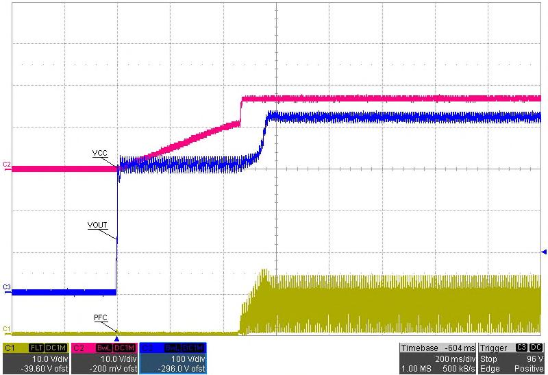
20 VCC (red), VOUT (blue) and gate drive (yellow) during startup at 90 W/20 VAC VCC (red), VOUT (blue) and gate drive (yellow) during startup at 90 W/230 VAC Application Note 20 Revision.0
21 VCC (green), VAUX (red), VZX (blue) and gate drive (yellow) at 90 W/20V AC VCC (green), VAUX (red), VZX (blue) and gate drive (yellow) at 90 W/230 VAC Application Note 2 Revision.0
 at 90 W/20 VAC (yellow)")

22 VOUT ripple (blue), gate drive (yellow) at 90 W/20 VAC VOUT ripple (blue), gate drive (yellow) at 90 W/230 VAC Application Note 22 Revision.0
23 Current sense (red), VBUS (blue), VOUT (green) and gate drive (yellow) startup at 8 W/20 VAC showing over-voltage protection Application Note 23 Revision.0
24 Current sense (red), VBUS (blue), VOUT (green) and gate drive (yellow) startup at 8 W/230 VAC showing over-voltage protection Application Note 24 Revision.0
25 7 Thermal images Thermal images of the top and bottom of the board in open air at room temperature of 25 C measured after 5 minutes operation: Thermal images for 20 VAC, full load (90 W) Thermal images for 230 VAC, full load (90 W) Application Note 25 Revision.0
26 8 Power factor and THD measurements Power factor and THDi at 90 W load Application Note 26 Revision.0
27 Efficiency and power losses at 90 W load Application Note 27 Revision.0
28 Power factor, THDi and harmonics at 90 W load at 20 VAC 0.000% 9.000% 8.000% 7.000% 6.000% 5.000% 4.000% Harmonic Limit 3.000% 2.000%.000% 0.000% Harmonics vs EN class C limits at 90 W load at 20 VAC Application Note 28 Revision.0
29 Power factor, THDi and harmonics at 90 W load at 230 VAC Application Note 29 Revision.0
30 0.000% 9.000% 8.000% 7.000% 6.000% 5.000% 4.000% Harmonic Limit 3.000% 2.000%.000% 0.000% Harmonics vs EN class C limits at 90 W load at 230 VAC Application Note 30 Revision.0
31 9 Conducted EMI test measurements Conducted EMI plot at 90 W load at 20 VAC Conducted EMI plot at 90 W load at 230 VAC Note: Infineon Technologies does not guarantee compliance with any EMI standard. Application Note 3 Revision.0
32 Application Note 32 Revision.0
33 References 0 Conclusion The waveforms in figures 4 and 5 show that the switching frequency is 37 khz at the peak of the AC line at 20 VAC input. At 230 VAC input the frequency increases to 53 kh with an off time of 5 µs, which meets the target value based on the calculated value of LPFC. Switching frequencies match the values calculated from the design tool. Figure 6 shows the peak current reaches 2. A, which matches the result from equation 4 when VACMIN is replaced by 20 VAC. The current sense portion of the signal supplied to the VBUS input shows the effect of CVBUS, which provides low pass filtering to turn the ramp waveform into an approximately triangular signal. This causes the voltages from maximum to average and from minimum to average, to be approximately equal where the average in steady state operation, is the VBUSREG value typically 4. V. Figure 8 shows the sinusoidal envelope of the inductor current indicating correct operation at minimum AC line input of 90 VAC with a peak current of 0.65 V/0.39 Ω matching the calculated value of 2.98 A. Figure 9 shows the cycle by cycle current limiting operating when the line input is reduced to 75 VAC and limiting the peak current to 2.95 A, very close to the calculated value. Start up time is approximately 0.95 seconds at 20 VAC input measuring from switch on until the gate drive first starts up. Another 0.3 seconds is required for the output to reach 420 V. This also matches the predicted value from equation 2. Start up time is reduced to 0.5 seconds at 230 VAC input. Figures 2 and 3 show the voltage (VZX) signal that appears at the auxiliary winding measured at the ZX test point. As expected the positive and negative peak values vary during the AC line input half cycle but the peak to peak value remains constant. As a consequence the voltage at VAUX from the charge pump circuit is very constant over the line voltage range. There is ample headroom for the linear regulaor circuit to supply VCC at 7.3 V over the full range. Head room cannot however be reduced further without compromising start up performance at low line input. Figures 4 and 5 display the output voltage ripple of around 5V, to verify the calculated CBUC value according to equation 3. Figures 6 and 7 demonstrate the over voltage protection function disabling the gate drive output at startup with light load. Under this condition the output voltage over shoots. The thermal images in section 7 show that in open air at worst case low line condition, the inductor temperature rise is less than 25 C, the PFC MOSFET is 30 C with the input bridge reaching the highest temperature with a 45 C rise. In section 8, figure 20 shows that at full load the power factor remains greater than 0.95 over the 90 to 265 VAC input range. The ithd remains below 5 %, provided the input voltage waveform is a pure sine wave as produced by an electronic AC source. Figure 2 show the efficiency is 94% at 20VAC input and 95 % at 230 VAC input at full load. The individual harmonic measurements are shown in table 2 and table 3 to be well within the class C limits of EN at full load at 20 VAC and 230 VAC. Section 9 displays conducted emissions fall within limits over most of the frequency spectrum from 50 khz to 30 MHz exceeding the limit slightly at around 5MHz. This peak is most likely caused by common mode noise possibly due to test setup or the fact that the board is not enclosed in a metal housing with appropriate screening of the PFC MOSFET. It should be noted that these measurements were not made by a certified test lab and are intended only as an indication of performance. References [] IRS2505LPBF µpfc control IC datasheet, Infineon Technologies. [2] Application Note AN-20508_pl6_02 IRS2505L µpfc Control IC Design Guide, Peter B. Green, Helen Ding - Infineon Technologies Application Note 33 Revision.0
34 Revision History Revision History Major changes since the last revision Page or Reference Description of change -- First Release Application Note 34 Revision.0
35 Trademarks of Infineon Technologies AG µhvic, µipm, µpfc, AU-ConvertIR, AURIX, C66, CanPAK, CIPOS, CIPURSE, CoolDP, CoolGaN, COOLiR, CoolMOS, CoolSET, CoolSiC, DAVE, DI-POL, DirectFET, DrBlade, EasyPIM, EconoBRIDGE, EconoDUAL, EconoPACK, EconoPIM, EiceDRIVER, eupec, FCOS, GaNpowIR, HEXFET, HITFET, HybridPACK, imotion, IRAM, ISOFACE, IsoPACK, LEDrivIR, LITIX, MIPAQ, ModSTACK, my-d, NovalithIC, OPTIGA, OptiMOS, ORIGA, PowIRaudio, PowIRStage, PrimePACK, PrimeSTACK, PROFET, PRO-SIL, RASIC, REAL3, SmartLEWIS, SOLID FLASH, SPOC, StrongIRFET, SupIRBuck, TEMPFET, TRENCHSTOP, TriCore, UHVIC, XHP, XMC Trademarks updated November 205 Other Trademarks All referenced product or service names and trademarks are the property of their respective owners. Edition Published by Infineon Technologies AG 8726 Munich, Germany 206 Infineon Technologies AG. All Rights Reserved. Do you have a question about this document? erratum@infineon.com Document reference IMPORTANT NOTICE The information contained in this application note is given as a hint for the implementation of the product only and shall in no event be regarded as a description or warranty of a certain functionality, condition or quality of the product. Before implementation of the product, the recipient of this application note must verify any function and other technical information given herein in the real application. Infineon Technologies hereby disclaims any and all warranties and liabilities of any kind (including without limitation warranties of non-infringement of intellectual property rights of any third party) with respect to any and all information given in this application note. The data contained in this document is exclusively intended for technically trained staff. It is the responsibility of customer s technical departments to evaluate the suitability of the product for the intended application and the completeness of the product information given in this document with respect to such application. For further information on the product, technology, delivery terms and conditions and prices please contact your nearest Infineon Technologies office ( WARNINGS Due to technical requirements products may contain dangerous substances. For information on the types in question please contact your nearest Infineon Technologies office. Except as otherwise explicitly approved by Infineon Technologies in a written document signed by authorized representatives of Infineon Technologies, Infineon Technologies products may not be used in any applications where a failure of the product or any consequences of the use thereof can reasonably be expected to result in personal injury.
The new OptiMOS V
 AN_201610_PL11_001 The new OptiMOS 5 150 V About this document Scope and purpose The new OptiMOS TM 5 150 V shows several improvements. As a result of deep investigations before starting the development
BSP752R. Features. Applications. Smart High-Side Power Switch
 Features Overload protection Current limitation Short circuit protection Thermal shutdown with restart Overvoltage protection (including load dump) Fast demagnetization of inductive loads Reverse battery
IRDC3883 P3V3 user guide
 UG_2062_PL7_02 IRDC3883 P3V3 user guide About this document Scope and purpose The IR3883 is a synchronous buck converter, providing a compact, high performance and flexible solution in a small 3mm X 3
PVI5080NPbF, PVI5080NSPbF
 PVI5080NPbF, PVI5080NSPbF Photovoltaic Isolator Single Channel 5-10 Volt Output General Description The PVI Series Photovoltaic Isolator generates an electrically isolated DC voltage upon receipt of a
Qualified for industrial apllications according to the relevant tests of JEDEC47/20/22. Pin 1
 TVS (Transient Voltage Suppressor) Bi-directional, 5.5 V,.23 pf, 2, RoHS and Halogen Free compliant Features ESD / transient protection according to: - IEC6-4-2 (ESD): ±2 kv (air / contact discharge) -
Qualified for industrial applications according to the relevant tests of JEDEC47/20/22
 Product description NPN silicon planar epitaxial transistor in 4-pin dual-emitter SOT343 package for low noise and low distortion wideband amplifiers. This RF transistor benefits from Infineon long-term
Evaluation Board for DC Motor Control with the IFX9201. This board user manual provides a basic introduction to the hardware of the H-Bridge Kit 2Go.
 - Board User Manual H-Bridge Kit 2Go About this document Scope and purpose This board user manual provides a basic introduction to the hardware of the H-Bridge Kit 2Go. The H-Bridge Kit 2Go is a complete
Orderable Part Number IRL100HS121 PQFN 2mm x 2mm Tape and Reel 4000 IRL100HS121. Typical R DS(on) (m )
 (m )") Target Applications Wireless charging Adapter Telecom Benefits Higher power density designs Higher switching frequency IR MOSFET - Uses OptiMOS TM 5 Chip Reduced parts count wherever 5V supplies are available
Target Applications Wireless charging Adapter Telecom Benefits Higher power density designs Higher switching frequency IR MOSFET - Uses OptiMOS TM 5 Chip Reduced parts count wherever 5V supplies are available
16 W single end cap T8 lighting demo board
 AN_060_PL5_003 6 W single end cap T8 lighting demo board About this document Scope and purpose This document is for a 6 W/70 ma single stage single end cap T8 LED lamp reference using average current control
Quasi-resonant control with XMC1000
 AN_201606_PL30_020 Quasi-resonant control with XMC1000 About this document Scope and purpose This document introduces quasi-resonant control as a technique which enables traditional switched-mode power
IR MOSFET - StrongIRFET
 IR MOSFET - StrongIRFET D V DSS 250V Applications UPS and Inverter applications Half-bridge and full-bridge topologies Resonant mode power supplies DC/DC and AC/DC converters OR-ing and redundant power
IR MOSFET - StrongIRFET
 IR MOSFET - StrongIRFET D V DSS 25V Applications UPS and Inverter applications Half-bridge and full-bridge topologies Resonant mode power supplies DC/DC and AC/DC converters OR-ing and redundant power
IR MOSFET - StrongIRFET
 IR MOSFET - StrongIRFET D V DSS 300V Applications UPS and Inverter applications Half-bridge and full-bridge topologies Resonant mode power supplies DC/DC and AC/DC converters OR-ing and redundant power
IR MOSFET - StrongIRFET
 IR MOSFET - StrongIRFET Applications UPS and Inverter applications Half-bridge and full-bridge topologies Resonant mode power supplies DC/DC and AC/DC converters OR-ing and redundant power switches Brushed
High voltage CoolMOS CE in SOT-223 package
 AN_201603_PL52_016 High voltage CoolMOS CE in SOT-223 package About this document Scope and purpose Nowadays, the package costs of high voltage, high ohmic MOSFETs (metal oxide semiconductor field effect
TLE7268SK, TLE7268LC Application Note
 TLE7268SK, TLE7268LC Application Note Dual LIN Transceiver About this document Scope and purpose This document provides application information for the transceiver TLE7268 from Infineon Technologies AG
I D = 34A 70 T J = 125 C V GS, Gate -to -Source Voltage (V)
") R DS(on), Drain-to -Source On Resistance (m ) R DS (on), Drain-to -Source On Resistance (m ) IR MOSFET DirectFET Power MOSFET Typical values (unless otherwise specified) Quality Requirement Category: Consumer
R DS(on), Drain-to -Source On Resistance (m ) R DS (on), Drain-to -Source On Resistance (m ) IR MOSFET DirectFET Power MOSFET Typical values (unless otherwise specified) Quality Requirement Category: Consumer
Application Note AN-1214
 Application Note LED Buck Converter Design Using the IRS2505L By Ektoras Bakalakos Table of Contents Page 1. Introduction... 2 2. Buck Converter... 2 3. Peak Current Control... 5 4. Zero-Crossing Detection...
24 V ADR Switch Demonstrator
 About this document Scope and purpose This provides a short introduction into the and its application. Intended audience Electrical engineers who are qualified and familiar with the challenges of handling
PDP SWITCH. V DS min 250 V. V DS(Avalanche) typ. 300 V R DS(on) 10V 29 m T J max 175 C. IRFB4332PbF TO-220 Tube 50 IRFB4332PbF
 typ. 300 V R DS(on) 10V 29 m T J max 175 C. IRFB4332PbF TO-220 Tube 50 IRFB4332PbF") PDP SWITCH Feature Advanced Process Technology Key Parameters Optimized for PDP Sustain, Energy Recovery and Pass Switch Applications Low E PULSE Rating to Reduce Power Dissipation in PDP Sustain, Energy
PDP SWITCH Feature Advanced Process Technology Key Parameters Optimized for PDP Sustain, Energy Recovery and Pass Switch Applications Low E PULSE Rating to Reduce Power Dissipation in PDP Sustain, Energy
IRF9530NSPbF IRF9530NLPbF
 IRF9530NSPbF IRF9530NLPbF Benefits Advanced Process Technology Surface Mount (IRF9530NS) Low-profile through-hole(irf9530nl) 175 C Operating Temperature Fast Switching P-Channel Fully Avalanche Rated Lead-Free
SMPS MOSFET IRF6218SPbF
 SMPS MOSFET HEXFET Power MOSFET Applications Reset Switch for Active Clamp Reset DC-DC converters V DSS R DS(on) (max) I D - 150V 150m @ V GS = -V -27A Benefits Low Gate to Drain Charge to Reduce Switching
Full-bridge converter for UPS
 D 2 PAK/D 2 PAK-7 kit About this document This user guide describes the Infineon full-bridge demo board for UPS. The current design considers only the power section including drivers and power devices
Power electronics engineers who want to design gate driving circuits with focus on Enable and Fault functions.
 Application Note AN2015-07 EiceDRIVER Advanced use of pin EN- About this document Scope and purpose This application note targets to explain the function of the EN- pin of the half bridge driver IC in
High voltage CoolMOS P7 superjunction MOSFET in SOT-223 package
 AN_201705_PL52_021 High voltage CoolMOS P7 superjunction MOSFET in SOT-223 package Authors: Jared Huntington Rene Mente Stefan Preimel About this document Scope and purpose Nowadays, the package cost of
Advanced Gate Drive Options for Silicon- Carbide (SiC) MOSFETs using EiceDRIVER
 MOSFETs using EiceDRIVER") AN2017-04 Advanced Gate Drive Options for Silicon- Carbide (SiC) About this document Scope and purpose This application note discusses the basic parameters of silicon-carbide (SiC) MOSFETs and derives
AN2017-04 Advanced Gate Drive Options for Silicon- Carbide (SiC) About this document Scope and purpose This application note discusses the basic parameters of silicon-carbide (SiC) MOSFETs and derives
TLS810B1xxV33. 1 Overview. Ultra Low Quiescent Current Linear Voltage Regulator. Quality Requirement Category: Automotive
 1 Overview Quality Requirement Category: Automotive Features Ultra Low Quiescent Current of 5.5 µa Wide Input Voltage Range of 2.75 V to 42 V Output Current Capacity up to 100 ma Off Mode Current Less
How to drive a unipolar stepper motor with the TLE8110ED
 How to drive a unipolar stepper motor with the TLE8110ED Product Family: Flex Multichannel Low Side Switches About this document Scope and purpose This Application Note demonstrates the behavior of the
IRFB38N20DPbF IRFS38N20DPbF IRFSL38N20DPbF
 IRFB38N20DPbF IRFS38N20DPbF IRFSL38N20DPbF Applications High frequency DC-DC converters Plasma Display Panel Benefits Low Gate-to-Drain Charge to Reduce Switching Losses Fully Characterized Capacitance
IRLI3705NPbF. HEXFET Power MOSFET V DSS 55V. R DS(on) 0.01 I D 52A
 0.01 I D 52A") Logic Level Gate Drive dvanced Process Technology Isolated Package High Voltage Isolation = 2.5KVRMS Sink to Lead Creepage Dist. = 4.8mm Fully valanche Rated Lead-Free HEXFET Power MOSFET V DSS R DS(on)
Logic Level Gate Drive dvanced Process Technology Isolated Package High Voltage Isolation = 2.5KVRMS Sink to Lead Creepage Dist. = 4.8mm Fully valanche Rated Lead-Free HEXFET Power MOSFET V DSS R DS(on)
Boost PFC and SMPS Control IC
 SMPS µpfc TM IRS2505LPBF Boost PFC and SMPS Control IC Features Critical-conduction mode PFC control (CrCM) High PF and ultra-low THD Wide line and load range Regulated DC output voltage No secondary winding
ESD (Electrostatic discharge) sensitive device, observe handling precautions
 sensitive device, observe handling precautions") Product description The BFQ79 is a single stage high linearity high gain driver amplifier based on Infineon's reliable and cost effective NPN silicon germanium technology. Not internally matched, the BFQ79
Product description The BFQ79 is a single stage high linearity high gain driver amplifier based on Infineon's reliable and cost effective NPN silicon germanium technology. Not internally matched, the BFQ79
PCB layout guidelines for MOSFET gate driver
 AN_1801_PL52_1801_132230 PCB layout guidelines for MOSFET gate driver About this document Scope and purpose The PCB layout is essential to the optimal function of the MOSFET gate driver. It is also essential
Application Note AN-1173
 Application Note AN-1173 Power Factor Correction using the IRS500 By Peter B. Green Table of Contents Page 1. Introduction.... Power Factor and THD...3 3. PFC Boost Pre-regulator...5 4. Design Equations...11
TLE4959C Transmission Speed Sensor
 Features Hall based differential speed sensor High magnetic sensitivity Large operating airgap Dynamic self-calibration principle Adaptive hysteresis Direction of rotation detection High vibration suppression
TLF4277-2LD. 1 Overview
 1 Overview Features Integrated Current Monitor Overvoltage, Overtemperature and Overcurrent Detection Adjustable Output Voltage Output Current up to 300 ma Adjustable Output Current Limitation Stable with
160W PFC Evaluation Board with DCM PFC controller TDA and CoolMOS
 Application Note Version 1.0 160W PFC Evaluation Board with DCM PFC controller TDA4863-2 and CoolMOS SPP08N50C3 Power Management & Supply TDA4863-2 SPP08N50C3 Ver1.0, _doc_release> N e v e
Application Note, V1.1, October 2009 EVALPFC2-ICE2PCS W PFC Evaluation Board with CCM PFC controller ICE2PCS01. Power Management & Supply
 Application Note, V1.1, October 2009 EVALPFC2-ICE2PCS01 300W PFC Evaluation Board with CCM PFC controller ICE2PCS01 Power Management & Supply N e v e r s t o p t h i n k i n g. Edition 2009-10-13 Published
About this document. Table of contents. Authors: Omar Harmon (IFAT IPC APS AE) Dr. Vladimir Scarpa (IFAT IPC APS AE) Application Note
 Dr. Vladimir Scarpa (IFAT IPC APS AE) Application Note") 1200 V CoolSiC S ch o ttky Diode Generation 5 Authors: Omar Harmon (IFAT IPC APS AE) Dr. Vladimir Scarpa (IFAT IPC APS AE) Application Note About this document Scope and purpose This document introduces
1200 V CoolSiC S ch o ttky Diode Generation 5 Authors: Omar Harmon (IFAT IPC APS AE) Dr. Vladimir Scarpa (IFAT IPC APS AE) Application Note About this document Scope and purpose This document introduces
Power Management & Supply. Design Note. Version 2.3, August 2002 DN-EVALSF2-ICE2B765P-1. CoolSET 80W 24V Design Note for Adapter using ICE2B765P
 Version 2.3, August 2002 Design Note DN-EVALSF2-ICE2B765P-1 CoolSET 80W 24V Design Note for Adapter using ICE2B765P Author: Rainer Kling Published by Infineon Technologies AG http://www.infineon.com/coolset
BGA123L4 as Low Current Low Noise Amplifier for GNSS Applications in L5/E5 bands
 AN552 BGA123L4 as Low Current Low Noise Amplifier for GNSS Applications About this document Scope and purpose This application note describes Infineon s GNSS MMIC: BGA123L4 a low-current low noise amplifier
UG_201611_PL16_03. 40W isolated PFC Flyback converter based on the IRS2505L IRuFB1. About this document. Akos Hodany, Peter B.
 UG_201611_PL16_03 IRuFB1 Authors: Akos Hodany, Peter B. Green About this document Scope and purpose The purpose of this document is to provide a comprehensive functional description and guide to using
Superjunction MOSFET for charger applications
 AN_201411_PL11_008 Superjunction MOSFET for charger applications About this document Scope and purpose This application note will describe the fundamental differences between a Superjunction MOSFET and
Power Management & Multimarket
 DP10T Diversity Cross Switch for Carrier Aggregation Data Sheet Revision 3.1-2016-11-03 Power Management & Multimarket Edition 2016-11-03 Published by Infineon Technologies AG 81726 Munich, Germany c 2016
Application Note AN-1151
 Application Note AN-1151 IS168D Additional Design Information By T. ibarich Table of Contents Page Introduction... 1 Ballast Oscillator... Circuit..... 4 esonant Tank Output Circuit. 9 IC Start-Up and
SP4T Diversity Antenna Switch with GPIO Interface BGS14GA14
 AN479 SP4T Diversity Antenna Switch with GPIO Interface About this document Scope and purpose This application note describes Infineon s SP4T Diversity Antenna Switch with GPIO Interface: as switch for
SP5T Diversity Antenna Switch with GPIO Interface BGS15GA14
 AN480 SP5T Diversity Antenna Switch with GPIO Interface About this document Scope and purpose This application note describes Infineon s SP5T Diversity Antenna Switch with GPIO Interface: as switch for
Silicon Germanium Low Noise Amplifier BGA7L1BN6
 AN491 Silicon Germanium Low Noise Amplifier BGA7L1BN6 About this document Scope and purpose This application note describes Infineon s MMIC: BGA7L1BN6 as Low Noise Amplifier for LTE Band 28 (758 MHz )
Intended audience This application note is intended for all technical specialists working with the EVAL-M D board.
 AN06-4 EVAL-M-05-84D EVAL-M-05-84D About this document Scope and purpose This application note provides an overview of the evaluation board EVAL-M-05-84D including its main features, key data, pin assignments
Application Note, V2.0, March 2006 EVALPFC2-ICE1PCS W PFC Evaluation Board with CCM PFC controller ICE1PCS01. Power Management & Supply
 Application Note, V2.0, March 2006 EVALPFC2-ICE1PCS01 300W PFC Evaluation Board with CCM PFC controller ICE1PCS01 Power Management & Supply N e v e r s t o p t h i n k i n g. Edition 2006-03-27 Published
SPDT high linearity, high power RF Switch BGS12PN10
 AN497 SPDT high linearity, high power RF Switch About this document Scope and purpose This application note describes Infineon s SPDT high linearity, high power RF Switch: as switch for Mobile phones in
High voltage gate driver IC. 600 V half bridge gate drive IC 2EDL05I06PF 2EDL05I06PJ 2EDL05I06BF 2EDL05N06PF 2EDL05N06PJ. EiceDRIVER Compact
 High voltage gate driver IC 600 V half bridge gate drive IC 2EDL05I06PF 2EDL05I06PJ 2EDL05I06BF 2EDL05N06PF 2EDL05N06PJ EiceDRIVER Compact Final datasheet , 18.08.2016 Final Industrial Power
EMC output filter recommendations for MA120XX(P)
") EMC output filter recommendations for MA120XX(P) About this document Scope and purpose This document provides EMC output filter recommendations that are tailored to the Merus Audio s MA12040, MA12040P,
EMC output filter recommendations for MA120XX(P) About this document Scope and purpose This document provides EMC output filter recommendations that are tailored to the Merus Audio s MA12040, MA12040P,
Application Note, Rev.1.0, November 2010 TLE8366. The Demoboard. Automotive Power
 Application Note, Rev.1.0, November 2010 TLE8366 Automotive Power Table of Contents 1 Abstract...3 2 Introduction...3 3 The Demo board...4 3.1 Quick start...4 3.2 The Schematic...5 3.3 Bill of Material...6
Low Side Switch Shield
 User Manual Low Side Switch Shield About this document Scope and purpose This document describes how to use the Low Side Switch Shield. Intended audience Engineers, hobbyists and students who want to add
Applications of 1EDNx550 single-channel lowside EiceDRIVER with truly differential inputs
 AN_1803_PL52_1804_112257 Applications of 1EDNx550 single-channel lowside EiceDRIVER with About this document Scope and purpose This application note shows the potential of the 1EDNx550 EiceDRIVER family
Wideband SP3T RF Switch for RF diversity or RF band selection applications BGS13S2N9
 AN470 Wideband SP3T RF Switch for RF diversity or RF band BGS13S2N9 About this document Scope and purpose This application note describes Infineon s Wideband SP3T RF Switch for RF diversity or RF band
Improving PFC efficiency using the CoolSiC Schottky diode 650 V G6
 AN_201704_PL52_020 Improving PFC efficiency using the CoolSiC Schottky diode 650 V G6 About this document Scope and purpose This engineering report describes the advantages of using the CoolSiC Schottky
Multi-output high power factor flyback converter design using IRS2982S
 AN_1802_PL16_1803_202736 Multi-output high power factor flyback converter design using IRS2982S Authors: Kali Naraharisetti Peter B. Green About this document Scope and purpose The purpose of this document
Tire Pressure Monitoring Sensor
 TPMS Tire Pressure Monitoring Sensor SP37 Application Note Revision 1.0, 2011-10-11 Sense & Control Edition 2011-12-07 Published by Infineon Technologies AG 81726 Munich, Germany 2011 Infineon Technologies
24V Protected Switch Shield with BTT6030-2EKA and BTT6020-1EKA
 24V Protected Switch Shield with BTT6030-2EKA and BTT6020-1EKA About this document Scope and purpose This document describes how to use the 24V Protected Switch Shield with BTT6030-2EKA and BTT6020-1EKA.
TLF Errata Sheet. Automotive Power. Multi Voltage Safety Micro Processor Supply TLF35584QVVS1 TLF35584QVVS2 TLF35584QKVS1 TLF35584QKVS2
 Multi Voltage Safety Micro Processor Supply TLF35584QVVS1 TLF35584QVVS2 TLF35584QKVS1 TLF35584QKVS2 Errata Sheet Rev. 3.0, 2017-03-17 Automotive Power Table of Contents 1 Overview.......................................................................
IRFR6215PbF IRFU6215PbF
 IRFR625PbF IRFU625PbF P-Channel 75 C Operating Temperature Surface Mount (IRFR625) Straight Lead (IRFU625) dvanced Process Technology Fast Switching Fully valanche Rated Lead-Free Description Fifth Generation
High Current PN Half Bridge with Integrated Driver
 High Current PN Half Bridge with Integrated Driver Industrial & Multi Purpose NovalithIC 1 Overview Quality Requirement Category: Industrial Features Path resistance of max. 12.8 mω @ 25 C (typ. 10.0 mω
Developed for automotive applications. Product qualification according to AEC-Q100.
 Dual / Angle Sensor Features Separate supply pins for and sensor Low current consumption and quick start up 360 contactless angle measurement Output amplitude optimized for circuits with 3.3 V or 5 V supply
TLE4959C FX Flexible Transmission Speed Sensor
 TLE4959C FX Flexible Transmission Speed Sensor Features Hall based differential speed sensor High magnetic sensitivity Large operating airgap Dynamic self-calibration principle Adaptive hysteresis Output
Application Note, V1.0, Nov 2004 ICE3B2565. SMPS Evaluation Board with CoolSET TM ICE3B2565. Power Management & Supply
 Application Note, V1.0, Nov 2004 ICE3B2565 SMPS Evaluation Board with CoolSET TM ICE3B2565 F3 Power Management & Supply N e v e r s t o p t h i n k i n g. Edition 2005-01-13 Published by Infineon Technologies
D e m o B o a r d U s e r s M a n u a l. Demoboard Rev.1.0, Standard Power
 IFX80471SKV D e m o B o a r d U s e r s M a n u a l Demoboard Rev.1.0, 2012-05-15 Standard Power 1 Abstract Note: The following information is given as a guideline for the implementation of the device
High voltage gate driver IC. 600 V half bridge gate drive IC 2EDL23I06PJ 2EDL23N06PJ. EiceDRIVER Compact. <Revision 2.4>,
 High voltage gate driver IC 600 V half bridge gate drive IC 2EDL23I06PJ 2EDL23N06PJ EiceDRIVER Compact Final datasheet , 28.11.2017 Final Industrial Power Control Edition 28.11.2017 Published
Guidelines for CoolSiC MOSFET gate drive voltage window
 AN2018-09 Guidelines for CoolSiC MOSFET gate drive voltage window About this document Infineon strives to enhance electrical systems with comprehensive semiconductor competence. This expertise is revealed
Packages. Product Summary. Features. Typical Applications Switched Mode Power Supplies Electronic Ballasts LED Drivers. Typical Connection Diagram
 February 22, 2012 IRS2500S TRANSITION MODE PFC CONTROL IC Features PFC Control IC Boost or Flyback Converter Modes Critical-conduction / Transition mode operation Over-current protection Static and Dynamic
Power Control ICs EVALLED-TDA4863G-40W. Application Note. Industrial & Multimarket
 Power Control ICs EVALLED-TDA4863G-40W Single Stage High Power Factor Flyback Converter for Offline LED Supply TDA4863G TLE4305G Application Note Revision.0, 00-04-0 Industrial & Multimarket Edition 00-04-0
TLE8250G. 1 Overview. High Speed CAN-Transceiver. Quality Requirement Category: Automotive
 1 Overview Quality Requirement Category: Automotive Features Fully compatible to ISO 11898-2 Wide common mode range for electromagnetic immunity (EMI) Very low electromagnetic emission (EME) Excellent
ILD6150/ILD V buck LED driver IC with high accuracy and efficiency
 AN_1809_PL39_1810_153959 ILD6150/ILD6070 60 V buck LED driver IC with high accuracy and Operation, design guide and performance About this document Scope and purpose This application note introduces Infineon
Developed for automotive applications. Product qualification according to AEC-Q100.
 Features Available as single die and dual die with separate supplies for each die Low current consumption and quick start up 360 contactless angle measurement Output amplitude optimized for circuits with
Fairchild Reference Design
 Fairchild Reference Design www.fairchildsemi.com This reference design supports inclusion of the FSL306LRN. It should be used in conjunction with the FSL306LRN datasheet as well as Fairchild s application
Digital PFC CCM boost converter
 AN_201602_PL30_015 Digital PFC CCM boost converter using XMC1400 microcontroller Robert Valascho Sam Abdel-Rahman About this document Scope and purpose This document introduces a digital control implementation
Low Cost 8W Off-line LED Driver using RT8487
 Application Note AN019 Jun 2014 Low Cost 8W Off-line LED Driver using RT8487 Abstract RT8487 is a boundary mode constant current controller with internal high side driver, which can be used in buck and
CoolMOS C7 Gold + TOLL = A Perfect Combination
 AN_201605_PL52_019 C7 Gold About this document Scope and purpose This document is intended to describe Infineon s new TOLL (TO-Leadless) SMD package for high-voltage applications, fitted with the high
Reference Design Report for a 21W (42V/0.5A) LED Driver Using SFL900
 LED Driver Using SFL900") Reference Design Report for a 21W (42V/0.5A) LED Driver Using SFL900 Specification Application 90-264VAC Input; 42V/0.5A output LED Driver Author Document Number System Engineering Department SFL900_LED
Reference Design Report for a 21W (42V/0.5A) LED Driver Using SFL900 Specification Application 90-264VAC Input; 42V/0.5A output LED Driver Author Document Number System Engineering Department SFL900_LED
Latest fast diode technology tailored to soft switching applications
 AN_201708_PL52_024 600 V CoolMOS CFD7 About this document Scope and purpose The new 600 V CoolMOS TM CFD7 is Infineon s latest high voltage (HV) SJ MOSFET technology with integrated fast body diode. It
TLS10xB0MB Demoboard. Preface Z8F Table of contents
 Preface Scope and purpose This document provides information about the usage of the demoboards for the voltage tracking regulator TLS10xB0MB (PG-SCT595-5 package variant) from Infineon Technologies AG.
About this document. Table of Contents. Application Note
 ILD6150 Advanced Thermal Protection for High Power LEDs with 60V LED Driver IC ILD6150 Application Note About this document Scope and purpose This Application Note introduces Infineon s Hysteritic Buck
Qualified for Automotive Applications. Product Validation according to AEC-Q100/101
 Features 5 V, and variable output voltage Output voltage tolerance ±4% 4 ma current capability Low-drop voltage Inhibit input Very low current consumption Short-circuit-proof Reverse polarity proof Suitable
ILD2035. MR16 3 W Control Board with ILD2035. Application Note AN214. Industrial and Multimarket. Revision: 1.0 Date:
 ILD2035 MR16 3 W Control Board with ILD2035 Application Note AN214 Revision: 1.0 Date: Industrial and Multimarket Edition Published by Infineon Technologies AG 81726 Munich, Germany 2011 Infineon Technologies
Overvoltage at the Buck Converter Output
 Overvoltage at the Buck Converter Output TLE6361 Multi Voltage Processor Power Supply Application Note Rev. 2.01, 2015-04-14 Automotive Power Table of Contents Table of Contents...............................................................
CIPOS IPM Motor Drive Simulator User Manual
 AN 2017-16 CIPOS IPM Motor Drive Simulator User Manual About this document Scope and purpose To provide guidance for the CIPOS IPM Motor Drive Simulator Tool Intended audience Any user that needs help
AND9043/D. An Off-Line, Power Factor Corrected, Buck-Boost Converter for Low Power LED Applications APPLICATION NOTE.
 An Off-Line, Power Factor Corrected, Buck-Boost Converter for Low Power LED Applications Prepared by: Frank Cathell ON Semiconductor Introduction This application note introduces a universal input, off
AN1642 Application note
 Application note VIPower: 5 V buck SMPS with VIPer12A-E Introduction This paper introduces the 5 V output nonisolated SMPS based on STMicroelectronics VIPer12A-E in buck configuration. The power supply
Evaluation Board for CoolSiC Easy1B half-bridge modules
 AN 2017-41 Evaluation Board for CoolSiC Easy1B half-bridge modules Evaluation of CoolSiC MOSFET modules within a bidirectional buck -boost converter About this document Scope and purpose SiC MOSFET based
IPM Motor Drive Simulator User Manual
 AN 2017-16 IPM Motor Drive Simulator User Manual About this document Scope and purpose To provide guidance for the IPM Motor Drive Simulator Tool Intended audience Any user that needs help with IPM Motor
High performance ac-dc notebook PC adapter meets EPA 4 requirements
 High performance ac-dc notebook PC adapter meets EPA 4 requirements Alberto Stroppa, Claudio Spini, Claudio Adragna STMICROELECTRONICS via C. Olivetti Agrate Brianza (MI), Italy Tel.: +39/ (039) 603.6184,
AL8811. Description. Pin Assignments. Features. Applications. Typical Application Diagram. Boost/Buck/Inverting DC-DC CONVERTER AL8811
 Boost/Buck/Inverting DC-DC CONVERTER Description The is a monolithic control circuit containing the primary functions required for DC-to-DC converters. These devices consist of an internal temperature
AN by Dr. Nicolae-Cristian Sintamarean. by Nicolae-Cristian Sintamarean and Marco Püerschel V
 Automotive MOSFETs Current-Handling in Power-Applications by Dr. Nicolae-Cristian Sintamarean by Nicolae-Cristian Sintamarean and Marco Püerschel Application Note V1.0 2015-05 Automotive High Power Edition
FEBFSL336LRN_CS04U07A Evaluation Board. Fairchild Multi-Output Buck Converter. Featured Fairchild Product: FSL336LRN
 User Guide for FEBFSL336LRN_CS04U07A Evaluation Board Fairchild Multi-Output Buck Converter Featured Fairchild Product: FSL336LRN Direct questions or comments about this evaluation board to: Worldwide
AN2447 Application note
 Application note Quasi-resonant flyback converter for low cost set-top box application Introduction This application note describes how to implement a complete solution for a 17 W switch mode power supply
This document is intended for engineers or developers who would like to improve the accuracy of the XMC1000 internal oscillator.
 AP32321 Oscillator handling About this document Scope and purpose This application note describes the calibration of the frequency of the on-chip oscillator in the microcontroller family. Two methods for
CPC9909 Design Considerations
 Application Note: Design Considerations -R0 www.ixysic.com 1 1 Off-line LED Driver using This application note provides general guidelines for designing an off-line LED driver using IXYS Integrated Circuits
Power Management & Supply. Application Note. Version 3.0, Oct AN-EVALSF2-ICE2B765P2-3. CoolSET 80W 24V Evaluation Board using ICE2B765P2
 Version 3.0, Oct. 2003 Application Note AN-EVALSF2-ICE2B765P2-3 CoolSET 80W 24V Evaluation Board using ICE2B765P2 Author: Rainer Kling Published by Infineon Technologies AG http://www.infineon.com/coolset
LOW QUIESCENT CURRENT BACK TO BACK MOSFET DRIVER
 Automotive grade Automotive IC Gate driver AUIR3241S LOW QUIESCENT CURRENT BACK TO BACK MOSFET DRIVER Features Very low quiescent current on and off state Back to back configuration Boost converter with