Prospects of Optical Recording in Tera Era. Han-Ping D. Shieh
|
|
|
- Prosper Harrell
- 6 years ago
- Views:
Transcription

1 Prospects of Optical Recording in Tera Era Han-Ping D. Shieh Inst. of Electro-Optical Engineering Nat l Chiao Tung University Hsinchu, Taiwan hpshieh@cc.nctu.edu.tw

2 Disk Storage Roadmap
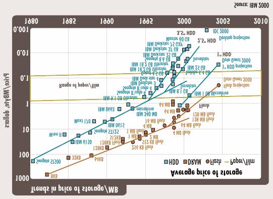
3 $/MB
4 Schematic Diagram of HDD Spindle motor Magnetic W/R head Magnetic disk medium Head suspension??? Base Head actuator VCM (voice coil motor)

5 Magnetic Recording Process
 heads")
6 Write (thin film) & Read (MR & GMR) heads Structures


7 Transitions of magnetic head technology Bulk Head Thin Film Head MR/GMR Head 1979 ~ 1991~ 1998~ Coil Core Write/Read Gap Magnetized Bit Write Head GMR Read Head Write/Read Gap Semiconductor-like/ Micro-fabrication process
8 Super-paramagnetic effect Stability of small- size marks Ferromagnetic state Super-paramagnetic state Energy 40k b T Energy 40k b T E G 0 p 0 k b T < < E G E G = KuV: Magnetic anisotropy energy of crystal K u : Magnetic anisotropy energy constant V: Crystal size (volume) k b : Boltzmann s constant T: temperature E G k b T ~ E G p
9 Optical Disk Storage Status: Density ~ Gb/in 2, Access time ~ 100 msec, Data rate ~ MB/sec, form factor ~ ½ inch, single disk. Optical Diffraction Limit (NA, l)??? Optics, laser, mechanics, electronics, material, etc. integration. Objective: Density ~ Tb/cm 2, access time ~ msec
10 Relationship Between NA and
11 Minimum Recorded Mark Size MO Wmin = σw/mshc or 2 Ddomain wall Wmin 40 nm 20 nm (theory) 45 nm (Exp.) [by Rugar] Wmin 75 nm (MAMMOS using LP - MFM) [by Awano] PC Grain size 5 nm [by Hosaka] 60 nm (SNOM) λ = 785 nm, Pw =7.6 mw/ 5 ms, Pr = 0.2 mw [by Hosaka]

12 Ultra-high Density Storage Roadmap - Reading MR (%) M rt = 1 m emu/cm 2 SNR = 23 db 55 Gb/in 2 : 38 nm 308 nm 350 Gb/in 2 : 18 nm 102 nm 1000 Gb/in 2 : 14 nm 46 nm Year 10
13 Issues in optical detection High-density optical recording by short-wavelength light source Signal Number of photons, Kerr/Faraday rotation angle Number of photons = P RD / (hν) λ Shorter wavelength => Weaker interaction conversion efficiency (A/W) theoretical limit down wavelength (nm) Kerr rotation angle (min.) weaker interaction amorphous GdCo wavelength (nm) Hamamatsu Photonics; Si PIN photo diode, (S ). K. Sato, and Y. Togami; J. Magn. Magn. Mater., 35, (1983), 181.
14 Issues in optical detection Narrow read-power margin by shrinkage optical spot size Upper limit => Read-spot destroys recorded marks. Lower limit => Shot-noise and amp.-noise become dominant. Signal i sign I PD Shot-noise i shot (2qk B I PD ) 1/2 Amp.-noise i amp = const. Other difficulties... Readout signal is strongly affected by quality of optical spot. Developing light source devices of shorter wavelength Many difficulties in optical detection!!! Alternative method: Magnetic Flux detection
 High NA >1 Below-Diffraction-Limit Recording Near-field Recording Probe Recording 3D")
15 2D ultra-high Density Recording Objective Lens Spot Size NA 0.6~0.7 Objective Lens Solid Immerse Lens (SIL) High NA >1 Below-Diffraction-Limit Recording Near-field Recording Probe Recording 3D Storage Multi-function Volumetric optical disks Holographic Memory
16
17 Hybrid Recording Thermal Assist Magnetic Recording Optical head Magnetic coil high readout sensitivity. limitation: High coercive media super-paramagnetic effect perpendicular recording, amorphous materials limitation: Optical diffraction limit low readout sensitivity Hybrid Recording: Optical Writing / Magnetic Reading Recording

18 NIST Awards Thermal Assist Magnetic Recording (HAMR) Seagate, Carnegie Mellon Univ., U. of AZ, MEMS Optical Inc., et al. 5yrs, +20 Millions. Enabling recording density ~ 1000 Gb/in 2
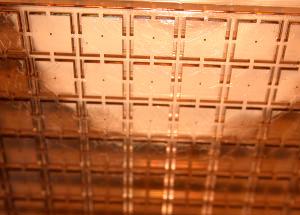
19 Writing Process in Hybrid Recording LS-MFM head Applied field Carbon protective layer Protective layer Conductive layer Protective layer Readout layer Memory layer Protective layer Substrate Requirements of memory layer : 1. Higher Tc 2. High Ku 3. High switching rate Disk rotating direction
20 Reading Process in Hybrid Recording GMR head Output signal Carbon protective layer Protective layer Conductive layer Protective layer Readout layer Memory layer Protective layer Substrate Fringing field Requirements of readout layer : 1. Higher Mr 2. High switching rate
21 Remnant Magnetization (Mr) Requirement in Hybrid Recording 1. CNR log ( V signal /V noise ) V signal M r x mark size x thickness x Dr Dr : the percentage change of resistivity 2. Mr requirement in optical writing/magnetic reading recording 3. CNR of 45 db required for system. Mr (emu/cc) Mark size (um) Thickness (nm) Head sensitivity (compared with MR head) CNR (db) Recording density ( GB/in 2, track width=0.1um) *(1) *(2) Over 100 (1) and (2): IEEE trans. Magn., 36(1), Jan. 2000
22 TbFeCo Dual-layer Media Structure magnetization (emu/cm3) TM-rich 20nm applied field (koe) TM-rich TbFeCo, Ms = 370 emu/cm 3, Mr= 355 emu/cm 3, Hc= 0.95 koe RE-rich TbFeCo, Mr= 113 emu/cm 3, Hc= 4.5 koe SiN 20 nm Readout layer ( h 1 ) Memory layer ( h 2 ) SiN 20 nm Si substrate M t (memu/cm2) memory layer 20 nm/readout layer 20 nm Magnetization reversal of readout layer 6 koe Magnetization reversal of memory layer applied field (koe) Readout layer Hc = 6 koe ( = Hc of single layer + s w /2M 1 h 1 ) NCTU/OSDLAB C.C. Lin
23 Optical Disk Drive

24 Optical Pick-Up by Micro-Optical Bench Technologies
25 Flying Optical Head Slider objective lens, SIL Flying height (air-bearing)< near-field recording Objective Lens slider Solid Immerse Lens (SIL) air bearing < λ disk motion

 Fiberlens output power")
26 Thermal Writing Apparatus by use of Fiberlens Spinning Medium Laser Diode SMF Coupling objective NA=0.2~0.3 Microlens Driver Circuit System throughput efficiency > 50% Laser diode output power (20mW) Fiberlens output power (>10mW) Marks ~1.6 um

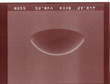
27 Procedure of the Parabolic Lens Making r»60 m NA=0.6
28 Fiberlens-SIL-aperture combination S i O 2 S i substrate Photo resist AZP4620 Step 1: deposit SiO2 as sacrificial layer Step 4: oxide etching Step 7: photolithography mask #2 Photo resist FH6400 Cu Step 2: photolithography mask #1 Step 5: sputtering Cu as seed layer Step 8: reflow Ni SU8 Step 3: reflow Step 6*: electro-plating Ni to reduce aperture Step 9: photolithography mask #3 * Trans Lane and Wensyang Hsu: ISOM01 p252
29 Integrated fiberlens-sil-aperture combination Step 10: release support fiberlens SIL aperture
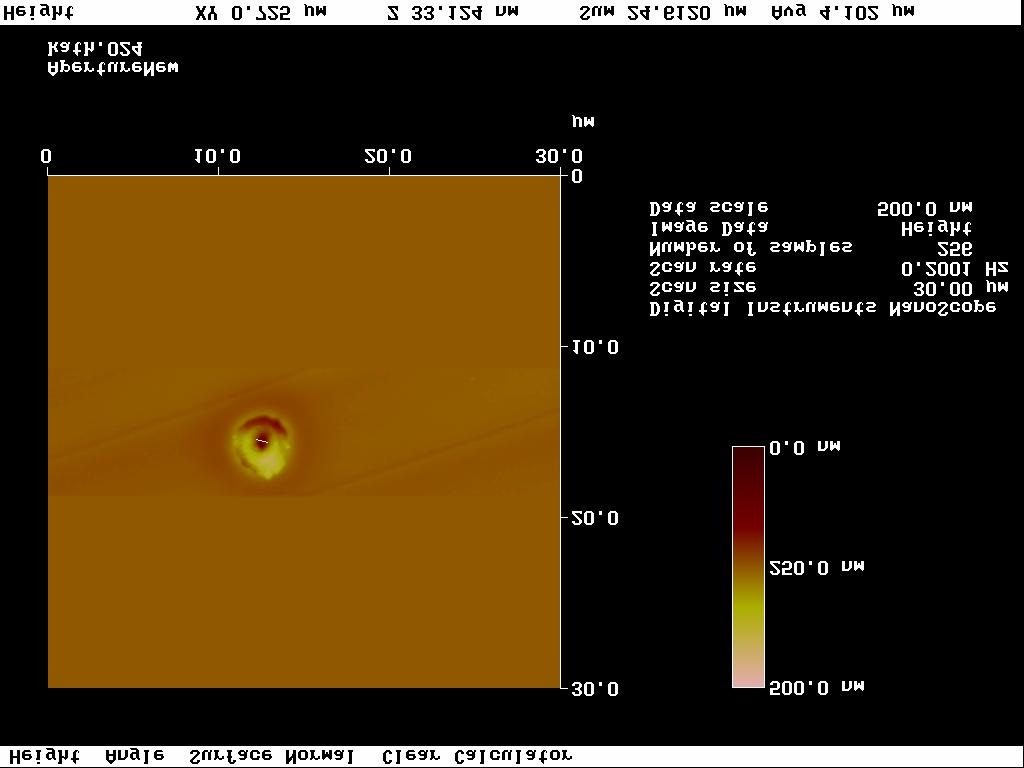
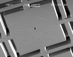
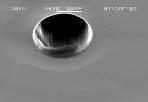
30 Far-field emission light thru sub-um aperture S ~ 600 nm 600 nm AFM image of aperture Far-field emission light thru A sub-um aperture
31 Planar Pick-Up Fiber+Mirror Light Source
32 Planar Pick-up Converge Light Planar Microlens
33 Planar Near-field Aperture Minimize Spot Size Aperture Part
34 Integrated with Thin-Film Magnetic Coils Apply to Thermo-Magnetic Recording Top View Micro Tip Planar Copper Coil Perspective (upside down) A A A-A section
35 Integrated Planar Pick-Up Thermo-Magnetic Recording with GMR Head Planar Thermal-Magnetic Recording GMR Head Recording Layer GMR Head
36 Planar Integrated Pickup for Hybrid Recording focusing mirror formed by isotropic etching or flat mirror formed by anisotropic etching V-groove for fiber alignment fiber lens fiber suspension bonding SIL GMR head for magnetic flux reading planar coil for bias magnetic field Semiconductor-Like Fabrication Processes
37 Disk Storage Perspective Magnetic recording density and data rate are superior and continuously extend beyond forecast. Super paramagnetic limit keeps pushing further. ROM/Write-Once optical storage are very unique for applications. Portable is the niche for erasable optical disks. > 300 Gb/in 2 and beyond, fast access time require more innovation in write/read elements, media, and others. Thermally assisted magnetic/optical (Hybrid) recording using perpendicular media is regarded > Tb/in 2.
Chapter 3 Fabrication
 Chapter 3 Fabrication The total structure of MO pick-up contains four parts: 1. A sub-micro aperture underneath the SIL The sub-micro aperture is used to limit the final spot size from 300nm to 600nm for
HDD Technology Trends
 R e s e a r c h HDD Technology Trends Dr. Richard New Director of Research Hitachi Global Storage Technologies HDD Technology Challenges Storage Technology Capabilities Storage Usage Requirements Storage
Magnetic and Electromagnetic Microsystems. 4. Example: magnetic read/write head
 Magnetic and Electromagnetic Microsystems 1. Magnetic Sensors 2. Magnetic Actuators 3. Electromagnetic Sensors 4. Example: magnetic read/write head (C) Andrei Sazonov 2005, 2006 1 Magnetic microsystems
A-ME technology for linear application
 A-ME technology for linear application Seiichi Onodera Metal Evaporated Product Development Dept. Tape Media Div. Chemical Device Business Group, Sony Corporation 3-4-1 Sakuragi,Tagajo-shi,Miyagi-ken.985-0842
New High Density Recording Technology: Energy Assisted Recording Media
 New High Density Recording Technology: Energy Assisted Recording Yuki Inaba Hitoshi Nakata Daisuke Inoue A B S T R A C T Energy assisted recording, is a next-generation high-density recording technology.
Fabrication and application of a wireless inductance-capacitance coupling microsensor with electroplated high permeability material NiFe
 Journal of Physics: Conference Series Fabrication and application of a wireless inductance-capacitance coupling microsensor with electroplated high permeability material NiFe To cite this article: Y H
MICRO AND NANOPROCESSING TECHNOLOGIES
 MICRO AND NANOPROCESSING TECHNOLOGIES LECTURE 4 Optical lithography Concepts and processes Lithography systems Fundamental limitations and other issues Photoresists Photolithography process Process parameter
Chapter 5. Tracking system with MEMS mirror
 Chapter 5 Tracking system with MEMS mirror Up to now, this project has dealt with the theoretical optimization of the tracking servo with MEMS mirror through the use of simulation models. For these models
Micro-inductors integrated on silicon for power supply on chip
 Journal of Magnetism and Magnetic Materials 316 (27) e233 e237 www.elsevier.com/locate/jmmm Micro-inductors integrated on silicon for power supply on chip Ningning Wang, Terence O Donnell, Saibal Roy,
- Near Field Scanning Optical Microscopy - Electrostatic Force Microscopy - Magnetic Force Microscopy
 - Near Field Scanning Optical Microscopy - Electrostatic Force Microscopy - Magnetic Force Microscopy Yongho Seo Near-field Photonics Group Leader Wonho Jhe Director School of Physics and Center for Near-field
Microscopic Laser Doppler Vibrometer
 Microscopic Laser Doppler Vibrometer System Configuration - 1 PC Controller (APU-Analog processing unit, DPU-Digital processing unit) Optic Head (MEMS Type, XS Type) Function Generator Power Supply Testing
Lithography. 3 rd. lecture: introduction. Prof. Yosi Shacham-Diamand. Fall 2004
 Lithography 3 rd lecture: introduction Prof. Yosi Shacham-Diamand Fall 2004 1 List of content Fundamental principles Characteristics parameters Exposure systems 2 Fundamental principles Aerial Image Exposure
Micro-sensors - what happens when you make "classical" devices "small": MEMS devices and integrated bolometric IR detectors
 Micro-sensors - what happens when you make "classical" devices "small": MEMS devices and integrated bolometric IR detectors Dean P. Neikirk 1 MURI bio-ir sensors kick-off 6/16/98 Where are the targets
Silicon Light Machines Patents
 820 Kifer Road, Sunnyvale, CA 94086 Tel. 408-240-4700 Fax 408-456-0708 www.siliconlight.com Silicon Light Machines Patents USPTO No. US 5,808,797 US 5,841,579 US 5,798,743 US 5,661,592 US 5,629,801 US
Micro-fabrication of Hemispherical Poly-Silicon Shells Standing on Hemispherical Cavities
 Micro-fabrication of Hemispherical Poly-Silicon Shells Standing on Hemispherical Cavities Cheng-Hsuan Lin a, Yi-Chung Lo b, Wensyang Hsu *a a Department of Mechanical Engineering, National Chiao-Tung University,
Optical Interconnection in Silicon LSI
 The Fifth Workshop on Nanoelectronics for Tera-bit Information Processing, 1 st Century COE, Hiroshima University Optical Interconnection in Silicon LSI Shin Yokoyama, Yuichiro Tanushi, and Masato Suzuki
PicoMaster 100. Unprecedented finesse in creating 3D micro structures. UV direct laser writer for maskless lithography
 UV direct laser writer for maskless lithography Unprecedented finesse in creating 3D micro structures Highest resolution in the market utilizing a 405 nm diode laser Structures as small as 300 nm 375 nm
Lecture: Integration of silicon photonics with electronics. Prepared by Jean-Marc FEDELI CEA-LETI
 Lecture: Integration of silicon photonics with electronics Prepared by Jean-Marc FEDELI CEA-LETI Context The goal is to give optical functionalities to electronics integrated circuit (EIC) The objectives
MEMS in ECE at CMU. Gary K. Fedder
 MEMS in ECE at CMU Gary K. Fedder Department of Electrical and Computer Engineering and The Robotics Institute Carnegie Mellon University Pittsburgh, PA 15213-3890 fedder@ece.cmu.edu http://www.ece.cmu.edu/~mems
Practical Applications of Laser Technology for Semiconductor Electronics
 Practical Applications of Laser Technology for Semiconductor Electronics MOPA Single Pass Nanosecond Laser Applications for Semiconductor / Solar / MEMS & General Manufacturing Mark Brodsky US Application
Lecture 22 Optical MEMS (4)
") EEL6935 Advanced MEMS (Spring 2005) Instructor: Dr. Huikai Xie Lecture 22 Optical MEMS (4) Agenda: Refractive Optical Elements Microlenses GRIN Lenses Microprisms Reference: S. Sinzinger and J. Jahns,
EEL6935 Advanced MEMS (Spring 2005) Instructor: Dr. Huikai Xie Lecture 22 Optical MEMS (4) Agenda: Refractive Optical Elements Microlenses GRIN Lenses Microprisms Reference: S. Sinzinger and J. Jahns,
MEMS for RF, Micro Optics and Scanning Probe Nanotechnology Applications
 MEMS for RF, Micro Optics and Scanning Probe Nanotechnology Applications Part I: RF Applications Introductions and Motivations What are RF MEMS? Example Devices RFIC RFIC consists of Active components
Perpendicular Media - Metrology and Inspection Challenges. Sri Venkataram KLA-Tencor Corporation Sept 19, 2007
 Perpendicular Media - Metrology and Inspection Challenges Sri Venkataram KLA-Tencor Corporation Sept 19, 2007 Agenda Perpendicular Media Adoption PMR Metrology & Inspection Implementation Solutions Review
Lecture 7. Lithography and Pattern Transfer. Reading: Chapter 7
 Lecture 7 Lithography and Pattern Transfer Reading: Chapter 7 Used for Pattern transfer into oxides, metals, semiconductors. 3 types of Photoresists (PR): Lithography and Photoresists 1.) Positive: PR
Surface Topography and Alignment Effects in UV-Modified Polyimide Films with Micron Size Patterns
 CHINESE JOURNAL OF PHYSICS VOL. 41, NO. 2 APRIL 2003 Surface Topography and Alignment Effects in UV-Modified Polyimide Films with Micron Size Patterns Ru-Pin Pan 1, Hua-Yu Chiu 1,Yea-FengLin 1,andJ.Y.Huang
Figure 7 Dynamic range expansion of Shack- Hartmann sensor using a spatial-light modulator
 Figure 4 Advantage of having smaller focal spot on CCD with super-fine pixels: Larger focal point compromises the sensitivity, spatial resolution, and accuracy. Figure 1 Typical microlens array for Shack-Hartmann
Outline. 1 Introduction. 2 Basic IC fabrication processes. 3 Fabrication techniques for MEMS. 4 Applications. 5 Mechanics issues on MEMS MDL NTHU
 Outline 1 Introduction 2 Basic IC fabrication processes 3 Fabrication techniques for MEMS 4 Applications 5 Mechanics issues on MEMS 2.2 Lithography Reading: Runyan Chap. 5, or 莊達人 Chap. 7, or Wolf and
Microfabrication technologies for highly-laminated thick metallic cores and 3-D integrated windings
 Microfabrication technologies for highly-laminated thick metallic cores and 3-D integrated windings Florian Herrault Georgia Institute of Technology Atlanta, GA florian@gatech.edu http://mems.gatech.edu/msma
This writeup is adapted from Fall 2002, final project report for by Robert Winsor.
 Optical Waveguides in Andreas G. Andreou This writeup is adapted from Fall 2002, final project report for 520.773 by Robert Winsor. September, 2003 ABSTRACT This lab course is intended to give students
State of the Art Room Temperature Scanning Hall Probe Microscopy using High Performance micro-hall Probes
 State of the Art Room Temperature Scanning Hall Probe Microscopy using High Performance micro-hall Probes A. Sandhu 1, 4, H. Masuda 2, A. Yamada 1, M. Konagai 3, A. Oral 5, S.J Bending 6 RCQEE, Tokyo Inst.
Electronic-Photonic ICs for Low Cost and Scalable Datacenter Solutions
 Electronic-Photonic ICs for Low Cost and Scalable Datacenter Solutions Christoph Theiss, Director Packaging Christoph.Theiss@sicoya.com 1 SEMICON Europe 2016, October 27 2016 Sicoya Overview Spin-off from
Magnetic tunnel junction sensors with conetic alloy. Lei, ZQ; Li, GJ; Egelhoff Jr, WF; Lai, PT; Pong, PWT
 Title Magnetic tunnel junction sensors with conetic alloy Author(s) Lei, ZQ; Li, GJ; Egelhoff Jr, WF; Lai, PT; Pong, PWT Citation The 2010 Asia-Pacific Data Storage Conference (APDSC'10), Hualien, Taiwan,
Defense Technical Information Center Compilation Part Notice
 UNCLASSIFIED Defense Technical Information Center Compilation Part Notice ADP012320 TITLE: Super-Resolution Readout for Magneto-Optical Disk by Optimizing the Deposition Condition of Non-Magnetic Mask
CHAPTER 2 Principle and Design
 CHAPTER 2 Principle and Design The binary and gray-scale microlens will be designed and fabricated. Silicon nitride and photoresist will be taken as the material of the microlens in this thesis. The design
State-of-the-art device fabrication techniques
 State-of-the-art device fabrication techniques! Standard Photo-lithography and e-beam lithography! Advanced lithography techniques used in semiconductor industry Deposition: Thermal evaporation, e-gun
Major Fabrication Steps in MOS Process Flow
 Major Fabrication Steps in MOS Process Flow UV light Mask oxygen Silicon dioxide photoresist exposed photoresist oxide Silicon substrate Oxidation (Field oxide) Photoresist Coating Mask-Wafer Alignment
PERPENDICULAR FILM HEAD PROCESSING PERSPECTIVES FOR AREAL DENSITY INCREASES
 PERPENDICULAR FILM HEAD PROCESSING PERSPECTIVES FOR AREAL DENSITY INCREASES R. E. Fontana, Jr., N. Robertson, M.C. Cyrille, J. Li, J. Katine San Jose Research Center Hitachi Global Storage Technologies
attocube systems Probe Stations for Extreme Environments CRYOGENIC PROBE STATION fundamentals principles of cryogenic probe stations
 PAGE 88 & 2008 2007 PRODUCT CATALOG CRYOGENIC PROBE STATION fundamentals...................... 90 principles of cryogenic probe stations attocps I.......................... 92 ultra stable cryogenic probe
Part 5-1: Lithography
 Part 5-1: Lithography Yao-Joe Yang 1 Pattern Transfer (Patterning) Types of lithography systems: Optical X-ray electron beam writer (non-traditional, no masks) Two-dimensional pattern transfer: limited
Technology Development for a Linear Tape Multi-terabyte terabyte Tape System
 Technology Development for a Linear Tape Multi-terabyte terabyte Tape System (NIST ATP PROGRAM 70NANB2H3040) Ted Schwarz Peregrine Recording Technology 1462 Tamberwood Trail, Woodbury MN 55125-3363 Phone:
MEMS JUMPSTART SERIES: CREATING AN OPTICAL SWITCH NICOLAS WILLIAMS, PRODUCT MARKETING MANAGER, MENTOR GRAPHICS
 MEMS JUMPSTART SERIES: CREATING AN OPTICAL SWITCH NICOLAS WILLIAMS, PRODUCT MARKETING MANAGER, MENTOR GRAPHICS A M S D E S I G N & V E R I F I C A T I O N W H I T E P A P E R w w w. m e n t o r. c o m
64 Channel Flip-Chip Mounted Selectively Oxidized GaAs VCSEL Array
 64 Channel Flip-Chip Mounted Selectively Oxidized GaAs VCSEL Array 69 64 Channel Flip-Chip Mounted Selectively Oxidized GaAs VCSEL Array Roland Jäger and Christian Jung We have designed and fabricated
Examination Optoelectronic Communication Technology. April 11, Name: Student ID number: OCT1 1: OCT 2: OCT 3: OCT 4: Total: Grade:
 Examination Optoelectronic Communication Technology April, 26 Name: Student ID number: OCT : OCT 2: OCT 3: OCT 4: Total: Grade: Declaration of Consent I hereby agree to have my exam results published on
Photolithography II ( Part 2 )
") 1 Photolithography II ( Part 2 ) Chapter 14 : Semiconductor Manufacturing Technology by M. Quirk & J. Serda Saroj Kumar Patra, Department of Electronics and Telecommunication, Norwegian University of Science
1 Photolithography II ( Part 2 ) Chapter 14 : Semiconductor Manufacturing Technology by M. Quirk & J. Serda Saroj Kumar Patra, Department of Electronics and Telecommunication, Norwegian University of Science
Flip chip Assembly with Sub-micron 3D Re-alignment via Solder Surface Tension
 Flip chip Assembly with Sub-micron 3D Re-alignment via Solder Surface Tension Jae-Woong Nah*, Yves Martin, Swetha Kamlapurkar, Sebastian Engelmann, Robert L. Bruce, and Tymon Barwicz IBM T. J. Watson Research
Silicon Photonics Photo-Detector Announcement. Mario Paniccia Intel Fellow Director, Photonics Technology Lab
 Silicon Photonics Photo-Detector Announcement Mario Paniccia Intel Fellow Director, Photonics Technology Lab Agenda Intel s Silicon Photonics Research 40G Modulator Recap 40G Photodetector Announcement
Semiconductor Lasers Semiconductors were originally pumped by lasers or e-beams First diode types developed in 1962: Create a pn junction in
 Semiconductor Lasers Semiconductors were originally pumped by lasers or e-beams First diode types developed in 1962: Create a pn junction in semiconductor material Pumped now with high current density
Microphotonics Readiness for Commercial CMOS Manufacturing. Marco Romagnoli
 Microphotonics Readiness for Commercial CMOS Manufacturing Marco Romagnoli MicroPhotonics Consortium meeting MIT, Cambridge October 15 th, 2012 Passive optical structures based on SOI technology Building
Optical Bus for Intra and Inter-chip Optical Interconnects
 Optical Bus for Intra and Inter-chip Optical Interconnects Xiaolong Wang Omega Optics Inc., Austin, TX Ray T. Chen University of Texas at Austin, Austin, TX Outline Perspective of Optical Backplane Bus
Magnetic Spin Devices: 7 Years From Lab To Product. Jim Daughton, NVE Corporation. Symposium X, MRS 2004 Fall Meeting
 Magnetic Spin Devices: 7 Years From Lab To Product Jim Daughton, NVE Corporation Symposium X, MRS 2004 Fall Meeting Boston, MA December 1, 2004 Outline of Presentation Early Discoveries - 1988 to 1995
plasmonic nanoblock pair
 Nanostructured potential of optical trapping using a plasmonic nanoblock pair Yoshito Tanaka, Shogo Kaneda and Keiji Sasaki* Research Institute for Electronic Science, Hokkaido University, Sapporo 1-2,
Hard Disk Drive Industry Driving Areal Density and Lithography
 Hard Disk Drive Industry Driving Areal Density and Lithography September 18, 2008 Paul Hofemann Molecular Imprints Global Demand for Digital Storage Worldwide population penetration Internet at 20% PC
Integrated Focusing Photoresist Microlenses on AlGaAs Top-Emitting VCSELs
 Integrated Focusing Photoresist Microlenses on AlGaAs Top-Emitting VCSELs Andrea Kroner We present 85 nm wavelength top-emitting vertical-cavity surface-emitting lasers (VCSELs) with integrated photoresist
Micro Precision Apertures
 National Aperture, Inc. Micro Precision Apertures Product Guide Precision apertures, targets and patterns, including round, slit, square, etc., for universal and high power applications National Aperture,
EG2605 Undergraduate Research Opportunities Program. Large Scale Nano Fabrication via Proton Lithography Using Metallic Stencils
 EG2605 Undergraduate Research Opportunities Program Large Scale Nano Fabrication via Proton Lithography Using Metallic Stencils Tan Chuan Fu 1, Jeroen Anton van Kan 2, Pattabiraman Santhana Raman 2, Yao
Using Stock Optics. ECE 5616 Curtis
 Using Stock Optics What shape to use X & Y parameters Please use achromatics Please use camera lens Please use 4F imaging systems Others things Data link Stock Optics Some comments Advantages Time and
Silicon Photonics: A Platform for Integration, Wafer Level Assembly and Packaging
 Silicon Photonics: A Platform for Integration, Wafer Level Assembly and Packaging M. Asghari Kotura Inc April 27 Contents: Who is Kotura Choice of waveguide technology Challenges and merits of Si photonics
Over 100 GB Optical Phase-Change Disc System Realized by Near-Field Technology
 E*PCOS05 Over 100 GB Optical Phase-Change Disc System Realized by Near-Field Technology Ariyoshi Nakaoki, Masataka Shinoda, Kimihiro Saito, Tsutomu Ishimoto, Toshihiro Horigome, Katsuji Takagi*, and Masanobu
InP-based Waveguide Photodetector with Integrated Photon Multiplication
 InP-based Waveguide Photodetector with Integrated Photon Multiplication D.Pasquariello,J.Piprek,D.Lasaosa,andJ.E.Bowers Electrical and Computer Engineering Department University of California, Santa Barbara,
Lecture 6 Fiber Optical Communication Lecture 6, Slide 1
 Lecture 6 Optical transmitters Photon processes in light matter interaction Lasers Lasing conditions The rate equations CW operation Modulation response Noise Light emitting diodes (LED) Power Modulation
attocfm I for Surface Quality Inspection NANOSCOPY APPLICATION NOTE M01 RELATED PRODUCTS G
 APPLICATION NOTE M01 attocfm I for Surface Quality Inspection Confocal microscopes work by scanning a tiny light spot on a sample and by measuring the scattered light in the illuminated volume. First,
High-yield Fabrication Methods for MEMS Tilt Mirror Array for Optical Switches
 : MEMS Device Technologies High-yield Fabrication Methods for MEMS Tilt Mirror Array for Optical Switches Joji Yamaguchi, Tomomi Sakata, Nobuhiro Shimoyama, Hiromu Ishii, Fusao Shimokawa, and Tsuyoshi
High-speed Ge photodetector monolithically integrated with large cross silicon-on-insulator waveguide
 [ APPLIED PHYSICS LETTERS ] High-speed Ge photodetector monolithically integrated with large cross silicon-on-insulator waveguide Dazeng Feng, Shirong Liao, Roshanak Shafiiha. etc Contents 1. Introduction
Integration of Optoelectronic and RF Devices for Applications in Optical Interconnect and Wireless Communication
 Integration of Optoelectronic and RF Devices for Applications in Optical Interconnect and Wireless Communication Zhaoran (Rena) Huang Assistant Professor Department of Electrical, Computer and System Engineering
Kalman Filtering Methods for Semiconductor Manufacturing
 Kalman Filtering Methods for Semiconductor Manufacturing Kameshwar Poolla Mechanical Engineering Electrical Engineering University of California Berkeley Outline Kalman Filtering Overview Ingredients Applications
MICROACTUATED MICRO-XYZ STAGES FOR FREE-SPACE MICRO-OPTICAL BENCH
 MCROACTUATED MCRO-XYZ STAGES FOR FREE-SPACE MCRO-OPTCAL BENCH L. Y. Lin*, J. L. Shen, S. S. Lee, G. D. Su, and M. C. Wu University of California at Los Angeles, Electrical Engineering Department 405 Hilgard
9/28/2010. Chapter , The McGraw-Hill Companies, Inc.
 Chapter 4 Sensors are are used to detect, and often to measure, the magnitude of something. They basically operate by converting mechanical, magnetic, thermal, optical, and chemical variations into electric
A process for, and optical performance of, a low cost Wire Grid Polarizer
 1.0 Introduction A process for, and optical performance of, a low cost Wire Grid Polarizer M.P.C.Watts, M. Little, E. Egan, A. Hochbaum, Chad Jones, S. Stephansen Agoura Technology Low angle shadowed deposition
Semiconductor Lasers Semiconductors were originally pumped by lasers or e-beams First diode types developed in 1962: Create a pn junction in
 Semiconductor Lasers Semiconductors were originally pumped by lasers or e-beams First diode types developed in 1962: Create a pn junction in semiconductor material Pumped now with high current density
EE290C - Spring 2004 Advanced Topics in Circuit Design High-Speed Electrical Interfaces
 EE290C - Spring 2004 Advanced Topics in Circuit Design High-Speed Electrical Interfaces Lecture 23 Case Studies Disk Drive Read/Write Channels Borivoje Nikolić April 13, 2004. Announcements Homework #3
Photo-Electronic Crossbar Switching Network for Multiprocessor Systems
 Photo-Electronic Crossbar Switching Network for Multiprocessor Systems Atsushi Iwata, 1 Takeshi Doi, 1 Makoto Nagata, 1 Shin Yokoyama 2 and Masataka Hirose 1,2 1 Department of Physical Electronics Engineering
Supplementary Information
 Supplementary Information Wireless thin film transistor based on micro magnetic induction coupling antenna Byoung Ok Jun 1, Gwang Jun Lee 1, Jong Gu Kang 1,2, Seung Uk Kim 1, Ji Woong Choi 1, Seung Nam
Section 2: Lithography. Jaeger Chapter 2. EE143 Ali Javey Slide 5-1
 Section 2: Lithography Jaeger Chapter 2 EE143 Ali Javey Slide 5-1 The lithographic process EE143 Ali Javey Slide 5-2 Photolithographic Process (a) (b) (c) (d) (e) (f) (g) Substrate covered with silicon
MICROMACHINED WAVEGUIDE COMPONENTS FOR SUBMILLIMETER-WAVE APPLICATIONS
 MICROMACHINED WAVEGUIDE COMPONENTS FOR SUBMILLIMETER-WAVE APPLICATIONS K. Hui, W.L. Bishop, J.L. Hesler, D.S. Kurtz and T.W. Crowe Department of Electrical Engineering University of Virginia 351 McCormick
SAMPLE SLIDES & COURSE OUTLINE. Core Competency In Semiconductor Technology: 2. FABRICATION. Dr. Theodore (Ted) Dellin
 Dellin") & Digging Deeper Devices, Fabrication & Reliability For More Info:.com or email Dellin@ieee.org SAMPLE SLIDES & COURSE OUTLINE In : 2. A Easy, Effective, of How Devices Are.. Recommended for everyone who
& Digging Deeper Devices, Fabrication & Reliability For More Info:.com or email Dellin@ieee.org SAMPLE SLIDES & COURSE OUTLINE In : 2. A Easy, Effective, of How Devices Are.. Recommended for everyone who
Winter College on Optics: Fundamentals of Photonics - Theory, Devices and Applications February 2014
 2572-10 Winter College on Optics: Fundamentals of Photonics - Theory, Devices and Applications 10-21 February 2014 Photonic packaging and integration technologies II Sonia M. García Blanco University of
Quasi-Phase-Matched Faraday Rotation in Semiconductor Waveguides with a Magneto-Optic Cladding for Monolithically Integrated Optical Isolators
 Quasi-Phase-Matched Faraday Rotation in Semiconductor Waveguides with a Magneto-Optic Cladding for Monolithically Integrated Optical Isolators Prof. David C. Hutchings, Barry M. Holmes and Cui Zhang, Acknowledgements
Semiconductor Optical Communication Components and Devices Lecture 18: Introduction to Diode Lasers - I
 Semiconductor Optical Communication Components and Devices Lecture 18: Introduction to Diode Lasers - I Prof. Utpal Das Professor, Department of lectrical ngineering, Laser Technology Program, Indian Institute
Cost-effective wavelength-tunable fiber laser using self-seeding Fabry-Perot laser diode
 Cost-effective wavelength-tunable fiber laser using self-seeding Fabry-Perot laser diode Chien Hung Yeh, 1* Fu Yuan Shih, 2 Chia Hsuan Wang, 3 Chi Wai Chow, 3 and Sien Chi 2, 3 1 Information and Communications
LOS 1 LASER OPTICS SET
 LOS 1 LASER OPTICS SET Contents 1 Introduction 3 2 Light interference 5 2.1 Light interference on a thin glass plate 6 2.2 Michelson s interferometer 7 3 Light diffraction 13 3.1 Light diffraction on a
The Wave Nature of Light
 The Wave Nature of Light Physics 102 Lecture 7 4 April 2002 Pick up Grating & Foil & Pin 4 Apr 2002 Physics 102 Lecture 7 1 Light acts like a wave! Last week we saw that light travels from place to place
A novel tunable diode laser using volume holographic gratings
 A novel tunable diode laser using volume holographic gratings Christophe Moser *, Lawrence Ho and Frank Havermeyer Ondax, Inc. 85 E. Duarte Road, Monrovia, CA 9116, USA ABSTRACT We have developed a self-aligned
EE119 Introduction to Optical Engineering Spring 2003 Final Exam. Name:
 EE119 Introduction to Optical Engineering Spring 2003 Final Exam Name: SID: CLOSED BOOK. THREE 8 1/2 X 11 SHEETS OF NOTES, AND SCIENTIFIC POCKET CALCULATOR PERMITTED. TIME ALLOTTED: 180 MINUTES Fundamental
OPTICS IN MOTION. Introduction: Competing Technologies: 1 of 6 3/18/2012 6:27 PM.
 1 of 6 3/18/2012 6:27 PM OPTICS IN MOTION STANDARD AND CUSTOM FAST STEERING MIRRORS Home Products Contact Tutorial Navigate Our Site 1) Laser Beam Stabilization to design and build a custom 3.5 x 5 inch,
Development of 14 Gbit/s Uncooled TOSA with Wide Operating Temperature Range
 INFORMATION & COMMUNICATIONS Development of 14 Gbit/s Uncooled TOSA with Wide Operating Temperature Range Shunsuke SATO*, Hayato FUJITA*, Keiji TANAKA, Akihiro MOTO, Masaaki ONO and Tomoya SAEKI The authors
MICROCHIP MANUFACTURING by S. Wolf
 MICROCHIP MANUFACTURING by S. Wolf Chapter 19 LITHOGRAPHY II: IMAGE-FORMATION and OPTICAL HARDWARE 2004 by LATTICE PRESS CHAPTER 19 - CONTENTS Preliminaries: Wave- Motion & The Behavior of Light Resolution
INF 5490 RF MEMS. LN12: RF MEMS inductors. Spring 2011, Oddvar Søråsen Department of informatics, UoO
 INF 5490 RF MEMS LN12: RF MEMS inductors Spring 2011, Oddvar Søråsen Department of informatics, UoO 1 Today s lecture What is an inductor? MEMS -implemented inductors Modeling Different types of RF MEMS
5. Lithography. 1. photolithography intro: overall, clean room 2. principle 3. tools 4. pattern transfer 5. resolution 6. next-gen
 5. Lithography 1. photolithography intro: overall, clean room 2. principle 3. tools 4. pattern transfer 5. resolution 6. next-gen References: Semiconductor Devices: Physics and Technology. 2 nd Ed. SM
Physics of Waveguide Photodetectors with Integrated Amplification
 Physics of Waveguide Photodetectors with Integrated Amplification J. Piprek, D. Lasaosa, D. Pasquariello, and J. E. Bowers Electrical and Computer Engineering Department University of California, Santa
Packaging Roadmap: The impact of miniaturization. Bob Pfahl, inemi Celestica-iNEMI Technology Forum May 15, 2007
 Packaging Roadmap: The impact of miniaturization Bob Pfahl, inemi Celestica-iNEMI Technology Forum May 15, 2007 The Challenges for the Next Decade Addressing the consumer experience using the converged
Experimental study of slider dynamics induced by contacts with disk asperities
 Microsyst Technol (2013) 19:1369 1375 DOI 10.1007/s00542-013-1822-z TECHNICAL PAPER Experimental study of slider dynamics induced by contacts with disk asperities Wenping Song Liane Matthes Andrey Ovcharenko
Fabrication and Usage of a Multi-turn µ-coil and a PR Channel Combined with a Dual-type GMR-SV Device
 Journal of Magnetics 22(4), 649-653 (2017) ISSN (Print) 1226-1750 ISSN (Online) 2233-6656 https://doi.org/10.4283/jmag.2017.22.4.649 Fabrication and Usage of a Multi-turn µ-coil and a PR Channel Combined
Industrialization of Micro-Electro-Mechanical Systems. Werner Weber Infineon Technologies
 Industrialization of Micro-Electro-Mechanical Systems Werner Weber Infineon Technologies Semiconductor-based MEMS market MEMS Market 2004 (total 22.7 BUS$) Others mostly Digital Light Projection IR Sensors
Electroless Bumping for 300mm Wafers
 Electroless Bumping for 300mm Wafers T. Oppert Internepcon 2006 Tokyo Big Sight, Japan Outline Short Company Profile Electroless Ni/Au Under Bump Metallization UBM for Copper Devices Solder Bumping: Stencil
PHGN/CHEN/MLGN 435/535: Interdisciplinary Silicon Processing Laboratory. Simple Si solar Cell!
 Where were we? Simple Si solar Cell! Two Levels of Masks - photoresist, alignment Etch and oxidation to isolate thermal oxide, deposited oxide, wet etching, dry etching, isolation schemes Doping - diffusion/ion
The Lightwave Model 142 CW Visible Ring Laser, Beam Splitter, Model ATM- 80A1 Acousto-Optic Modulator, and Fiber Optic Cable Coupler Optics Project
 The Lightwave Model 142 CW Visible Ring Laser, Beam Splitter, Model ATM- 80A1 Acousto-Optic Modulator, and Fiber Optic Cable Coupler Optics Project Stephen W. Jordan Seth Merritt Optics Project PH 464
Fast, Two-Dimensional Optical Beamscanning by Wavelength Switching T. K. Chan, E. Myslivets, J. E. Ford
 Photonics Systems Integration Lab University of California San Diego Jacobs School of Engineering Fast, Two-Dimensional Optical Beamscanning by Wavelength Switching T. K. Chan, E. Myslivets, J. E. Ford
CLUSTERLINE RAD VERSATILE DYNAMIC SPUTTER SYSTEM OPTOELECTRONICS, MEMS, PHOTONICS, WIRELESS
 CLUSTERLINE RAD VERSATILE DYNAMIC SPUTTER SYSTEM OPTOELECTRONICS, MEMS, PHOTONICS, WIRELESS CLUSTERLINE RAD Enabling your roadmap in thin film deposition The combination of Evatec s process know-how and
High-Speed Scalable Silicon-MoS 2 P-N Heterojunction Photodetectors
 High-Speed Scalable Silicon-MoS 2 P-N Heterojunction Photodetectors Veerendra Dhyani 1, and Samaresh Das 1* 1 Centre for Applied Research in Electronics, Indian Institute of Technology Delhi, New Delhi-110016,
InP-based Waveguide Photodetector with Integrated Photon Multiplication
 InP-based Waveguide Photodetector with Integrated Photon Multiplication D.Pasquariello,J.Piprek,D.Lasaosa,andJ.E.Bowers Electrical and Computer Engineering Department University of California, Santa Barbara,