Inline PL Imaging Techniques for Crystalline Silicon Cell Production. F. Korsós, Z. Kiss, Ch. Defranoux and S. Gaillard
|
|
|
- Marylou Robbins
- 6 years ago
- Views:
Transcription


1 Inline PL Imaging Techniques for Crystalline Silicon Cell Production F. Korsós, Z. Kiss, Ch. Defranoux and S. Gaillard
2 OUTLINE I. Categorization of PL imaging techniques II. PL imaging setups III. Inline PLI for as-cut wafer sorting a) Band-to-band PLI correlation to µ-pcd b) Defect-band PLI IV. Inline PL imaging of passivated surface PV wafers a) Correlation between 2D and Inline PLI b) Correlation to QSS-µPCD J0 V. PL imaging on finished cells a) Defect visualization comparison to EL VI. Summary 2
 Detector (Camera,")

: I 2 PL, B B ~ n(")
: I ~")
3 PL imaging techniques The PL phenomenon hν < hν 0 Light source (hν 0 > E g ) Detector (Camera, diode, spectrograph) And the physics behind E g The PL result by different detector types hν 0 > E g E c hν 2 < E g hν 1 ~ E g hν 3 < E g E v Band-to-band luminescence (ν 1 ): I 2 PL, B B ~ n( Ndop n) ~ a eff b eff From Princeton instruments homepage Defect-band luminescence (ν 1,2 ): I ~ PL, D B N defect 3


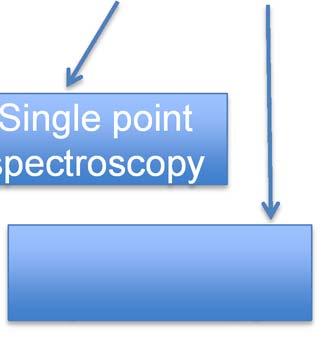


4 Classification of PL measurements techniques Photoluminescence Spectroscopy (λ resolved) Imaging (Integrated in λ) Single point spectroscopy Camera based spectroscopy Scanning On the fly (Line camera based) Imaging by camera Stationary (2D camera) Band to Band PL Defect - Band PL Band to Band PL Defect - Band PL (not for Si CCD) 4
 Inline line camera based setup for as-cut wafes: Moving wafer IR-laser Illumination in a focused stripe InGaAs camera Capability for both")
 Visualization of O rings due to different impact of thermal donors Related publication is in")
5 Inline PL imaging for as-cut wafers 2D camera based setup: Most common imaging setup Stationary wafer position Full wafer illumination steady state conditions Si CCD only B-B PL carrier lifetime imaging Low injection level on as-cut wafers (~1E13cm -3 ) Inline line camera based setup for as-cut wafes: Moving wafer IR-laser Illumination in a focused stripe InGaAs camera Capability for both B-B (lifetime) and Defect Band PL (depends on the applied filter set) Higher injection level (~1E16cm -3 ) comparable to n in solar cells in operation Sharp PL image of moving as-cut wafer within 1s Possible differences due to different injection level: Contrast at grain boundaries (for mc:si) Visualization of O rings due to different impact of thermal donors Related publication is in preparation 5


6 Inline PL imaging for as-cut wafers The primary inline PLI application is the inspection of as-cut mc:si wafers Usually B-B PL photons are captured by applying 1000nm-1300nm bandpass filters So, practically carrier lifetime is imaged F. Korsós, et al. 26th EU-PVSEC 2012 Parabolic relationship between PL signal and carrier lifetime. PL images can be converted into carrier lifetime maps by the application in-site µ-pcd carrier lifetme measurement 6


7 Inline PL imaging for as-cut wafers Material defects detected on the wafers Grain boundaries High recombination rate at grain boundaries Dislocations Contamination along the wafer edges Highly contaminated wafer (top / bottom wafers) 7


8 Inline PL imaging for as-cut wafers Theese defects can be identified and classified Too large defect area means efficiency loss So, maximum reachable efficiency of the cell can be predicted Relative efficiency [%] Efficiency comparison Sample No. Measured relative efficiency Measured Efficiency Efficiency Forecast Efficiency correlation Forecasted relative efficiency Measured Efficiency 8

9 Inline PL imaging for as-cut wafers By applying >1300nm long-pass filters, the defect-band luminescence can be captured. Dislocations emit significant flux of defect-band PL photons. So, they are directly visible in defect PL images. PL spectrum at the dislocation PL spectrum far from dislocation 9

10 Inline PL imaging after passivation process Production of high effiency solar cells requires the control of surface passivation by the measurment of: Carrier lifetime Emitter saturation current Implied Voc PLI is capable to image these quantities, but requires in-situ calibration. QSS-uPCD is applicable for this purpose* Correct measurement needs steady-state conditions. The focused beam inline PL does not suitable. Our patented solution** is the application of an extended steady-state zone around the line captured by the line camera. Inline QSS-PL *F. Korsós et al, 28th EU-PVSEC (2013) **J. Lagowski, et al. US Patent Application 10
11 Inline PL imaging after passivation process Experimental proof of the importance of the steady-state excitation zone Inline QSS-PL give the same PL image as the 2D camera PL which uses full wafer steady state illumination. 11


12 Inline PL imaging after passivation process Inline QSS-PL image can be converted into J oe or V oc map applying calibration by QSS-uPCD measurement 12

 We have found that")


13 Inline PL imaging of finished cells The standard method to detect the metallization defects (shunts, bad fingers) is ElectroLuminscence (EL) We have found that inline PL is suitable for the same purpose but without requiring electrical contact to the wafer. Example PL image Example PL image raw material: contaminatio n wires: shunts, bad fingers 13
14 Inline PL imaging of finished cells Comparison of PL and EL images: Shunts EL : higher current flows through and near the shunts local warming brighter luminescence, PL : uniform illumination, higher current at shunt lower carrier density at the shunts fainter luminescence; inverse features in EL and PL with respect to each other. Inline- PL EL 14
15 Inline PL imaging of finished cells Comparison of PL and EL images: Bad Fingers EL : Higher local resistance lower local carrier injection lower local carrier density fainter luminescence; PL: Decreased conductance removes larger carrier density around the bad finger thinner darkened stripe around the wire and brighter luminescence in its surrounding inverse features in EL and PL with respect to each other. Comparison of PL and EL images: Contamination Lower local lifetime lower carrier concentration lower PL singal in fainter luminescence in both EL and PL resulting the same dark features on the images. Inline- PL EL 15
16 Summary Summary: PL imaging is applicable in each step of solar cell production to identify wafer quality and / or process problems We developed inline PL systems which is capable to do this job within 1s on moving wafers On as-cut wafers B-B PL signal correlates to upcd lifetime. It can be converted to a lifetime image. Crystal defects can be visulaized with high resolution. Based on this bad quality wafers can be sorted out from production The capturing of defect-band PL photons makes possible the direct imaging of specific defects (e.g. dislocations) Proper PL imaging of passivated PV wafers requires the application of steady-state illumination zone. By this accurate PL measurement can be realized in on-the-fly PL configuration as well. Based on the excellent correlation to QSS-uPCD maps, the PL image can be directly converted to Joe and implied Voc maps ON finished cells EL and PL images may differ but both indicates the same metallization failures. 16
Making the Invisible Visible: New Luminescence Inspection Technology for PV Production
 Breaking the limits of solar inspection Making the Invisible Visible: New Luminescence Inspection Technology for PV Production One of the most effective ways of increasing the quality and lowering the
Available online at ScienceDirect. Energy Procedia 92 (2016 ) 10 15
 10 15") Available online at www.sciencedirect.com ScienceDirect Energy Procedia 92 (16 ) 15 6th International Conference on Silicon Photovoltaics, SiliconPV 16 Local solar cell efficiency analysis performed by
Available online at www.sciencedirect.com ScienceDirect Energy Procedia 92 (16 ) 15 6th International Conference on Silicon Photovoltaics, SiliconPV 16 Local solar cell efficiency analysis performed by
Lecture 18: Photodetectors
 Lecture 18: Photodetectors Contents 1 Introduction 1 2 Photodetector principle 2 3 Photoconductor 4 4 Photodiodes 6 4.1 Heterojunction photodiode.................... 8 4.2 Metal-semiconductor photodiode................
Electrical Characterization
 Listing and specification of characterization equipment at ISC Konstanz 30.05.2016 Electrical Characterization µw-pcd (Semilab) PV2000 (Semilab) - spatially resolved minority charge carrier lifetime -diffusion
Characterization using laser-based technique for failure Si PV module
 SAYURI-PV, Tsukuba, 4th Oct, 2016 Characterization using laser-based technique for failure Si PV module Y. Ishikawa, 1 M. A. Islam, 1 K. Noguchi, 1 H. Iida, 2 Y. Takagi, 2 and H. Nakahama 2 1: NAIST, 2:
Characterisation of Photovoltaic Materials and Cells
 Standard Measurement Services and Prices No. Measurement Description Reference 1 Large area, 0.35-sun biased spectral response (SR) 2 Determination of linearity of spectral response with respect to irradiance
ARC PHOTOVOLTAICS CENTRE OF EXCELLENCE ANNUAL REPORT
 ARC 4.6 Photonics and device CHARACTERISATION 4.6.1 Photoluminescence based characterisation of silicon University Staff A/Prof. Thorsten Trupke Project Scientists and Technicians Allen Yee Undergraduate
Solar Cell Parameters and Equivalent Circuit
 9 Solar Cell Parameters and Equivalent Circuit 9.1 External solar cell parameters The main parameters that are used to characterise the performance of solar cells are the peak power P max, the short-circuit
Titelfoto. Advanced Laser Beam Shaping - for Optimized Process Results and Quality Inspection in the PV Production - Maja Thies.
 2010 LIMO Lissotschenko Mikrooptik GmbH www.limo.de Titelfoto Advanced Laser Beam Shaping - for Optimized Process Results and Quality Inspection in the PV Production - Maja Thies Photonics Key Technology
Characterisation of Photovoltaic Materials and Cells
 Standard Measurement Services and Prices Reference 1 Large area, 0.3-sun bias spectral response Wavelength measurement range: 300 1200 nm; Beam power monitoring and compensation; Measurement cell size:
SILICON NANOWIRE HYBRID PHOTOVOLTAICS
 SILICON NANOWIRE HYBRID PHOTOVOLTAICS Erik C. Garnett, Craig Peters, Mark Brongersma, Yi Cui and Mike McGehee Stanford Univeristy, Department of Materials Science, Stanford, CA, USA ABSTRACT Silicon nanowire
Quantitative local current-voltage analysis with different spatiallyresolved camera based techniques of silicon solar cells with cracks
 Quantitative local current-voltage analysis with different spatiallyresolved camera based techniques of silicon solar cells with cracks Tobias M. Pletzer 1,*, Justus I. van Mölken 1, Sven Rißland 2, Brett
On The Detection of Shunts in Silicon Solar Cells by Photo- and Electroluminescence Imaging
 PROGRESS IN PHOTOVOLTAICS: RESEARCH AND APPLICATIONS Prog. Photovolt: Res. Appl. 2008; 16:325 330 Published online 20 November 2007 in Wiley InterScience (www.interscience.wiley.com).803 Research SHORT
3D light microscopy techniques
 3D light microscopy techniques The image of a point is a 3D feature In-focus image Out-of-focus image The image of a point is not a point Point Spread Function (PSF) 1D imaging 2D imaging 3D imaging Resolution
High-speed Micro-crack Detection of Solar Wafers with Variable Thickness
 High-speed Micro-crack Detection of Solar Wafers with Variable Thickness T. W. Teo, Z. Mahdavipour, M. Z. Abdullah School of Electrical and Electronic Engineering Engineering Campus Universiti Sains Malaysia
Introduction to Photovoltaics
 Introduction to Photovoltaics PHYS 4400, Principles and Varieties of Solar Energy Instructor: Randy J. Ellingson The University of Toledo February 24, 2015 Only solar energy Of all the possible sources
Short Wave Infrared (SWIR) Imaging In Machine Vision
 Imaging In Machine Vision") Short Wave Infrared (SWIR) Imaging In Machine Vision Princeton Infrared Technologies, Inc. Martin H. Ettenberg, Ph. D. President martin.ettenberg@princetonirtech.com Ph: +01 609 917 3380 Booth Hall 1 J12
Short Wave Infrared (SWIR) Imaging In Machine Vision Princeton Infrared Technologies, Inc. Martin H. Ettenberg, Ph. D. President martin.ettenberg@princetonirtech.com Ph: +01 609 917 3380 Booth Hall 1 J12
10/14/2009. Semiconductor basics pn junction Solar cell operation Design of silicon solar cell
 PHOTOVOLTAICS Fundamentals PV FUNDAMENTALS Semiconductor basics pn junction Solar cell operation Design of silicon solar cell SEMICONDUCTOR BASICS Allowed energy bands Valence and conduction band Fermi
Cavity QED with quantum dots in semiconductor microcavities
 Cavity QED with quantum dots in semiconductor microcavities M. T. Rakher*, S. Strauf, Y. Choi, N.G. Stolz, K.J. Hennessey, H. Kim, A. Badolato, L.A. Coldren, E.L. Hu, P.M. Petroff, D. Bouwmeester University
Happy birthday PL Imaging!
 Happy birthday PL Imaging! SPREE Seminar 15 December 2016 Contents The importance of good upbringing Born in AUS, a healthy baby! Baby step, finding your place in the world. Now an adolescent, knowing
Loughborough University Institutional Repository. This item was submitted to Loughborough University's Institutional Repository by the/an author.
 Loughborough University Institutional Repository Effects of lateral resistances in photovoltaic cells and full 2-D parameter extraction for the spatially-resolved models using electroluminescence images
Measurement Guide. Solarzentrum Stuttgart GmbH Rotebühlstr. 145, Stuttgart
 Solarzentrum Stuttgart GmbH Rotebühlstr. 145, 70197 Stuttgart www.solarzentrum-stuttgart.com Tel.: +49 (0) 711 31589433 Fax.: +49 (0) 711 31589435 Table of Contents Table of Contents... 1 1 Quick Facts...
Supporting Information
 Copyright WILEY VCH Verlag GmbH & Co. KGaA, 69469 Weinheim, Germany, 2015. Supporting Information for Adv. Energy Mater., DOI: 10.1002/aenm.201501065 Water Ingress in Encapsulated Inverted Organic Solar
By emitter degradation analysis of high power diode laser bars. Outline Part I
 By emitter degradation analysis of high power diode laser bars Eric Larkins and Jens W. Tomm Outline Part I I. 1. Introduction I. 2. Experimental Techniques I. 3. Case Study 1: Strain Threshold for Increased
On the method of photoluminescence spectral intensity ratio imaging of silicon bricks: Advances and limitations
 On the method of photoluminescence spectral intensity ratio imaging of silicon bricks: Advances and limitations Bernhard Mitchell, Jürgen W. Weber, Daniel Walter, Daniel Macdonald, and Thorsten Trupke
What is the highest efficiency Solar Cell?
 What is the highest efficiency Solar Cell? GT CRC Roof-Mounted PV System Largest single PV structure at the time of it s construction for the 1996 Olympic games Produced more than 1 billion watt hrs. of
3D light microscopy techniques
 3D light microscopy techniques The image of a point is a 3D feature In-focus image Out-of-focus image The image of a point is not a point Point Spread Function (PSF) 1D imaging 1 1 2! NA = 0.5! NA 2D imaging
CONFIGURING. Your Spectroscopy System For PEAK PERFORMANCE. A guide to selecting the best Spectrometers, Sources, and Detectors for your application
 CONFIGURING Your Spectroscopy System For PEAK PERFORMANCE A guide to selecting the best Spectrometers, s, and s for your application Spectral Measurement System Spectral Measurement System Spectrograph
Quality Assurance in Solar with the use of I-V Curves
 Quality Assurance in Solar with the use of I-V Curves Eternal Sun Whitepaper Written by: RJ van Vugt Introduction I Installers, wholesalers and other parties use performance tests in order to check on
Development of outdoor luminescence imaging for drone-based PV array inspection
 Aalborg Universitet Development of outdoor luminescence imaging for drone-based PV array inspection Benatto, Gisele Alves dos Reis; Riedel, Nicholas; Thorsteinsson, Sune; Poulsen, Peter; Thorseth, Anders;
Applications of Steady-state Multichannel Spectroscopy in the Visible and NIR Spectral Region
 Feature Article JY Division I nformation Optical Spectroscopy Applications of Steady-state Multichannel Spectroscopy in the Visible and NIR Spectral Region Raymond Pini, Salvatore Atzeni Abstract Multichannel
Microscopic Structures
 Microscopic Structures Image Analysis Metal, 3D Image (Red-Green) The microscopic methods range from dark field / bright field microscopy through polarisation- and inverse microscopy to techniques like
Evaluation of laser-based active thermography for the inspection of optoelectronic devices
 More info about this article: http://www.ndt.net/?id=15849 Evaluation of laser-based active thermography for the inspection of optoelectronic devices by E. Kollorz, M. Boehnel, S. Mohr, W. Holub, U. Hassler
OPTOELECTRONIC and PHOTOVOLTAIC DEVICES
 OPTOELECTRONIC and PHOTOVOLTAIC DEVICES Outline 1. Introduction to the (semiconductor) physics: energy bands, charge carriers, semiconductors, p-n junction, materials, etc. 2. Light emitting diodes Light
photolithographic techniques (1). Molybdenum electrodes (50 nm thick) are deposited by
. Molybdenum electrodes (50 nm thick) are deposited by") Supporting online material Materials and Methods Single-walled carbon nanotube (SWNT) devices are fabricated using standard photolithographic techniques (1). Molybdenum electrodes (50 nm thick) are deposited
Supporting online material Materials and Methods Single-walled carbon nanotube (SWNT) devices are fabricated using standard photolithographic techniques (1). Molybdenum electrodes (50 nm thick) are deposited
Solar Cells, Modules, Arrays, and Characterization
 ... energizing Ohio for the 21st Century Solar Cells, Modules, Arrays, and Characterization April 17, 2014 The University of Toledo, Department of Physics and Astronomy SSARE, PVIC Principles and Varieties
Supplementary information for: Surface passivated GaAsP single-nanowire solar cells exceeding 10% efficiency grown on silicon
 Supplementary information for: Surface passivated GaAsP single-nanowire solar cells exceeding 10% efficiency grown on silicon Jeppe V. Holm 1, Henrik I. Jørgensen 1, Peter Krogstrup 2, Jesper Nygård 2,4,
Development of a solar cell spectral response mapping system using multi-lbic excitation
 Loughborough University Institutional Repository Development of a solar cell spectral response mapping system using multi-lbic excitation This item was submitted to Loughborough University's Institutional
Quantum Efficiency Measurement System with Internal Quantum Efficiency Upgrade
 Quantum Efficiency Measurement System with Internal Quantum Efficiency Upgrade QE / IPCE SYSTEM Upgraded with Advanced Features Includes IV Testing, Spectral Response, Quantum Efficiency System/ IPCE System
Lab Report 3: Speckle Interferometry LIN PEI-YING, BAIG JOVERIA
 Lab Report 3: Speckle Interferometry LIN PEI-YING, BAIG JOVERIA Abstract: Speckle interferometry (SI) has become a complete technique over the past couple of years and is widely used in many branches of
1 Semiconductor-Photon Interaction
 1 SEMICONDUCTOR-PHOTON INTERACTION 1 1 Semiconductor-Photon Interaction Absorption: photo-detectors, solar cells, radiation sensors. Radiative transitions: light emitting diodes, displays. Stimulated emission:
Fall 2004 Dawn Hettelsater, Yan Zhang and Ali Shakouri, 05/09/2002
 University of California at Santa Cruz Jack Baskin School of Engineering Electrical Engineering Department EE-145L: Properties of Materials Laboratory Lab 6: Solar Cells Fall 2004 Dawn Hettelsater, Yan
Standard Operating Procedure Sinton WCT 120 Photo-conductance Lifetime tester & Suns-V OC Stage
 Standard Operating Procedure Sinton WCT 120 Photo-conductance Lifetime tester & Suns-V OC Stage The system consists of two stages one for Lifetime tester and another for Suns-V OC measurement. Assembly
EQE Measurements in Mid-Infrared Superlattice Structures
 University of Iowa Honors Theses University of Iowa Honors Program Spring 2018 EQE Measurements in Mid-Infrared Superlattice Structures Andrew Muellerleile Follow this and additional works at: http://ir.uiowa.edu/honors_theses
Instruction manual and data sheet ipca h
 1/15 instruction manual ipca-21-05-1000-800-h Instruction manual and data sheet ipca-21-05-1000-800-h Broad area interdigital photoconductive THz antenna with microlens array and hyperhemispherical silicon
Fundamentals of CMOS Image Sensors
 CHAPTER 2 Fundamentals of CMOS Image Sensors Mixed-Signal IC Design for Image Sensor 2-1 Outline Photoelectric Effect Photodetectors CMOS Image Sensor(CIS) Array Architecture CIS Peripherals Design Considerations
Dr. Ralf Freiberger. TEMA GmbH / Mühlbauer Group
 Welcome to ADF&PCD Paris 2018 Inline Final Inspection of Aerosol Cans Dr. Ralf Freiberger TEMA GmbH / Mühlbauer Group Overview 1. Purpose 2. State of the Art: Integration in Line 3. New: Inspection at
Functional Materials. Optoelectronic devices
 Functional Materials Lecture 2: Optoelectronic materials and devices (inorganic). Photonic materials Optoelectronic devices Light-emitting diode (LED) displays Photodiode and Solar cell Photoconductive
Introduction Fundamentals of laser Types of lasers Semiconductor lasers
 ECE 5368 Introduction Fundamentals of laser Types of lasers Semiconductor lasers Introduction Fundamentals of laser Types of lasers Semiconductor lasers How many types of lasers? Many many depending on
Instructions for the Experiment
 Instructions for the Experiment Excitonic States in Atomically Thin Semiconductors 1. Introduction Alongside with electrical measurements, optical measurements are an indispensable tool for the study of
Lecture 19 Optical Characterization 1
 Lecture 19 Optical Characterization 1 1/60 Announcements Homework 5/6: Is online now. Due Wednesday May 30th at 10:00am. I will return it the following Wednesday (6 th June). Homework 6/6: Will be online
Resolution. Diffraction from apertures limits resolution. Rayleigh criterion θ Rayleigh = 1.22 λ/d 1 peak at 2 nd minimum. θ f D
 Microscopy Outline 1. Resolution and Simple Optical Microscope 2. Contrast enhancement: Dark field, Fluorescence (Chelsea & Peter), Phase Contrast, DIC 3. Newer Methods: Scanning Tunneling microscopy (STM),
Chapter 4. Impact of Dust on Solar PV Module: Experimental Analysis
 Chapter 4 Impact of Dust on Solar PV Module: Experimental Analysis 53 CHAPTER 4 IMPACT OF DUST ON SOLAR PV MODULE: EXPERIMENTAL ANALYSIS 4.1 INTRODUCTION: On a bright, sunny day the sun shines approximately
Add CLUE to your SEM. High-efficiency CL signal-collection. Designed for your SEM and application. Maintains original SEM functionality
 Add CLUE to your SEM Designed for your SEM and application The CLUE family offers dedicated CL systems for imaging and spectroscopic analysis suitable for most SEMs. In addition, when combined with other
Copyright 2000 Society of Photo Instrumentation Engineers.
 Copyright 2000 Society of Photo Instrumentation Engineers. This paper was published in SPIE Proceedings, Volume 4043 and is made available as an electronic reprint with permission of SPIE. One print or
Fast Laser Raman Microscope RAMAN
 Fast Laser Raman Microscope RAMAN - 11 www.nanophoton.jp Fast Raman Imaging A New Generation of Raman Microscope RAMAN-11 developed by Nanophoton was created by combining confocal laser microscope technology
Vision Lighting Seminar
 Creators of Evenlite Vision Lighting Seminar Daryl Martin Midwest Sales & Support Manager Advanced illumination 734-213 213-13121312 dmartin@advill.com www.advill.com 2005 1 Objectives Lighting Source
SOLAR CELL INSPECTION WITH RAPTOR PHOTONICS OWL (SWIR) AND FALCON (EMCCD)
 AND FALCON (EMCCD)") Technical Note Solar Cell Inspection SOLAR CELL INSPECTION WITH RAPTOR PHOTONICS OWL (SWIR) AND FALCON (EMCCD) August 2012, Northern Ireland Solar cell inspection relies on imaging the photoluminescence
Technical Note Solar Cell Inspection SOLAR CELL INSPECTION WITH RAPTOR PHOTONICS OWL (SWIR) AND FALCON (EMCCD) August 2012, Northern Ireland Solar cell inspection relies on imaging the photoluminescence
CONTENTS. 2.2 Schrodinger's Wave Equation 31. PART I Semiconductor Material Properties. 2.3 Applications of Schrodinger's Wave Equation 34
 CONTENTS Preface x Prologue Semiconductors and the Integrated Circuit xvii PART I Semiconductor Material Properties CHAPTER 1 The Crystal Structure of Solids 1 1.0 Preview 1 1.1 Semiconductor Materials
We are IntechOpen, the world s leading publisher of Open Access books Built by scientists, for scientists. International authors and editors
 We are IntechOpen, the world s leading publisher of Open Access books Built by scientists, for scientists 3,800 116,000 120M Open access books available International authors and editors Downloads Our
Solar Simulation Standards and QuickSun Measurement System. Antti Tolvanen Endeas Oy
 Solar Simulation Standards and QuickSun Measurement System Antti Tolvanen Endeas Oy 1 Endeas in Brief QuickSun Solar Simulators Technology invented 1996 in Fortum (www.fortum.com) Endeas Oy licenses technology
Problem 4 Consider a GaAs p-n + junction LED with the following parameters at 300 K: Electron diusion coecient, D n = 25 cm 2 =s Hole diusion coecient
 Prof. Jasprit Singh Fall 2001 EECS 320 Homework 7 This homework is due on November 8. Problem 1 An optical power density of 1W/cm 2 is incident on a GaAs sample. The photon energy is 2.0 ev and there is
Initial solar cell characterisation test and comparison with a LED-based solar simulator with variable flash speed and spectrum
 Loughborough University Institutional Repository Initial solar cell characterisation test and comparison with a LED-based solar simulator with variable flash speed and spectrum This item was submitted
An Evaluation of Constituents in Paste for Silicon Solar Cells with Floating Contact Method: A Case Study of Tellurium Oxide
 7 th Metallization Workshop, Konstanz, Germany, 2017 An Evaluation of Constituents in Paste for Silicon Solar Cells with Floating Contact Method: A Case Study of Tellurium Oxide Takayuki Aoyama 1, 2, Mari
Spectroscopy of Ruby Fluorescence Physics Advanced Physics Lab - Summer 2018 Don Heiman, Northeastern University, 1/12/2018
 1 Spectroscopy of Ruby Fluorescence Physics 3600 - Advanced Physics Lab - Summer 2018 Don Heiman, Northeastern University, 1/12/2018 I. INTRODUCTION The laser was invented in May 1960 by Theodor Maiman.
Lab VIII Photodetectors ECE 476
 Lab VIII Photodetectors ECE 476 I. Purpose The electrical and optical properties of various photodetectors will be investigated. II. Background Photodiode A photodiode is a standard diode packaged so that
LEDs, Photodetectors and Solar Cells
 LEDs, Photodetectors and Solar Cells Chapter 7 (Parker) ELEC 424 John Peeples Why the Interest in Photons? Answer: Momentum and Radiation High electrical current density destroys minute polysilicon and
OPTI510R: Photonics. Khanh Kieu College of Optical Sciences, University of Arizona Meinel building R.626
 OPTI510R: Photonics Khanh Kieu College of Optical Sciences, University of Arizona kkieu@optics.arizona.edu Meinel building R.626 Photodetectors Introduction Most important characteristics Photodetector
SUPPLEMENTARY INFORMATION
 In the format provided by the authors and unedited. Photon-triggered nanowire transistors Jungkil Kim, Hoo-Cheol Lee, Kyoung-Ho Kim, Min-Soo Hwang, Jin-Sung Park, Jung Min Lee, Jae-Pil So, Jae-Hyuck Choi,
Real time plasma etch control by means of physical plasma parameters with HERCULES
 Real time plasma etch control by means of physical plasma parameters with HERCULES A. Steinbach 1) S. Bernhard 1) M. Sussiek 4) S. Wurm 2) Ch. Koelbl 3) D. Knobloch 1) Siemens, Dresden Siemens at International
Solar Cell I-V Characteristics
 Chapter 3 Solar Cell I-V Characteristics It is well known that the behaviour of a PhotoVoltaic PV) System is greatly influenced by factors such as the solar irradiance availability and distribution and
Quantum Condensed Matter Physics Lecture 16
 Quantum Condensed Matter Physics Lecture 16 David Ritchie QCMP Lent/Easter 2018 http://www.sp.phy.cam.ac.uk/drp2/home 16.1 Quantum Condensed Matter Physics 1. Classical and Semi-classical models for electrons
SUPPLEMENTARY INFORMATION
 Optically reconfigurable metasurfaces and photonic devices based on phase change materials S1: Schematic diagram of the experimental setup. A Ti-Sapphire femtosecond laser (Coherent Chameleon Vision S)
Chemistry 524--"Hour Exam"--Keiderling Mar. 19, pm SES
 Chemistry 524--"Hour Exam"--Keiderling Mar. 19, 2013 -- 2-4 pm -- 170 SES Please answer all questions in the answer book provided. Calculators, rulers, pens and pencils permitted. No open books allowed.
Emitter profile tailoring to contact homogeneous high sheet resistance emitter
 Vailable online at www.sciencedirect.com Energy Procedia 27 (2012 ) 432 437 Silicon PV: 03-05 April 2012, Leuven, Belgium Emitter profile tailoring to contact homogeneous high sheet resistance emitter
Luminous Equivalent of Radiation
 Intensity vs λ Luminous Equivalent of Radiation When the spectral power (p(λ) for GaP-ZnO diode has a peak at 0.69µm) is combined with the eye-sensitivity curve a peak response at 0.65µm is obtained with
Available online at ScienceDirect. Energy Procedia 92 (2016 )
") Available online at www.sciencedirect.com ScienceDirect Energy Procedia 92 (2016 ) 386 391 6th International Conference on Silicon Photovoltaics, SiliconPV 2016 Effect of diamond wire saw marks on solar
Available online at www.sciencedirect.com ScienceDirect Energy Procedia 92 (2016 ) 386 391 6th International Conference on Silicon Photovoltaics, SiliconPV 2016 Effect of diamond wire saw marks on solar
Characterization of SiPMs for Large Scale Applications
 SiPM KETEK SiPM Characterization of SiPMs for Large Scale Applications Eugen Engelmann (eugen.engelmann@ketek.net) 1 SiPM KETEK Family-owned enterprise, founded in 1989 by Dr. Josef Kemmer Number of employees:
Dual-FL. World's Fastest Fluorometer. Measure absorbance spectra and fluorescence simultaneously FLUORESCENCE
 Dual-FL World's Fastest Fluorometer Measure absorbance spectra and fluorescence simultaneously FLUORESCENCE 100 Times Faster Data Collection The only simultaneous absorbance and fluorescence system available
Observational Astronomy
 Observational Astronomy Instruments The telescope- instruments combination forms a tightly coupled system: Telescope = collecting photons and forming an image Instruments = registering and analyzing the
Key Questions ECE 340 Lecture 28 : Photodiodes
 Things you should know when you leave Key Questions ECE 340 Lecture 28 : Photodiodes Class Outline: How do the I-V characteristics change with illumination? How do solar cells operate? How do photodiodes
Optical design of a low concentrator photovoltaic module
 Optical design of a low concentrator photovoltaic module MA Benecke*, JD Gerber, FJ Vorster and EE van Dyk Nelson Mandela Metropolitan University Centre for Renewable and Sustainable Energy Studies Abstract
SUPPLEMENTARY INFORMATION
 Electrically pumped continuous-wave III V quantum dot lasers on silicon Siming Chen 1 *, Wei Li 2, Jiang Wu 1, Qi Jiang 1, Mingchu Tang 1, Samuel Shutts 3, Stella N. Elliott 3, Angela Sobiesierski 3, Alwyn
Nanowires for Quantum Optics
 Nanowires for Quantum Optics N. Akopian 1, E. Bakkers 1, J.C. Harmand 2, R. Heeres 1, M. v Kouwen 1, G. Patriarche 2, M. E. Reimer 1, M. v Weert 1, L. Kouwenhoven 1, V. Zwiller 1 1 Quantum Transport, Kavli
Thermal management and thermal properties of high-brightness diode lasers
 Thermal management and thermal properties of high-brightness diode lasers Jens W. Tomm Max-Born-Institut für Nichtlineare Optik und Kurzzeitspektroskopie Berlin Max-Born-Str. 2 A, D-12489 Berlin, Germany
Characterisation of SiPM Index :
 Characterisation of SiPM --------------------------------------------------------------------------------------------Index : 1. Basics of SiPM* 2. SiPM module 3. Working principle 4. Experimental setup
Lecture 8 Optical Sensing. ECE 5900/6900 Fundamentals of Sensor Design
 ECE 5900/6900: Fundamentals of Sensor Design Lecture 8 Optical Sensing 1 Optical Sensing Q: What are we measuring? A: Electromagnetic radiation labeled as Ultraviolet (UV), visible, or near,mid-, far-infrared
Technical Notes. Integrating Sphere Measurement Part II: Calibration. Introduction. Calibration
 Technical Notes Integrating Sphere Measurement Part II: Calibration This Technical Note is Part II in a three part series examining the proper maintenance and use of integrating sphere light measurement
Evaluation of high power laser diodes for space applications: effects of the gaseous environment
 Evaluation of high power laser diodes for space applications: effects of the gaseous environment Jorge Piris, E. M. Murphy, B. Sarti European Space Agency, Optoelectronics section, ESTEC. M. Levi, G. Klumel,
LEP Optical pumping
 Related topics Spontaeous emission, induced emission, mean lifetime of a metastable state, relaxation, inversion, diode laser. Principle and task The visible light of a semiconductor diode laser is used
SOLARONIX. Solixon A-1525-V
 SOLARONIX Solixon A-1525-V Based on Solaronix' exclusive light engine, our solar simulation equipment delivers a perfect and continuous artificial sunlight 24/7, allowing for accurate stability and performance
Chapter 3 OPTICAL SOURCES AND DETECTORS
 Chapter 3 OPTICAL SOURCES AND DETECTORS 3. Optical sources and Detectors 3.1 Introduction: The success of light wave communications and optical fiber sensors is due to the result of two technological breakthroughs.
Characterization of EVA degradation processes in Si-based PV modules by means of spatially-resolved luminescence spectroscopy
 Characterization of EVA degradation processes in Si-based PV modules by means of spatially-resolved luminescence spectroscopy 1 Degradation of PV modules Typical construction of a c-si PV module Frontglass
In the name of God, the most merciful Electromagnetic Radiation Measurement
 In the name of God, the most merciful Electromagnetic Radiation Measurement In these slides, many figures have been taken from the Internet during my search in Google. Due to the lack of space and diversity
Components of Optical Instruments. Chapter 7_III UV, Visible and IR Instruments
 Components of Optical Instruments Chapter 7_III UV, Visible and IR Instruments 1 Grating Monochromators Principle of operation: Diffraction Diffraction sources: grooves on a reflecting surface Fabrication:
Properties of a Detector
 Properties of a Detector Quantum Efficiency fraction of photons detected wavelength and spatially dependent Dynamic Range difference between lowest and highest measurable flux Linearity detection rate
ECE 340 Lecture 29 : LEDs and Lasers Class Outline:
 ECE 340 Lecture 29 : LEDs and Lasers Class Outline: Light Emitting Diodes Lasers Semiconductor Lasers Things you should know when you leave Key Questions What is an LED and how does it work? How does a
Received 31 January 2007; Revised 21 March 2007
 PROGRESS IN PHOTOVOLTAICS: RESEARCH AND APPLICATIONS Prog. Photovolt: Res. Appl. 2007; 15:613 620 Published online 8 May 2007 in Wiley InterScience (www.interscience.wiley.com).766 Research SHORT COMMUNICATION
Marten Bosma 1, Alex Fauler 2, Michael Fiederle 2 en Jan Visser Nikhef, Amsterdam, The Netherlands 2. FMF, Freiburg, Germany
 Marten Bosma 1, Alex Fauler 2, Michael Fiederle 2 en Jan Visser 1 1. Nikhef, Amsterdam, The Netherlands 2. FMF, Freiburg, Germany Digital Screen film Digital radiography advantages: Larger dynamic range
Coherent Receivers Principles Downconversion
 Coherent Receivers Principles Downconversion Heterodyne receivers mix signals of different frequency; if two such signals are added together, they beat against each other. The resulting signal contains