Dr. Ralf Freiberger. TEMA GmbH / Mühlbauer Group
|
|
|
- Everett Ray
- 5 years ago
- Views:
Transcription


1 Welcome to ADF&PCD Paris 2018

2 Inline Final Inspection of Aerosol Cans Dr. Ralf Freiberger TEMA GmbH / Mühlbauer Group

3 Overview 1. Purpose 2. State of the Art: Integration in Line 3. New: Inspection at End of Line 4. Summary


4 Purpose A can is nowadays more than a simple container! The cans have now become - highly resource-conserving - efficient - almost freely designable objects due to new findings from materials science
5 Purpose Higher throughputs new materials (recycled aluminum) Thinner wall thickness More complex shapes (more inelastic transformations) More critical defects, even smallest defects have to be avoided! Challenge for better defect inspections! Choice of right image processing technology makes it possible for production window of forming process to be used with maximum efficiency in terms of manufacturability!
6 State of the Art: Integration in Line
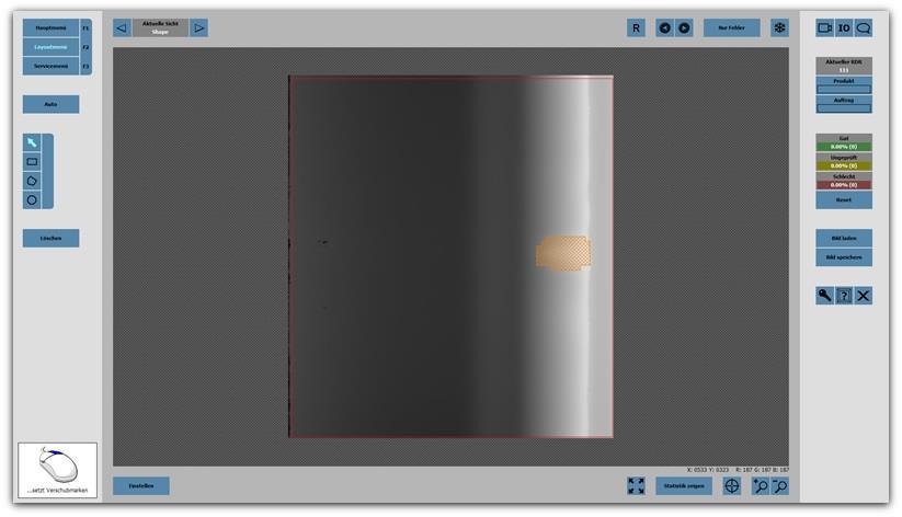
7 State of the Art: Integration in Line Surface Inspection Print Inspection Can Top Inspection Inspection directly in line saves money, a defective vessel will not pass following processing steps. But: In the following processing steps a new defect can arise, that will not be detected anymore, because it occurs behind the inspection units.

 CTI (Can Top Inspection) Patent granted DE 10")
8 State of the Art: Integration in Line Inspection of print directly behind the printer Inspection of curl & shoulder directly in tool plate of necking machine illumination camera PI (Print Inspection) CTI (Can Top Inspection) Patent granted DE

9 State of the Art: Integration in Line Patent granted DE CTI (Can Top Inspection) OK Top view: all information in one image Backside of curl and hidden shoulder is visible! Picture by courtesy of Ball, Velim CZ

10 State of the Art: Integration in Line CTI (Can Top Inspection) Detection of hidden defects One camera system in necker tool-plate with additional optic
11 New: Inspection at End of Line = Print Inspection + Can Top Inspection + Shape Control

12 New: Inspection at End of Line Can Inspection Machine: Can handler Inspection units First presentation of demonstrator at Metpack, Germany, May 2017

13 New: Inspection at End of Line Shape Control Can Inspection Machine Print Inspection Can Top Inspection


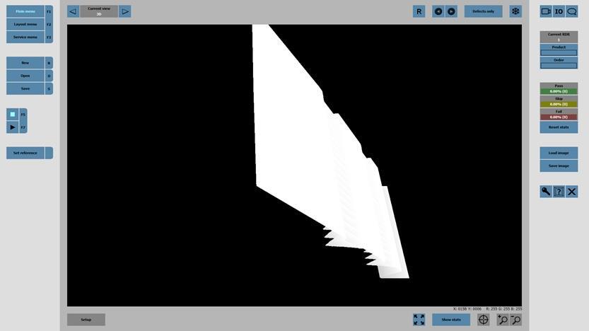
14 New: Inspection at End of Line World s fastest new 3D-camera implemented! Shape Control Can Inspection Machine Print Inspection Can Top Inspection 240 / min

15 3D-Measurement (Laser triangulation)

16 Images from laser line are 30 khz and are put together Overexposed for demonstration The thinner the line the better the measurement

17 Sensor Because of Si-based chips detectors have their highest response in red and IR-range. Red laser line produces good response on chip. But line width is too large.

18 2017/08/23 Laser line bpp=m 2 l Gaussian shape, diffraction limited Deep blue has the thinnest line in VIS Also speckles are reduced (diameter speckle prop. to l) (If roughness of the surface is in the range of the wavelength speckles) Fiber-coupled diode laser with 10 µm (width) blue line Straylight can be filtered out by use of bandpass-filter, just the laser-wavelength is transmitted beam parameter product M 2 beam quality factor l wavelength Speckles

19 Blue laser with M Fiber-coupled laser Micro focus line Class 2M ( safe, no housing necessary)
20 Need of thin laser line blue laser (450 nm) Camera has to be more sensitive

21 capabilities/aerosol/1-piece-aluminum-shaped 30 mm khz 16 subpixel levels 3200 height levels 45 mm e.g. 30 mm 45 mm Diameter Max. Resolution = 7.5 mm / 3200 = 2 µm
22 Laser 3D-Camera Overexposed and slow motion for demonstration Can The principle:
23 Laser 3D-Camera Overexposed and slow motion for demonstration Can The principle:
24 Laser 3D-Camera Overexposed and slow motion for demonstration Can The principle:
25 Laser 3D-Camera Overexposed and slow motion for demonstration Can The principle:
26 Laser 3D-Camera Overexposed and slow motion for demonstration Can The principle:
27 Laser 3D-Camera Overexposed and slow motion for demonstration Can The principle:
28 Laser 3D-Camera Overexposed and slow motion for demonstration Can The principle:
29 Laser 3D-Camera Overexposed and slow motion for demonstration Can The principle:
30 Laser 3D-Camera Overexposed and slow motion for demonstration Can The principle:

31 Laser 3D-Camera Overexposed and slow motion for demonstration Can The principle:
32 Laser 3D-Camera Overexposed and slow motion for demonstration Can The principle:
33 Laser 3D-Camera Overexposed and slow motion for demonstration Can The principle:
34 Laser 3D-Camera Overexposed and slow motion for demonstration Can The principle:
35 Laser 3D-Camera Overexposed and slow motion for demonstration Can The principle:
36 Laser 3D-Camera Overexposed and slow motion for demonstration Can The principle:
37 Laser 3D-Camera Overexposed and slow motion for demonstration Can The principle:
38 Laser 3D-Camera Overexposed and slow motion for demonstration Can The principle:
39
40
41
42
43
44
45
46
47
48
49
50
51
52
53
54
55
56
57
58
59
60
61
62
63
64
65
66
67
68
69
70
71
72
73
74
75
76
77
78
79
80
81
82
83
84
85


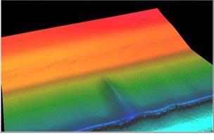
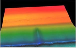
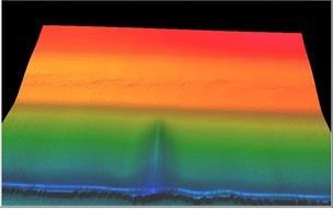
86 Curl Wrinkle Dent Shape grayvalue ~ height information about depth of defects is available
87 Software
88
 few 10")
89 Surface Inspection Software Shape Control Inspection of height Resolution (height) few 10 µm (!)
90 Summary Inspection at End of Line: Print Inspection Can Top Inspection Shape Control Even smallest defects can be detected in the surface in the range of few ten micrometer Of course fully automatized!

91 Thank you for your attention
attocfm I for Surface Quality Inspection NANOSCOPY APPLICATION NOTE M01 RELATED PRODUCTS G
 APPLICATION NOTE M01 attocfm I for Surface Quality Inspection Confocal microscopes work by scanning a tiny light spot on a sample and by measuring the scattered light in the illuminated volume. First,
Z-LASER Optoelektronik GmbH Stemmer 3d Technologietag Useful information on Z-Lasers for Vision
 Z-LASER Optoelektronik GmbH Stemmer 3d Technologietag - 24.2.2011 Useful information on Z-Lasers for Vision The Company Core Competences How to Build a Z-LASER Electronics and Modulation Wavelength and
PGS Family Plane Grating Spectrometer from ZEISS
 PGS Family Plane Grating Spectrometer from ZEISS 2 PGS Family the NIR specialists The spectrometers of the PGS family are designed for use in the NIR. InGaAs (indium-galliumarsenide) is used as a detector
Distance Sensors BOD 26K.... with optional Master-Slave-Mode
 Distance... with optional Master-Slave-Mode Laser Distance The Balluff distance sensor not only detects the presence of objects, but can also indicate their precise position or location. This means the
ColorRanger E 3D Cameras. Explore the true colors of Ranger MultiScan. PDF processed with CutePDF evaluation edition
 P r o d u c t I n f o r m at i o n ColorRanger E D Cameras Explore the true colors of Ranger MultiScan PDF processed with CutePDF evaluation edition www.cutepdf.com ColorRanger E: High-speed D and color
Titelfoto. Advanced Laser Beam Shaping - for Optimized Process Results and Quality Inspection in the PV Production - Maja Thies.
 2010 LIMO Lissotschenko Mikrooptik GmbH www.limo.de Titelfoto Advanced Laser Beam Shaping - for Optimized Process Results and Quality Inspection in the PV Production - Maja Thies Photonics Key Technology
NELA Brüder Neumeister GmbH
 Vision Inspection Systems NELA Brüder Neumeister GmbH Your Worldwide Partner for Automatic Optical Inspection and Sorting Systems see. control. automate. HISTORICAL MILESTONES 1938 Ernst and Bernhard Neumeister
Design Description Document
 UNIVERSITY OF ROCHESTER Design Description Document Flat Output Backlit Strobe Dare Bodington, Changchen Chen, Nick Cirucci Customer: Engineers: Advisor committee: Sydor Instruments Dare Bodington, Changchen
The Importance of Wavelengths on Optical Designs
 1 The Importance of Wavelengths on Optical Designs Bad Kreuznach, Oct. 2017 2 Introduction A lens typically needs to be corrected for many different parameters as e.g. distortion, astigmatism, spherical
M70LL Laser Distance Sensor
 M7LL Laser Distance Sensor for automated manufacturing with Ethernet interface to connect with PLC The analog sensors of series M7LL use a PSD for their receiver optics. This assures a position measurement
Practical Applications of Laser Technology for Semiconductor Electronics
 Practical Applications of Laser Technology for Semiconductor Electronics MOPA Single Pass Nanosecond Laser Applications for Semiconductor / Solar / MEMS & General Manufacturing Mark Brodsky US Application
Real-time Laser Beam Position Detector. XY-4QD User Manual
 Real-time Laser Beam Position Detector XY4QD User Manual page 1 of 7 1. Introduction The XY4QD is a 4-quadrant-diode with readout electronics and outputs for x and y position. The position of the laser
Optical Characterization and Defect Inspection for 3D Stacked IC Technology
 Minapad 2014, May 21 22th, Grenoble; France Optical Characterization and Defect Inspection for 3D Stacked IC Technology J.Ph.Piel, G.Fresquet, S.Perrot, Y.Randle, D.Lebellego, S.Petitgrand, G.Ribette FOGALE
Basic methods in imaging of micro and nano structures with atomic force microscopy (AFM)
") Basic methods in imaging of micro and nano P2538000 AFM Theory The basic principle of AFM is very simple. The AFM detects the force interaction between a sample and a very tiny tip (
Basic methods in imaging of micro and nano P2538000 AFM Theory The basic principle of AFM is very simple. The AFM detects the force interaction between a sample and a very tiny tip (
Evaluation of laser-based active thermography for the inspection of optoelectronic devices
 More info about this article: http://www.ndt.net/?id=15849 Evaluation of laser-based active thermography for the inspection of optoelectronic devices by E. Kollorz, M. Boehnel, S. Mohr, W. Holub, U. Hassler
Design of Sub-Wavelength Color Filters Design and Simulation with the RSoft Tools Synopsys, Inc. 1
 Design of Sub-Wavelength Color Filters Design and Simulation with the RSoft Tools 2018 Synopsys, Inc. 1 Outline Introduction Plasmonic color filters Dielectric color filters Related Topics Conclusion 2018
EXPERIMENTAL OBSERVATIONS OF THE LASER KEYHOLE WELDING PROCESS OF AA
 EXPERIMENTAL OBSERVATIONS OF THE LASER KEYHOLE WELDING PROCESS OF AA5182 1801 B.J. Aalderink 1, R.G.K.M. Aarts 2, J.B. Jonker 2 and J. Meijer 2 1 Netherlands Institute for Metals Research P.O. Box 217,
Using Stock Optics. ECE 5616 Curtis
 Using Stock Optics What shape to use X & Y parameters Please use achromatics Please use camera lens Please use 4F imaging systems Others things Data link Stock Optics Some comments Advantages Time and
Parallel Mode Confocal System for Wafer Bump Inspection
 Parallel Mode Confocal System for Wafer Bump Inspection ECEN5616 Class Project 1 Gao Wenliang wen-liang_gao@agilent.com 1. Introduction In this paper, A parallel-mode High-speed Line-scanning confocal
Wire bond inspection. Systems for the reliable inspection of wire bond connections in electronics manufacturing 3D SPI 3D AXI 3D MXI 3D AOI
 Wire bond inspection 3D SPI 3D AOI 3D AXI 3D MXI Systems for the reliable inspection of wire bond connections in electronics manufacturing Bent wires Missing wire on wedge Bond connections reliably inspected
Features. Applications. Optional Features
 Features Compact, Rugged Design TEM Beam with M 2 < 1.2 Pulse Rates from Single Shot to 15 khz IR, Green, UV, and Deep UV Wavelengths Available RS232 Computer Control Patented Harmonic Generation Technology
Silicon wafer thickness monitor
 Silicon wafer thickness monitor SIT-200 Alnair Labs Corporation 2016.04.20 Principle of Measurement Silicon wafer Optical fiber Sensor head Wavelength tunable laser PD PD Interference signal Power monitor
Sensors & Applications Glass Industry. More Precision
 Sensors & Applications Glass Industry More Precision Sensors and measuring systems for glass production Modern glass production is increasingly determined by maximum efficiency. Therefore, rapid access
New Aspects of Coin Measurement in Quality Inspection
 New Aspects of Coin Measurement in Quality Inspection Dr. Ralf Freiberger Technical Forum Berlin 2018 Ralf Freiberger 2 Overview 1. Purpose 2. Determination of dimensions 3. 4. Summary and outlook 3 Purpose
Sensitive measurement of partial coherence using a pinhole array
 1.3 Sensitive measurement of partial coherence using a pinhole array Paul Petruck 1, Rainer Riesenberg 1, Richard Kowarschik 2 1 Institute of Photonic Technology, Albert-Einstein-Strasse 9, 07747 Jena,
A-CUBE-Series High Sensitivity APD Detector Modules
 Series Description Laser Components new A-CUBE range of APD modules has been designed for customers interested in experimenting with APDs. Featuring a low-noise silicon (or InGaAs) APD with matched preamplifier
Variable microinspection system. system125
 Variable microinspection system system125 Variable micro-inspection system Characteristics Large fields, high NA The variable microinspection system mag.x system125 stands out from conventional LD inspection
attosnom I: Topography and Force Images NANOSCOPY APPLICATION NOTE M06 RELATED PRODUCTS G
 APPLICATION NOTE M06 attosnom I: Topography and Force Images Scanning near-field optical microscopy is the outstanding technique to simultaneously measure the topography and the optical contrast of a sample.
Infinitely Precise. micrometal. excellence in etching
 Infinitely Precise micrometal excellence in etching A High-Tech Profile Superfine structures and ultra-tight tolerances: precision is our business You give us the specs, and we etch to ultra-tight tolerances.
Optotop. 3D Topography. Roughness (Ra opt, Rq opt, and Rz opt) Height Distribution. Porosity Distribution. Effective Contact Area
 Height Distribution. Porosity Distribution. Effective Contact Area") Optotop 3D Topography Roughness (Ra opt, Rq opt, and Rz opt) Height Distribution Porosity Distribution Effective Contact Area Basic Functions Highlights Big measurement area up to 60mm x 60mm Easy operation
Optotop 3D Topography Roughness (Ra opt, Rq opt, and Rz opt) Height Distribution Porosity Distribution Effective Contact Area Basic Functions Highlights Big measurement area up to 60mm x 60mm Easy operation
- Near Field Scanning Optical Microscopy - Electrostatic Force Microscopy - Magnetic Force Microscopy
 - Near Field Scanning Optical Microscopy - Electrostatic Force Microscopy - Magnetic Force Microscopy Yongho Seo Near-field Photonics Group Leader Wonho Jhe Director School of Physics and Center for Near-field
LASER. Analog Laser Displacement Transducer. LAS Series. Key-Features:
 LASER Analog Laser Displacement Transducer LAS Series Key-Features: Content: Measurement Principle & Installation...2 Overview of the Series...3 Technical Data.4 Technical Drawing...7 Linearity & Resolution...8
TechNote. T001 // Precise non-contact displacement sensors. Introduction
 TechNote T001 // Precise non-contact displacement sensors Contents: Introduction Inductive sensors based on eddy currents Capacitive sensors Laser triangulation sensors Confocal sensors Comparison of all
Growing a NASA Sponsored Metrology Project to Serve Many Applications and Industries. James Millerd President, 4D Technology
 Growing a NASA Sponsored Metrology Project to Serve Many Applications and Industries James Millerd President, 4D Technology Outline In the Beginning Early Technology The NASA Connection NASA Programs First
Acuity. Acuity. AP620 Profile Measurement Scanner. Principles of Operation. Definitions. Typical Scanner Applications
 The AP620 profile measurement scanner is s short-range laser scanner for industrial contour and shape measuring applications. The laser profile scanner quickly and accurately generates 2D or 3D profile
Speckle Mitigation in Laser-Based Projectors
 Speckle Mitigation in Laser-Based Projectors Fergal Shevlin, Ph.D. CTO, Dyoptyka. Laser Display Conference, Yokohama, Japan, 2012/04/26-27. What does speckle look like? Can speckle be reduced? How can
Optical basics for machine vision systems. Lars Fermum Chief instructor STEMMER IMAGING GmbH
 Optical basics for machine vision systems Lars Fermum Chief instructor STEMMER IMAGING GmbH www.stemmer-imaging.de AN INTERNATIONAL CONCEPT STEMMER IMAGING customers in UK Germany France Switzerland Sweden
Properties of Structured Light
 Properties of Structured Light Gaussian Beams Structured light sources using lasers as the illumination source are governed by theories of Gaussian beams. Unlike incoherent sources, coherent laser sources
Radial Polarization Converter With LC Driver USER MANUAL
 ARCoptix Radial Polarization Converter With LC Driver USER MANUAL Arcoptix S.A Ch. Trois-portes 18 2000 Neuchâtel Switzerland Mail: info@arcoptix.com Tel: ++41 32 731 04 66 Principle of the radial polarization
The spectral colours of nanometers
 Reprint from the journal Mikroproduktion 3/2005 Berthold Michelt and Jochen Schulze The spectral colours of nanometers Precitec Optronik GmbH Raiffeisenstraße 5 D-63110 Rodgau Phone: +49 (0) 6106 8290-14
Automatic optical measurement of high density fiber connector
 Key Engineering Materials Online: 2014-08-11 ISSN: 1662-9795, Vol. 625, pp 305-309 doi:10.4028/www.scientific.net/kem.625.305 2015 Trans Tech Publications, Switzerland Automatic optical measurement of
Amplified Photodetectors
 Amplified Photodetectors User Guide (800)697-6782 sales@eotech.com www.eotech.com Page 1 of 6 EOT AMPLIFIED PHOTODETECTOR USER S GUIDE Thank you for purchasing your Amplified Photodetector from EOT. This
INTRODUCTION 提夫自控技术 ( 上海 ) 有限公司 LAS laser sensors cover measurement ranges from 1 to mm. The integrated micro-controller delivers an accur
 有限公司 LAS laser sensors cover measurement ranges from 1 to mm. The integrated micro-controller delivers an accur") LASER Analog Laser Displacement Transducer LAS Series Key-Features: Content: Measurement Principle & Installation...2 Overview of the Series...3 Technical Data.4 Technical Drawings...9 Diagrams...10 Order
LASER Analog Laser Displacement Transducer LAS Series Key-Features: Content: Measurement Principle & Installation...2 Overview of the Series...3 Technical Data.4 Technical Drawings...9 Diagrams...10 Order
Chapter 17: Wave Optics. What is Light? The Models of Light 1/11/13
 Chapter 17: Wave Optics Key Terms Wave model Ray model Diffraction Refraction Fringe spacing Diffraction grating Thin-film interference What is Light? Light is the chameleon of the physical world. Under
Lithography. 3 rd. lecture: introduction. Prof. Yosi Shacham-Diamand. Fall 2004
 Lithography 3 rd lecture: introduction Prof. Yosi Shacham-Diamand Fall 2004 1 List of content Fundamental principles Characteristics parameters Exposure systems 2 Fundamental principles Aerial Image Exposure
Inline PL Imaging Techniques for Crystalline Silicon Cell Production. F. Korsós, Z. Kiss, Ch. Defranoux and S. Gaillard
 Inline PL Imaging Techniques for Crystalline Silicon Cell Production F. Korsós, Z. Kiss, Ch. Defranoux and S. Gaillard OUTLINE I. Categorization of PL imaging techniques II. PL imaging setups III. Inline
Tapered Amplifiers. For Amplification of Seed Sources or for External Cavity Laser Setups. 750 nm to 1070 nm COHERENT.COM DILAS.
 Tapered Amplifiers For Amplification of Seed Sources or for External Cavity Laser Setups 750 nm to 1070 nm COHERENT.COM DILAS.COM Welcome DILAS Semiconductor is now part of Coherent Inc. With operations
FLEXPOINT Machine Vision Lasers MVfemto Series (Edition 2017)
") FLEXPOINT Machine Vision s Smallest Machine Vision on the Market With the MVfemto line laser, LASER COMPONENTS presents the smallest machine vision laser with outstanding optical performance. With dimensions
FLEXPOINT Machine Vision s Smallest Machine Vision on the Market With the MVfemto line laser, LASER COMPONENTS presents the smallest machine vision laser with outstanding optical performance. With dimensions
Laser Telemetric System (Metrology)
") Laser Telemetric System (Metrology) Laser telemetric system is a non-contact gauge that measures with a collimated laser beam (Refer Fig. 10.26). It measure at the rate of 150 scans per second. It basically
Laser Telemetric System (Metrology) Laser telemetric system is a non-contact gauge that measures with a collimated laser beam (Refer Fig. 10.26). It measure at the rate of 150 scans per second. It basically
Hermetic Packaging Solutions using Borosilicate Glass Thin Films. Lithoglas Hermetic Packaging Solutions using Borosilicate Glass Thin Films
 Hermetic Packaging Solutions using Borosilicate Glass Thin Films 1 Company Profile Company founded in 2006 ISO 9001:2008 qualified since 2011 Headquarters and Production in Dresden, Germany Production
PICO MASTER 200. UV direct laser writer for maskless lithography
 PICO MASTER 200 UV direct laser writer for maskless lithography 4PICO B.V. Jan Tinbergenstraat 4b 5491 DC Sint-Oedenrode The Netherlands Tel: +31 413 490708 WWW.4PICO.NL 1. Introduction The PicoMaster
EE119 Introduction to Optical Engineering Spring 2003 Final Exam. Name:
 EE119 Introduction to Optical Engineering Spring 2003 Final Exam Name: SID: CLOSED BOOK. THREE 8 1/2 X 11 SHEETS OF NOTES, AND SCIENTIFIC POCKET CALCULATOR PERMITTED. TIME ALLOTTED: 180 MINUTES Fundamental
NON-AMPLIFIED HIGH SPEED PHOTODETECTOR USER S GUIDE
 NON-AMPLIFIED HIGH SPEED PHOTODETECTOR USER S GUIDE Thank you for purchasing your Non-amplified High Speed Photodetector. This user s guide will help answer any questions you may have regarding the safe
X-SCOPE Ultra large FOV micro video colorimeter
 To obtain more information on any of the products below go to our new newsletter page on the website and follow the links, send an email to sales@alrad.co.uk or call 01635 30345. As this is our last newsletter
Optical Components for Laser Applications. Günter Toesko - Laserseminar BLZ im Dezember
 Günter Toesko - Laserseminar BLZ im Dezember 2009 1 Aberrations An optical aberration is a distortion in the image formed by an optical system compared to the original. It can arise for a number of reasons
From the start the main activity of our company was the development and production of infrared illuminators.
 catalogue 2010 INFRA - RED ILLUMINATION The Tirex company, producer of the ELENEK illuminators, was founded in 1992 by specialists of the Physical and Technical Institute of Saint-Petersburg From the start
PowerMax-Pro Sensors. 100 mw to 150W FEATURES
 PowerMax-Pro Sensors PowerMax-Pro (Patent #9,012,848) represents a dramatic technological advancement in laser power sensing that combines the broad wavelength sensitivity, dynamic range and laser damage
NON-AMPLIFIED PHOTODETECTOR USER S GUIDE
 NON-AMPLIFIED PHOTODETECTOR USER S GUIDE Thank you for purchasing your Non-amplified Photodetector. This user s guide will help answer any questions you may have regarding the safe use and optimal operation
Vixar High Power Array Technology
 Vixar High Power Array Technology I. Introduction VCSELs arrays emitting power ranging from 50mW to 10W have emerged as an important technology for applications within the consumer, industrial, automotive
FLEXPOINT Machine Vision Lasers MVmicro Series
 FLEXPOINT Machine Vision Lasers MVmicro Series The FLEXPOINT MVmicro series was developed for stand alone machine vision applications, primarily in use together with industrial cameras in 3D measuements.
HIGH SPEED FIBER PHOTODETECTOR USER S GUIDE
 HIGH SPEED FIBER PHOTODETECTOR USER S GUIDE Thank you for purchasing your High Speed Fiber Photodetector. This user s guide will help answer any questions you may have regarding the safe use and optimal
Optical Microscopy and Imaging ( Part 2 )
") 1 Optical Microscopy and Imaging ( Part 2 ) Chapter 7.1 : Semiconductor Science by Tudor E. Jenkins Saroj Kumar Patra, Department of Electronics and Telecommunication, Norwegian University of Science and
1 Optical Microscopy and Imaging ( Part 2 ) Chapter 7.1 : Semiconductor Science by Tudor E. Jenkins Saroj Kumar Patra, Department of Electronics and Telecommunication, Norwegian University of Science and
COMPACT Diode Laser System (Water-Cooled)
") COMPACT Diode Laser System (Water-Cooled) Easy-to-integrate CW system consists of a compact 19 (11HU including water-air-chiller), rack-mountable chassis and metal-armored fiber. Can be combined with DILAS
COMPACT Diode Laser System (Water-Cooled) Easy-to-integrate CW system consists of a compact 19 (11HU including water-air-chiller), rack-mountable chassis and metal-armored fiber. Can be combined with DILAS
Laser tests of Wide Band Gap power devices. Using Two photon absorption process
 Laser tests of Wide Band Gap power devices Using Two photon absorption process Frederic Darracq Associate professor IMS, CNRS UMR5218, Université Bordeaux, 33405 Talence, France 1 Outline Two-Photon absorption
Moving from biomedical to industrial applications: OCT Enables Hi-Res ND Depth Analysis
 Moving from biomedical to industrial applications: OCT Enables Hi-Res ND Depth Analysis Patrick Merken a,c, Hervé Copin a, Gunay Yurtsever b, Bob Grietens a a Xenics NV, Leuven, Belgium b UGENT, Ghent,
SUPRA Optix 3D Optical Profiler
 SUPRA Optix 3D Optical Profiler Scanning White-light Interferometric Microscope SWIM Series Applications The SUPRA Optix is the latest development in the field of Scanning White-light Interferometry. With
Integrating Spheres. Why an Integrating Sphere? High Reflectance. How Do Integrating Spheres Work? High Damage Threshold
 1354 MINIS Oriel Integrating Spheres Integrating spheres are ideal optical diffusers; they are used for radiometric measurements where uniform illumination or angular collection is essential, for reflectance
AG Optical Systems. Newtonian Astrograph Manual Version AG Optical Systems
 AG Optical Systems Newtonian Astrograph Manual Version 2 2012 Table of Contents 1. Introduction 2. System Specifications 3. Initial Assembly 4. Collimation 5. Care and Cleaning 6. Cooling Fan Operation
You have a task. We have a solution. flo-ir berührungslos messen
 flo-ir berührungslos messen Aawasserstrasse 10 CH 6370 Oberdorf, NW Tel.: +41 (0)41 871 39 88 Fax: +41 (0)41 871 39 87 info@flo-ir.ch www.flo-ir.ch You have a task We have a solution - 2 - What can be
Integrated Diode Laser System DioPower
 Integrated Diode Laser System DioPower PC with LETSoft program DioPower Integrated Components Applications Laser Diode from 15 to 120W Material processing Laser Diode driver up to 6V / 100A Laser soldering
The End of Thresholds: Subwavelength Optical Linewidth Measurement Using the Flux-Area Technique
 The End of Thresholds: Subwavelength Optical Linewidth Measurement Using the Flux-Area Technique Peter Fiekowsky Automated Visual Inspection, Los Altos, California ABSTRACT The patented Flux-Area technique
Laser Speckle Reducer LSR-3000 Series
 Datasheet: LSR-3000 Series Update: 06.08.2012 Copyright 2012 Optotune Laser Speckle Reducer LSR-3000 Series Speckle noise from a laser-based system is reduced by dynamically diffusing the laser beam. A
High-speed Micro-crack Detection of Solar Wafers with Variable Thickness
 High-speed Micro-crack Detection of Solar Wafers with Variable Thickness T. W. Teo, Z. Mahdavipour, M. Z. Abdullah School of Electrical and Electronic Engineering Engineering Campus Universiti Sains Malaysia
Adaptive Optics for LIGO
 Adaptive Optics for LIGO Justin Mansell Ginzton Laboratory LIGO-G990022-39-M Motivation Wavefront Sensor Outline Characterization Enhancements Modeling Projections Adaptive Optics Results Effects of Thermal
Xenon-Zirconia 3.3/92
 This lens with.2x magnification is optimized for the use with 12k (62.5 mm) line scan sensors with 5 µm pixel, but can also be used with 16k (82 mm) lines. It is broadband coated and can be used in the
REAL TIME THICKNESS MEASUREMENT OF A MOVING WIRE
 REAL TIME THICKNESS MEASUREMENT OF A MOVING WIRE Bini Babu 1, Dr. Ashok Kumar T 2 1 Optoelectronics and communication systems, 2 Associate Professor Model Engineering college, Thrikkakara, Ernakulam, (India)
Advanced Optical Inspection Techniques
 Advanced Optical Inspection Techniques September 9, 2010 Andrei Brunfeld Contents Introduction Current Challenges Areal Density (Tb/in2) 4.000 3.500 3.000 2.500 2.000 1.500 1.000 0.500 Areal Density and
Optics Laboratory Spring Semester 2017 University of Portland
 Optics Laboratory Spring Semester 2017 University of Portland Laser Safety Warning: The HeNe laser can cause permanent damage to your vision. Never look directly into the laser tube or at a reflection
THICKNESS CHECK NON-CONTACT THICKNESS MEASUREMENT OF FLAT PRODUCTS
 EN THICKNESS CHECK NON-CONTACT THICKNESS MEASUREMENT OF FLAT PRODUCTS CALIX NON-CONTACT INLINE THICKNESS MEASUREMENT MEASURING RANGE STRIP THICKNESS EDGE THICKNESS The CALIX series is a non-contact measuring
Chemistry Instrumental Analysis Lecture 10. Chem 4631
 Chemistry 4631 Instrumental Analysis Lecture 10 Types of Instrumentation Single beam Double beam in space Double beam in time Multichannel Speciality Types of Instrumentation Single beam Requires stable
Coaxial Lights LFV3 series
 Refer to our website for product details. CCS Use a search engine. Search You can also use your smartphone or cell phone. Provides diffused light evenly from the same axis as the camera -SW -SW -CP-18SW
Effect of Beam Size on Photodiode Saturation
 Effect of Beam Size on Photodiode Saturation Experiments were conducted to demonstrate a change in the saturation point for a FDS1010 silicon photodiode as a function of beam diameter. The saturation point
MEASUREMENT APPLICATION GUIDE OUTER/INNER
 MEASUREMENT APPLICATION GUIDE OUTER/INNER DIAMETER Measurement I N D E X y Selection Guide P.2 y Measurement Principle P.3 y P.4 y X and Y Axes Synchronous Outer Diameter Measurement P.5 y of a Large Diameter
Nanoimprint lithography with a focused laser beam for the fabrication of micro-/nano-hybrid patterns
 Supplementary Material (ESI) for Lab on a Chip This journal is The Royal Society of Chemistry 20XX Nanoimprint lithography with a focused laser beam for the fabrication of micro-/nano-hybrid patterns Hyungjun
Research Grade Xenon Arc Lamp Sources LH-Series 75 W - 300W
 Research Grade Xenon Arc Lamp Sources LH-Series 75 W - 300W Features Vertical or horizontal bulb and housing operation Xenon arc lamps from 75W to 300W Multiple collimated or focused output optics in various
A Breakthrough in Sputtering Target Inspections: Ultra-High Speed Phased Array Scanning with Volume Focusing
 17th World Conference on Nondestructive Testing, 25-28 Oct 2008, Shanghai, China A Breakthrough in Sputtering Target Inspections: Ultra-High Speed Phased Array Scanning with Volume Focusing Dominique Braconnier,
Photonic device package design, assembly and encapsulation.
 Photonic device package design, assembly and encapsulation. Abstract. A.Bos, E. Boschman Advanced Packaging Center. Duiven, The Netherlands Photonic devices like Optical transceivers, Solar cells, LED
Measuring intensity in watts rather than lumens
 Specialist Article Appeared in: Markt & Technik Issue: 43 / 2013 Measuring intensity in watts rather than lumens Authors: David Schreiber, Developer Lighting and Claudius Piske, Development Engineer Hardware
Macro Varon 4.5/85. Key features. Applications. Web and surface inspections
 The Macro Varon lens has been designed for high resolution 12k line scan cameras with 3.5 µm pixel pitch. They are optimized for an optical magnification range of.5x to 2.x. CAS-lens technology produces
Laser diffuse reflection light scanner with background suppression. Dimensioned drawing
 Specifications and description Laser diffuse reflection light scanner with background suppression Dimensioned drawing We reserve the right to make changes DS_HRTL3B_en.fm en 01-2010/12 50114049 10-30 V
INTERFEROMETER VI-direct
 Universal Interferometers for Quality Control Ideal for Production and Quality Control INTERFEROMETER VI-direct Typical Applications Interferometers are an indispensable measurement tool for optical production
CCDs for Earth Observation James Endicott 1 st September th UK China Workshop on Space Science and Technology, Milton Keynes, UK
 CCDs for Earth Observation James Endicott 1 st September 2011 7 th UK China Workshop on Space Science and Technology, Milton Keynes, UK Introduction What is this talk all about? e2v sensors in spectrometers
Okamoto Machine Tool Works, LTD. June 22, th SEMATECH Symposium Japan 1
 Okamoto Machine Tool Works, LTD 1 Contents Solutions for TSV Wafer Thinning Process (Front Side Via) TSV Wafer Thinning Challenges Process Improvement (4-years Development) TSV Wafer Thinning Tool (TSV300)
Difrotec Product & Services. Ultra high accuracy interferometry & custom optical solutions
 Difrotec Product & Services Ultra high accuracy interferometry & custom optical solutions Content 1. Overview 2. Interferometer D7 3. Benefits 4. Measurements 5. Specifications 6. Applications 7. Cases
REAL TIME SURFACE DEFORMATIONS MONITORING DURING LASER PROCESSING
 The 8 th International Conference of the Slovenian Society for Non-Destructive Testing»Application of Contemporary Non-Destructive Testing in Engineering«September 1-3, 2005, Portorož, Slovenia, pp. 335-339
Micromachining with tailored Nanosecond Pulses
 Micromachining with tailored Nanosecond Pulses Hans Herfurth a, Rahul Patwa a, Tim Lauterborn a, Stefan Heinemann a, Henrikki Pantsar b a )Fraunhofer USA, Center for Laser Technology (CLT), 46025 Port
COLOUR INSPECTION, INFRARED AND UV
 COLOUR INSPECTION, INFRARED AND UV TIPS, SPECIAL FEATURES, REQUIREMENTS LARS FERMUM, CHIEF INSTRUCTOR, STEMMER IMAGING THE PROPERTIES OF LIGHT Light is characterized by specifying the wavelength, amplitude
Hybrid Surface Contour Measuring Machine FORMTRACER CS-5000
 Form Measurement Hybrid Surface Contour Measuring Machine FORMTRCER CS-5000 CTLOG No. E4220-525 hybrid surface contour measuring machine that combines contour and surface roughness measurements and analyses
Improving the Collection Efficiency of Raman Scattering
 PERFORMANCE Unparalleled signal-to-noise ratio with diffraction-limited spectral and imaging resolution Deep-cooled CCD with excelon sensor technology Aberration-free optical design for uniform high resolution
Optical Requirements
 Optical Requirements Transmission vs. Film Thickness A pellicle needs a good light transmission and long term transmission stability. Transmission depends on the film thickness, film material and any anti-reflective