Metal Oxide Semiconductor Field-Effect Transistors (MOSFETs)
|
|
|
- Ethelbert Parrish
- 5 years ago
- Views:
Transcription
1 Metal Oxide Semiconductor Field-Effect Transistors (MOSFETs)

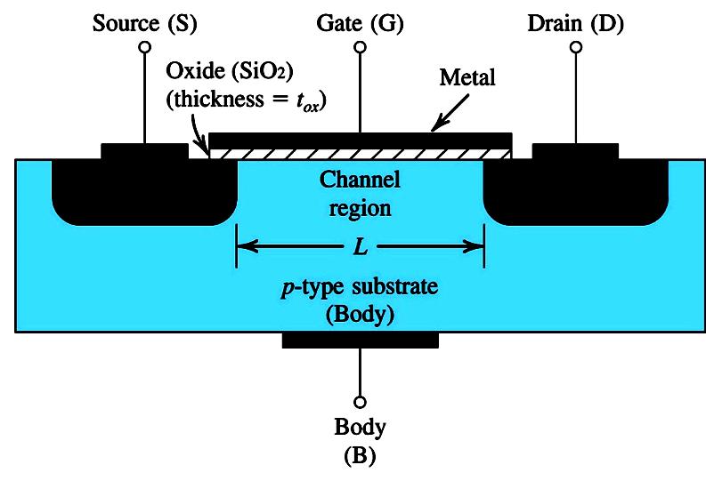
2 Device Structure

3 N-Channel MOSFET Providing electrons Pulling electrons (makes current flow) Apply positive voltage to gate: Drives away holes and attracts electrons in the body under gate Creates an n-channel between the source and drain and now current can flow Electronic Devices: Field Effect Transistors

4 Operation with Zero Gate Voltage Two back-to-back diodes, High Resistance (Giga Ohms), No Current Flow Microelectronic Circuits, Sixth Edition Sedra/Smith Copyright 2010 by Oxford University Press, Inc.
5 Creating a Channel for Current Flow -v GS :gate to source voltage -V t : threshold voltage (v GS which channel starts conducting) -i DS : current flowing when v DS applied -Effective voltage (or overdrive voltage): v GS V t v OV v eff Charge in the channel: Q = C ( WL) ox v OV -Oxide capacitance: ε ox Cox = tox -Gate to source capacitance: C = C WL ox

6 Applying a small v DS

7 Operation as v DS increases Channel becomes more tapered and its resistance increases
8 Saturation region (BJT) Active region (BJT) Microelectronic Circuits, Sixth Edition Sedra/Smith Copyright 2010 by Oxford University Press, Inc.
9 Operation for v DS >>V OV (channel pinch-off, saturation mode of operation) i v D OV ' n GS W ( ) v L V 1 ' W id = kn( 2 L k ' = µ C n 1 = k 2 = v n ox t 2 OV )( v GS V t ) 2 Microelectronic Circuits, Sixth Edition Sedra/Smith Copyright 2010 by Oxford University Press, Inc.

10 P-Channel MOSFET Microelectronic Circuits, Sixth Edition Sedra/Smith Copyright 2010 by Oxford University Press, Inc.
 Formulae are the same, switch sign of voltages Microelectronic Circuits, Sixth Edition Sedra/Smith Copyright 2010 by Oxford")
11 P-Channel MOSFET Threshold voltage v Use absolute value GS V tp vgs V tp P-Channel transistor process transconductance parameter k ' = µ C p p ox P-Channel transistor transconductance parameter k p = µ p C ox ( L W ) Formulae are the same, switch sign of voltages Microelectronic Circuits, Sixth Edition Sedra/Smith Copyright 2010 by Oxford University Press, Inc.

12 Complementary MOS or CMOS Figure 5.10 Cross-section of a CMOS integrated circuit. The PMOS transistor is formed in a separate n-type region (n well). Another arrangement is also possible in which an n-type body is used and the n device is formed in a p well. Not shown are the connections made to the p-type body and to the n well; the latter functions as the body terminal for the p-channel device. Microelectronic Circuits, Sixth Edition Sedra/Smith Copyright 2010 by Oxford University Press, Inc.
13 Current-Voltage Characteristics Figure 5.11 (a) Circuit symbol for the n-channel enhancement-type MOSFET. (b) Modified circuit symbol with an arrowhead on the source terminal to distinguish it from the drain and to indicate device polarity (i.e., n channel). (c) Simplified circuit symbol to be used when the source is connected to the body or when the effect of the body on device operation is unimportant.
14 Table 5.1 Regions of Operation of the Enhancement NMOS Transistor

15 Microelectronic Circuits, Sixth Edition Sedra/Smith Copyright 2010 by Oxford University Press, Inc. Stepping V GS
16 Microelectronic Circuits, Sixth Edition Sedra/Smith Copyright 2010 by Oxford University Press, Inc. The i D v GS Characteristic 2 ' 2 ' ) ( 2 1 ) )( ( 2 1 OV n D t GS n D v L W k i V v L W k i = = in term of v OV :

17 Large-signal equivalent-circuit model (DC) of an n- channel MOSFET operating in the saturation
18 Channel Length Effect i D = 2 W ( L 1 ' k )( ) 2 n vgs Vtn (1 + λv Channel-length modulation DS )
19 i D = 1 2 k ' n W ( L )( v GS V tn ) 2 1 r 0 = ==> r0 = λi D V I A D Microelectronic Circuits, Sixth Edition Sedra/Smith Copyright 2010 by Oxford University Press, Inc.

20 Large-signal equivalent circuit model r 0 = 1 λ I D
21 Characteristics of the p-channel MOSFET Figure 5.19 (a) Circuit symbol for the p-channel enhancement-type MOSFET. (b) Modified symbol with an arrowhead on the source lead. (c) Simplified circuit symbol for the case where the source is connected to the body.
22 Table 5.2 Regions of Operation of the Enhancement PMOS Transistor
23 Example MOSFET Circuits at DC Given: I D =0.4mA, V D =0.5V, V t =0.7V, µ n C ox =100 µa/v 2, L=1 µm, W=32 µm, λ=0 Find: R D, R S
24 Example 5.6 (p. 281)
25 Example 5.7 (p. 264) Given: I D =0.5mA V D =3V V tp =-1V PMOS Find: R G1 R G2
EE105 Fall 2015 Microelectronic Devices and Circuits: MOSFET Prof. Ming C. Wu 511 Sutardja Dai Hall (SDH)
") EE105 Fall 2015 Microelectronic Devices and Circuits: MOSFET Prof. Ming C. Wu wu@eecs.berkeley.edu 511 Sutardja Dai Hall (SDH) 7-1 Simplest Model of MOSFET (from EE16B) 7-2 CMOS Inverter 7-3 CMOS NAND
EE105 Fall 2015 Microelectronic Devices and Circuits: MOSFET Prof. Ming C. Wu wu@eecs.berkeley.edu 511 Sutardja Dai Hall (SDH) 7-1 Simplest Model of MOSFET (from EE16B) 7-2 CMOS Inverter 7-3 CMOS NAND
Introduction to MOSFET MOSFET (Metal Oxide Semiconductor Field Effect Transistor)
") Microelectronic Circuits Introduction to MOSFET MOSFET (Metal Oxide Semiconductor Field Effect Transistor) Slide 1 MOSFET Construction MOSFET (Metal Oxide Semiconductor Field Effect Transistor) Slide 2
Microelectronic Circuits Introduction to MOSFET MOSFET (Metal Oxide Semiconductor Field Effect Transistor) Slide 1 MOSFET Construction MOSFET (Metal Oxide Semiconductor Field Effect Transistor) Slide 2
ECEN325: Electronics Summer 2018
 ECEN325: Electronics Summer 2018 Metal-Oxide-Semiconductor Field Effect Transistor (MOSFET) Sam Palermo Analog & Mixed-Signal Center Texas A&M University Announcements & Reading H5 due today Exam 2 on
Lecture 16: MOS Transistor models: Linear models, SPICE models. Context. In the last lecture, we discussed the MOS transistor, and
 Lecture 16: MOS Transistor models: Linear models, SPICE models Context In the last lecture, we discussed the MOS transistor, and added a correction due to the changing depletion region, called the body
Field-Effect Transistor (FET) is one of the two major transistors; FET derives its name from its working mechanism;
 is one of the two major transistors; FET derives its name from its working mechanism;") Chapter 3 Field-Effect Transistors (FETs) 3.1 Introduction Field-Effect Transistor (FET) is one of the two major transistors; FET derives its name from its working mechanism; The concept has been known
Chapter 3 Field-Effect Transistors (FETs) 3.1 Introduction Field-Effect Transistor (FET) is one of the two major transistors; FET derives its name from its working mechanism; The concept has been known
Microelectronics Circuit Analysis and Design. MOS Capacitor Under Bias: Electric Field and Charge. Basic Structure of MOS Capacitor 9/25/2013
 Microelectronics Circuit Analysis and Design Donald A. Neamen Chapter 3 The Field Effect Transistor In this chapter, we will: Study and understand the operation and characteristics of the various types
55:041 Electronic Circuits
 55:041 Electronic Circuits Mosfet Review Sections of Chapter 3 &4 A. Kruger Mosfet Review, Page-1 Basic Structure of MOS Capacitor Sect. 3.1 Width 1 10-6 m or less Thickness 50 10-9 m or less ` MOS Metal-Oxide-Semiconductor
EEC 118 Spring 2010 Lab #1: NMOS and PMOS Transistor Parameters
 EEC 118 Spring 2010 Lab #1: NMOS and PMOS Transistor Parameters Dept. of Electrical and Computer Engineering University of California, Davis March 18, 2010 Reading: Rabaey Chapter 3 [1]. Reference: Kang
D n ox GS THN DS GS THN DS GS THN. D n ox GS THN DS GS THN DS GS THN
 Name: EXAM #3 Closed book, closed notes. Calculators may be used for numeric computations only. All work is to be your own - show your work for maximum partial credit. Data: Use the following data in all
Week 9a OUTLINE. MOSFET I D vs. V GS characteristic Circuit models for the MOSFET. Reading. resistive switch model small-signal model
 Week 9a OUTLINE MOSFET I vs. V GS characteristic Circuit models for the MOSFET resistive switch model small-signal model Reading Rabaey et al.: Chapter 3.3.2 Hambley: Chapter 12 (through 12.5); Section
Design cycle for MEMS
 Design cycle for MEMS Design cycle for ICs IC Process Selection nmos CMOS BiCMOS ECL for logic for I/O and driver circuit for critical high speed parts of the system The Real Estate of a Wafer MOS Transistor
UNIT-1 Bipolar Junction Transistors. Text Book:, Microelectronic Circuits 6 ed., by Sedra and Smith, Oxford Press
 UNIT-1 Bipolar Junction Transistors Text Book:, Microelectronic Circuits 6 ed., by Sedra and Smith, Oxford Press Figure 6.1 A simplified structure of the npn transistor. Microelectronic Circuits, Sixth
MOSFET Terminals. The voltage applied to the GATE terminal determines whether current can flow between the SOURCE & DRAIN terminals.
 MOSFET Terminals The voltage applied to the GATE terminal determines whether current can flow between the SOURCE & DRAIN terminals. For an n-channel MOSFET, the SOURCE is biased at a lower potential (often
EE 140 / EE 240A ANALOG INTEGRATED CIRCUITS FALL 2015 C. Nguyen PROBLEM SET #7
 Issued: Friday, Oct. 16, 2015 PROBLEM SET #7 Due (at 8 a.m.): Monday, Oct. 26, 2015, in the EE 140/240A HW box near 125 Cory. 1. A design error has resulted in a mismatch in the circuit of Fig. PS7-1.
Depletion-mode operation ( 공핍형 ): Using an input gate voltage to effectively decrease the channel size of an FET
: Using an input gate voltage to effectively decrease the channel size of an FET") Ch. 13 MOSFET Metal-Oxide-Semiconductor Field-Effect Transistor : I D D-mode E-mode V g The gate oxide is made of dielectric SiO 2 with e = 3.9 Depletion-mode operation ( 공핍형 ): Using an input gate voltage
Ch. 13 MOSFET Metal-Oxide-Semiconductor Field-Effect Transistor : I D D-mode E-mode V g The gate oxide is made of dielectric SiO 2 with e = 3.9 Depletion-mode operation ( 공핍형 ): Using an input gate voltage
Lecture 16. Complementary metal oxide semiconductor (CMOS) CMOS 1-1
 CMOS 1-1") Lecture 16 Complementary metal oxide semiconductor (CMOS) CMOS 1-1 Outline Complementary metal oxide semiconductor (CMOS) Inverting circuit Properties Operating points Propagation delay Power dissipation
Lecture 16 Complementary metal oxide semiconductor (CMOS) CMOS 1-1 Outline Complementary metal oxide semiconductor (CMOS) Inverting circuit Properties Operating points Propagation delay Power dissipation
MOS Field-Effect Transistors (MOSFETs)
") 6 MOS Field-Effect Transistors (MOSFETs) A three-terminal device that uses the voltages of the two terminals to control the current flowing in the third terminal. The basis for amplifier design. The basis
6 MOS Field-Effect Transistors (MOSFETs) A three-terminal device that uses the voltages of the two terminals to control the current flowing in the third terminal. The basis for amplifier design. The basis
Lecture 4. MOS transistor theory
 Lecture 4 MOS transistor theory 1.7 Introduction: A MOS transistor is a majority-carrier device, in which the current in a conducting channel between the source and the drain is modulated by a voltage
F9 Differential and Multistage Amplifiers
 Lars Ohlsson 018-10-0 F9 Differential and Multistage Amplifiers Outline MOS differential pair Common mode signal operation Differential mode signal operation Large signal operation Small signal operation
MOSFET & IC Basics - GATE Problems (Part - I)
") MOSFET & IC Basics - GATE Problems (Part - I) 1. Channel current is reduced on application of a more positive voltage to the GATE of the depletion mode n channel MOSFET. (True/False) [GATE 1994: 1 Mark]
MOSFET & IC Basics - GATE Problems (Part - I) 1. Channel current is reduced on application of a more positive voltage to the GATE of the depletion mode n channel MOSFET. (True/False) [GATE 1994: 1 Mark]
Microelectronics Circuit Analysis and Design
 Microelectronics Circuit Analysis and Design Donald A. Neamen Chapter 3 The Field Effect Transistor Neamen Microelectronics, 4e Chapter 3-1 In this chapter, we will: Study and understand the operation
EE5320: Analog IC Design
 EE5320: Analog IC Design Handout 3: MOSFETs Saurabh Saxena & Qadeer Khan Indian Institute of Technology Madras Copyright 2018 by EE6:Integrated Circuits & Systems roup @ IIT Madras Overview Transistors
INTRODUCTION: Basic operating principle of a MOSFET:
 INTRODUCTION: Along with the Junction Field Effect Transistor (JFET), there is another type of Field Effect Transistor available whose Gate input is electrically insulated from the main current carrying
4.5 Biasing in MOS Amplifier Circuits
 4.5 Biasing in MOS Amplifier Circuits Biasing: establishing an appropriate DC operating point for the MOSFET - A fundamental step in the design of a MOSFET amplifier circuit An appropriate DC operating
Field Effect Transistors
 Field Effect Transistors LECTURE NO. - 41 Field Effect Transistors www.mycsvtunotes.in JFET MOSFET CMOS Field Effect transistors - FETs First, why are we using still another transistor? BJTs had a small
Integrated Circuit Amplifiers. Comparison of MOSFETs and BJTs
 Integrated Circuit Amplifiers Comparison of MOSFETs and BJTs 17 Typical CMOS Device Parameters 0.8 µm 0.25 µm 0.13 µm Parameter NMOS PMOS NMOS PMOS NMOS PMOS t ox (nm) 15 15 6 6 2.7 2.7 C ox (ff/µm 2 )
Three Terminal Devices
 Three Terminal Devices - field effect transistor (FET) - bipolar junction transistor (BJT) - foundation on which modern electronics is built - active devices - devices described completely by considering
55:041 Electronic Circuits
 55:041 Electronic Circuits MOSFETs Sections of Chapter 3 &4 A. Kruger MOSFETs, Page-1 Basic Structure of MOS Capacitor Sect. 3.1 Width = 1 10-6 m or less Thickness = 50 10-9 m or less ` MOS Metal-Oxide-Semiconductor
Course Outline. 4. Chapter 5: MOS Field Effect Transistors (MOSFET) 5. Chapter 6: Bipolar Junction Transistors (BJT)
 5. Chapter 6: Bipolar Junction Transistors (BJT)") Course Outline 1. Chapter 1: Signals and Amplifiers 1 2. Chapter 3: Semiconductors 3. Chapter 4: Diodes 4. Chapter 5: MOS Field Effect Transistors (MOSFET) 5. Chapter 6: Bipolar Junction Transistors (BJT)
Course Outline 1. Chapter 1: Signals and Amplifiers 1 2. Chapter 3: Semiconductors 3. Chapter 4: Diodes 4. Chapter 5: MOS Field Effect Transistors (MOSFET) 5. Chapter 6: Bipolar Junction Transistors (BJT)
Electronic Circuits for Mechatronics ELCT 609 Lecture 6: MOS-FET Transistor
 Electronic Circuits for Mechatronics ELCT 609 Lecture 6: MOS-FET Transistor Assistant Professor Office: C3.315 E-mail: eman.azab@guc.edu.eg 1 Introduction Why we call it Transistor? The name came as an
Laboratory #5 BJT Basics and MOSFET Basics
 Laboratory #5 BJT Basics and MOSFET Basics I. Objectives 1. Understand the physical structure of BJTs and MOSFETs. 2. Learn to measure I-V characteristics of BJTs and MOSFETs. II. Components and Instruments
Part II: The MOS Transistor Technology. J. SÉE 2004/2005
 Part II: The MOS Transistor Technology J. SÉE johann.see@ief.u-psud.fr 2004/2005 Lecture plan Towards the nanotechnologies... data storage The data processing through the ages MOS transistor in logic-gates
COMPARISON OF THE MOSFET AND THE BJT:
 COMPARISON OF THE MOSFET AND THE BJT: In this section we present a comparison of the characteristics of the two major electronic devices: the MOSFET and the BJT. To facilitate this comparison, typical
MEASUREMENT AND INSTRUMENTATION STUDY NOTES UNIT-I
 MEASUREMENT AND INSTRUMENTATION STUDY NOTES The MOSFET The MOSFET Metal Oxide FET UNIT-I As well as the Junction Field Effect Transistor (JFET), there is another type of Field Effect Transistor available
ECE 340 Lecture 40 : MOSFET I
 ECE 340 Lecture 40 : MOSFET I Class Outline: MOS Capacitance-Voltage Analysis MOSFET - Output Characteristics MOSFET - Transfer Characteristics Things you should know when you leave Key Questions How do
EE 230 Fall 2006 Experiment 11. Small Signal Linear Operation of Nonlinear Devices
 EE 230 Fall 2006 Experiment 11 Small Signal Linear Operation of Nonlinear Devices Purpose: The purpose of this laboratory experiment is to investigate the use of small signal concepts for designing and
Session 2 MOS Transistor for RF Circuits
 Session 2 MOS Transistor for RF Circuits Session Speaker Chandramohan P. Session Contents MOS transistor basics MOS equivalent circuit Single stage amplifiers Opamp design Session objectives To understand
ECE/CoE 0132: FETs and Gates
 ECE/CoE 0132: FETs and Gates Kartik Mohanram September 6, 2017 1 Physical properties of gates Over the next 2 lectures, we will discuss some of the physical characteristics of integrated circuits. We will
UNIVERSITY OF CALIFORNIA AT BERKELEY College of Engineering Department of Electrical Engineering and Computer Sciences.
 UNIVERSITY OF CALIFORNIA AT BERKELEY College of Engineering Department of Electrical Engineering and Computer Sciences Discussion #9 EE 05 Spring 2008 Prof. u MOSFETs The standard MOSFET structure is shown
Experiment 3. 3 MOSFET Drain Current Modeling. 3.1 Summary. 3.2 Theory. ELEC 3908 Experiment 3 Student#:
 Experiment 3 3 MOSFET Drain Current Modeling 3.1 Summary In this experiment I D vs. V DS and I D vs. V GS characteristics are measured for a silicon MOSFET, and are used to determine the parameters necessary
8. Characteristics of Field Effect Transistor (MOSFET)
") 1 8. Characteristics of Field Effect Transistor (MOSFET) 8.1. Objectives The purpose of this experiment is to measure input and output characteristics of n-channel and p- channel field effect transistors
1 8. Characteristics of Field Effect Transistor (MOSFET) 8.1. Objectives The purpose of this experiment is to measure input and output characteristics of n-channel and p- channel field effect transistors
MOS Field Effect Transistors
 MOS Field Effect Transistors A gate contact gate interconnect n polysilicon gate source contacts W active area (thin oxide area) polysilicon gate contact metal interconnect drain contacts A bulk contact
F7 Transistor Amplifiers
 Lars Ohlsson 2018-09-25 F7 Transistor Amplifiers Outline Transfer characteristics Small signal operation and models Basic configurations Common source (CS) CS/CE w/ source/ emitter degeneration resistance
6.012 Microelectronic Devices and Circuits
 Page 1 of 13 YOUR NAME Department of Electrical Engineering and Computer Science Massachusetts Institute of Technology 6.012 Microelectronic Devices and Circuits Final Eam Closed Book: Formula sheet provided;
EE105 Fall 2015 Microelectronic Devices and Circuits
 EE105 Fall 2015 Microelectronic Devices and Circuits Prof. Ming C. Wu wu@eecs.berkeley.edu 511 Sutardja Dai Hall (SDH) 11-1 Transistor Operating Mode in Amplifiers Transistors are biased in flat part of
FET. Field Effect Transistors ELEKTRONIKA KONTROL. Eka Maulana, ST, MT, M.Eng. Universitas Brawijaya. p + S n n-channel. Gate. Basic structure.
 FET Field Effect Transistors ELEKTRONIKA KONTROL Basic structure Gate G Source S n n-channel Cross section p + p + p + G Depletion region Drain D Eka Maulana, ST, MT, M.Eng. Universitas Brawijaya S Channel
ECE 546 Lecture 12 Integrated Circuits
 ECE 546 Lecture 12 Integrated Circuits Spring 2018 Jose E. Schutt-Aine Electrical & Computer Engineering University of Illinois jesa@illinois.edu ECE 546 Jose Schutt Aine 1 Integrated Circuits IC Requirements
MOSFET Amplifier Configuration. MOSFET Amplifier Configuration
 MOSFET Amplifier Configuration Single stage The signal is fed to the amplifier represented as sig with an internal resistance sig. MOSFET is represented by its small signal model. Generally interested
ECE315 / ECE515 Lecture 8 Date:
 ECE35 / ECE55 Lecture 8 Date: 05.09.06 CS Amplifier with Constant Current Source Current Steering Circuits CS Stage Followed by CG Stage Cascode as Current Source Cascode as Amplifier ECE35 / ECE55 CS
Conduction Characteristics of MOS Transistors (for fixed Vds)! Topic 2. Basic MOS theory & SPICE simulation. MOS Transistor
! Topic 2. Basic MOS theory & SPICE simulation. MOS Transistor") Conduction Characteristics of MOS Transistors (for fixed Vds)! Topic 2 Basic MOS theory & SPICE simulation Peter Cheung Department of Electrical & Electronic Engineering Imperial College London (Weste&Harris,
Conduction Characteristics of MOS Transistors (for fixed Vds)! Topic 2 Basic MOS theory & SPICE simulation Peter Cheung Department of Electrical & Electronic Engineering Imperial College London (Weste&Harris,
Topic 2. Basic MOS theory & SPICE simulation
 Topic 2 Basic MOS theory & SPICE simulation Peter Cheung Department of Electrical & Electronic Engineering Imperial College London (Weste&Harris, Ch 2 & 5.1-5.3 Rabaey, Ch 3) URL: www.ee.ic.ac.uk/pcheung/
Conduction Characteristics of MOS Transistors (for fixed Vds) Topic 2. Basic MOS theory & SPICE simulation. MOS Transistor
 Topic 2. Basic MOS theory & SPICE simulation. MOS Transistor") Conduction Characteristics of MOS Transistors (for fixed Vds) Topic 2 Basic MOS theory & SPICE simulation Peter Cheung Department of Electrical & Electronic Engineering Imperial College London (Weste&Harris,
Conduction Characteristics of MOS Transistors (for fixed Vds) Topic 2 Basic MOS theory & SPICE simulation Peter Cheung Department of Electrical & Electronic Engineering Imperial College London (Weste&Harris,
Shorthand Notation for NMOS and PMOS Transistors
 Shorthand Notation for NMOS and PMOS Transistors Terminal Voltages Mode of operation depends on V g, V d, V s V gs = V g V s V gd = V g V d V ds = V d V s = V gs - V gd Source and drain are symmetric diffusion
Lecture 13 - Digital Circuits (II) MOS Inverter Circuits. October 25, 2005
 MOS Inverter Circuits. October 25, 2005") 6.12 - Microelectronic Devices and Circuits - Fall 25 Lecture 13-1 Lecture 13 - Digital Circuits (II) MOS Inverter Circuits October 25, 25 Contents: 1. NMOS inverter with resistor pull-up (cont.) 2. NMOS
6.12 - Microelectronic Devices and Circuits - Fall 25 Lecture 13-1 Lecture 13 - Digital Circuits (II) MOS Inverter Circuits October 25, 25 Contents: 1. NMOS inverter with resistor pull-up (cont.) 2. NMOS
problem grade total
 Fall 2005 6.012 Microelectronic Devices and Circuits Prof. J. A. del Alamo Name: Recitation: November 16, 2005 Quiz #2 problem grade 1 2 3 4 total General guidelines (please read carefully before starting):
Today's Goals. Finish MOS transistor Finish NMOS logic Start CMOS logic
 Bi Today's Goals Finish MOS transistor Finish Start Bi MOS Capacitor Equations Threshold voltage Gate capacitance V T = ms Q i C i Q II C i Q d C i 2 F n-channel - - p-channel ± ± + + - - Contributions
Solid State Devices- Part- II. Module- IV
 Solid State Devices- Part- II Module- IV MOS Capacitor Two terminal MOS device MOS = Metal- Oxide- Semiconductor MOS capacitor - the heart of the MOSFET The MOS capacitor is used to induce charge at the
SKEL 4283 Analog CMOS IC Design Current Mirrors
 SKEL 4283 Analog CMOS IC Design Current Mirrors Dr. Nasir Shaikh Husin Faculty of Electrical Engineering Universiti Teknologi Malaysia Current Mirrors 1 Objectives Introduce and characterize the current
Basic Fabrication Steps
 Basic Fabrication Steps and Layout Somayyeh Koohi Department of Computer Engineering Adapted with modifications from lecture notes prepared by author Outline Fabrication steps Transistor structures Transistor
Summary of Lecture Notes on Metal-Oxide-Semiconductor, Field-Effect Transistors (MOSFETs)
") Mani Vaidyanathan 1 Summary of Lecture Notes on Metal-Oxide-Semiconductor, Field-Effect Transistors (MOSFETs) Introduction 1. We began by asking, Why study MOSFETs? The answer is, Because MOSFETs are the
Mani Vaidyanathan 1 Summary of Lecture Notes on Metal-Oxide-Semiconductor, Field-Effect Transistors (MOSFETs) Introduction 1. We began by asking, Why study MOSFETs? The answer is, Because MOSFETs are the
Analog IC Design. Lecture 1,2: Introduction & MOS transistors. Henrik Sjöland. Dept. of Electrical and Information Technology
 Analog IC Design Lecture 1,2: Introduction & MOS transistors Henrik.Sjoland@eit.lth.se Part 1: Introduction Analogue IC Design (7.5hp, lp2) CMOS Technology Analog building blocks in CMOS Single- and multiple
8. Combinational MOS Logic Circuits
 8. Combinational MOS Introduction Combinational logic circuits, or gates, witch perform Boolean operations on multiple input variables and determine the output as Boolean functions of the inputs, are the
Introduction to Electronic Devices
 Introduction to Electronic Devices (Course Number 300331) Fall 2006 Dr. Dietmar Knipp Assistant Professor of Electrical Engineering Information: http://www.faculty.iubremen.de/dknipp/ Source: Apple Ref.:
! PN Junction. ! MOS Transistor Topology. ! Threshold. ! Operating Regions. " Resistive. " Saturation. " Subthreshold (next class)
") ESE370: ircuit-level Modeling, Design, and Optimization for Digital Systems Today! PN Junction! MOS Transistor Topology! Threshold Lec 7: September 16, 2015 MOS Transistor Operating Regions Part 1! Operating
ESE370: ircuit-level Modeling, Design, and Optimization for Digital Systems Today! PN Junction! MOS Transistor Topology! Threshold Lec 7: September 16, 2015 MOS Transistor Operating Regions Part 1! Operating
Chapter 4. CMOS Cascode Amplifiers. 4.1 Introduction. 4.2 CMOS Cascode Amplifiers
 Chapter 4 CMOS Cascode Amplifiers 4.1 Introduction A single stage CMOS amplifier cannot give desired dc voltage gain, output resistance and transconductance. The voltage gain can be made to attain higher
BJT Amplifier. Superposition principle (linear amplifier)
") BJT Amplifier Two types analysis DC analysis Applied DC voltage source AC analysis Time varying signal source Superposition principle (linear amplifier) The response of a linear amplifier circuit excited
BJT Amplifier Two types analysis DC analysis Applied DC voltage source AC analysis Time varying signal source Superposition principle (linear amplifier) The response of a linear amplifier circuit excited
Lecture-45. MOS Field-Effect-Transistors Threshold voltage
 Lecture-45 MOS Field-Effect-Transistors 7.4. Threshold voltage In this section we summarize the calculation of the threshold voltage and discuss the dependence of the threshold voltage on the bias applied
Tema 12 Transistores. 12.a. El transistor bipolar 12.b. El transistor MOS
 Tema 12 Transistores. 12.a. El transistor bipolar 12.b. El transistor MOS 1 Capítulo12.a El Transistor Bipolar 2 El transistor bipolar de unión, BT, npn Figure 5.1 A simplified structure of the npn transistor.
MOS TRANSISTOR THEORY
 MOS TRANSISTOR THEORY Introduction A MOS transistor is a majority-carrier device, in which the current in a conducting channel between the source and the drain is modulated by a voltage applied to the
Show the details of the derivation for Eq. (6.33) for the PMOS device.
 for the PMOS device.") Problem 6.11 Rahul Mhatre Show the details of the derivation for Eq. (6.33) for the PMOS device. Since the device is a PMOS MOSFET, source and drain are p+ regions and the substrate is an nwell. Therefore,
Problem 6.11 Rahul Mhatre Show the details of the derivation for Eq. (6.33) for the PMOS device. Since the device is a PMOS MOSFET, source and drain are p+ regions and the substrate is an nwell. Therefore,
Solid State Device Fundamentals
 Solid State Device Fundamentals 4.4. Field Effect Transistor (MOSFET) ENS 463 Lecture Course by Alexander M. Zaitsev alexander.zaitsev@csi.cuny.edu Tel: 718 982 2812 4N101b 1 Field-effect transistor (FET)
EE301 Electronics I , Fall
 EE301 Electronics I 2018-2019, Fall 1. Introduction to Microelectronics (1 Week/3 Hrs.) Introduction, Historical Background, Basic Consepts 2. Rewiev of Semiconductors (1 Week/3 Hrs.) Semiconductor materials
CMOS RE-CONFIGURABLE MULTI-STANDARD RADIO RECEIVERS BIASING ANALYSIS
 Électronique et transmission de l information CMOS RE-CONFIGURABLE MULTI-STANDARD RADIO RECEIVERS BIASING ANALYSIS SILVIAN SPIRIDON, FLORENTINA SPIRIDON, CLAUDIUS DAN, MIRCEA BODEA Key words: Software
Lecture 13 - Digital Circuits (II) MOS Inverter Circuits. March 22, 2001
 MOS Inverter Circuits. March 22, 2001") 6.12 - Microelectronic Devices and Circuits - Spring 21 Lecture 13-1 Lecture 13 - Digital Circuits (II) MOS Inverter Circuits March 22, 21 Contents: 1. NMOS inverter with resistor pull-up (cont.) 2. NMOS
6.12 - Microelectronic Devices and Circuits - Spring 21 Lecture 13-1 Lecture 13 - Digital Circuits (II) MOS Inverter Circuits March 22, 21 Contents: 1. NMOS inverter with resistor pull-up (cont.) 2. NMOS
Prof. Paolo Colantonio a.a
 Prof. Paolo Colantonio a.a. 20 2 Field effect transistors (FETs) are probably the simplest form of transistor, widely used in both analogue and digital applications They are characterised by a very high
ELEC 2210 EXPERIMENT 8 MOSFETs
 ELEC 10 EXPERIMENT 8 MOSFETs Objectives: The experiments in this laboratory exercise will provide an introduction to the MOSFET. You will use the Bit Bucket breadboarding system to build and test several
Learning Outcomes. Spiral 2-6. Current, Voltage, & Resistors DIODES
 26.1 26.2 Learning Outcomes Spiral 26 Semiconductor Material MOS Theory I underst why a diode conducts current under forward bias but does not under reverse bias I underst the three modes of operation
Sub-Threshold Region Behavior of Long Channel MOSFET
 Sub-threshold Region - So far, we have discussed the MOSFET behavior in linear region and saturation region - Sub-threshold region is refer to region where Vt is less than Vt - Sub-threshold region reflects
Chapter 2 : Semiconductor Materials & Devices (II) Feb
 Feb") Chapter 2 : Semiconductor Materials & Devices (II) 1 Reference 1. SemiconductorManufacturing Technology: Michael Quirk and Julian Serda (2001) 3. Microelectronic Circuits (5/e): Sedra & Smith (2004) 4.
Chapter 2 : Semiconductor Materials & Devices (II) 1 Reference 1. SemiconductorManufacturing Technology: Michael Quirk and Julian Serda (2001) 3. Microelectronic Circuits (5/e): Sedra & Smith (2004) 4.
Building Blocks of Integrated-Circuit Amplifiers
 Building Blocks of ntegrated-circuit Amplifiers 1 The Basic Gain Cell CS and CE Amplifiers with Current Source Loads Current-source- or active-loaded CS amplifier Rin A o R A o g r r o g r 0 m o m o Current-source-
Digital Electronics. Assign 1 and 0 to a range of voltage (or current), with a separation that minimizes a transition region. Positive Logic.
, with a separation that minimizes a transition region. Positive Logic.") Digital Electronics Assign 1 and 0 to a range of voltage (or current), with a separation that minimizes a transition region Positive Logic Logic 1 Negative Logic Logic 0 Voltage Transition Region Transition
Digital Electronics Assign 1 and 0 to a range of voltage (or current), with a separation that minimizes a transition region Positive Logic Logic 1 Negative Logic Logic 0 Voltage Transition Region Transition
LECTURE 09 LARGE SIGNAL MOSFET MODEL
 Lecture 9 Large Signal MOSFET Model (5/14/18) Page 9-1 LECTURE 9 LARGE SIGNAL MOSFET MODEL LECTURE ORGANIZATION Outline Introduction to modeling Operation of the MOS transistor Simple large signal model
DIGITAL VLSI LAB ASSIGNMENT 1
 DIGITAL VLSI LAB ASSIGNMENT 1 Problem 1: NMOS and PMOS plots using Cadence. In this exercise, you are required to generate both NMOS and PMOS I-V device characteristics (I/P and O/P) using Cadence (Use
ENEE 307 Laboratory#2 (n-mosfet, p-mosfet, and a single n-mosfet amplifier in the common source configuration)
") Revised 2/16/2007 ENEE 307 Laboratory#2 (n-mosfet, p-mosfet, and a single n-mosfet amplifier in the common source configuration) *NOTE: The text mentioned below refers to the Sedra/Smith, 5th edition.
Revised 2/16/2007 ENEE 307 Laboratory#2 (n-mosfet, p-mosfet, and a single n-mosfet amplifier in the common source configuration) *NOTE: The text mentioned below refers to the Sedra/Smith, 5th edition.
EE 230 Lab Lab 9. Prior to Lab
 MOS transistor characteristics This week we look at some MOS transistor characteristics and circuits. Most of the measurements will be done with our usual lab equipment, but we will also use the parameter
C H A P T E R 6 Bipolar Junction Transistors (BJTs)
") C H A P T E R 6 Bipolar Junction Transistors (BJTs) Figure 6.1 A simplified structure of the npn transistor and pnp transistor. Table 6.1: BJT modes of Operation Mode EBJ CBJ Cutoff Reverse Reverse Active
C H A P T E R 6 Bipolar Junction Transistors (BJTs) Figure 6.1 A simplified structure of the npn transistor and pnp transistor. Table 6.1: BJT modes of Operation Mode EBJ CBJ Cutoff Reverse Reverse Active
Solid State Devices & Circuits. 18. Advanced Techniques
 ECE 442 Solid State Devices & Circuits 18. Advanced Techniques Jose E. Schutt-Aine Electrical l&c Computer Engineering i University of Illinois jschutt@emlab.uiuc.edu 1 Darlington Configuration - Popular
ECE520 VLSI Design. Lecture 2: Basic MOS Physics. Payman Zarkesh-Ha
 ECE520 VLSI Design Lecture 2: Basic MOS Physics Payman Zarkesh-Ha Office: ECE Bldg. 230B Office hours: Wednesday 2:00-3:00PM or by appointment E-mail: pzarkesh@unm.edu Slide: 1 Review of Last Lecture Semiconductor
Laboratory #9 MOSFET Biasing and Current Mirror
 Laboratory #9 MOSFET Biasing and Current Mirror. Objectives 1. Review the MOSFET characteristics and transfer function. 2. Understand the relationship between the bias, the input signal and the output
Chapter 5. Operational Amplifiers and Source Followers. 5.1 Operational Amplifier
 Chapter 5 Operational Amplifiers and Source Followers 5.1 Operational Amplifier In single ended operation the output is measured with respect to a fixed potential, usually ground, whereas in double-ended
ENG2410 Digital Design CMOS Technology. Fall 2017 S. Areibi School of Engineering University of Guelph
 ENG2410 Digital Design CMOS Technology Fall 2017 S. reibi School of Engineering University of Guelph The Transistor Revolution First transistor Bell Labs, 1948 Bipolar logic 1960 s Intel 4004 processor
Microelectronics Part 2: Basic analog CMOS circuits
 GBM830 Dispositifs Médicaux Intelligents Microelectronics Part : Basic analog CMOS circuits Mohamad Sawan et al. Laboratoire de neurotechnologies Polystim!! http://www.cours.polymtl.ca/gbm830/! mohamad.sawan@polymtl.ca!
Chapter 5: Field Effect Transistors
 Chapter 5: Field Effect Transistors Slide 1 FET FET s (Field Effect Transistors) are much like BJT s (Bipolar Junction Transistors). Similarities: Amplifiers Switching devices Impedance matching circuits
Microelectronic Circuits II. Ch 10 : Operational-Amplifier Circuits
 Microelectronic Circuits II Ch 0 : Operational-Amplifier Circuits 0. The Two-stage CMOS Op Amp 0.2 The Folded-Cascode CMOS Op Amp CNU EE 0.- Operational-Amplifier Introduction - Analog ICs : operational
IFB270 Advanced Electronic Circuits
 IFB270 Advanced Electronic Circuits Chapter 9: FET amplifiers and switching circuits Prof. Manar Mohaisen Department of EEC Engineering Review of the Precedent Lecture Review of basic electronic devices
Practice 6: CMOS Digital Logic
 Practice 6: CMOS Digital Logic Digital Electronic Circuits Semester A 2012 The MOSFET as a Switch The MOSFET as a Switch We can look at the MOSFET as a Switch, passing the data between the diffusions when
ECE 442 Solid State Devices & Circuits. 15. Differential Amplifiers
 ECE 442 Solid State Devices & Circuits 15. Differential Amplifiers Jose E. Schutt-Aine Electrical & Computer Engineering University of Illinois jschutt@emlab.uiuc.edu ECE 442 Jose Schutt Aine 1 Background
IENGINEERS-CONSULTANTS QUESTION BANK SERIES ELECTRONICS ENGINEERING 1 YEAR UPTU ELECTRONICS ENGINEERING EC 101 UNIT 3 (JFET AND MOSFET)
") ELECTRONICS ENGINEERING EC 101 UNIT 3 (JFET AND MOSFET) LONG QUESTIONS (10 MARKS) 1. Draw the construction diagram and explain the working of P-Channel JFET. Also draw the characteristics curve and transfer
ELECTRONICS ENGINEERING EC 101 UNIT 3 (JFET AND MOSFET) LONG QUESTIONS (10 MARKS) 1. Draw the construction diagram and explain the working of P-Channel JFET. Also draw the characteristics curve and transfer
Introduction to VLSI ASIC Design and Technology
 Introduction to VLSI ASIC Design and Technology Paulo Moreira CERN - Geneva, Switzerland Paulo Moreira Introduction 1 Outline Introduction Is there a limit? Transistors CMOS building blocks Parasitics
Electronic CAD Practical work. Week 1: Introduction to transistor models. curve tracing of NMOS transfer characteristics
 Electronic CAD Practical work Dr. Martin John Burbidge Lancashire UK Tel: +44 (0)1524 825064 Email: martin@mjb-rfelectronics-synthesis.com Martin Burbidge 2006 Week 1: Introduction to transistor models