Combinational Circuits: Multiplexers, Decoders, Programmable Logic Devices
|
|
|
- Mildred George
- 6 years ago
- Views:
Transcription
1 Combinational Circuits: Multiplexers, Decoders, Programmable Logic Devices Lecture 5 Doru Todinca
2 Textbook This chapter is based on the book [RothKinney]: Charles H. Roth, Larry L. Kinney, Fundamentals of Logic Design, Sixth Edition, Cengage Learning Figures, tables and text are taken from this book, Unit 9, Multiplexers, Decoders, and Programmable Logic Devices, if not stated otherwise Figure numbers are those from [RothKinney]
3 Multiplexers A multiplexer (MUX) is a circuit that has Data inputs Control inputs An output The control inputs select which data inputs to be connected to the output Figure 9.1 ([RothKinney]) show a 2:1 MUX and its model as a switch
4 Multiplexers Figure 9-1 A 2:1 MUX and switching analog [RothKinney]
5 Multiplexers When the control input A is 0, data input I 0 will be connected to the output Z (i.e. Z=I 0 ) When A=1 we will have Z=I 1. The logic equation for the 2:1 MUX is: Z A' I 0 A I 1 Figure 9.2 shows 4:1, 8:1 and 2 n :1 multiplexers and their corresponding logic functions here 4, 8, 2 n is the number of data inputs Of course, the number of control inputs for a 2 n :1 MUX must be n.
6 Multiplexers 4:1 mux: 8:1 MUX: 2 n :1 MUX: Figure 9-2: Multiplexers: 4:1 mux, 8:1 mux, 2 n :1 mux [RothKinney]
7 Logic diagram for the 8:1 MUX Figure 9-3. Logic diagram for for 8:1 MUX [RothKinney]
8 Example of MUX application Multiplexers are frequently used to select between two vectors (words) of data, like in figure 9.4 If A=0, the 4-bit vector z will take the values x: x 3 x 2 x 1 x 0 will be connected to z 3 z 2 z 1 z 0 If A=1, the vector z will take the values y: y 3 will connect to z 3,, y 0 will connect to z 0.
9 Fig 9-4. Four bit signals multiplexed together [RothKinney] Fig 9-5. The equivalent representation with buses of fig 9-4 [RothKinney].
10 Buses Several logic signals that perform a common function may be grouped together to form a bus. We represent a bus by a single, heavy line, with the number of lines specified near the bus line using a slash Figure 9.4 can be equivalently represented in figure 9.5 using 4-bit buses Instead of using small letters for x, y and z, we use capital letters for buses: X, Y, Z. X bus consists on signals x 3, x 2, x 1 and x 0, and similar for Y and Z.
11 Enable inputs The multiplexers can have the outputs active high (like in previous figures), or active low. If a signal is active low, we use an inverting bubble on the circuit diagram, for that signal A multiplexer, like many other circuits, can have additional enable inputs: When the enable input is active, the circuit (mux in this case) works normally When the enable input has the inactive value, the circuit s outputs are all inactive: all 0 if they are active high, all 1 if they are all active low, or all in highimpedance (see later tri-state buffers).
12 Buffers The number of circuit inputs that can be driven by a single output is limited If a circuit output must drive many inputs, we use buffers to increase the driving capability In figure 9.6 the buffer (having the output F) is a noninverting buffer: it does not perform any logic function, i.e. its logic equation is F=C. It only increases the driving capability
13 Non-inverting buffer Fig 9-6. Circuit with added buffers [RothKinney]
14 Three-state buffers Normally the outputs of two circuits cannot be connected together If they were connected, and if one output is 0 and the other output is 1 the resulted voltage can be between LOW (logic 0) and HIGH (logic 1) Hence, an undecided logic value Or even the circuits can be damaged Sometimes it is necessary to connect two outputs, under the condition that they will not be simultaneously active The de-activation of an output can be realized using three-state buffers Figure 9.7 shows a three-state buffer and its logical equivalent
15 Three-state buffers Normally, there is a path between the output of a circuit and either GND (ground) => V out =LOW, or V CC (+5V) => V out =HIGH There are circuits (buffers) for which the paths to GND and V CC are both blocked The output of the buffer is then in a high-impedance state, called Hi-Z (the third state) No current can flow in the buffer s output, the buffer has a very high resistance (impedance) Logically, it is as if the output of the buffer is disconnected (see figure 9.7) Three-state buffers are called also tri-state buffers The three state buffers have an enable input (B in figure 9.8) that determines if the buffer functions as a normal buffer, or its output is in Hi-Z The command and the output can be inverting or non-inverting
16 Tri-state buffers Fig 9-7. Tri-state buffer [RothKinney] Fig 8. Kinds of tristate buffers [RothKinney]
17 Tri-state buffers and logic values In figure 9.9, the outputs of two buffers are connected together, but only one of the two outputs is active at a time, the other is in Hi-Z The circuit is logically equivalent to a 2:1 multiplexer For the circuit from figure 9.10, if both buffers are enabled and if A=0 and C=1, then the value of the output F will be unknown. We denote by X the unknown logical value A bus driven by tri-state buffers is called a tri-state bus The signals on the bus can have the values 0, 1, Z and maybe X. Table 1 presents the resulting value of two signals S1 and S2 connected together and having these logic values
18 Tri-state buffers for data selection Fig 9-9. Data selection using three state buffers and the logically equivalent circuit [RothKinney]
19 Logic values for buses signals S2 Fig Circuit with tristate buffers [RothKinney] S1 X 0 1 Z X X X X X 0 X 0 X 0 1 X X 1 1 Z X 0 1 Z Table 1: Logic values for bus signals and the resulting value when they are connected together [RothKinney]
20 Interpretation of table 1 Normally we do not connect several circuit outputs together If there are situations when we have to, we use tri-state buffers and an arbitration mechanism that ensures that only one output has a logic value, and the other outputs are in Hi-Z If the arbitration mechanism fails, two active (i.e, not in Hi-Z) circuits outputs can be connected together If they have different logic values (0 and 1), the resulted value is unknown, denoted X in the table 0 and 1 give X Such an unknown value propagates, in the sense that, if a third circuit output is also connected, the resulting value will remain X In table 1, X and any value give X From the table it seems ok to connect together two circuit outputs that are both 0 or both 1 In reality it is not ok, mainly due to transition periods (when circuits change value) When no output is active, the resulted value will be Hi-Z
21 Table 1 and VHDL In VHDL we cannot connect two circuit outputs together a signal cannot have more than one source (driver) If we need a signal with more than one driver, it is declared in a special way and it has a resolution function, that determines the resulted value of the signal A resolution function works like described in table 1: An X results from a 0 and a 1 X is stronger than any other value 0 and 1 are stronger than Z The final result will be Z only if all values are Z
22 Bi-directional pins Circuit from figure 9.11 shows an example of using tri-state buffers as a means to select one of several (4 in this case) sources The circuit behaves like a 4:1 MUX Figure 9.12 shows another utilization of tri-state buffers, for circuits with bi-directional pins A pin is used both for input and output, but not in the same time Such situation appears e.g. for data buses at microprocessors Multiplexing reduces the number of pins, which reduces the cost of the circuit

23 Applications of tri-state circuits Fig Four sources for one operand [RothKinney] Fig Circuit with bi-directional inputoutput pins [RothKinney]
24 Fig 6-54 [Wakerly]: The 74x541 octal tristate buffer: (a) logical diagram; (b) logical symbol The circuit is used in microprocessor systems for connecting peripheral devices (they have 8 data bits) Inputs G1_L and G2_L: enable inputs. Symbol on gates means hysteresis: improved noise immunity
25 Fig 6-56 [Wakerly] 74x245 octal tri-state transceiver: (a) logic diagram; (b) logic symbol Bus transceiver: contains pairs of tri-state buffers connected in opposite directions: from A to B if DIR=1, or from B to A if DIR=0 Buffers are enabled only if G_L=0 The circuit is used typically between two busses.
26 Decoders and Encoders Figure 9.13 shows a 3-to-8 decoder The inputs represent a 3-bits binary number (between 0 and 7) The active output corresponds to the decimal representation of the input number (e.g, if input is 101, output 5 will be active) Exactly one output will be active for each input combination The decoder generates all the minterms for three input variables In general a n-to-2 n decoder generates all minterms for n variables The outputs are given by the equations y i =m i (for noninverting outputs) and y i =m i =M i for inverting outputs Figure 9.14 shows a 4-to-10 decoder with inverted outputs: logic diagram, block diagram and truth table The 4-to-10 decoders do not generate all possible minterms

27 3-to 8 Decoder Figure 13. A 3-to-8 decoder [RothKinney]

28 4-to-10 decoder Fig A 4-to10 decoder [RothKinney]
29 Generic 2-to-4 decoder with enable Truth table for a 2-to-4 binary decoder [Wakerly]

 logic")
30 Generic 2-to-4 decoder with enable Fig A 2-to-4 decoder: (a) inputs and outputs; (b) logic diagram [Wakerly]
31 Commercial 2-to-4 decoder Truth table for ½ of the circuit 74x139 (dual 2-to-4 decoder) [Wakerly]. Input enable G_L is active low
32 Fig 6-34 [Wakerly]. 74x139 (a) logic diagram (b) inputs and outputs


33 74x138 3-to-8 decoder Truth table for 74x138 decoder [Wakerly]
34 Fig 6-35 [Wakerly] Logic diagram for the 74x138 3-to-8 decoder

35 Implementation of logic functions with decoders The decoders can be used to realize logic function, like in figure The decoder implements the functions f1 and f2: Indeed, applying De Morgan, we have: Fig Implementing logic functions with decoders [RothKinney]
36 Cascading decoders Figure 6-38 [Wakerly]: Cascading two 3-to-8 decoders to obtain a 4- to-16 decoder: The 3 less significant input lines N2, N1, N0 are connected to the data inputs of each decoder The most significant input line N3 is used to select between the two decoder circuits: N3 selects first decoder when it is low (0) => less significant input lines DEC0_L DEC7_L active If N3=1 second decoder selected, most significant output lines DEC8_L to DEC15_L active
37 Fig 6-37 [Wakerly]: designing a 5-to-32 decoder using 74x138 decoders Most significant lines N4, N3 are decoded by a 2-to-4 decoder in order to obtain selection inputs for the 4 3-to-8 decoders that have lines N2, N1, N0 as inputs First decoder can be replaced with a 3-to-8 decoder, using only inputs lines B for N4 and A for N3, with input C connected to GND.
38 Encoders An encoder performs the inverse function of a decoder. Figure 9.16 shows an 8-to-3 priority encoder and its truth table. If only one input y i is active (i.e. it is 1) and the other inputs are 0, then the abc outputs represent the binary number i. If more than one y i are 1 at the same time, then the output will be defined using a priority scheme, e.g. the priority increases from y 0 to y 7 (highest input determine the output) If y 7 is active, the others input do not care and so on. Here X means don t care, not unknown value, the notation can be confusing! Output d is 1 if any input is 1 (active), otherwise it is 0.
39 Priority encoders Fig Priority encoder with truth table. [RothKinney]
40 Priority encoders A naïve implementation: From the table from fig 9.16 it follows that: a = y 4 + y 5 + y 6 + y 7 b = y 2 + y 3 + y 6 + y 7 c = y 1 + y 3 + y 5 + y 7 d = y 0 + y 1 + y 2 + y 3 + y 4 + y 5 + y 6 + y 7 But, if y 2 =1 and y 4 =1 in the same time, the output of the decoder will be abc = 110, which corresponds to y 6!!! The problem was that we did not prioritize between the inputs y 0,, y 7 when more than one is active
41 Priority encoders The correct solution: we have to take into account the priorities of the inputs In this case, the priority increases from y 0 to y 7 We define eight intermediate variables, H0 to H7, such that Hi is 1 if and only if y i is the highest priority 1 input [Wakerly]: H7 = y 7 H6 = y 6 y 7 H5 = y 5 y 6 y 7 H0 = y 0 y 1 y 2 y 3 y 4 y 5 y 6 y 7
42 Priority encoders Now the equations for a, b, c and d become: a = H4 + H5 + H6 + H7 b = H2 + H3 + H6 + H7 c = H1 + H3 + H5 + H7 d = H0 + H1 + H2 + H3 + H4 + H5 + H6 + H7
43 Priority encoders Fig 6-47 [Wakerly]: Logic symbol for a generic 8- input priority encoder Fig 6-48 [Wakerly]: Logic symbol for the 74x input priority encoder
44 Truth table for 74x148 priority encoder Table 6-27 [Wakerly] Truth table for 74x148
45 74x148 priority encoder The output line GS_L (group select, or got something ) is active when at least one input is active Output EO (EO_L) is active when no input line is active EO is used for cascading priority encoders: it will be connected to the EI_L input of the next priority encoder (the less significant one) Next figure shows the main application of priority encoders: there are N=2 n requestors and the outputs of the encoder indicates which requestor is active at any time Fig 6-45 [Wakerly]: A system with requestor and the request encoder
46 Commercial multiplexers. Applications of multiplexers and demultiplexers Commercial multiplexers Expanding multiplexers Multiplexers, demultiplexers and busses Using Shannon expansion theorem for designing with multiplexers
47 Fig 6-60 [Wakerly]: The 74x151 8:1 multiplexer. (a) logic diagram (b) Logic symbol The output appears both active-1 (Y) and active-0 (Y_L) EN_L: enable input
48 Truth table for 74x151 MUX Table 5-34 [Wakerly]. Truth table for 8-input, 1-bit multiplexer
49 74x157 MUX Table 5-35 [Wakerly]: truth table for a 74x157 2-input, 4-bit MUX Figure on next slide: Fig 6-64 from [Wakerly]: 74x157 2-input 4-bit multiplexer: (a) logic diagram; (b) logic symbol 74x151 contains 4 2:1 MUXes
50
51 Expanding multiplexers If we want to make a larger MUX from the available MUXes and decoders In the next figure (figure 6-62 from [Wakerly]): Combining 74x151s to make a 32-to-1 multiplexer) 3 of the selection lines are common (XA0 to XA2), while the most significant selections line are inputs to the decoder The outputs of the decoder are connected to the enable inputs of the MUXes in order to select them The outputs of the 4 MUXes are connected by a NAND gate (from a 74x20 IC)
52 Fig 6-52 [Wakerly]: combining 74x151s to make a 32-to-1 multiplexer
53 Multiplexers, demultiplexers and buses A demultiplexer (DEMUX) performs the opposite function of a multiplexer: Has one data input Has n selection inputs And 2 n outputs The input will be connected to the output who s number is given by the binary number that represents the selection inputs A MUX can be used to select 1-out-of-n sources of data and transmit it on a bus At the other end of the bus a DEMUX can be used to route the bus data to one of the destinations A demultiplexer can be implemented with a decoder (e.g. with a 74x139 2-to-4 decoder, or with a 74x138 3-to-8 decoder)
54 Figure 6-64 [Wakerly] A mux driving a bus and a demultiplexer receiving the bus: (a) switch equivalent; (b) symbols MUX-DEMUX
55 Demux implemented with a decoder Fig 5-67 [Wakerly], third edition: Using a 2-to-4 binary decoder as a 1-to-4 demultiplexer (a) generic decoder; (b) 74x139 The input data is connected to the enable input of the decoder; the selection inputs of the demux are connected to the selection inputs of the decoder.
56 Using Shannon expansion theorem for designing with multiplexers f (x 1, x 2,..., x i-1, x i, x i +1,..., x n )= =x i f (x 1, x 2,..., x i-1, 0, x i+1,..., x n ) + x i f(x 1, x 2,..., x i-1, 1, x i+1,..., x n )= = x i f 0 + x i f 1 This means that we can implement an n-variable function with an (n-1) variable function and a 2:1 mux In general, we can implement (realize) any n-variable function (n>4) with 2 (n-4) 4-bit function generators and one 2 (n-4) -to-1 mux. This is very useful in FPGAs, where the internal structure contains many MUXes and 4-bit function generators (FGs)
57 Example of expansion theorem Example for a 6-variable function G(a,b,c,d,e,f)=a G(0,b,c,d,e,f) + a G(1,b,c,d,e,f) = a G 0 +a G 1 ; G 0 =b G (0,0,c,d,e,f) + b G(0,1,c,d,e,f) = b G 00 +b G 01 G 1 =b G(1,0,c,d,e,f) + b G(1,1,c,d,e,f)= b G 10 + b G 11 An implementation is shown in the next figure
58 Designing with MUXes Fig 9-36 [RothKinney]: Realization of 5- and 6-variable function with function generators (FGs) and MUXes. In fig 9-36 (b) the 4:1 MUX is implemented as a tree of 2:1 MUXes
59 Read-Only Memories A read-only memory (ROM) is an array of semiconductor devices that are interconnected to store an array of binary data Once stored in the ROM, the binary data can be read, but cannot be modified (under normal operating conditions) A ROM implements (i.e. stores) the truth table of a function (or of several functions) Figure 9.17 shows a ROM with 3 input lines and 4 output lines Each output pattern stored in the ROM is called a word Since the ROM has 3 input lines, it means that it can store 2 3 =8 words.
60 Fig [RothKinney] A 8-word x 4 bit ROM
61 In general a ROM with n input lines and m output lines can store 2 n words, each word having m bits. (fig 9.18) One input lines combination serve as an address to select one of the 2 n words: When the input combination is applied to the inputs, the outputs will contain the word stored at that address In fig 9-18, when is applied to the input (the address lines) of the ROM, the output will be A 2 n x m ROM can realize m functions of n variables Typical sizes of ROMs: from 32 words x 4bits to 512 K words x 8 bits and even 1024 K words x 8 bits (1 Mega word of 8 bits) For memories 1 K = 2 10 = 1024!! (10 address lines) With 20 address lines we can address 2 20 = 1024x1024 = 1 Mega words of data
62 Fig [RothKinney] ROM with n inputs and m outputs

63 Basic ROM structure A ROM consists of a decoder and a memory array (see fig 9-19) When a pattern of 0s and 1s is applied to the decoder inputs, exactly one of the decoder s outputs will be active. The active output line of the decoder will select a word from the memory array. Fig 9-19 [RothKinney] Basic ROM structure The selected word will appear at the outputs of the ROM.
64 ROM example 1 Figure 9-20 shows a possible internal structure of the ROM from fig The decoder generates the 8 minterms that can be obtained with 3 input variables The memory array forms the four output functions F 0, F 1, F 2, F 3 by ORing together selected minterms. F 0 is the sum of minterms 0,1,4 and 6 F 1 is the sum of minterms 2,3,4,6 and 7, etc A switcing element is placed at the intersection of a word line and an output line if the corresponding minterm has to be included in the output function If the minterm will not be included in the output function the switching element remains unconnected (it will be omitted) If the minterm is 1, then the word line is 1 and the output line connected to it will be also 1
65 Example 1 If none of the word lines connected to an output line is 1, then the pull-down resistors will cause the output to be 0 In this way the switching elements form an OR array: an OR gate for each of the output lines The minterms that form a function are connected to the output line that corresponds to that function.
66 Example 1
67 Example 1 The functions implemented by the ROM from figure 9-20 are given aside. What is important is the minterm list representation of the functions, not their minimized form. Functions implemented by the ROM from fig Figure 9-21 gives the equivalent OR gate for function F 0 Bellow we have the algebraic minimization of F 0 : F 0 =A B C +A B C+A B C +A B C =A B (C+C ) + A C (B+B )=A B +A C
68 Another example: code converter Figure 9-22 shows the truth table and the logic circuit for a code converter that converts a 4-bit binary number to the ASCII representation of its hexadecimal digit ASCII: American Standard Code for Information Interchange: a 7-bits code for representing digits, letters and other characters. The character A is represented by the combination 41 16, or in binary, etc From the table we can see that A5=A4 and A6=A4 => the ROM will have 4 input lines and 5 output lines (16 words by 5 bits) The switching elements at the intersections of rows and columns are marked by X s: An X indicates that the switching element is presented and connected No X means that the corresponding element is absent or not connected
69 Code converter
70 Code converter
71 Types of ROMs The most common types of ROMs are: Mask-programmable ROMs Programmable ROMs (PROMs) Electrically erasable ROMs Mask programmable ROMs: They are programmed at the time of manufacture Data is permanently stored and cannot be changed The presence or omission of the switching elements is realized with a mask The realization of a mask is expensive => This type of ROM is economically feasible only for a large quantity PROMs: can be programmed by the user, but only once
72 EEPROMs Can be erased and re-programmed They use a special charge-storage mechanism to enable or disable the switching elements in the memory array They are programmed with a PROM programmer Data stored is permanent, until erase The erasing and reprogramming cycles are limited ( times) Programming voltages are higher than in normal operation Also, programming times are much higher than their normal delays) Flash memories are similar to EEPROMs, but they use a different charge-storage mechanism Also, have built-in programming and erase capabilities => don t need a special programmer
73 Programmable Logic Devices Types of Programmable Logic Devices (PLDs): Programmable Logic Arrays (PLA) Programmable Array Logic (PAL) Complex Programmable Logic Devices (CPLD) Field Programmable Gate Arrays (FPGA) CPLDs and FPGAs contain also sequential elements They are used as target circuits for high-level synthesis: a description in a HDL like VHDL or Verilog is synthesized on a CPLD or FPGA.
74 PLA A PLA with n inputs and m outputs can realize m functions of n variables (like a ROM!) The internal organization of a PLA is different from that of a ROM (see fig 9-24): The decoder is replaced by an AND array which realizes selected product terms of the input variables The OR array ORs together the product terms in order to form the output functions A PLA implements a sum-of-products expression, while a ROM implements a truth table. The expressions implemented in a PLA are not necessarily minterms, as they are for ROMs, but rather minimized sum-of-products When the number of input variables is large, but the number of product terms is not very large, a PLA is more economical than a ROM.

75 PLA structure Fig 9-24 [RothKinney]: PLA structure.
76 PLA example 1 PLA from fig 9-25 implements the same logic functions like the ROM from fig While at ROM we used directly minterms, for PLA we use the minimized functions. Product terms are formed in the AND array by connecting switching elements at the appropriate points in the array. For example, to form A B, switching elements connect the first word line with the A and B lines In the OR array, switching elements are connected to select the product terms needed for the output functions For example, for F 0 =A B +A C, switching elements connect A B and A C lines with F 0 line. PLA connections are equivalent with AND-OR array from fig 9-26.
77 Example 1 PLA Fig 9-25 [RothKinney]: PLA with three inputs, five product terms, and four outputs
![Example 1 PLA Fig 9-26 [RothKinney]:](/docs-images/73/68823302/images/78-0.jpg "AND-OR array equivalent to Figure")
78 Example 1 PLA Fig 9-26 [RothKinney]: AND-OR array equivalent to Figure 9-25.
79 Example 1 PLA Table 9-1 [RothKinney]: PLA table for Figure The content of a PLA can be specified by a PLA table. The inputs indicate the product terms: symbols 0, 1 and indicate if a variable is complemented, un-complemented, or not present in the corresponding product term. The outputs indicate which product terms appears in the output functions: 1 indicate that the product term is present in the output function, 0 that it is not present.
80 Example 2 In example 2 we implement equations (7-23b) from [RothKinney], shown below: f 1 =a b d+a b d+a b c +b c f 2 =c+a b d f 3 =b c+a b c +a b d The PLA table is in fig 9-27 (a). The PLA structure is given in Fig 9-27 (b). A dot at the intersection of a word line and an input or output line indicates the presence of a switching element in the array
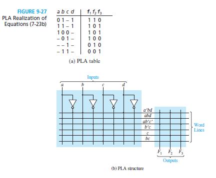
81 Fig 9-27 [RothKinney]
82 PAL Programmable Array Logic (PALs) are special cases of PLAs in which the AND array is programmable and the OR array is fixed. The PALs are less expensive than PLAs. Their functions are minimized independently of each other, since the AND terms cannot be shared between several OR gates. Fig 9-28 shows a PLA segment (a) unprogrammed and (b) programmed. The symbol from above represents an input buffer which is logically equivalent to:
83 Connections to the AND gate in a PAL are represented by X s, as shown [RothKinney]:
84 Fig 9-28 [RothKinney]: PAL segment.
85 Fig 9-29 [RothKinney]: Implementation of a full-adder using a PAL. Equations of the full adder are given on the right side:
86 Exclusive-or Gates The output of a exclusive- OR (XOR) gate is 1 only when only one of its inputs is 1, and 0 otherwise XNOR gate produces the negated function of an XOR gate XNOR function it is also called coincidence because it is 1 when the inputs are equal Truth table for XOR and XNOR functions [Wakerly]
87 Exclusive-OR gates Fig 6-69 [Wakerly]: Equivalent symbols for (a) XOR; (b) XNOR The most common are the leftmost symbols
88 Figure 6-68 [Wakerly]: Multigate designs for the 2-input XOR function: (a) AND-OR; (b) three-level NAND Exclusive-OR gates
89 Parity circuits XOR gates can be used in parity circuits, for determining the odd - parity of a number of bits: the output will be odd if the number of 1 bits is odd Fig 6-70 [Wakerly]: Cascanding XOR gates: (a) daisy-chainl (b) tree structure
90 Active levels Table 5-1 [Wakerly]: different naming conventions. We have used the convention from the last line of the table. At circuits, active low inputs and outputs are represented with an inverting bubble. Active levels are the level on which signals are doing their things [Wakerly].
In this lecture: Lecture 8: ROM & Programmable Logic Devices
 In this lecture: Lecture 8: ROM Programmable Logic Devices Dr Pete Sedcole Department of EE Engineering Imperial College London http://caseeicacuk/~nps/ (Floyd, 3 5, 3) (Tocci 2, 24, 25, 27, 28, 3 34)
CS302 Digital Logic Design Solved Objective Midterm Papers For Preparation of Midterm Exam
 CS302 Digital Logic Design Solved Objective Midterm Papers For Preparation of Midterm Exam MIDTERM EXAMINATION 2011 (October-November) Q-21 Draw function table of a half adder circuit? (2) Answer: - Page
Digital Electronics 8. Multiplexer & Demultiplexer
 1 Module -8 Multiplexers and Demultiplexers 1 Introduction 2 Principles of Multiplexing and Demultiplexing 3 Multiplexer 3.1 Types of multiplexer 3.2 A 2 to 1 multiplexer 3.3 A 4 to 1 multiplexer 3.4 Multiplex
COMBINATIONAL CIRCUIT
 Combinational circuit is a circuit in which we combine the different gates in the circuit, for example encoder, decoder, multiplexer and demultiplexer. Some of the characteristics of combinational circuits
Digital Applications (CETT 1415) Credit: 4 semester credit hours (3 hours lecture, 4 hours lab) Prerequisite: CETT 1403 & CETT 1405
 Credit: 4 semester credit hours (3 hours lecture, 4 hours lab) Prerequisite: CETT 1403 & CETT 1405") Digital Applications () Credit: 4 semester credit hours (3 hours lecture, 4 hours lab) Prerequisite: CETT 1403 & CETT 1405 Course Description This course covers digital techniques and numbering systems,
Digital Applications () Credit: 4 semester credit hours (3 hours lecture, 4 hours lab) Prerequisite: CETT 1403 & CETT 1405 Course Description This course covers digital techniques and numbering systems,
Unit 3. Logic Design
 EE 2: Digital Logic Circuit Design Dr Radwan E Abdel-Aal, COE Logic and Computer Design Fundamentals Unit 3 Chapter Combinational 3 Combinational Logic Logic Design - Introduction to Analysis & Design
Chapter 1: Digital logic
 Chapter 1: Digital logic I. Overview In PHYS 252, you learned the essentials of circuit analysis, including the concepts of impedance, amplification, feedback and frequency analysis. Most of the circuits
Module 4: Design and Analysis of Combinational Circuits 1. Module-4. Design and Analysis of Combinational Circuits
 1 Module-4 Design and Analysis of Combinational Circuits 4.1 Motivation: This topic develops the fundamental understanding and design of adder, substractor, code converter multiplexer, demultiplexer etc
Combinational Logic Design CH002
 Combinational Logic Design CH002 Figure 2.1 Circuit as a black box with inputs, outputs, and specifications Figure 2.2 Elements and nodes Figure 2.3 Combinational logic circuit Figure 2.4 Two OR implementations
CHW 261: Logic Design
 CHW 6: Logic Design Instructors: Prof. Hala Zayed Dr. Ahmed Shalaby http://www.bu.edu.eg/staff/halazayed4 http://bu.edu.eg/staff/ahmedshalaby4# Slide Copyright 6 by Pearson Education, Inc. Upper Saddle
UNIT-IV Combinational Logic
 UNIT-IV Combinational Logic Introduction: The signals are usually represented by discrete bands of analog levels in digital electronic circuits or digital electronics instead of continuous ranges represented
Digital Applications (CETT 1415) Credit: 4 semester credit hours (3 hours lecture, 4 hours lab) Prerequisite: CETT 1403 & CETT 1405
 Credit: 4 semester credit hours (3 hours lecture, 4 hours lab) Prerequisite: CETT 1403 & CETT 1405") Digital Applications (CETT 1415) Credit: 4 semester credit hours (3 hours lecture, 4 hours lab) Prerequisite: CETT 1403 & CETT 1405 Course Description This course covers digital techniques and numbering
Digital Applications (CETT 1415) Credit: 4 semester credit hours (3 hours lecture, 4 hours lab) Prerequisite: CETT 1403 & CETT 1405 Course Description This course covers digital techniques and numbering
Combinational logic. ! Regular logic: multiplexers, decoders, LUTs and FPGAs. ! Switches, basic logic and truth tables, logic functions
 Combinational logic! Switches, basic logic and truth tables, logic functions! Algebraic expressions to gates! Mapping to different gates! Discrete logic gate components (used in labs and 2)! Canonical
University of Technology
 University of Technology Lecturer: Dr. Sinan Majid Course Title: microprocessors 4 th year Lecture 7 & 8 NAND and XOR Implementations Combinational Design Procedure NAND-NAND & NOR-NOR Networks DeMorgan
Chapter 3 Combinational Logic Design
 Logic and Computer Design Fundamentals Chapter 3 Combinational Logic Design Part 2 Combinational Logic Overview Part -Implementation Technology and Logic Design Design Concepts Fundamental concepts of
Encoders. Lecture 23 5
 -A decoder with enable input can function as a demultiplexer a circuit that receives information from a single line and directs it to one of 2 n possible output lines. The selection of a specific output
Digital Electronics. Functions of Combinational Logic
 Digital Electronics Functions of Combinational Logic Half-dder Basic rules of binary addition are performed by a half adder, which has two binary inputs ( and B) and two binary outputs (Carry out and Sum).
Asst. Prof. Thavatchai Tayjasanant, PhD. Power System Research Lab 12 th Floor, Building 4 Tel: (02)
") 2145230 Aircraft Electricity and Electronics Asst. Prof. Thavatchai Tayjasanant, PhD Email: taytaycu@gmail.com aycu@g a co Power System Research Lab 12 th Floor, Building 4 Tel: (02) 218-6527 1 Chapter
2145230 Aircraft Electricity and Electronics Asst. Prof. Thavatchai Tayjasanant, PhD Email: taytaycu@gmail.com aycu@g a co Power System Research Lab 12 th Floor, Building 4 Tel: (02) 218-6527 1 Chapter
DO NOT COPY DO NOT COPY
 456 Chapter 5 Combinational Logic Design Practices The first PAL devices were invented at Monolithic Memories, Inc. (MMI) in 978 by John Birkner and H. T. Chua. The inventors earned U.S. patent number
Objective Questions. (a) Light (b) Temperature (c) Sound (d) all of these
 Light (b) Temperature (c) Sound (d) all of these") Objective Questions Module 1: Introduction 1. Which of the following is an analog quantity? (a) Light (b) Temperature (c) Sound (d) all of these 2. Which of the following is a digital quantity? (a) Electrical
Objective Questions Module 1: Introduction 1. Which of the following is an analog quantity? (a) Light (b) Temperature (c) Sound (d) all of these 2. Which of the following is a digital quantity? (a) Electrical
LOGIC GATES AND LOGIC CIRCUITS A logic gate is an elementary building block of a Digital Circuit. Most logic gates have two inputs and one output.
 LOGIC GATES AND LOGIC CIRCUITS A logic gate is an elementary building block of a Digital Circuit. Most logic gates have two inputs and one output. At any given moment, every terminal is in one of the two
EXPERIMENT NO 1 TRUTH TABLE (1)
") EPERIMENT NO AIM: To verify the Demorgan s theorems. APPARATUS REQUIRED: THEORY: Digital logic trainer and Patch cords. The digital signals are discrete in nature and can only assume one of the two values
EPERIMENT NO AIM: To verify the Demorgan s theorems. APPARATUS REQUIRED: THEORY: Digital logic trainer and Patch cords. The digital signals are discrete in nature and can only assume one of the two values
Odd-Prime Number Detector The table of minterms is represented. Table 13.1
 Odd-Prime Number Detector The table of minterms is represented. Table 13.1 Minterm A B C D E 1 0 0 0 0 1 3 0 0 0 1 1 5 0 0 1 0 1 7 0 0 1 1 1 11 0 1 0 1 1 13 0 1 1 0 1 17 1 0 0 0 1 19 1 0 0 1 1 23 1 0 1
Name: Class: Date: 1. As more electronic systems have been designed using digital technology, devices have become smaller and less powerful.
 Name: Class: Date: DE Midterm Review 2 True/False Indicate whether the statement is true or false. 1. As more electronic systems have been designed using digital technology, devices have become smaller
1. The decimal number 62 is represented in hexadecimal (base 16) and binary (base 2) respectively as
 and binary (base 2) respectively as") BioE 1310 - Review 5 - Digital 1/16/2017 Instructions: On the Answer Sheet, enter your 2-digit ID number (with a leading 0 if needed) in the boxes of the ID section. Fill in the corresponding numbered
BioE 1310 - Review 5 - Digital 1/16/2017 Instructions: On the Answer Sheet, enter your 2-digit ID number (with a leading 0 if needed) in the boxes of the ID section. Fill in the corresponding numbered
(CSC-3501) Lecture 6 (31 Jan 2008) Seung-Jong Park (Jay) CSC S.J. Park. Announcement
 Lecture 6 (31 Jan 2008) Seung-Jong Park (Jay) CSC S.J. Park. Announcement") Seung-Jong Park (Jay) http://www.csc.lsu.edu/~sjpark Computer Architecture (CSC-3501) Lecture 6 (31 Jan 2008) 1 Announcement 2 1 Reminder A logic circuit is composed of: Inputs Outputs Functional specification
Seung-Jong Park (Jay) http://www.csc.lsu.edu/~sjpark Computer Architecture (CSC-3501) Lecture 6 (31 Jan 2008) 1 Announcement 2 1 Reminder A logic circuit is composed of: Inputs Outputs Functional specification
UNIT III. Designing Combinatorial Circuits. Adders
 UNIT III Designing Combinatorial Circuits The design of a combinational circuit starts from the verbal outline of the problem and ends with a logic circuit diagram or a set of Boolean functions from which
EEE 301 Digital Electronics
 EEE 301 Digital Electronics Lecture 1 Course Contents Introduction to number systems and codes. Analysis and synthesis of digital logic circuits: Basic logic functions, Boolean algebra,combinational logic
Digital Electronic Concepts
 Western Technical College 10662137 Digital Electronic Concepts Course Outcome Summary Course Information Description Career Cluster Instructional Level Total Credits 4.00 Total Hours 108.00 This course
Number system: the system used to count discrete units is called number. Decimal system: the number system that contains 10 distinguished
 Number system: the system used to count discrete units is called number system Decimal system: the number system that contains 10 distinguished symbols that is 0-9 or digits is called decimal system. As
 Class Subject Code Subject Prepared By Lesson Plan for Time: Lesson. No 1.CONTENT LIST: Introduction to UnitII 2. SKILLS ADDRESSED: Learning I year, 02 sem CS6201 Digital Principles & System Design S.Seedhanadevi
EE19D Digital Electronics. Lecture 1: General Introduction
 EE19D Digital Electronics Lecture 1: General Introduction 1 What are we going to discuss? Some Definitions Digital and Analog Quantities Binary Digits, Logic Levels and Digital Waveforms Introduction to
Function Table of an Odd-Parity Generator Circuit
 Implementation of an Odd-Parity Generator Circuit The first step in implementing any circuit is to represent its operation in terms of a Truth or Function table. The function table for an 8-bit data as
CS302 - Digital Logic Design Glossary By
 CS302 - Digital Logic Design Glossary By ABEL : Advanced Boolean Expression Language; a software compiler language for SPLD programming; a type of hardware description language (HDL) Adder : A digital
Electronics. Digital Electronics
 Electronics Digital Electronics Introduction Unlike a linear, or analogue circuit which contains signals that are constantly changing from one value to another, such as amplitude or frequency, digital
Chapter 3 Digital Logic Structures
 Chapter 3 Digital Logic Structures Transistor: Building Block of Computers Microprocessors contain millions of transistors Intel Pentium 4 (2): 48 million IBM PowerPC 75FX (22): 38 million IBM/Apple PowerPC
Logic Design I (17.341) Fall Lecture Outline
 Fall Lecture Outline") Logic Design I (17.341) Fall 2011 Lecture Outline Class # 07 October 31, 2011 / November 07, 2011 Dohn Bowden 1 Today s Lecture Administrative Main Logic Topic Homework 2 Course Admin 3 Administrative
Logic Design I (17.341) Fall 2011 Lecture Outline Class # 07 October 31, 2011 / November 07, 2011 Dohn Bowden 1 Today s Lecture Administrative Main Logic Topic Homework 2 Course Admin 3 Administrative
Combinational Logic. Combinational Logic Design Process, Three State Buffers, Decoders, Multiplexers, Encoders, Demultiplexers, Other Considerations
 Combinational Logic Combinational Logic Design Process, Three State Buffers, Decoders, Multiplexers, Encoders, Demultiplexers, Other Considerations Copyright (c) 2012 Sean Key Combinational Logic Design
Chapter 4 Combinational Logic Circuits
 Chapter 4 Combinational Logic Circuits Chapter 4 Objectives Selected areas covered in this chapter: Converting logic expressions to sum-of-products expressions. Boolean algebra and the Karnaugh map as
COMPUTER ORGANIZATION & ARCHITECTURE DIGITAL LOGIC CSCD211- DEPARTMENT OF COMPUTER SCIENCE, UNIVERSITY OF GHANA
 COMPUTER ORGANIZATION & ARCHITECTURE DIGITAL LOGIC LOGIC Logic is a branch of math that tries to look at problems in terms of being either true or false. It will use a set of statements to derive new true
Fan in: The number of inputs of a logic gate can handle.
 Subject Code: 17333 Model Answer Page 1/ 29 Important Instructions to examiners: 1) The answers should be examined by key words and not as word-to-word as given in the model answer scheme. 2) The model
Gates and Circuits 1
 1 Gates and Circuits Chapter Goals Identify the basic gates and describe the behavior of each Describe how gates are implemented using transistors Combine basic gates into circuits Describe the behavior
Chapter 4 Combinational Logic Circuits
 Chapter 4 Combinational Logic Circuits Chapter 4 Objectives Selected areas covered in this chapter: Converting logic expressions to sum-of-products expressions. Boolean algebra and the Karnaugh map as
Chapter 3 Describing Logic Circuits Dr. Xu
 Chapter 3 Describing Logic Circuits Dr. Xu Chapter 3 Objectives Selected areas covered in this chapter: Operation of truth tables for AND, NAND, OR, and NOR gates, and the NOT (INVERTER) circuit. Boolean
2 Logic Gates THE INVERTER. A logic gate is an electronic circuit which makes logic decisions. It has one output and one or more inputs.
 2 Logic Gates A logic gate is an electronic circuit which makes logic decisions. It has one output and one or more inputs. THE INVERTER The inverter (NOT circuit) performs the operation called inversion
Combinational Logic Circuits. Combinational Logic
 Combinational Logic Circuits The outputs of Combinational Logic Circuits are only determined by the logical function of their current input state, logic 0 or logic 1, at any given instant in time. The
Logic Families. Describes Process used to implement devices Input and output structure of the device. Four general categories.
 Logic Families Characterizing Digital ICs Digital ICs characterized several ways Circuit Complexity Gives measure of number of transistors or gates Within single package Four general categories SSI - Small
Overview. This lab exercise requires. A windows computer running Xilinx WebPack A Digilent board. Contains material Digilent, Inc.
 Module 6: Combinational Circuit Blocks Revision: August 30, 2007 Overview This lab introduces several combinational circuits that are frequently used by digital designers, including a data selector (also
Laboratory Manual CS (P) Digital Systems Lab
 Digital Systems Lab") Laboratory Manual CS 09 408 (P) Digital Systems Lab INDEX CYCLE I A. Familiarization of digital ICs and digital IC trainer kit 1 Verification of truth tables B. Study of combinational circuits 2. Verification
Laboratory Manual CS 09 408 (P) Digital Systems Lab INDEX CYCLE I A. Familiarization of digital ICs and digital IC trainer kit 1 Verification of truth tables B. Study of combinational circuits 2. Verification
DIGITAL ELECTRONICS. Methods & diagrams : 1 Graph plotting : - Tables & analysis : - Questions & discussion : 6 Performance : 3
 DIGITAL ELECTRONICS Marking scheme : Methods & diagrams : 1 Graph plotting : - Tables & analysis : - Questions & discussion : 6 Performance : 3 Aim: This experiment will investigate the function of the
FPGA Based System Design
 FPGA Based System Design Reference Wayne Wolf, FPGA-Based System Design Pearson Education, 2004 Why VLSI? Integration improves the design: higher speed; lower power; physically smaller. Integration reduces
16 Multiplexers and De-multiplexers using gates and ICs. (74150, 74154)
") 16 Multiplexers and De-multiplexers using gates and ICs. (74150, 74154) Aim: To design multiplexers and De-multiplexers using gates and ICs. (74150, 74154) Components required: Digital IC Trainer kit,
16 Multiplexers and De-multiplexers using gates and ICs. (74150, 74154) Aim: To design multiplexers and De-multiplexers using gates and ICs. (74150, 74154) Components required: Digital IC Trainer kit,
PE713 FPGA Based System Design
 PE713 FPGA Based System Design Why VLSI? Dept. of EEE, Amrita School of Engineering Why ICs? Dept. of EEE, Amrita School of Engineering IC Classification ANALOG (OR LINEAR) ICs produce, amplify, or respond
2 Building Blocks. There is often the need to compare two binary values.
 2 Building Blocks 2.1 Comparators There is often the need to compare two binary values. This is done using a comparator. A comparator determines whether binary values A and B are: 1. A = B 2. A < B 3.
Topic Notes: Digital Logic
 Computer Science 220 Assembly Language & Comp. Architecture Siena College Fall 20 Topic Notes: Digital Logic Our goal for the next couple of weeks is to gain a reasonably complete understanding of how
Digital System Design
 UNIT III COMBINATIONAL LOGIC DESIGN Decoders: A decoder is a multiple-input, multiple-output logic circuit that converts coded inputs into coded outputs, where the input and output codes are different.
Computer Organization and Components
 Computer Organization and Components I5, fall 25 Lecture 7: Combinational Logic ssociate Professor, KTH Royal Institute of Technology ssistant Research ngineer, University of California, erkeley lides
Function Table of 74LS138, 3-to-8 Decoder +5V 6 G1 4 G2A 5 G2B. 4-to-16 Decoder using two 74LS139, 3-to-8 Decoder
 CS0 Digital Logic Design The XX8 -to-8 Decoder The -to-8, XX8 Decoder is also commonly used in logical circuits. Similar, to the -to- Decoder, the -to-8 Decoder has active-low outputs and three extra NOT
DIGITAL ELECTRONICS QUESTION BANK
 DIGITAL ELECTRONICS QUESTION BANK Section A: 1. Which of the following are analog quantities, and which are digital? (a) Number of atoms in a simple of material (b) Altitude of an aircraft (c) Pressure
Unit level 4 Credit value 15. Introduction. Learning Outcomes
 Unit 20: Unit code Digital Principles T/615/1494 Unit level 4 Credit value 15 Introduction While the broad field of electronics covers many aspects, it is digital electronics which now has the greatest
Gates and and Circuits
 Chapter 4 Gates and Circuits Chapter Goals Identify the basic gates and describe the behavior of each Describe how gates are implemented using transistors Combine basic gates into circuits Describe the
DELD UNIT 3. Question Option A Option B Option C Option D Correct Option A B C
 Class : S.E.Comp Matoshri College of Engineering and Research Center Nasik Department of Computer Engineering Digital Elecronics and Logic Design (DELD) UNIT - III Subject : DELD Sr. No. Question Option
UNIT-2: BOOLEAN EXPRESSIONS AND COMBINATIONAL LOGIC CIRCUITS
 UNIT-2: BOOLEAN EXPRESSIONS AND COMBINATIONAL LOGIC CIRCUITS STRUCTURE 2. Objectives 2. Introduction 2.2 Simplification of Boolean Expressions 2.2. Sum of Products 2.2.2 Product of Sums 2.2.3 Canonical
Introduction to CMOS VLSI Design (E158) Lecture 5: Logic
 Lecture 5: Logic") Harris Introduction to CMOS VLSI Design (E158) Lecture 5: Logic David Harris Harvey Mudd College David_Harris@hmc.edu Based on EE271 developed by Mark Horowitz, Stanford University MAH E158 Lecture 5 1
Harris Introduction to CMOS VLSI Design (E158) Lecture 5: Logic David Harris Harvey Mudd College David_Harris@hmc.edu Based on EE271 developed by Mark Horowitz, Stanford University MAH E158 Lecture 5 1
ECE 172 Digital Systems. Chapter 2 Digital Hardware. Herbert G. Mayer, PSU Status 6/30/2018
 ECE 172 Digital Systems Chapter 2 Digital Hardware Herbert G. Mayer, PSU Status 6/30/2018 1 Syllabus l Term Sharing l Standard Forms l Hazards l Decoders l PLA vs. PAL l PROM l Bibliography 2 Product Term
Reference. Wayne Wolf, FPGA-Based System Design Pearson Education, N Krishna Prakash,, Amrita School of Engineering
 FPGA Fabrics Reference Wayne Wolf, FPGA-Based System Design Pearson Education, 2004 CPLD / FPGA CPLD Interconnection of several PLD blocks with Programmable interconnect on a single chip Logic blocks executes
Subject: Analog and Digital Electronics Code:15CS32
 Subject: Analog and Digital Electronics Code:15CS32 Syllabus: The Basic Gates : Review of Basic Logic gates, Positive and Negative Logic, Introduction to HDL. Combinational Logic Circuits:Sum-of-Products
Logic diagram: a graphical representation of a circuit
 LOGIC AND GATES Introduction to Logic (1) Logic diagram: a graphical representation of a circuit Each type of gate is represented by a specific graphical symbol Truth table: defines the function of a gate
MAHARASHTRA STATE BOARD OF TECHNICAL EDUCATION (Autonomous) (ISO/IEC Certified) MODEL ANSWER
 (ISO/IEC Certified) MODEL ANSWER") Important Instructions to examiners: 1) The answers should be examined by key words and not as word-to-word as given in the model answer scheme. 2) The model answer and the answer written by candidate
Important Instructions to examiners: 1) The answers should be examined by key words and not as word-to-word as given in the model answer scheme. 2) The model answer and the answer written by candidate
Computer Hardware Engineering (IS1200) Computer Organization and Components (IS1500) Fall 2017 Lecture 7: Combinational Logic
 Computer Organization and Components (IS1500) Fall 2017 Lecture 7: Combinational Logic") Computer Hardware ngineering (I2) Computer Organization and Components (I5) Fall 27 Lecture 7: Combinational Logic Optional for I2, compulsory for I5 Fredrik Lundevall lides by David roman and Fredrik
Computer Hardware ngineering (I2) Computer Organization and Components (I5) Fall 27 Lecture 7: Combinational Logic Optional for I2, compulsory for I5 Fredrik Lundevall lides by David roman and Fredrik
LOGIC DIAGRAM: HALF ADDER TRUTH TABLE: A B CARRY SUM. 2012/ODD/III/ECE/DE/LM Page No. 1
 LOGIC DIAGRAM: HALF ADDER TRUTH TABLE: A B CARRY SUM K-Map for SUM: K-Map for CARRY: SUM = A B + AB CARRY = AB 22/ODD/III/ECE/DE/LM Page No. EXPT NO: DATE : DESIGN OF ADDER AND SUBTRACTOR AIM: To design
FUNCTION OF COMBINATIONAL LOGIC CIRCUIT
 HAPTER FUNTION OF OMBINATIONAL LOGI IRUIT OUTLINE HALF-ADDER ANF FULL ADDER IRUIT -BIT PARALLEL BINARY RIPPLE ARRY ADDER -BIT PARALLEL BINARY ARRY LOOK- AHEAD ADDER BD ADDER IRUIT DEODER ENODER MULTIPLEXER
Logic Symbols with Truth Tables INVERTER A B NAND A B C NOR C A B A B C XNOR A B C A B Digital Logic 1
 Slide Logic Symbols with Truth Tables UFFER INVERTER ND NND OR NOR XOR XNOR 6.7 Digital Logic Digital logic can be described in terms of standard logic symbols and their corresponding truth tables. The
Digital Logic Design ELCT 201
 Faculty of Information Engineering and Technology Dr. Haitham Omran and Dr. Wassim Alexan Digital Logic Design ELCT 201 Winter 2017 Midterm Exam Second Chance Please tick the box of your major: IET MET
Propagation Delay, Circuit Timing & Adder Design. ECE 152A Winter 2012
 Propagation Delay, Circuit Timing & Adder Design ECE 152A Winter 2012 Reading Assignment Brown and Vranesic 2 Introduction to Logic Circuits 2.9 Introduction to CAD Tools 2.9.1 Design Entry 2.9.2 Synthesis
Propagation Delay, Circuit Timing & Adder Design
 Propagation Delay, Circuit Timing & Adder Design ECE 152A Winter 2012 Reading Assignment Brown and Vranesic 2 Introduction to Logic Circuits 2.9 Introduction to CAD Tools 2.9.1 Design Entry 2.9.2 Synthesis
Digital Fundamentals. Introductory Digital Concepts
 Digital Fundamentals Introductory Digital Concepts Objectives Explain the basic differences between digital and analog quantities Show how voltage levels are used to represent digital quantities Describe
Lecture Topics ECE 341. Lecture # 4. Decoder. 2-to-4 Decoder Circuit
 ECE 34 Lecture # 4 Instructor: Zeshan Chishti zeshan@ece.pdx.edu October 8, 24 Portland State University Lecture Topics Decoders Multiplexers Programmable Logic Devices (PLDs) General Structure of PLDs
ECE/CoE 0132: FETs and Gates
 ECE/CoE 0132: FETs and Gates Kartik Mohanram September 6, 2017 1 Physical properties of gates Over the next 2 lectures, we will discuss some of the physical characteristics of integrated circuits. We will
Positive and Negative Logic
 Course: B.Sc. Applied Physical Science (Computer Science) Year & Sem.: IInd Year, Sem - IIIrd Subject: Computer Science Paper No.: IX Paper Title: Computer System Architecture Lecture No.: 4 Lecture Title:
Course Overview. Course Overview
 Course Overview Where does this course fit into the Electrical Engineering curriculum? Page 5 Course Overview Where does this course fit into the Computer Engineering curriculum? Page 6 3 Course Content
Digital Logic and Design (Course Code: EE222) Lecture 14: Combinational Contd.. Decoders/Encoders
 Lecture 14: Combinational Contd.. Decoders/Encoders") Indian Institute of Technology Jodhpur, Year 28 29 Digital Logic and Design (Course Code: EE222) Lecture 4: Combinational Contd.. Decoders/Encoders Course Instructor: Shree Prakash Tiwari Email: sptiwari@iitj.ac.in
Indian Institute of Technology Jodhpur, Year 28 29 Digital Logic and Design (Course Code: EE222) Lecture 4: Combinational Contd.. Decoders/Encoders Course Instructor: Shree Prakash Tiwari Email: sptiwari@iitj.ac.in
BEE 2233 Digital Electronics. Chapter 1: Introduction
 BEE 2233 Digital Electronics Chapter 1: Introduction Learning Outcomes Understand the basic concept of digital and analog quantities. Differentiate the digital and analog systems. Compare the advantages
Computer Architecture and Organization:
 Computer Architecture and Organization: L03: Register transfer and System Bus By: A. H. Abdul Hafez Abdul.hafez@hku.edu.tr, ah.abdulhafez@gmail.com 1 CAO, by Dr. A.H. Abdul Hafez, CE Dept. HKU Outlines
Multiple input gates. The AND gate
 Multiple input gates Inverters and buffers exhaust the possibilities for single-input gate circuits. What more can be done with a single logic signal but to buffer it or invert it? To explore more logic
TABLE 3-2 Truth Table for Code Converter Example
 997 by Prentice-Hall, Inc. Mano & Kime Upper Saddle River, New Jersey 7458 T-28 TABLE 3-2 Truth Table for Code Converter Example Decimal Digit Input BCD Output Excess-3 A B C D W Y Z 2 3 4 5 6 7 8 9 Truth
Winter 14 EXAMINATION Subject Code: Model Answer P a g e 1/28
 Subject Code: 17333 Model Answer P a g e 1/28 Important Instructions to examiners: 1) The answers should be examined by key words and not as word-to-word as given in the model answer scheme. 2) The model
SRV ENGINEERING COLLEGE SEMBODAI RUKMANI VARATHARAJAN ENGINEERING COLLEGE SEMBODAI
 SEMBODAI RUKMANI VARATHARAJAN ENGINEERING COLLEGE SEMBODAI 6489 (Approved By AICTE,Newdelhi Affiliated To ANNA UNIVERSITY::Chennai) CS 62 DIGITAL ELECTRONICS LAB (REGULATION-23) LAB MANUAL DEPARTMENT OF
1.) If a 3 input NOR gate has eight input possibilities, how many of those possibilities result in a HIGH output? (a.) 1 (b.) 2 (c.) 3 (d.) 7 (e.
 If a 3 input NOR gate has eight input possibilities, how many of those possibilities result in a HIGH output? (a.) 1 (b.) 2 (c.) 3 (d.) 7 (e.") Name: Multiple Choice 1.) If a 3 input NOR gate has eight input possibilities, how many of those possibilities result in a HIGH output? (a.) 1 (b.) 2 (c.) 3 (d.) 7 (e.) 8 2.) The output of an OR gate with
Name: Multiple Choice 1.) If a 3 input NOR gate has eight input possibilities, how many of those possibilities result in a HIGH output? (a.) 1 (b.) 2 (c.) 3 (d.) 7 (e.) 8 2.) The output of an OR gate with
LIST OF EXPERIMENTS. KCTCET/ /Odd/3rd/ETE/CSE/LM
 LIST OF EXPERIMENTS. Study of logic gates. 2. Design and implementation of adders and subtractors using logic gates. 3. Design and implementation of code converters using logic gates. 4. Design and implementation
EE40 Lecture 35. Prof. Chang-Hasnain. 12/5/07 Reading: Ch 7, Supplementary Reader
 EE4 Lecture 35 2/5/7 Reading: Ch 7, Supplementary Reader EE4 all 26 Slide Week 5 OUTLINE Need for Input Controlled Pull-Up CMOS Inverter nalysis CMOS Voltage Transfer Characteristic Combinatorial logic
Digital Logic ircuits Circuits Fundamentals I Fundamentals I
 Digital Logic Circuits Fundamentals I Fundamentals I 1 Digital and Analog Quantities Electronic circuits can be divided into two categories. Digital Electronics : deals with discrete values (= sampled
Data output signals May or may not be same a input signals
 Combinational Logic Part 2 We ve been looking at simple combinational logic elements Gates, buffers, and drivers Now ready to go on to larger blocks MSI - Medium Scale Integration or Integrate Circuits
IES Digital Mock Test
 . The circuit given below work as IES Digital Mock Test - 4 Logic A B C x y z (a) Binary to Gray code converter (c) Binary to ECESS- converter (b) Gray code to Binary converter (d) ECESS- To Gray code
Programmable Logic Arrays (PLAs)
") Programmable Logic Regular logic Programmable Logic rrays Multiplexers/ecoders ROMs Field Programmable Gate rrays Xilinx Vertex Random Logic Full ustom esign S 5 - Fall 25 Lec. #3: Programmable Logic -
Programmable Logic Regular logic Programmable Logic rrays Multiplexers/ecoders ROMs Field Programmable Gate rrays Xilinx Vertex Random Logic Full ustom esign S 5 - Fall 25 Lec. #3: Programmable Logic -
COMBINATIONAL and SEQUENTIAL LOGIC CIRCUITS Hardware implementation and software design
 PH-315 COMINATIONAL and SEUENTIAL LOGIC CIRCUITS Hardware implementation and software design A La Rosa I PURPOSE: To familiarize with combinational and sequential logic circuits Combinational circuits
Lecture 02: Digital Logic Review
 CENG 3420 Lecture 02: Digital Logic Review Bei Yu byu@cse.cuhk.edu.hk CENG3420 L02 Digital Logic. 1 Spring 2017 Review: Major Components of a Computer CENG3420 L02 Digital Logic. 2 Spring 2017 Review:
JEFFERSON COLLEGE COURSE SYLLABUS ETC255 INTRODUCTION TO DIGITAL CIRCUITS. 6 Credit Hours. Prepared by: Dennis Eimer
 JEFFERSON COLLEGE COURSE SYLLABUS ETC255 INTRODUCTION TO DIGITAL CIRCUITS 6 Credit Hours Prepared by: Dennis Eimer Revised Date: August, 2007 By Dennis Eimer Division of Technology Dr. John Keck, Dean
Chapter 3. H/w s/w interface. hardware software Vijaykumar ECE495K Lecture Notes: Chapter 3 1
 Chapter 3 hardware software H/w s/w interface Problems Algorithms Prog. Lang & Interfaces Instruction Set Architecture Microarchitecture (Organization) Circuits Devices (Transistors) Bits 29 Vijaykumar
Approximate Hybrid Equivalent Circuits. Again, the impedance looking into the output terminals is infinite so that. conductance is zero.
 Again, the impedance looking into the output terminals is infinite so that conductance is zero. Hence, the four h-parameters of an ideal transistor connected in CE transistor are The hybrid equivalent