EXPERIMENT NO 1 TRUTH TABLE (1)
|
|
|
- Isaac Morris
- 5 years ago
- Views:
Transcription
1 EPERIMENT NO AIM: To verify the Demorgan s theorems. APPARATUS REQUIRED: THEORY: Digital logic trainer and Patch cords. The digital signals are discrete in nature and can only assume one of the two values O and.a number system based on these two digit is known as binary number system. This is basic of all digital systems like computers, calculators etc. Binary Variables can be represented by letter symbol such A,B,,Y. The variable can have only one of the two variable possible values at anytime i.e. or Demerger s Theorems can be proved by fist considering the two variable case and then extending this result. DEMORGAN S THEOREM S: PROCEDURE: DEMORGAN S THE -. Make the circuit dia. As in fig and connect the inputs of the gate to the input state sockets A,B and C and output to the output indicators. 2. Set the input combinations one by one by putting input state switches A,B and C either in or state. 3. Now verify the output with the help of Truth Table () TRUTH TABLE () A B C A B C A.B.C A.B.C A+B+C DEMORGAN S THEOREM-2: Make the circuit dia. As shown in fig and connect the inputs o the gate to the input state sockets A,B and C and output to the output indicators.
2 . Set the input combinations one by the putting input state switches A,B and C either or state. 2. Now verify the output with the help of Truth Table (2). TRUTH TABLE (2) A B C A B C A.B.C A+B+C A+B+C RESULT:
3 Experiment No.2 Aim: To study and verify the Truth Tables of AND, OR, NOT, NAND, NOR EOR logic gates for positive logic. Apparatus Required: Theory: Digital logic trainer and Patch cords AND Gate: A multi-input circuit in which the output is only if all inputs are.the symbolic representation of the AND gate is: The AND gate is an electronic circuit that gives a high output () only if all its inputs are high. A dot (.) is used to show the AND operation i.e. A.B. OR gate : A multi-input circuit in which the output is when any input is. The symbolic representation of the OR gate is shown: The OR gate is an electronic circuit that gives a high output () if one or more of its inputs are high. A plus (+) is used to show the OR operation. NOT gate: The output is when the input is, and the output is when the input is. The symbolic representation of an inverter is : The NOT gate is an electronic circuit that produces an inverted version of the input at its output. It is also known as an inverter. If the input variable is A, the inverted output is known as NOT A. This is also shown as A', or A with a bar over the top, as shown at the outputs. NAND gate: AND followed by INVERT. It is also known as universal gate.the symbolic representation of the NAND gate is:
4 This is a NOT-AND gate which is equal to an AND gate followed by a NOT gate. The outputs of all NAND gates are high if any of the inputs are low. The symbol is an AND gate with a small circle on the output. The small circle represents inversion. NOR gate: OR followed by inverter. It is also known as universal gate.the symbolic representation is: This is a NOT-OR gate which is equal to an OR gate followed by a NOT gate. The outputs of all NOR gates are low if any of the inputs are high. The symbol is an OR gate with a small circle on the output. The small circle represents inversion. EOR gate: The output of the Exclusive OR gate, is when it s two inputs are the same and it s output is when its two inputs are different.it is also known as Anti-coincidence gate. The 'Exclusive-OR' gate is a circuit which will give a high output if either, but not both, of its two inputs are high. An encircled plus sign ( ) is used to show the EOR operation. Observation Table: LED ON(RED light): Logic LED OFF(Green Light): Logic Input variables: A,B Output variable: Y S.No Input(A) LED Calculation: Input(B) LED Output (OR) Y = A Output (AND) Y=AB Output (OR) Y=A+B Output (NAND) Y = AB Output (NOR) Y= A+B Output (OR) Y=A B Results and Analysis:
5 NOT Gate: When logic is applied to one of NOT gate of 744 IC, then output becomes zero. When input LED is ON (RED), the output LED become OFF (Green) vice versa. OR Gate: The output of an OR gate is a if one or the other or both of the inputs are, but a if both inputs are. When One or the other or Both of the input LEDS are ON (RED Light), then output LED is ON(RED) otherwise Output LED is OFF(Green Light) AND Gate: The output of an AND gate is only if both its inputs are. For all other possible inputs the output is.when both the LEDS are On, then output LED is ON (RED Light) otherwise Output LED is OFF. NOR Gate: The output of the NOR gate is a if both inputs are but a if one or the other or both the inputs are. NAND Gate: The output of the NAND gate is a if both inputs are but a if one or the other or both the inputs are. EOR gate: The output of the OR gate is a if either but not both inputs are and a if the inputs are both or both. RESULT:
6 EPERIMENT NO 3 AIM: - To verify the Half Adder & Full Adder APPARATUS REQUIRED: Digital logic trainer and Patch cords. THEORY: Half Adder With the help of half adder, we can design circuits that are capable of performing simple addition with the help of logic gates. Let us first take a look at the addition of single bits. + = + = + = + = These are the least possible single-bit combinations. But the result for + is. Though this problem can be solved with the help of an EOR Gate, if you do care about the output, the sum result must be rewritten as a 2-bit output. Thus the above equations can be written as + = + = + = + = Here the output of becomes the carry-out. The result is shown in a truth-table below. SUM is the normal output and CARRY is the carry-out. INPUTS OUTPUTS A B SUM CARRY From the equation it is clear that this -bit adder can be easily implemented with the help of EOR Gate for the output SUM and an AND Gate for the carry. Take a look at the implementation below.

7 For complex addition, there may be cases when you have to add two 8-bit bytes together. This can be done only with the help of full-adder logic. Full Adder This type of adder is a little more difficult to implement than a half-adder. The main difference between a half-adder and a full-adder is that the full-adder has three inputs and two outputs. The first two inputs are A and B and the third input is an input carry designated as CIN. When a full adder logic is designed we will be able to string eight of them together to create a byte-wide adder and cascade the carry bit from one adder to the next. The output carry is designated as COUT and the normal output is designated as S. Take a look at the truth-table. INPUTS OUTPUTS A B CIN COUT S From the above truth-table, the full adder logic can be implemented. We can see that the output S is an EOR between the input A and the half-adder SUM output with B and CIN inputs. We must also note that the COUT will only be true if any of the two inputs out of the three are HIGH. Thus, we can implement a full adder circuit with the help of two half adder circuits. The first will half adder will be used to add A and B to produce a partial Sum. The second half adder logic can be used to


8 add CIN to the Sum produced by the first half adder to get the final S output. If any of the half adder logic produces a carry, there will be an output carry. Thus, COUT will be an OR function of the half-adder Carry outputs.. Single Bit full Adder With this type of symbol, we can add two bits together taking a carry from the next lower order of magnitude, and sending a carry to the next higher order of magnitude. In a computer, for a multi-bit operation, each bit must be represented by a full adder and must be added simultaneously. Thus, to add two 8-bit numbers, you will need 8 full adders which can be formed by cascading two of the 4-bit blocks. The addition of two 4-bit numbers is shown below. RESULT:
9 EPERIMENT NO 4 AIM: To verify the Hlf Substactor & Full Substractor APPARATUS REQUIRED: Digital logic trainer and Patch cords. THEORY The arithmetic operation, subtraction of two binary digits has four possible elementary operations, namely, - = - = - = - = with borrow In all operations, each subtrahend bit is subtracted from the minuend bit. In case of the second operation the minuend bit is smaller than the subtrahend bit, hence is borrowed. HALF SUBTRACTOR: A combinational circuit which performs the subtraction of two bits is called half subtractor. The input variables designate the minuend and the subtrahend bit, whereas the output variables produce the difference and borrow bits. Half subtractor The half-subtractor is a combinational circuit which is used to perform subtraction of two bits. It has two inputs, (minuend) and Y (subtrahend) and two outputs D (difference) and B (borrow). INPUTS OUTPUTS A B Diff Borrow

 and so allows cascading which results in the possibility of multi-bit subtraction.")
10 Full subtractor A combinational circuit which performs the subtraction of three input bits is called full subtractor. The three input bits include two significant bits and a previous borrow bit. A full subtractor circuit can be implemented with two half subtractors and one OR gate. As in the case of the addition using logic gates, a full subtractor is made by combining two half-subtractors and an additional OR-gate. A full subtractor has the borrow in capability (denoted as BOR IN in the diagram below) and so allows cascading which results in the possibility of multi-bit subtraction. The circuit diagram for a full subtractor is given below. INPUTS OUTPUTS A B CIN Diff Borrow RESULT:
11 EPERIMENT NO 5 AIM: -To verify the characteristic table of RS, D, JK, and T Flip flops. APPARATUS REQUIRED: S.No Name of the Apparatus Range Quantity. Digital IC trainer kit 2. NOR gate IC NOT gate IC AND gate ( three input ) IC NAND gate IC Connecting wires As required THEORY: A Flip Flop is a sequential device that samples its input signals and changes its output states only at times determined by clocking signal. Flip Flops may vary in the number of inputs they possess and the manner in which the inputs affect the binary states. RS FLIP FLOP: The clocked RS flip flop consists of NAND gates and the output changes its state with respect to the input on application of clock pulse. When the clock pulse is high the S and R inputs reach the second level NAND gates in their complementary form. The Flip Flop is reset when the R input high and S input is low. The Flip Flop is set when the S input is high and R input is low. When both the inputs are high the output is in an indeterminate state. D FLIP FLOP: To eliminate the undesirable condition of indeterminate state in the SR Flip Flop when both inputs are high at the same time, in the D Flip Flop the inputs are never made equal at the same time. This is obtained by making the two inputs complement of each other. JK FLIP FLOP:
12 The indeterminate state in the SR Flip-Flop is defined in the JK Flip Flop. JK inputs behave like S and R inputs to set and reset the Flip Flop. The output Q is ANDed with K input and the clock pulse, similarly the output Q is ANDed with J input and the Clock pulse. When the clock pulse is zero both the AND gates are disabled and the Q and Q output retain their previous values. When the clock pulse is high, the J and K inputs reach the NOR gates. When both the inputs are high the output toggles continuously. This is called Race around condition and this must be avoided. T FLIP FLOP: This is a modification of JK Flip Flop, obtained by connecting both inputs J and K inputs together. T Flip Flop is also called Toggle Flip Flop. RS FLIP FLOP LOGIC SYMBOL: CIRCUIT DIAGRAM:
13 CHARACTERISTIC TABLE: COLLEGE NAME, CITY CLOCK INPUT PRESENT NET PULSE S R STATE (Q) STATE(Q+) STATUS D FLIP FLOP LOGIC SYMBOL: CHARACTERISTIC TABLE: CLOCK PULSE INPUT D PRESENT STATE (Q) NET STATE(Q+) STATUS
14 JK FLIP FLOP LOGIC SYMBOL: CIRCUIT DIAGRAM: CHARACTERISTIC TABLE: CLOCK INPUT PRESENT NET PULSE J K STATE (Q) STATE(Q+) STATUS
15 LOGIC SYMBOL: T FLIP FLOP CIRCUIT DIAGRAM: CHARACTERISTIC TABLE: CLOCK PULSE INPUT T PRESENT STATE (Q) NET STATE(Q+) STATUS PROCEDURE:. Connections are given as per the circuit diagrams. 2. For all the ICs 7 th pin is grounded and 4 th pin is given +5 V supply. 3. Apply the inputs and observe the status of all the flip flops. RESULT:

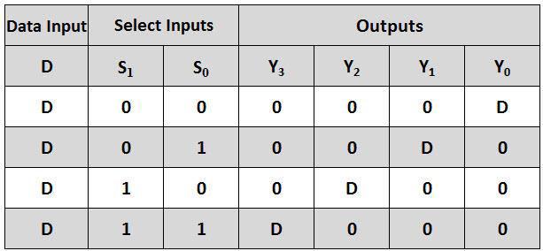
16 Experiment No. 6 AIM: The main objective of this experiment is to study the working principle of 4: multiplexer. APPARATUS REQUIRESD: THEORY: Trainer Kit, 23V power supply. S multiplexers are circuits that can select one of many inputs. 4: is the most popular multiplexer and as the name indicates it has 4 inputs with only output. It has 2 data selector inputs namely S,S, at which the control bits are applied. S,S,4 are the point at which the controls are applied.d,d, represent the inputs bits. Only one of these will be transmitted to the output. But which one of the inputs will be transmitted will depend on the values of the controls. If for instance S S=, then the first AND gate is enabled and all others are disabled. Hence D is transmitted. Again if S2 S=, then the second AND enable and D will be transmitted. It is the control nibble that decide which inputs will be transmitted. Therefore, an input Dn is selected corresponding to the decimal number n representing S S. PROCEDURE:. Connect 2 pin power cord of the trainer to the 23V supply. 2. Make strobe switch at low position. 3. Set the data inputs (D-D5) to either or. 4. To verify the multiplexer action set the address line as shown in the truth table & observe the output condition. 5. Observe the effect of strobe input on the output. TRUTH TABLE RESULT: The truth table of the mux is verified from the theoretical truth table.
17 EPERIMENT No:7 AIM: Study of working principle of :4 demultiplexer using IC-4445 APPARATUS REQUIRED: THEORY: Trainer kit, power supply. Demultiplexer as t he name indicates, it has only data input D with 4 outputs namely Y,YY2 Y3 It has two data selector inputs namely S,S, at which control bits are applied. The data bit is transmitted to the data bit Y,YY2 Y3 of the output lines. Which particular output line will be chosen will depend on the value of S3,S2,S,S the control input. Consider the case when S S= now the upper AND gate is enable while all other AND gate are disabled. Hence it is not possible to activate any output other than Y. Thus Y=D, if D is low Y will be low and if D is high, Y will be high. Considering another case,s,s=. We find that Y is activated because second AND gate is enable. Similarly if S S=. The sixteenth AND gate will be enabled and Y5 Will be activated. Thus if D is high then all values other then the correct value of activated Y output, will be low. PROCEDURE:. Connect 2 pin power cord of trainer to 23V supply. 2. Make strobe switch at low position. 3. Set the data input (D-D5) to either or 4. To verify the Demultiplexer action, set the address line as shown n in truth table and observe the output condition. 5. Observe the effect of strobe input on the output. RESULT: The truth Table for :4 Demultiplexer is verified.
18
19 EPERIMENT NO 8 AIM: To study the Encoder and Decoder Circuits. APPARATUS REQUIRED: Encoder and Decoder kit, patch cords etc. THEORY: Combinational logic circuit are digital circuits made up to gates and inverters. An example of this type is the Exclusive OR circuit. The most common type are Decoders, Multiplexers, Comparators and Convertors. A widely used type of decoder is the BCD To decimal Decoder, the input to the decoder is a parallel 4-Bit Binary number from through and the circuit provides ten discrete outputs representing decimal numbers through 9. The output of such a decoder is generally used to operate a lighted number display. Some codes are binary code (Natural BCD), Excess-3 code and gray code. 4 bits are required to represent the decimal digits in these codes. An Encoder is a combinational logic circuit that essentially performs a reverse decoder function. An encoder accepts and active one of its inputs representing a digit, such as a decimal digit or octal digit and converts it to a coded output, such as a binary or BCD. Encoders can also be devised to encode various symbols and alphabetic characters. This process of converting from familiar symbols or numbers to a coded format is called Encoding. PROCEDURE: A. Decimal to BCD Encoder:. Connect nine logic inputs of IC 7447 to logic inputs & through patch cords. 2. Connect four logic outputs to outputs indicators through patch cords. 3. Switch ON the instrument using ON/OFF toggle switch provided on the front panel 4. Verify the observation Table no (). means either or.
20 OBSERVATION T ABLE () Decimal Inputs BCD Outputs Q D Q C Q B Q A 9 B. Binary to Gray Code Convertor:. Connect four logic inputs (A,B,C,D) OF Binary to gray code convertor to logic inputs & through path cords. 2. Connect four logic outputs (Q A,Q B,Q C& Q D ) of the convertor to four logic output indicators through patch cords. 3. Switch ON the instrument using ON/OFF toggle switch provided on front panel. 4. Verify the observation table (2) D C B A Q D Q C Q B Q A C. BCD to Decimal Decoder:. Connect four logic inputs (A,B,C,D) of BCD to Decimal code convertor to logic inputs & through patch cords. 2. Connect ten logic outputs of the convertor to ten logic output indicators through patch cords. 3. Switch ON the instrument using ON/OFF toggle switch provided front panel. 4. Verify the observation table (3).
21 OBSERVATION TABLE (3) BCD Inputs Decimal Outputs D C B A D. BCD to 7- segment Decoder:. Connect four logic inputs (A,B,C,D) OF BCD to 7- Segment Decoder to logic inputs & through patch cords. 2. Connect seven logic outputs (Q,Q2,Q3,Q4,Q5,Q6,Q7) of the convertor to inputs of 7- segment display through patch cords i.e. connect Q output to resistance R,Q2 to R2,Q3 to R3,Q4, to R4 and so on.. 3. Switch ON the instrument using ON/OFF toggle switch provided on front panel. 4. Verify the observation table (4). OBSERVATION TABLE (4) BCD Inputs 7-Segment D C B A Outputs RESULT:
22 EPERIMENT No:9 AIM: -To design and verify the truth table of a 4 Multiplexer & 4 Demultiplexer. APPARATUS REQUIRED: S.No Name of the Apparatus Range Quantity. Digital IC trainer kit 2. OR gate IC NOT gate IC AND gate ( three input ) IC Connecting wires As required THEORY: Multiplexer is a digital switch which allows digital information from several sources to be routed onto a single output line. The basic multiplexer has several data input lines and a single output line. The selection of a particular input line is controlled by a set of selection lines. Normally, there are 2 n input lines and n selector lines whose bit combinations determine which input is selected. Therefore, multiplexer is many into one and it provides the digital equivalent of an analog selector switch. A Demultiplexer is a circuit that receives information on a single line and transmits this information on one of 2 n possible output lines. The selection of specific output line is controlled by the values of n selection lines. DESIGN: 4 MULTIPLEER LOGIC SYMBOL:
23 TRUTH TABLE: S.No SELECTION INPUT OUTPUT S S2 Y. I 2. I 3. I 2 4. I 3 CIRCUIT DIAGRAM:
24 4 DEMULTIPLEER LOGIC SYMBOL: TRUTH TABLE: S.No INPUT OUTPUT S S2 Din Y Y Y2 Y
25 CIRCUIT DIAGRAM: COLLEGE NAME, CITY PROCEDURE:. Connections are given as per the circuit diagrams. 2. For all the ICs 7 th pin is grounded and 4 th pin is given +5 V supply. 3. Apply the inputs and verify the truth table for the multiplexer & demultiplexer. RESULT:
Department of Electronics and Communication Engineering
 Department of Electronics and Communication Engineering Sub Code/Name: BEC3L2- DIGITAL ELECTRONICS LAB Name Reg No Branch Year & Semester : : : : LIST OF EXPERIMENTS Sl No Experiments Page No Study of
COMBINATIONAL CIRCUIT
 Combinational circuit is a circuit in which we combine the different gates in the circuit, for example encoder, decoder, multiplexer and demultiplexer. Some of the characteristics of combinational circuits
LOGIC DIAGRAM: HALF ADDER TRUTH TABLE: A B CARRY SUM. 2012/ODD/III/ECE/DE/LM Page No. 1
 LOGIC DIAGRAM: HALF ADDER TRUTH TABLE: A B CARRY SUM K-Map for SUM: K-Map for CARRY: SUM = A B + AB CARRY = AB 22/ODD/III/ECE/DE/LM Page No. EXPT NO: DATE : DESIGN OF ADDER AND SUBTRACTOR AIM: To design
LIST OF EXPERIMENTS. KCTCET/ /Odd/3rd/ETE/CSE/LM
 LIST OF EXPERIMENTS. Study of logic gates. 2. Design and implementation of adders and subtractors using logic gates. 3. Design and implementation of code converters using logic gates. 4. Design and implementation
SRV ENGINEERING COLLEGE SEMBODAI RUKMANI VARATHARAJAN ENGINEERING COLLEGE SEMBODAI
 SEMBODAI RUKMANI VARATHARAJAN ENGINEERING COLLEGE SEMBODAI 6489 (Approved By AICTE,Newdelhi Affiliated To ANNA UNIVERSITY::Chennai) CS 62 DIGITAL ELECTRONICS LAB (REGULATION-23) LAB MANUAL DEPARTMENT OF
UNIT-IV Combinational Logic
 UNIT-IV Combinational Logic Introduction: The signals are usually represented by discrete bands of analog levels in digital electronic circuits or digital electronics instead of continuous ranges represented
Laboratory Manual CS (P) Digital Systems Lab
 Digital Systems Lab") Laboratory Manual CS 09 408 (P) Digital Systems Lab INDEX CYCLE I A. Familiarization of digital ICs and digital IC trainer kit 1 Verification of truth tables B. Study of combinational circuits 2. Verification
Laboratory Manual CS 09 408 (P) Digital Systems Lab INDEX CYCLE I A. Familiarization of digital ICs and digital IC trainer kit 1 Verification of truth tables B. Study of combinational circuits 2. Verification
Module 4: Design and Analysis of Combinational Circuits 1. Module-4. Design and Analysis of Combinational Circuits
 1 Module-4 Design and Analysis of Combinational Circuits 4.1 Motivation: This topic develops the fundamental understanding and design of adder, substractor, code converter multiplexer, demultiplexer etc
DEPARTMENT OF ELECTRICAL & ELECTRONICS ENGINEERING
 DEPARTMENT OF ELECTRICAL & ELECTRONICS ENGINEERING (Regulation 2013) EE 6311 LINEAR AND DIGITAL INTEGRATED CIRCUITS LAB MANUAL 1 SYLLABUS OBJECTIVES: Working Practice in simulators / CAD Tools / Experiment
2 Building Blocks. There is often the need to compare two binary values.
 2 Building Blocks 2.1 Comparators There is often the need to compare two binary values. This is done using a comparator. A comparator determines whether binary values A and B are: 1. A = B 2. A < B 3.
LOGIC GATES AND LOGIC CIRCUITS A logic gate is an elementary building block of a Digital Circuit. Most logic gates have two inputs and one output.
 LOGIC GATES AND LOGIC CIRCUITS A logic gate is an elementary building block of a Digital Circuit. Most logic gates have two inputs and one output. At any given moment, every terminal is in one of the two
Digital Electronics 8. Multiplexer & Demultiplexer
 1 Module -8 Multiplexers and Demultiplexers 1 Introduction 2 Principles of Multiplexing and Demultiplexing 3 Multiplexer 3.1 Types of multiplexer 3.2 A 2 to 1 multiplexer 3.3 A 4 to 1 multiplexer 3.4 Multiplex
Dhanalakshmi College of Engineering
 Dhanalakshmi College of Engineering Manimangalam, Tambaram, Chennai 601 301 DEPARTMENT OF ELECTRICAL AND ELECTRONICS ENGINEERING EE6311 LINEAR AND DIGITAL INTEGRATED CIRCUITS LABORATORY III SEMESTER -
COMBINATIONAL LOGIC CIRCUIT First Class. Dr. AMMAR ABDUL-HAMED KHADER
 COMBINATIONAL LOGIC CIRCUIT First Class 1 BASIC ADDER Adders are important in computers and also in other types of digital system in which numerical data are processed. An understanding of the basic operation
Digital Applications (CETT 1415) Credit: 4 semester credit hours (3 hours lecture, 4 hours lab) Prerequisite: CETT 1403 & CETT 1405
 Credit: 4 semester credit hours (3 hours lecture, 4 hours lab) Prerequisite: CETT 1403 & CETT 1405") Digital Applications () Credit: 4 semester credit hours (3 hours lecture, 4 hours lab) Prerequisite: CETT 1403 & CETT 1405 Course Description This course covers digital techniques and numbering systems,
Digital Applications () Credit: 4 semester credit hours (3 hours lecture, 4 hours lab) Prerequisite: CETT 1403 & CETT 1405 Course Description This course covers digital techniques and numbering systems,
COLLEGE OF ENGINEERING, NASIK
 Pune Vidyarthi Griha s COLLEGE OF ENGINEERING, NASIK LAB MANUAL DIGITAL ELECTRONICS LABORATORY Subject Code: 2246 27-8 PUNE VIDYARTHI GRIHA S COLLEGE OF ENGINEERING,NASHIK. INDEX Batch : - Sr.No Title
Winter 14 EXAMINATION Subject Code: Model Answer P a g e 1/28
 Subject Code: 17333 Model Answer P a g e 1/28 Important Instructions to examiners: 1) The answers should be examined by key words and not as word-to-word as given in the model answer scheme. 2) The model
UNIT III. Designing Combinatorial Circuits. Adders
 UNIT III Designing Combinatorial Circuits The design of a combinational circuit starts from the verbal outline of the problem and ends with a logic circuit diagram or a set of Boolean functions from which
Experiment # 3 Combinational Circuits (I) Binary Addition and Subtraction
 Binary Addition and Subtraction") Experiment # 3 Combinational Circuits (I) Binary Addition and Subtraction Objectives: 1. To study adder and subtractor circuits using logic gates. 2. To construct and test various adders and subtractor
Experiment # 3 Combinational Circuits (I) Binary Addition and Subtraction Objectives: 1. To study adder and subtractor circuits using logic gates. 2. To construct and test various adders and subtractor
DIGITAL CIRCUITS AND SYSTEMS ASSIGNMENTS 1 SOLUTIONS
 DIGITAL CIRCUITS AND SYSTEMS ASSIGNMENTS 1 SOLUTIONS 1. Analog signal varies continuously between two amplitudes over the given interval of time. Between these limits of amplitude and time, the signal
Asst. Prof. Thavatchai Tayjasanant, PhD. Power System Research Lab 12 th Floor, Building 4 Tel: (02)
") 2145230 Aircraft Electricity and Electronics Asst. Prof. Thavatchai Tayjasanant, PhD Email: taytaycu@gmail.com aycu@g a co Power System Research Lab 12 th Floor, Building 4 Tel: (02) 218-6527 1 Chapter
2145230 Aircraft Electricity and Electronics Asst. Prof. Thavatchai Tayjasanant, PhD Email: taytaycu@gmail.com aycu@g a co Power System Research Lab 12 th Floor, Building 4 Tel: (02) 218-6527 1 Chapter
Fan in: The number of inputs of a logic gate can handle.
 Subject Code: 17333 Model Answer Page 1/ 29 Important Instructions to examiners: 1) The answers should be examined by key words and not as word-to-word as given in the model answer scheme. 2) The model
 DHANALAKSHMI COLLEGE OF ENGINEERING MANIMANGALAM. TAMBARAM, CHENNAI B.E. ELECTRICAL AND ELECTRONICS ENGINEERING III SEMESTER EE6311 Linear and Digital Integrated Circuits Laboratory LABORATORY MANUAL CLASS:
Experiment # 4. Binary Addition & Subtraction. Eng. Waleed Y. Mousa
 Experiment # 4 Binary Addition & Subtraction Eng. Waleed Y. Mousa 1. Objectives: 1. To study adder and subtractor circuits using logic gates. 2. To construct and test various adders and subtractor circuits.
UNIT-2: BOOLEAN EXPRESSIONS AND COMBINATIONAL LOGIC CIRCUITS
 UNIT-2: BOOLEAN EXPRESSIONS AND COMBINATIONAL LOGIC CIRCUITS STRUCTURE 2. Objectives 2. Introduction 2.2 Simplification of Boolean Expressions 2.2. Sum of Products 2.2.2 Product of Sums 2.2.3 Canonical
Sr. No. Instrument Specifications. TTL (Transistor-Transistor Logic) based on bipolar junction transistors
 based on bipolar junction transistors") MIT College of Engineering, Pune. Department of Electronics & Telecommunication (Electronics Lab) EXPERIMENT NO 01 TITLE OF THE EXPERIMENT: Verify four voltage and current parameters for TTL and CMOS (IC
MIT College of Engineering, Pune. Department of Electronics & Telecommunication (Electronics Lab) EXPERIMENT NO 01 TITLE OF THE EXPERIMENT: Verify four voltage and current parameters for TTL and CMOS (IC
MAHARASHTRA STATE BOARD OF TECHNICAL EDUCATION (Autonomous) (ISO/IEC Certified) MODEL ANSWER
 (ISO/IEC Certified) MODEL ANSWER") Important Instructions to examiners: 1) The answers should be examined by key words and not as word-to-word as given in the model answer scheme. 2) The model answer and the answer written by candidate
Important Instructions to examiners: 1) The answers should be examined by key words and not as word-to-word as given in the model answer scheme. 2) The model answer and the answer written by candidate
CS302 Digital Logic Design Solved Objective Midterm Papers For Preparation of Midterm Exam
 CS302 Digital Logic Design Solved Objective Midterm Papers For Preparation of Midterm Exam MIDTERM EXAMINATION 2011 (October-November) Q-21 Draw function table of a half adder circuit? (2) Answer: - Page
Practical Workbook Logic Design & Switching Theory
 Practical Workbook Logic Design & Switching Theory Name : Year : Batch : Roll No : Department: Second Edition Fall 2017-18 Dept. of Computer & Information Systems Engineering NED University of Engineering
Electronics. Digital Electronics
 Electronics Digital Electronics Introduction Unlike a linear, or analogue circuit which contains signals that are constantly changing from one value to another, such as amplitude or frequency, digital
MAHARASHTRA STATE BOARD OF TECHNICAL EDUCATION (Autonomous) (ISO/IEC Certified) SUMMER-16 EXAMINATION Model Answer
 (ISO/IEC Certified) SUMMER-16 EXAMINATION Model Answer") Important Instructions to examiners: 1) The answers should be examined by key words and not as word-to-word as given in the model answer scheme. 2) The model answer and the answer written by candidate
Important Instructions to examiners: 1) The answers should be examined by key words and not as word-to-word as given in the model answer scheme. 2) The model answer and the answer written by candidate
Combinational Logic Circuits. Combinational Logic
 Combinational Logic Circuits The outputs of Combinational Logic Circuits are only determined by the logical function of their current input state, logic 0 or logic 1, at any given instant in time. The
Digital Applications (CETT 1415) Credit: 4 semester credit hours (3 hours lecture, 4 hours lab) Prerequisite: CETT 1403 & CETT 1405
 Credit: 4 semester credit hours (3 hours lecture, 4 hours lab) Prerequisite: CETT 1403 & CETT 1405") Digital Applications (CETT 1415) Credit: 4 semester credit hours (3 hours lecture, 4 hours lab) Prerequisite: CETT 1403 & CETT 1405 Course Description This course covers digital techniques and numbering
Digital Applications (CETT 1415) Credit: 4 semester credit hours (3 hours lecture, 4 hours lab) Prerequisite: CETT 1403 & CETT 1405 Course Description This course covers digital techniques and numbering
Number system: the system used to count discrete units is called number. Decimal system: the number system that contains 10 distinguished
 Number system: the system used to count discrete units is called number system Decimal system: the number system that contains 10 distinguished symbols that is 0-9 or digits is called decimal system. As
4:Combinational logic circuits. 3 July
 4:Combinational logic circuits 3 July 2014 1 overview What is combinational logic circuit? Examples of combinational logic circuits Binary-adder Binary-subtractor Binary-multiplier Decoders Multiplexers
DIGITAL ELECTRONICS QUESTION BANK
 DIGITAL ELECTRONICS QUESTION BANK Section A: 1. Which of the following are analog quantities, and which are digital? (a) Number of atoms in a simple of material (b) Altitude of an aircraft (c) Pressure
B.E. SEMESTER III (ELECTRICAL) SUBJECT CODE: X30902 Subject Name: Analog & Digital Electronics
 SUBJECT CODE: X30902 Subject Name: Analog & Digital Electronics") B.E. SEMESTER III (ELECTRICAL) SUBJECT CODE: X30902 Subject Name: Analog & Digital Electronics Sr. No. Date TITLE To From Marks Sign 1 To verify the application of op-amp as an Inverting Amplifier 2 To
B.E. SEMESTER III (ELECTRICAL) SUBJECT CODE: X30902 Subject Name: Analog & Digital Electronics Sr. No. Date TITLE To From Marks Sign 1 To verify the application of op-amp as an Inverting Amplifier 2 To
Digital Electronics. Functions of Combinational Logic
 Digital Electronics Functions of Combinational Logic Half-dder Basic rules of binary addition are performed by a half adder, which has two binary inputs ( and B) and two binary outputs (Carry out and Sum).
DELD MODEL ANSWER DEC 2018
 2018 DELD MODEL ANSWER DEC 2018 Q 1. a ) How will you implement Full adder using half-adder? Explain the circuit diagram. [6] An adder is a digital logic circuit in electronics that implements addition
CS302 - Digital Logic Design Glossary By
 CS302 - Digital Logic Design Glossary By ABEL : Advanced Boolean Expression Language; a software compiler language for SPLD programming; a type of hardware description language (HDL) Adder : A digital
COMPUTER ORGANIZATION & ARCHITECTURE DIGITAL LOGIC CSCD211- DEPARTMENT OF COMPUTER SCIENCE, UNIVERSITY OF GHANA
 COMPUTER ORGANIZATION & ARCHITECTURE DIGITAL LOGIC LOGIC Logic is a branch of math that tries to look at problems in terms of being either true or false. It will use a set of statements to derive new true
TABLE 3-2 Truth Table for Code Converter Example
 997 by Prentice-Hall, Inc. Mano & Kime Upper Saddle River, New Jersey 7458 T-28 TABLE 3-2 Truth Table for Code Converter Example Decimal Digit Input BCD Output Excess-3 A B C D W Y Z 2 3 4 5 6 7 8 9 Truth
Combinational Circuits DC-IV (Part I) Notes
 Notes") Combinational Circuits DC-IV (Part I) Notes Digital Circuits have been classified as: (a) Combinational Circuits: In these circuits output at any instant of time depends on inputs present at that instant
Combinational Circuits DC-IV (Part I) Notes Digital Circuits have been classified as: (a) Combinational Circuits: In these circuits output at any instant of time depends on inputs present at that instant
Combinational Logic. Rab Nawaz Khan Jadoon DCS. Lecturer COMSATS Lahore Pakistan. Department of Computer Science
 Combinational Logic Rab Nawaz Khan Jadoon DCS COMSATS Institute of Information Technology Lecturer COMSATS Lahore Pakistan Digital Logic and Computer Design 2 Combinational logic A combinational circuit
CONTENTS Sl. No. Experiment Page No
 CONTENTS Sl. No. Experiment Page No 1a Given a 4-variable logic expression, simplify it using Entered Variable Map and realize the simplified logic expression using 8:1 multiplexer IC. 2a 3a 4a 5a 6a 1b
Function Table of an Odd-Parity Generator Circuit
 Implementation of an Odd-Parity Generator Circuit The first step in implementing any circuit is to represent its operation in terms of a Truth or Function table. The function table for an 8-bit data as
Chapter 3 Digital Logic Structures
 Chapter 3 Digital Logic Structures Transistor: Building Block of Computers Microprocessors contain millions of transistors Intel Pentium 4 (2000): 48 million IBM PowerPC 750FX (2002): 38 million IBM/Apple
Positive and Negative Logic
 Course: B.Sc. Applied Physical Science (Computer Science) Year & Sem.: IInd Year, Sem - IIIrd Subject: Computer Science Paper No.: IX Paper Title: Computer System Architecture Lecture No.: 4 Lecture Title:
MAHALAKSHMI ENGINEERING COLLEGE TIRUCHIRAPALLI
 MAHALAKSHMI ENGINEERING COLLEGE TIRUCHIRAPALLI 6 DEPARTMENT: ECE QUESTION BANK SUBJECT NAME: DIGITAL SYSTEM DESIGN SEMESTER III SUBJECT CODE: EC UNIT : Design of Combinational Circuits PART -A ( Marks).
R & D Electronics DIGITAL IC TRAINER. Model : DE-150. Feature: Object: Specification:
 DIGITAL IC TRAINER Model : DE-150 Object: To Study the Operation of Digital Logic ICs TTL and CMOS. To Study the All Gates, Flip-Flops, Counters etc. To Study the both the basic and advance digital electronics
Linear & Digital IC Applications (BRIDGE COURSE)
") G. PULLAIAH COLLEGE OF ENGINEERING AND TECHNOLOGY Accredited by NAAC with A Grade of UGC, Approved by AICTE, New Delhi Permanently Affiliated to JNTUA, Ananthapuramu (Recognized by UGC under 2(f) and 12(B)
G. PULLAIAH COLLEGE OF ENGINEERING AND TECHNOLOGY Accredited by NAAC with A Grade of UGC, Approved by AICTE, New Delhi Permanently Affiliated to JNTUA, Ananthapuramu (Recognized by UGC under 2(f) and 12(B)
Subject: Analog and Digital Electronics Code:15CS32
 Subject: Analog and Digital Electronics Code:15CS32 Syllabus: The Basic Gates : Review of Basic Logic gates, Positive and Negative Logic, Introduction to HDL. Combinational Logic Circuits:Sum-of-Products
COMBINATIONAL and SEQUENTIAL LOGIC CIRCUITS Hardware implementation and software design
 PH-315 COMINATIONAL and SEUENTIAL LOGIC CIRCUITS Hardware implementation and software design A La Rosa I PURPOSE: To familiarize with combinational and sequential logic circuits Combinational circuits
IES Digital Mock Test
 . The circuit given below work as IES Digital Mock Test - 4 Logic A B C x y z (a) Binary to Gray code converter (c) Binary to ECESS- converter (b) Gray code to Binary converter (d) ECESS- To Gray code
Spec. Instructor: Center
 PDHonline Course E379 (5 PDH) Digital Logic Circuits Volume III Spec ial Logic Circuits Instructor: Lee Layton, P.E 2012 PDH Online PDH Center 5272 Meadow Estatess Drive Fairfax, VA 22030-6658 Phone &
CHAPTER 5 DESIGN OF COMBINATIONAL LOGIC CIRCUITS IN QCA
 90 CHAPTER 5 DESIGN OF COMBINATIONAL LOGIC CIRCUITS IN QCA 5.1 INTRODUCTION A combinational circuit consists of logic gates whose outputs at any time are determined directly from the present combination
Combinational Circuits: Multiplexers, Decoders, Programmable Logic Devices
 Combinational Circuits: Multiplexers, Decoders, Programmable Logic Devices Lecture 5 Doru Todinca Textbook This chapter is based on the book [RothKinney]: Charles H. Roth, Larry L. Kinney, Fundamentals
Chapter 3 Digital Logic Structures
 Chapter 3 Digital Logic Structures Transistor: Building Block of Computers Microprocessors contain millions of transistors Intel Pentium 4 (2): 48 million IBM PowerPC 75FX (22): 38 million IBM/Apple PowerPC
EECS 150 Homework 4 Solutions Fall 2008
 Problem 1: You have a 100 MHz clock, and need to generate 3 separate clocks at different frequencies: 20 MHz, 1kHz, and 1Hz. How many flip flops do you need to implement each clock if you use: a) a ring
DELD UNIT 3. Question Option A Option B Option C Option D Correct Option A B C
 Class : S.E.Comp Matoshri College of Engineering and Research Center Nasik Department of Computer Engineering Digital Elecronics and Logic Design (DELD) UNIT - III Subject : DELD Sr. No. Question Option
DESIGN OF 4 BIT BINARY ARITHMETIC CIRCUIT USING 1 S COMPLEMENT METHOD
 e-issn 2455 1392 Volume 2 Issue 4, April 2016 pp. 176-187 Scientific Journal Impact Factor : 3.468 http://www.ijcter.com DESIGN OF 4 BIT BINARY ARITHMETIC CIRCUIT USING 1 S COMPLEMENT METHOD Dhrubojyoti
Objective Questions. (a) Light (b) Temperature (c) Sound (d) all of these
 Light (b) Temperature (c) Sound (d) all of these") Objective Questions Module 1: Introduction 1. Which of the following is an analog quantity? (a) Light (b) Temperature (c) Sound (d) all of these 2. Which of the following is a digital quantity? (a) Electrical
Objective Questions Module 1: Introduction 1. Which of the following is an analog quantity? (a) Light (b) Temperature (c) Sound (d) all of these 2. Which of the following is a digital quantity? (a) Electrical
Gates and Circuits 1
 1 Gates and Circuits Chapter Goals Identify the basic gates and describe the behavior of each Describe how gates are implemented using transistors Combine basic gates into circuits Describe the behavior
Brought to you by. Priti Srinivas Sajja. PS01CMCA02 Course Content. Tutorial Practice Material. Acknowldgement References. Website pritisajja.
 Brought to you by Priti Srinivas Sajja PS01CMCA02 Course Content Tutorial Practice Material Acknowldgement References Website pritisajja.info Multiplexer Means many into one, also called data selector
Digital Electronic Concepts
 Western Technical College 10662137 Digital Electronic Concepts Course Outcome Summary Course Information Description Career Cluster Instructional Level Total Credits 4.00 Total Hours 108.00 This course
FUNCTION OF COMBINATIONAL LOGIC CIRCUIT
 HAPTER FUNTION OF OMBINATIONAL LOGI IRUIT OUTLINE HALF-ADDER ANF FULL ADDER IRUIT -BIT PARALLEL BINARY RIPPLE ARRY ADDER -BIT PARALLEL BINARY ARRY LOOK- AHEAD ADDER BD ADDER IRUIT DEODER ENODER MULTIPLEXER
Digital Logic Circuits
 Digital Logic Circuits Let s look at the essential features of digital logic circuits, which are at the heart of digital computers. Learning Objectives Understand the concepts of analog and digital signals
Module-20 Shift Registers
 1 Module-20 Shift Registers 1. Introduction 2. Types of shift registers 2.1 Serial In Serial Out (SISO) register 2.2 Serial In Parallel Out (SIPO) register 2.3 Parallel In Parallel Out (PIPO) register
DIGITAL ELECTRONICS. Methods & diagrams : 1 Graph plotting : - Tables & analysis : - Questions & discussion : 6 Performance : 3
 DIGITAL ELECTRONICS Marking scheme : Methods & diagrams : 1 Graph plotting : - Tables & analysis : - Questions & discussion : 6 Performance : 3 Aim: This experiment will investigate the function of the
Data output signals May or may not be same a input signals
 Combinational Logic Part 2 We ve been looking at simple combinational logic elements Gates, buffers, and drivers Now ready to go on to larger blocks MSI - Medium Scale Integration or Integrate Circuits
Module -18 Flip flops
 1 Module -18 Flip flops 1. Introduction 2. Comparison of latches and flip flops. 3. Clock the trigger signal 4. Flip flops 4.1. Level triggered flip flops SR, D and JK flip flops 4.2. Edge triggered flip
Odd-Prime Number Detector The table of minterms is represented. Table 13.1
 Odd-Prime Number Detector The table of minterms is represented. Table 13.1 Minterm A B C D E 1 0 0 0 0 1 3 0 0 0 1 1 5 0 0 1 0 1 7 0 0 1 1 1 11 0 1 0 1 1 13 0 1 1 0 1 17 1 0 0 0 1 19 1 0 0 1 1 23 1 0 1
 Class Subject Code Subject Prepared By Lesson Plan for Time: Lesson. No 1.CONTENT LIST: Introduction to UnitII 2. SKILLS ADDRESSED: Learning I year, 02 sem CS6201 Digital Principles & System Design S.Seedhanadevi
16 Multiplexers and De-multiplexers using gates and ICs. (74150, 74154)
") 16 Multiplexers and De-multiplexers using gates and ICs. (74150, 74154) Aim: To design multiplexers and De-multiplexers using gates and ICs. (74150, 74154) Components required: Digital IC Trainer kit,
16 Multiplexers and De-multiplexers using gates and ICs. (74150, 74154) Aim: To design multiplexers and De-multiplexers using gates and ICs. (74150, 74154) Components required: Digital IC Trainer kit,
(CSC-3501) Lecture 6 (31 Jan 2008) Seung-Jong Park (Jay) CSC S.J. Park. Announcement
 Lecture 6 (31 Jan 2008) Seung-Jong Park (Jay) CSC S.J. Park. Announcement") Seung-Jong Park (Jay) http://www.csc.lsu.edu/~sjpark Computer Architecture (CSC-3501) Lecture 6 (31 Jan 2008) 1 Announcement 2 1 Reminder A logic circuit is composed of: Inputs Outputs Functional specification
Seung-Jong Park (Jay) http://www.csc.lsu.edu/~sjpark Computer Architecture (CSC-3501) Lecture 6 (31 Jan 2008) 1 Announcement 2 1 Reminder A logic circuit is composed of: Inputs Outputs Functional specification
Unit 3. Logic Design
 EE 2: Digital Logic Circuit Design Dr Radwan E Abdel-Aal, COE Logic and Computer Design Fundamentals Unit 3 Chapter Combinational 3 Combinational Logic Logic Design - Introduction to Analysis & Design
Dr. Nicola Nicolici COE/EE2DI4 Midterm Test #1 Oct 18, 2006
 COE/EE2DI4 Midterm Test #1 Fall 2006 Page 1 Dr. Nicola Nicolici COE/EE2DI4 Midterm Test #1 Oct 18, 2006 Instructions: This examination paper includes 10 pages and 20 multiple-choice questions starting
Exercise 1: AND/NAND Logic Functions
 Exercise 1: AND/NAND Logic Functions EXERCISE OBJECTIVE When you have completed this exercise, you will be able to determine the operation of an AND and a NAND logic gate. You will verify your results
Government of Karnataka Department of Technical Education Board of Technical Examinations, Bengaluru
 Prerequisites Government of Karnataka Department of Technical Education Board of Technical Examinations, Bengaluru Course Title :Digital Electronics Lab I Course Code : 15EC2P Semester : II Course Group
JEFFERSON COLLEGE COURSE SYLLABUS ETC255 INTRODUCTION TO DIGITAL CIRCUITS. 6 Credit Hours. Prepared by: Dennis Eimer
 JEFFERSON COLLEGE COURSE SYLLABUS ETC255 INTRODUCTION TO DIGITAL CIRCUITS 6 Credit Hours Prepared by: Dennis Eimer Revised Date: August, 2007 By Dennis Eimer Division of Technology Dr. John Keck, Dean
GUJARAT TECHNOLOGICAL UNIVERSITY, AHMEDABAD, GUJARAT COURSE CURRICULUM. Course Title: Digital Electronics (Code: )
") GUJARAT TECHNOLOGICAL UNIVERSITY, AHMEDABAD, GUJARAT COURSE CURRICULUM Course Title: Digital Electronics (Code: 3322402) Diploma Programmes in which this course is offered Semester in which offered Power
GUJARAT TECHNOLOGICAL UNIVERSITY, AHMEDABAD, GUJARAT COURSE CURRICULUM Course Title: Digital Electronics (Code: 3322402) Diploma Programmes in which this course is offered Semester in which offered Power
Logic Families. Describes Process used to implement devices Input and output structure of the device. Four general categories.
 Logic Families Characterizing Digital ICs Digital ICs characterized several ways Circuit Complexity Gives measure of number of transistors or gates Within single package Four general categories SSI - Small
Unit level 4 Credit value 15. Introduction. Learning Outcomes
 Unit 20: Unit code Digital Principles T/615/1494 Unit level 4 Credit value 15 Introduction While the broad field of electronics covers many aspects, it is digital electronics which now has the greatest
Chapter 1: Digital logic
 Chapter 1: Digital logic I. Overview In PHYS 252, you learned the essentials of circuit analysis, including the concepts of impedance, amplification, feedback and frequency analysis. Most of the circuits
B.C.A 2017 DIGITAL ELECTRONICS BCA104T MODULE SPECIFICATION SHEET. Course Outline
 Course Outline B.C.A 2017 DIGITAL ELECTRONICS BCA104T MODULE SPECIFICATION SHEET The purpose of the course is to teach principles of digital electronics. This course covers varieties of topics including
Course Outline Cover Page
 College of Micronesia FSM P.O. Box 159 Kolonia, Pohnpei Course Outline Cover Page Digital Electronics I VEE 135 Course Title Department and Number Course Description: This course provides the students
Logic Design I (17.341) Fall Lecture Outline
 Fall Lecture Outline") Logic Design I (17.341) Fall 2011 Lecture Outline Class # 07 October 31, 2011 / November 07, 2011 Dohn Bowden 1 Today s Lecture Administrative Main Logic Topic Homework 2 Course Admin 3 Administrative
Logic Design I (17.341) Fall 2011 Lecture Outline Class # 07 October 31, 2011 / November 07, 2011 Dohn Bowden 1 Today s Lecture Administrative Main Logic Topic Homework 2 Course Admin 3 Administrative
Subtractor Logic Schematic
 Function Of Xor Gate In Parallel Adder Subtractor Logic Schematic metic functions, including half adder, half subtractor, full adder, independent logic gates to form desired circuits based on dif- by integrating
Gates and and Circuits
 Chapter 4 Gates and Circuits Chapter Goals Identify the basic gates and describe the behavior of each Describe how gates are implemented using transistors Combine basic gates into circuits Describe the
1. The decimal number 62 is represented in hexadecimal (base 16) and binary (base 2) respectively as
 and binary (base 2) respectively as") BioE 1310 - Review 5 - Digital 1/16/2017 Instructions: On the Answer Sheet, enter your 2-digit ID number (with a leading 0 if needed) in the boxes of the ID section. Fill in the corresponding numbered
BioE 1310 - Review 5 - Digital 1/16/2017 Instructions: On the Answer Sheet, enter your 2-digit ID number (with a leading 0 if needed) in the boxes of the ID section. Fill in the corresponding numbered
R.B.V.R.R. WOMEN S COLLEGE (AUTONOMOUS) Narayanaguda, Hyderabad. ELECTRONIC PRINCIPLES AND APPLICATIONS
 Narayanaguda, Hyderabad. ELECTRONIC PRINCIPLES AND APPLICATIONS") R.B.V.R.R. WOMEN S COLLEGE (AUTONOMOUS) Narayanaguda, Hyderabad. DEPARTMENT OF PHYSICS QUESTION BANK FOR SEMESTER V PHYSICS PAPER VI (A) ELECTRONIC PRINCIPLES AND APPLICATIONS UNIT I: SEMICONDUCTOR DEVICES
R.B.V.R.R. WOMEN S COLLEGE (AUTONOMOUS) Narayanaguda, Hyderabad. DEPARTMENT OF PHYSICS QUESTION BANK FOR SEMESTER V PHYSICS PAPER VI (A) ELECTRONIC PRINCIPLES AND APPLICATIONS UNIT I: SEMICONDUCTOR DEVICES
Topic Notes: Digital Logic
 Computer Science 220 Assembly Language & Comp. Architecture Siena College Fall 20 Topic Notes: Digital Logic Our goal for the next couple of weeks is to gain a reasonably complete understanding of how
Chapter 4: FLIP FLOPS. (Sequential Circuits) By: Siti Sabariah Hj. Salihin ELECTRICAL ENGINEERING DEPARTMENT EE 202 : DIGITAL ELECTRONICS 1
 By: Siti Sabariah Hj. Salihin ELECTRICAL ENGINEERING DEPARTMENT EE 202 : DIGITAL ELECTRONICS 1") Chapter 4: FLIP FLOPS (Sequential Circuits) By: Siti Sabariah Hj. Salihin ELECTRICAL ENGINEERING DEPARTMENT 1 CHAPTER 4 : FLIP FLOPS Programme Learning Outcomes, PLO Upon completion of the programme, graduates
Chapter 4: FLIP FLOPS (Sequential Circuits) By: Siti Sabariah Hj. Salihin ELECTRICAL ENGINEERING DEPARTMENT 1 CHAPTER 4 : FLIP FLOPS Programme Learning Outcomes, PLO Upon completion of the programme, graduates
Encoders. Lecture 23 5
 -A decoder with enable input can function as a demultiplexer a circuit that receives information from a single line and directs it to one of 2 n possible output lines. The selection of a specific output
Serial Addition. Lecture 29 1
 Serial Addition Operations in digital computers are usually done in parallel because that is a faster mode of operation. Serial operations are slower because a datapath operation takes several clock cycles,
Combinational logic. ! Regular logic: multiplexers, decoders, LUTs and FPGAs. ! Switches, basic logic and truth tables, logic functions
 Combinational logic! Switches, basic logic and truth tables, logic functions! Algebraic expressions to gates! Mapping to different gates! Discrete logic gate components (used in labs and 2)! Canonical
1.) If a 3 input NOR gate has eight input possibilities, how many of those possibilities result in a HIGH output? (a.) 1 (b.) 2 (c.) 3 (d.) 7 (e.
 If a 3 input NOR gate has eight input possibilities, how many of those possibilities result in a HIGH output? (a.) 1 (b.) 2 (c.) 3 (d.) 7 (e.") Name: Multiple Choice 1.) If a 3 input NOR gate has eight input possibilities, how many of those possibilities result in a HIGH output? (a.) 1 (b.) 2 (c.) 3 (d.) 7 (e.) 8 2.) The output of an OR gate with
Name: Multiple Choice 1.) If a 3 input NOR gate has eight input possibilities, how many of those possibilities result in a HIGH output? (a.) 1 (b.) 2 (c.) 3 (d.) 7 (e.) 8 2.) The output of an OR gate with
Computer Architecture and Organization:
 Computer Architecture and Organization: L03: Register transfer and System Bus By: A. H. Abdul Hafez Abdul.hafez@hku.edu.tr, ah.abdulhafez@gmail.com 1 CAO, by Dr. A.H. Abdul Hafez, CE Dept. HKU Outlines
NUMBER SYSTEM AND CODES
 NUMBER SYSTEM AND CODES INTRODUCTION:- The term digital refers to a process that is achieved by using discrete unit. In number system there are different symbols and each symbol has an absolute value and
;UsetJand : Llto Record the truth. LAB EXERCISE 6.1 Binary Adders. Materials. Procedure
 In this lab' exercise you will learn to implement binary adders. You will learn about the half-adder and the full-adder. I. LAB EXERCISE 6.1 Binary Adders Objectiv~s LD-2 Logic Designer Materials 74L586