DEPARTMENT OF ELECTRICAL AND ELECTRONICS ENGINEERING
|
|
|
- Charleen Antonia Griffin
- 5 years ago
- Views:
Transcription
1 DEPARTMENT OF ELECTRICAL AND ELECTRONICS ENGINEERING COURSE: POWER ELECTRONICS BRANCH: EEE CLASS: VI Sem. YEAR: By Harikesh Rawat
2 INDEX S. NO. CONTENT PAGE NO. 1 UNIT I: POWER SEMICONDUCTOR 3-32 DEVICES 2 UNIT II: FIRING AND COMMUTATION CIRCUITS OF SCR 3 UNIT III: SINGLE PHASE HALF CONTROLLED CONVERTERS 4 UNIT IV: SINGLE PHASE FULLY CONTROLLED CONVERTERS 5 UNIT V: THREE PHASE LINE COMMUTATED CONVERTER 6 UNIT VI: AC VOLTAGE CONTROLLERS & CYCLO CONVERTERS DEPARTMENT OF EEE SVECW Page 2
3 Unit-1 Power Semi Conductor Devices DEPARTMENT OF EEE Page 3
4 1.1 INTRODUCTION TO POWER ELECTRONICS: Power Electronics is a field which combines Power (electric power), Electronics and Control systems. Power engineering deals with the static and rotating power equipment for the generation, transmission and distribution of electric power. Electronics deals with the study of solid state semiconductor power devices and circuits for Power conversion to meet the desired control objectives (to control the output voltage and output power). Power electronics may be defined as the subject of applications of solid state power semiconductor devices (Thyristors) for the control and conversion of electric power. Power electronics deals with the study and design of Thyristorised power controllers for variety of application like Heat control, Light/Illumination control, Motor control - AC/DC motor drives used in industries, High voltage power supplies, Vehicle propulsion systems, High voltage direct current (HVDC) transmission. 1.2 BRIEF HISTORY OF POWER ELECTRONICS The first Power Electronic Device developed was the Mercury Arc Rectifier during the year Then the other Power devices like metal tank rectifier, grid controlled vacuum tube rectifier, ignitron, phanotron, thyratron and magnetic amplifier, were developed & used gradually for power control applications until The first SCR (silicon controlled rectifier) or Thyristor was invented and developed by Bell Lab's in 1956 which was the first PNPN triggering transistor. The second electronic revolution began in the year 1958 with the development of the commercial grade Thyristor by the General Electric Company (GE). Thus the new era of power electronics was born. After that many different types of power semiconductor devices & power conversion techniques have been introduced.the power electronics revolution is giving us the ability to convert, shape and control large amounts of power. 1.3 SOME APPLICATIONS OF POWER ELECTRONICS Advertising, air conditioning, aircraft power supplies, alarms, appliances - (domestic and industrial), audio amplifiers, battery chargers, blenders, blowers, boilers, burglar alarms, cement kiln, chemical processing, clothes dryers, computers, conveyors, cranes and hoists, dimmers (light dimmers), displays, electric door openers, electric dryers, electric fans, electric vehicles, electromagnets, electro mechanical electro plating, electronic ignition, electrostatic precipitators, elevators, fans, flashers, food mixers, food warmer trays, fork lift trucks, furnaces, games, garage door openers, gas turbine starting, generator exciters, grinders, hand power tools, heat controls, high frequency lighting, HVDC transmission, induction heating, laser power supplies, latching relays, light flashers, linear induction motor controls, locomotives, machine tools, magnetic recording, magnets, mass transit railway system, mercury arc lamp ballasts, mining, model trains, motor controls, motor drives, movie projectors, nuclear reactor control rod, oil well drilling, oven controls, paper mills, particle accelerators, phonographs, photo copiers, power suppliers, printing press, pumps and compressors, radar/sonar power supplies, refrigerators, regulators, RF amplifiers, security systems, servo systems, sewing DEPARTMENT OF EEE Page 4
5 machines, solar power supplies, solid-state contactors, solid-state relays, static circuit breakers, static relays, steel mills, synchronous motor starting, TV circuits, temperature controls, timers and toys, traffic signal controls, trains, TV deflection circuits, ultrasonic generators, UPS, vacuum cleaners, VAR compensation, vending machines, VLF transmitters, voltage regulators, washing machines, welding equipment. 1.4 POWER ELECTRONIC APPLICATIONS COMMERCIAL APPLICATIONS Heating Systems Ventilating, Air Conditioners, Central Refrigeration, Lighting, Computers and Office equipments, Uninterruptible Power Supplies (UPS), Elevators, and Emergency Lamps. DOMESTIC APPLICATIONS Cooking Equipments, Lighting, Heating, Air Conditioners, Refrigerators & Freezers, Personal Computers, Entertainment Equipments, UPS. INDUSTRIAL APPLICATIONS Pumps, compressors, blowers and fans. Machine tools, arc furnaces, induction furnaces, lighting control circuits, industrial lasers, induction heating, welding equipments. AEROSPACE APPLICATIONS Space shuttle power supply systems, satellite power systems, aircraft power systems. TELECOMMUNICATIONS Battery chargers, power supplies (DC and UPS), mobile cell phone battery chargers. TRANSPORTATION Traction control of electric vehicles, battery chargers for electric vehicles, electric locomotives, street cars, trolley buses, automobile electronics including engine controls. UTILITY SYSTEMS High voltage DC transmission (HVDC), static VAR compensation (SVC), Alternative energy sources (wind, photovoltaic), fuel cells, energy storage systems, induced draft fans and boiler feed water pumps. DEPARTMENT OF EEE Page 5
6 1.5 POWER SEMICONDUCTOR DEVICES Power Diodes. Power transistors (BJT's). Power MOSFETS. IGBT's. Thyristors Thyristors are a family of p-n-p-n structured power semiconductor switching devices 1.6 SCR's (Silicon Controlled Rectifier) The silicon controlled rectifier is the most commonly and widely used member of the thyristor family. The family of thyristor devices include SCR's, Diacs, Triacs, SCS, SUS, LASCR's and so on. 1.7 POWER SEMICONDUCTOR DEVICES USED IN POWER ELECTRONICS The first thyristor or the SCR was developed in The conventional Thyristors (SCR's) were exclusively used for power control in industrial applications until After 1970, various types of power semiconductor devices were developed and became commercially available. The power semiconductor devices can be divided broadly into five types Power Diodes. Thyristors. Power BJT's. Power MOSFET's. Insulated Gate Bipolar Transistors (IGBT's). Static Induction Transistors (SIT's). The Thyristors can be subdivided into different types Forcedcommutated Thyristors (Inverter grade Thyristors) Linecommutated Thyristors (converter-grade Thyristors) Gate-turn off Thyristors (GTO). Reverse conducting Thyristors (RCT's). Static Induction Thyristors (SITH). Gate assisted turn-off Thyristors (GATT). Light activated silicon controlled rectifier (LASCR) or Photo SCR's. MOS-Controlled Thyristors (MCT's). 1.8 POWER DIODES Power diodes are made of silicon p-n junction with two terminals, anode and cathode. P-N junction is formed by alloying, diffusion and epitaxial growth. Modern techniques in diffusion and epitaxial processes permit desired device characteristics. DEPARTMENT OF EEE Page 6
7 The diodes have the following advantages High mechanical and thermal reliability High peak inverse voltage Low reverse current Low forward voltage drop High efficiency Compactness. 1.9 POWER TRANSISTORS Power transistors are devices that have controlled turn-on and turn-off characteristics. These devices are used a switching devices and are operated in the saturation region resulting in low on-state voltage drop. They are turned on when a current signal is given to base or control terminal. The transistor remains on so long as the control signal is present. The switching speed of modern transistors is much higher than that of thyristors and are used extensively in dc-dc and dc-ac converters. However their voltage and current ratings are lower than those of thyristors and are therefore used in low to medium power applications. Power transistors are classified as follows o Bipolar junction transistors(bjts) o Metal-oxide semiconductor filed-effect transistors(mosfets) o Static Induction transistors(sits) o Insulated-gate bipolar transistors(igbts) BIPOLAR JUNCTION TRANSISTORS The need for a large blocking voltage in the off state and a high current carrying capability in the on state means that a power BJT must have substantially different structure than its small signal equivalent. The modified structure leads to significant differences in the I-V characteristics and switching behavior between power transistors and its logic level counterpart POWER TRANSISTOR STRUCTURE If we recall the structure of conventional transistor we see a thin p-layer is sandwiched between two n-layers or vice versa to form a three terminal device with the terminals named as Emitter, Base and Collector. The difference in the two structures is obvious. A power transistor is a vertically oriented four layer structure of alternating p-type and n-type. The vertical structure is preferred because it maximizes the cross sectional area and through which the current in the device is flowing. This also minimizes on-state resistance and thus power dissipation in the transistor. The doping of emitter layer and collector layer is quite large typically cm -3. A special layer called the collector drift region (n - ) has a light doping level of The thickness of the drift region determines the breakdown voltage of the transistor. The base thickness is made as small as possible in order to have good amplification capabilities, however if the base thickness is small the breakdown voltage capability of the transistor is compromised. DEPARTMENT OF EEE Page 7

8 Practical power transistors have their emitters and bases interleaved as narrow fingers as shown. The purpose of this arrangement is to reduce the effects of current crowding. This multiple emitter layout also reduces parasitic ohmic resistance in the base current path which reduces power dissipation in the transistor. Fig STEADY STATE CHARACTERISTICS Figure 3(a) shows the circuit to obtain the steady state characteristics. Fig 3(b) shows the input characteristics of the transistor which is a plot of I B versus V BE. Fig 3(c) shows the output characteristics of the transistor which is a plot I C versus V CE. The characteristics shown are that for a signal level transistor. The power transistor has steady state characteristics almost similar to signal level transistors except that the V-I characteristics has a region of quasi saturation as shown by figure 4. DEPARTMENT OF EEE Page 8

9 Fig. 3: Characteristics of NPN Transistors There are four regions clearly shown: Cutoff region, Active region, quasi saturation and hard saturation. The cutoff region is the area where base current is almost zero. Hence no collector current flows and transistor is off. In the quasi saturation and hard saturation, the base drive is applied and transistor is said to be on. Hence collector current flows depending upon the load. The power BJT is never operated in the active region (i.e. as an amplifier) it is always operated between cutoff and saturation. The BV SUS is the maximum collector to emitter voltage that can be sustained when BJT is carrying substantial collector current. The BV CEO is the maximum collector to emitter breakdown voltage that can be sustained when base current is zero and BV CBO is the collector base breakdown voltage when the emitter is open circuited DEPARTMENT OF EEE Page 9
10 Quasi-saturation Hard Saturation - 1/R d Second breakdown ic I B5 >I B4,etc. I B5 IB4 IB3 Active region Primary breakdown I B2 IB1 I B <0 I B =0 I B =0 0 vc BV CEO E BV SUS BVCBO Fig. 4: Characteristics of NPN Power Transistors The primary breakdown shown takes place because of avalanche breakdown of collector base junction. Large power dissipation normally leads to primary breakdown. The second breakdown shown is due to localized thermal runaway. This is explained in detail later TRANSFER CHARACTERISTICS Fig. 5: Transfer Characteristics DEPARTMENT OF EEE Page 10
11 1.10 TRANSISTOR AS A SWITCH The transistor is used as a switch therefore it is used only between saturation and cutoff. From fig. 5 we can write the following equations Fig. 6: Transistor Switch If the base current is increased above I BM,V BE increases, the collector current increases and V CE falls belowv BE. This continues until the CBJ is forward biased with VBC of about 0.4 to 0.5V, the transistor than goes into saturation. The transistor saturation may be defined as the point above which any increase in the base current does not increase the collector current significantly. In saturation, the collector current remains almost constant. If the collector emitter voltage is V CE sat the collector current is V BE increases due to increased base current resulting in increased power loss. Once the transistor is saturated, the CE voltage is not reduced in relation to increase in base current. However the power is increased at a high value of ODF, the transistor may be damaged may operate in active region, V CE increases resulting in increased power loss SWITCHING CHARACTERISTICS A forward biased p-n junction exhibits two parallel capacitances; a depletion layer capacitance and a diffusion capacitance. On the other hand, a reverse biased p-n junction has only depletion capacitance. Under steady state the capacitances do not play any role. However under transient conditions, they influence turn-on and turn-off behavior of the transistor TRANSIENT MODEL OF BJT I B IBS Fig. 7: Transient Model of BJT DEPARTMENT OF EEE SVECW Page 11


12 Fig. 8: Switching Times of BJT Due to internal capacitances, the transistor does not turn on instantly. As the voltage V B rises from zero to V 1 and the base current rises to I B1, the collector current does not respond immediately. There is a delay known as delay time td, before any collector current flows. The delay is due to the time required to charge up the BEJ to the forward bias voltage V BE (0.7V). The collector current rises to the steady value of I CS and this time is called rise time t r. The base current is normally more than that required to saturate the transistor. As a result excess minority carrier charge is stored in the base region. The higher the ODF, the greater is the amount of extra charge stored in the base. This extra charge which is called the saturating charge is proportional to the excess base drive. This extra charge which is called the saturating charge, is proportional to the excess base drive and the corresponding current Ie. When the input voltage is reversed from V1 to -V 2, the reverse current IB2 helps to discharge the base. Without IB2 the saturating charge has to be removed entirely due to recombination and the storage time ts would be longer. Once the extra charge is removed, BEJ charges to the input voltage V 2 and the base current falls to zero. t f depends on the time constant which is determined by the reverse biased BEJ capacitance. DEPARTMENT OF EEE SVECW Page 12
13 Turn-on time t on : The turn-on time can be decreased by increasing the base drive for a fixed value of collector current. t d is dependent on input capacitance does not change significantly with I C. However t r increases with increase in I C. Turn off time t off : The storage time t s is dependent on over drive factor and does not change significantly with I C. t f is a function of capacitance and increases with I C. t s & t f can be reduced by providing negative base drive during turn-off. t f is less sensitive to negative base drive. Cross-over t C : The crossover time t C is defined as the interval during which the collector voltage V CE rises from 10% of its peak off state value and collector current. I C falls to 10% of its on-state value. t C is a function of collector current negative base drive POWER DERATING Fig. 11: Thermal Equivalent Circuit of Transistor 1.14 BREAK DOWN VOLTAGES A break down voltage is defined as the absolute maximum voltage between two terminals with the third terminal open, shorted or biased in either forward or reverse direction. BV SUS : The maximum voltage between the collector and emitter that can be sustained across the transistor when it is carrying substantial collector current. BV CEO : The maximum voltage between the collector and emitter terminal with base open circuited. BV CBO : This is the collector to base break down voltage when emitter is open circuited BASE DRIVE CONTROL This is required to optimize the base drive of transistor. Optimization is required to increase switching speeds. t on can be reduced by allowing base current peaking during can be increased to a sufficiently high value to maintain the transistor in quasi-saturation region. t off can be reduced by reversing base current and allowing base current peaking during turn off since increasing I B 2 decreases storage time. DEPARTMENT OF EEE SVECW Page 13
14 A typical waveform for base current is shown. I B1 IB IBS 0 t -IB2 Fig. 12: Base Drive Current Waveform Some common types of optimizing base drive of transistor are Turn-on Control. Turn-off Control. Proportional Base Control. Antisaturation Control 1.16 TURN-ON CONTROL Fig. 13: Base current peaking during turn-on When input voltage is turned on, the base current is limited by resistor R 1 and C 1 discharges through R 2. The discharging time constant is 2 R 2 C 1. To allow sufficient charging and discharging time, the width of base pulse must be t 1 1 and off 1.17 TURN-OFF CONTROL If the input voltage is changed to during turn-off the capacitor voltage V C is added to V 2 as reverse voltage across the transistor. There will be base current peaking during turn off. As the capacitor C 1 discharges, the reverse voltage will be reduced to a steady state value, V 2. If different turn-on and turn-off characteristics are required, a turn-off C 2, R 3 & R 4 D 1 isolates the forward base drive circuit from the reverse base drive circuit during turn off. DEPARTMENT OF EEE SVECW Page 14

15 Fig: 14. Base current peaking during turn-on and turn-off 1.18 PROPORTIONAL BASE CONTROL This type of control has advantages over the constant drive circuit. If the collector current changes due to change in load demand, the base drive current is changed in proportion to collector current. When switch S 1 is turned on a pulse current of short duration would flow through the base of transistor Q 1 and Q 1 is turned on into saturation. Once the collector current starts to flow, a corresponding base current is induced due to transformer action. The transistor would latch on itself and S 1 can be turned off. For proper operation of the circuit, the magnetizing current which must be much smaller than the collector current should be as small as possible. The switch S 1 can be implemented by a small signal transistor and additional arrangement is necessary to discharge capacitor C 1 and reset the transformer core during turn-off of the power transistor ANTISATURATION CONTROL Fig: 16: Collector Clamping Circuit If a transistor is driven hard, the storage time which is proportional to the base current increases and the switching speed is reduced. The storage time can be reduced by DEPARTMENT OF EEE SVECW Page 15
16 operating the transistor in soft saturation rather than hard saturation. This can be accomplished by clamping CE voltage to a pre-determined level and the collector current is given by I C VCC VCM. R C Where V CM is the clamping voltage and V CM V CE sat. This means that the CE voltage is raised above saturation level and there are no excess carriers in the base and storage time is reduced. The clamping action thus results a reduced collector current and almost elimination of the storage time. At the same time, a fast turn-on is accomplished. However, due to increased V CE, the on-state power dissipation in the transistor is increased, whereas the switching power loss is decreased. ADVANTAGES OF BJT S BJT s have high switching frequencies since their turn-on and turn-off time are low. The turn-on losses of a BJT are small. BJT has controlled turn-on and turn-off characteristics since base drive control is possible. BJT does not require commutation circuits. DEMERITS OF BJT Drive circuit of BJT is complex. It has the problem of charge storage which sets a limit on switching frequencies. It cannot be used in parallel operation due to problems of negative temperature coefficient POWER MOSFETS INTRODUCTION TO FET S FET s use field effect for their operation. FET is manufactured by diffusing two areas of p-type into the n-type semiconductor as shown. Each p-region is connected to a gate terminal; the gate is a p-region while source and drain are n-region. Since it is similar to two diodes one is a gate source diode and the other is a gate drain diode. Fig:1: Schematic symbol of JFET DEPARTMENT OF EEE SVECW Page 16


17 Fig. 2: Structure of FET with biasing In BJT s we forward bias the B-E diode but in a JFET, we always reverse bias the gate-source diode. Since only a small reverse current can exist in the gate lead. Therefore I G 0, therefore R in ideal The term field effect is related to the depletion layers around each p-region as shown. When the supply voltage V DD is applied as shown it forces free electrons to flow from source to drain. With gate reverse biased, the electrons need to flow from source to drain, they must pass through the narrow channel between the two depletion layers. The more the negative gate voltage is the tighter the channel becomes. Therefore JFET acts as a voltage controlled device rather than a current controlled device. JFET has almost infinite input impedance but the price paid for this is loss of control over the output current, since JFET is less sensitive to changes in the output voltage than a BJT. JFET CHARACTERISTICS DEPARTMENT OF EEE SVECW Page 17


18 The maximum drain current out of a JFET occurs when V GS V DS is increased for 0 to a few volts, the current will increase as determined by ohms law. As V DS approaches V P the depletion region will widen, carrying a noticeable reduction in channel width. If V DS is increased to a level where the two depletion region would touch a pinch-off will result. I D now maintains a saturation level I DSS. Between 0 volts and pinch off voltage V P is the ohmic region. After V P, the regions constant current or active region. If negative voltage is applied between gate and source the depletion region similar to those obtained with V GS V DS. Therefore saturation level is reached earlier Classification of MOSFET MOSFET stands for metal oxide semiconductor field effect transistor. There are two types of MOSFET Depletion type MOSFET Enhancement type MOSFET DEPLETION TYPE MOSFET CONSTRUCTION Symbol of n-channel depletion type MOSFET DEPARTMENT OF EEE SVECW Page 18
19 It consists of a highly doped p-type substrate into which two blocks of heavily doped n- type material are diffused to form a source and drain. A n-channel is formed by diffusing between source and drain. A thin layer of SiO 2 is grown over the entire surface and holes are cut in SiO 2 to make contact with n-type blocks. The gate is also connected to a metal contact surface but remains insulated from the n-channel by the SiO 2 layer. SiO 2 layer results in an extremely high input impedance of the order of to fig. 4: Structure of n-channel depletion type MOSFET OPERATION When V GS V and V DS is applied and current flows from drain to source similar to JFET. When V GS V, the negative potential will tend to pressure electrons towards the p-type substrate and attracts hole from p-type substrate. Therefore recombination occurs and will reduce the number of free electrons in the n-channel for conduction. Therefore with increased negative gate voltage I D reduces. For positive values,v gs, additional electrons from p-substrate will flow into the channel and establish new carriers which will result in an increase in drain current with positive gate voltage DRAIN CHARACTERISTICS DEPARTMENT OF EEE SVECW Page 19
20 TRANSFER CHARACTERISTICS 1.21 ENHANCEMENT TYPE MOSFET Here current control in an n-channel device is now affected by positive gate to source voltage rather than the range of negative voltages of JFET s and depletion type MOSFET BASIC CONSTRUCTION A slab of p-type material is formed and two n-regions are formed in the substrate. The source and drain terminals are connected through metallic contacts to n-doped regions, but the absence of a channel between the doped n-regions. The SiO 2 layer is still present to isolate the gate metallic platform from the region between drain and source, but now it is separated by a section of p-type material. Fig. 5: Structure of n-channel enhancement type MOSFET DEPARTMENT OF EEE SVECW Page 20
21 OPERATION If V GS V and a voltage is applied between the drain and source, the absence of a n- channel will result in a current of effectively zero amperes. With V DS set at some positive voltage and V GS set at 0V, there are two reverse biased p-n junction between the n-doped regions and p substrate to oppose any significant flow between drain and source. If both V DS and V GS have been set at some positive voltage, then positive potential at the gate will pressure the holes in the p-substrate along the edge of SiO 2 layer to leave the area and enter deeper region of p-substrate. However the electrons in the p-substrate will be attracted to the positive gate and accumulate in the region near the surface of the SiO 2 layer. The negative carriers will not be absorbed due to insulating SiO 2 layer, forming an inversion layer which results in current flow from drain to source. The level of V GS that results in significant increase in drain current is called threshold voltage V T. As V GS increases the density of free carriers will increase resulting in increased level of drain current. If V GS is constant V DS is increased; the drain current will eventually reach a saturation level as occurred in JFET DRAIN CHARACTERISTICS TRANSFER CHARACTERISTICS POWER MOSFET S DEPARTMENT OF EEE SVECW Page 21
22 Power MOSFET s are generally of enhancement type only. This MOSFET is turned ON when a voltage is applied between gate and source. The MOSFET can be turned OFF by removing the gate to source voltage. Thus gate has control over the conduction of the MOSFET. The turn-on and turn-off times of MOSFET s are very small. Hence they operate at very high frequencies; hence MOSFET s are preferred in applications such as choppers and inverters. Since only voltage drive (gate-source) is required, the drive circuits of MOSFET are very simple. The paralleling of MOSFET s is easier due to their positive temperature coefficient. But MOSFTS s have high on-state resistance hence for higher currents; losses in the MOSFET s are substantially increased. Hence MOSFET s are used for low power applications CONSTRUCTION Silicon dioxide V GS Source Gate Source Load n n n n J 3 V DD p- p n n Metal n + n + substrate Current path Drain Metal layer determines the voltage blocking capability of the device. On the other side of n substrate, a metal layer is deposited to form the drain terminal. Now p regions are diffused in the epitaxially grown n layer. Further n regions are diffused in the p regions as shown. SiO 2 layer is added, which is then etched so as to fit metallic source and gate terminals. A power MOSFET actually consists of a parallel connection of thousands of basic MOSFET cells on the same single chip of silicon. When gate circuit voltage is zero and V DD is present, n p junctions are reverse biased and no current flows from drain to source. When gate terminal is made positive with respect to source, an electric field is established and electrons from n channel in the p regions. Therefore a current from drain to source is established. Power MOSFET conduction is due to majority carriers therefore time delays caused by removal of recombination of minority carriers is removed. Because of the drift region the ON state drop of MOSFET increases. The thickness of the drift region determines the breakdown voltage of MOSFET. As seen a parasitic BJT is formed, DEPARTMENT OF EEE SVECW Page 22
23 since emitter base is shorted to source it does not conduct SWITCHING CHARACTERISTICS The switching model of MOSFET s is as shown in the figure 6(a). The various inter electrode capacitance of the MOSFET which cannot be ignored during high frequency switching are represented by C gs, C gd & C ds. The switching waveforms are as shown in figure 7. The turn on time t d is the time that is required to charge the input capacitance to the threshold voltage level. The rise time t r is the gate charging time from this threshold level to the full gate voltage V gsp. The turn off delay time t doff is the time required for the input capacitance to discharge from overdriving the voltage V 1 to the pinch off region. The fall time is the time required for the input capacitance to discharge from pinch off region to the threshold voltage. Thus basically switching ON and OFF depend on the charging time of the input gate capacitance. Fig.6: Switching model of MOSFET DEPARTMENT OF EEE SVECW Page 23


24 Fig.7: Switching waveforms and times of Power MOSFET GATE DRIVE The turn-on time can be reduced by connecting a RC circuit as shown to charge the capacitance faster. When the gate voltage is turned on, the initial charging current of the capacitance is Where R S is the internal resistance of gate drive force COMPARISON OF MOSFET WITH BJT Power MOSFETS have lower switching losses but its on-resistance and conduction losses are more. A BJT has higher switching loss bit lower conduction loss. So at high frequency applications power MOSFET is the obvious choice. But at lower operating frequencies BJT is superior. MOSFET has positive temperature coefficient for resistance. This makes parallel operation of MOSFET s easy. If a MOSFET shares increased current initially, it heats up faster, its resistance increases and this increased resistance causes this current to shift to other devices in parallel. A BJT is a negative temperature coefficient, so current shaving resistors are necessary during parallel operation of BJT s. In MOSFET secondary breakdown does not occur because it have positive temperature coefficient. But BJT exhibits negative temperature coefficient which results in secondary breakdown. Power MOSFET s in higher voltage ratings have more conduction losses MOSIGT OR IGBT The metal oxide semiconductor insulated gate transistor or IGBT combines the advantages of BJT s and MOSFET s. Therefore an IGBT has high input impedance like a MOSFET and low-on state power loss as in a BJT. Further IGBT is free from second breakdown problem present in BJT. DEPARTMENT OF EEE SVECW Page 24
25 IGBT BASIC STRUCTURE AND WORKING V E G G Emitter Gate Emitter Metal Load Silicon dioxide n n n n J 3 p p V CC - - J 2 n n + + J 1 p substrate p Current path C Collector Metal layer It is constructed virtually in the same manner as a power MOSFET. However, the substrate is now a p layer called the collector. When gate is positive with respect to positive with respect to emitter and with gate emitter voltage greater than V GSTH, an n channel is formed as in case of power MOSFET. This n channel short circuits the n region with n emitter regions. An electron movement in the n channel in turn causes substantial hole injection from p substrate layer into the epitaxially n layer. Eventually a forward current is established. MOSFET is formed with input gate, emitter as source and n region as drain. Equivalent circuit is as shown below. Also p serves as collector for pnp device and also as base for npn transistor. The two pnp and npn is formed as shown. VGS VGSth T 1. Therefore T 1 starts conducting. The collector of T 1 is base of T 2. Therefore regenerative action takes place and large number of carriers are injected into the n drift region. This reduces the ON-state loss of IGBT just like BJT. When gate drive is removed IGBT is turn-off. When gate is removed the induced channel will vanish and internal MOSFET will turn-off. Therefore T 1 will turn-off it T 2 turns off. DEPARTMENT OF EEE SVECW Page 25
26 Structure of IGBT is such that R 1 is very small. If R 1 small T 1 will not conduct therefore IGBT s are different from MOSFET s since resistance of drift region reduces when gate drive is applied due to p injecting region. Therefore ON state IGBT is very small IGBT CHARACTERISTICS STATIC CHARACTERISTICS Fig. 9: IGBT bias circuit Static V-I characteristics ( I C versus V CE ) Same as in BJT except control is by V GE. Therefore IGBT is a voltage controlled device. Transfer Characteristics ( I C versus V GE ) Identical to that of MOSFET. When V GE V GET, IGBT is in off-state. DEPARTMENT OF EEE SVECW Page 26
27 APPLICATIONS Widely used in medium power applications such as DC and AC motor drives, UPS systems, Power supplies for solenoids, relays and contractors. Though IGBT s are more expensive than BJT s, they have lower gate drive requirements, lower switching losses. The ratings up to 1200V, 500A. SERIES AND PARALLEL OPERATION Transistors may be operated in series to increase their voltage handling capability. It is very important that the series-connected transistors are turned on and off simultaneously. Other wise, the slowest device at turn-on and the fastest devices at turn-off will be subjected to the full voltage of the collector emitter circuit and the particular device may be destroyed due to high voltage. The devices should be matched for gain, transconductance, threshold voltage, on state voltage, turn-on time, and turn-off time. Even the gate or base drive characteristics should be identical. Transistors are connected in parallel if one device cannot handle the load current demand. For equal current sharings, the transistors should be matched for gain, transconductance, saturation voltage, and turn-on time and turn-off time. But in practice, it is not always possible to meet these requirements. A reasonable amount of current sharing (45 to 55% with two transistors) can be obtained by connecting resistors in series with the emitter terminals as shown in the figure 10. Fig. 10: Parallel connection of Transistors The resistor will help current sharing under steady state conditions. Current sharing under dynamic conditions can be accomplished by connecting coupled inductors. If the current through Q 1 rises, the l di dt L 1 increases, and a corresponding voltage of opposite polarity is induced across inductor L 2. The result is low impedance path, and the current is shifted to Q 2. The inductors would generate voltage spikes and they may be expensive and bulky, especially at high currents. DEPARTMENT OF EEE SVECW Page 27

28 Fig. 11: Dynamic current sharing BJTs have a negative temperature coefficient. During current sharing, if one BJT carries more current, its on-state resistance decreases and its current increases further, whereas MOSFETS have positive temperature coefficient and parallel operation is relatively easy. The MOSFET that initially draws higher current heats up faster and its on-state resistance increases, resulting in current shifting to the other devices. IGBTs require special care to match the characteristics due to the variations of the temperature coefficients with the collector current di dt AND dv dt LIMITATIONS Transistors require certain turn-on and turn-off times. Neglecting the delay time t d and the storage time t s, the typical voltage and current waveforms of a BJT switch is shown below. DEPARTMENT OF EEE SVECW Page 28
29 During turn-on, the collector rise and the di dt is di I L I cs...(1) dt t r t r During turn off, the collector emitter voltage must rise in relation to the fall of the collector current, and is dv V s V cc...(2) dt t f t f The conditions di dt and dv dt in equation (1) and (2) are set by the transistor switching characteristics and must be satisfied during turn on and turn off. Protection circuits are normally required to keep the operating di dt and dv dt within the allowable limits of transistor. A typical switch with di dt and dv dt protection is shown in figure (a), with operating wave forms in figure (b). The RC network across the transistor is known as the snubber circuit or snubber and limits the dv dt. The inductor L S, which limits the di dt, is sometimes called series snubber. Let us assume that under steady state conditions the load current I L is free wheeling through diode D m, which has negligible reverse reco`very time. When transistor Q 1 is turned on, the collector current rises and current of diode D m falls, because D m will behave as short circuited. The equivalent circuit during turn on is shown in figure below DEPARTMENT OF EEE SVECW Page 29
30 1.26 SCR-Principle of Operation The SCR is a four-layer, three-junction and a three-terminal device and is shown in fig.a. The end P-region is the anode, the end N-region is the cathode and the inner P-region is the gate. The anode to cathode is connected in series with the load circuit. Essentially the device is a switch. Ideally it remains off (voltage blocking state), or appears to have an infinite impedance until both the anode and gate terminals have suitable positive voltages with respect to the cathode terminal. The thyristor then switches on and current flows and continues to conduct without further gate signals. Ideally the thyristor has zero impedance in conduction state. For switching off or reverting to the blocking state, there must be no gate signal and the anode current must be reduced to zero. Current can flow only in one direction. In absence of external bias voltages, the majority carrier in each layer diffuses until there is a built-in voltage that retards further diffusion. Some majority carriers have enough energy to cross the barrier caused by the retarding electric field at each junction. These carriers then become minority carriers and can recombine with majority carriers. Minority carriers in each layer can be accelerated across each junction by the fixed field, but because of absence of external circuit in this case the sum of majority and minority carrier currents must be zero. A voltage bias, as shown in figure, and an external circuit to carry current allow internal currents which include the following terms: The current I x is due to Majority carriers (holes) crossing junction J 1 Minority carriers crossing junction J 1 Holes injected at junction J 2 diffusing through the N-region and crossing junction J 1 and DEPARTMENT OF EEE SVECW Page 30
31 Minority carriers from junction J2 diffusing through the N-region and crossing junction J 1. Similarly I 2 is due to six terms and I 3 is due to four terms. Turning-off Methods of an SCR As already mentioned in previous blog post, once the SCR is fired, it remains on even when triggering pulse is removed. This ability of the SCR to remain on even when gate current is removed is referred to as latching. So SCR cannot be turned off by simply removing the gate pulse. There are three methods of switching off the SCR, namely natural commutation, reverse bias turn-off, and gate turn-off. a) Natural Commutation When the anode current is reduced below the level of the holding current, the SCR turns off. However, it must be noted that rated anode current is usually larger than 1,000 times the holding value. Since the anode voltage remains positive with respect to the cathode in a dc circuit, the anode current can only be reduced by opening the line switch S, increasing the load impedance R L or shunting part of the load current through a circuit parallel to the SCR, i.e. short-circuiting the device. (b) Reverse-bias Turn-off A reverse anode to cathode voltage (the cathode is positive with respect to the anode) will tend to interrupt the anode current. The voltage reverses every half cycle in an ac circuit, so that an SCR in the line would be reverse biased every negative cycle and would turn off. This is called phase commutation or ac line commutation. To create a reverse biased voltage across the SCR, which is in the line of a dc circuit, capacitors can be used. The method of discharging a capacitor in parallel with an SCR to turn-off the SCR is called forced commutation. In power electronic applications one advantage of using SCRs is that they are compact. The control equipment is also compact if integrated circuits are used. There has also been an attempt to miniaturize capacitors used for forced commutation and for filtering. The former use is important because the currents can be high and thermal dissipation takes high priority in design DEPARTMENT OF EEE SVECW Page 31
32 considerations. Small sizes of capacitors are at present being achieved by the use of metalized plastic film or a plastic film and aluminium foil. (c) Gate Turn Off In some specially designed SCRs the characteristics are such that a negative gate current increases the holding current so that it exceeds the load current and the device turns-off. The current ratings are presently below 10 A and this type will not be considered further. DEPARTMENT OF EEE SVECW Page 32
33 Unit-II Firing and Commutation Circuits of SCR DEPARTMENT OF EEE SVECW Page 33
34 2.1Two Transistor analogy of SCR The principle of thyristor operation can be explained with the use of its two-transistor model (or two-transistor analogy). Fig (a) shows schematic diagram of a thyristor. From this figure, two-transistor model is obtained by bisecting the two middle layers, along the dotted line, in two separate halves as shown in Fig (b). In this figure, junctions J1 j2and J2 -J3 can be considered to constitute pnp and npn transistors separately. The circuit representation of the twotransistor model of a thyristor is shown in Fig (c). In the off-state of a transistor, collector current Ic is related to emitter current IE as I C = αi E + I CBO where α is the common-base current gain and I CB0 is the common-base leakage current of collector-base junction of a transistor. For transistor Q 1 in Fig (c), emitter current I E = anode current I a and I C = collector current I C1. Therefore, for Q 1 I C1 = α 1 I a + I CBO1..(4.3) where α 1 = common-base current gain of Q 1 and I CBO1 = common-base leakage current of Q 1 Similarly, for transistor Q 2, the collector current I C2 is given by I C2 = α 2 I k + I CBO2 (4.4) DEPARTMENT OF EEE SVECW Page 34
35 where α 2 common-base current gain of Q 2,I CBO2 =common-base leakage current of Q 2 and I k = emitter current of Q 2. The sum of two collector currents given by Eqs. (4.3) and (4.4) is equal to the external circuit current I α entering at anode terminal A. There fore I a = I C1 + I C2 Ia = α1 Ia + ICBO1+ α2 Ik + ICBO2 (4.5) When gate current is applied, then I k = I a + I g. Substituting this value of I k in Eq. (4.5) gives Ia = α1 Ia + ICBO1+ α2 (Ia + Ig ) + ICBO2 or Ia = α2 Ig + ICBO1 + ICBO2 /[1-( α1+ α2)] For a silicon transistor, current gain α is very low at low emitter current. With an increase in emitter current, a builds up rapidly as shown in Fig With gate current I g = 0 and with thyristor forward biased,( α 1+ α 2 )is very low as per Eq (4.6) and forward leakage current somewhat more than I CBO1 + I CBO2 flows. If, by some means, the emitter current of two component transistors can be increased so that α 1+ α 2 approaches unity, then as per Eq. (4.6) I a would tend to become infinity thereby turning-on the device. Actually, external load limits the anode current to a safe value after the thyristor begins conduction. The methods of turning-on a thyristor, in fact, are the methods of making α 1+ α 2 to approach unity. These 0.25 various mechanisms for turning-on a thyristor are now discussed below : (i) GATE Triggering : With anode positive with respect to cathode and with gate current I g = 0, Eq. (4.6) shows that anode current, equal to the forward leakage current, is somewhat more than I CBO1 + I CBO2,Under these conditions, the device is in the forward blocking state. Now a sufficient gate-drive current between gate and cathode of the transistor is applied. This gatedrive current is equal to base current I B2 = I g and emitter current I k of transistor Q 2. With the establishment of emitter current I k of Q 2, current gain α 2 of Q 2 increases and base current I B2 causes the existence of collector current I C2 = β 2 I B2 = β 2 I g. This amplified current I C2 serves as the base current I B1 of transistor Q 1 With the flow of I B1 collector current I C1 = β 1 I B1 = β 1 β 2 I g of Q 1 comes into existence. Currents I B1 and I C1 lead to the establishment of emitter current I a of Q 1 and this causes current gain α 1 to rise as desired. Now current I g + I CI = (1 + β 1 β 2 ) I g acts as the base current of Q 2 and therefore its emitter current I k = I CI + I g With the rise in emitter current I k α 2 of Q 2 increases and this further causes I C2 = P 2 (1 + β 1 β 2 ) I g to rise. As amplified collector current I C2 is equal to the base current of Q 1 current gain α 1 eventually rises further. There is thus established a regenerative action internal to the device. This regenerative or positive feedback effect causes α 1+ α 2 to grow towards unity. As a consequence, anode current begins to grow towards a larger value limited only by load impedance external to the device. When regeneration has grown sufficiently, gate current can be withdrawn. Even after I g is removed, regeneration continues. This characteristic of the thyristor makes it suitable for pulse triggering. Note that thyristor is a latching device DEPARTMENT OF EEE SVECW Page 35
36 After thyristor is turned on, all the four layers are filled with carriers and all junctions are forward biased. Under these conditions, thyristor has very low impedance and is in the forward on-state. (ii) Forward-voltage triggering : If the forward anode to cathode voltage is increased, the collector to emitter voltages of both the transistors are also increased. As a result, the leakage current at the middle junction J 2 of thyristor increases, which is also the collector current of Q 2 as well as Q 1 With increase in collector currents I C1 and I C2 due to avalanche effect, the emitter currents of the two transistors also increase causing α 1+ α 2 to approach unity. This leads to switching action of the device due to regenerative action. The forward-voltage triggering for turning-on a thyristor may be destructive and should therefore be avoided. (iii) dv/dt triggering : The reversed biased junction J 2 behaves like a capacitor because of the space-charge present there. Let the capacitance of this junction be Cj. For any capacitor, i = C dv/dt.in case it is assumed that entire forward voltage v a appears across reverse biased junction J 2 then charging current across the junction is given by i = Cj dv a /dt This charging or displacement current across junction J 2 is collector currents of Q 2 and Q 1 Currents I C2, I C1 will induce emitter current in Q 2, Q 1 In case rate of rise of anode voltage is large, the emitter currents will be large and as a result, α 1+ α 2 will approach unity leading to eventual switching action of the thyristor. (iid Temperature triggering : At high temperature, the forward leakage current across junction J 2 rises. This leakage current serves as the collector junction current of the component transistors Q 1 and Q 2. Therefore, an increase in leakage current I CI, I C2 leads to an increase in the emitter currents of Q l Q 2. As a result, (α 1+ α 2 ) approaches unity. Consequently, switching action of thyristor takes place. (v) Light triggering : When light is thrown on silicon, the electron-hole pairs increase. In the forward-biased thyristor, leakage current across J 2 increases which eventually increases α 1+ α 2 to unity as explained before and switching action of thyristor occurs. As stated before, gate-triggering is the most common method for turning-on a thyristor. Lighttriggered thyristors are used in HVDC applications. The operational differences between thyristor-family and transistor family of devices may now be summarised as under : i) Once a thyristor is turned on by a gate signal, it remains latched in on-state due to internal regenerative action. However, a transistor must be given a continuous base signal to remain in on-state. ii) In order to turn-off a thyristor, a reverse voltage must be applied across its anode-cathode terminals. However, a transistor turns off when its base signal is removed. DEPARTMENT OF EEE SVECW Page 36
37 2.2 Different Firing Circuits of SCR: One common application of the uni junction transistor is the triggering of the other devices such as the SCR, triac etc. The basic elements of such a triggering circuit are shown in figure. The resistor R E is chosen so that the load line determined by R E passes through the device characteristic in the negative resistance region, that is, to the right of the peak point but to the left of the valley point, as shown in figure. If the load line does not pass to the right of the peak point P, the device cannot turn on. For ensuring turn-on of UJT R E < V BB V p / I P This can be established as below Consider the peak point at which I RE = I p and V E = V P (the equality I RE = I P is valid because the charging current of capacitor, at this instant is zero, that is, the capacitor, at this particular instant, is changing from a charging state to a discharging state). Then V E = V BB I RE R E So, R E(MAX) = V BB V E / I RE = V BB V p / I P at the peak point. At the valley point, V I E = I V and V E = V V so that V E = V BB I RE R E So R E(MIN) = V BB V E / I RE = V BB V V / I V or for ensuring turn-off. R E > = V BB V V / I V So, the range of resistor R E is given as V BB V P / I P >R E > V BB V V / I V The resistor R is chosen small enough so as to ensure that SCR is not turned on by voltage V R when emitter terminal E is open or I E = 0 The voltage V R = RV BB /R + R BB for open-emitter terminal. The capacitor C determines the time interval between triggering pulses and the time duration of each pulse. By varying R E, we can change the time constant R E C and alter the point at which the UJT fires. This allows us to control the conduction angle of the SCR, which means the control of load current. DEPARTMENT OF EEE SVECW Page 37

38 2.3 Series and Parallel connections of SCRs In many power control applications the required voltage and current ratings exceed the voltage and current that can be provided by a single SCR. Under such situations the SCRs are required to be connected in series or in parallel to meet the requirements. Sometimes even if the required rating is available, multiple connections are employed for reasons of economy and easy availability of SCRs of lower ratings. Like any other electrical equipment, characteristics/properties of two SCRs of same make and ratings are never same and this leads to certain problems in the circuit. The mismatching of DEPARTMENT OF EEE SVECW Page 38
39 SCRs is due to differences in (i) turn-on time (ii) turn-off time (iii) leakage current in forward direction (iv) leakage current in reverse direction and (iii) recovery voltage Series Connection of an SCR When the required voltage rating exceeds the SCR voltage rating, a number of SCRs are required to be connected in series to share the forward and reverse voltage. As it is not possible to have SCRs of completely identical characteristics, deviation in characteristics lead to the following two major problems during series connections of the SCRs: (i) Unequal distribution of voltage across SCRs. (ii) Difference in recovery characteristics. Care must be taken to share the voltage equally. For steady-state conditions, voltage sharing is achieved by using a resistance or a Zener diode in parallel with each SCR. For transient voltage sharing a low non-inductive resistor and capacitor in series are placed across each SCR, as shown in figure. Diodes D 1 connected in parallel with resistor R l, helps in dynamic stabilisation. This circuit reduces differences between blocking voltages of the two devices within permissible limits. Additionally the R-C circuit can also serve the function of snubber circuit. Values of R 1 and C 1 can primarily be calculated for snubber circuit and a check can be made for equali-zation. If ΔQ is the difference in recovery charge of two devices arising out of different recovery current for different time and ΔV is the permissible difference in blocking voltage then C 1 = ΔQ/ ΔV. DEPARTMENT OF EEE SVECW Page 39
40 The value of resistance R x should be sufficient to over damp the circuit. Since the capacitor C 1 can discharge through the SCR during turn-on, there can be excessive power dissipation, but the switching current from C 1 is limited by the resistor R 1 This resistance also serves the purpose of damping out ringing which is oscillation of C 1 with the circuit inductance during commutation. All the SCRs connected in series should be turned-on at the same time when signals are applied to their gates simultaneously Parallel Connection of an SCR When the load current exceeds the SCR current rating, SCRs are connected in parallel to share the load current. But when SCRs are operated in parallel, the current sharing between them may not be proper. The device having lower dynamic resistance will tend to share more current. This will raise the temperature of that particular device in comparison to other, thereby reducing further its dynamic resistance and increasing current through it. This process is cumulative and continues till the device gets punctured. Some other factors which directly or indirectly add to this problem are difference in turn-on time, delay time, finger voltage* and loop inductance. Arrangement of SCRs in the cubicle also plays vital role. When the SCRs are connected in parallel, it must be ensured that the latching current level of the all the SCRs is such that when gate pulse is applied, all of them turn-on and remain on when the gate pulse is removed. Further the holding currents of the devices should not be so much different that at reduced load current one of the device gets turned-off because of fall of current through it blow its holding current value. This is particularly important because on increase in load current, the device which has stopped conducting cannot start in the absence of gate pulse. Another point to be considered is the on-state voltage across the device. For equal sharing of currents by the devices voltage drop across the parallel paths must be equal. For operation of all the SCRs connected in parallel at the same temperature, it becomes necessary to use a common heat sink for their mounting, as illustrated in figure. Resistance compensation used for dc circuits is shown in figure. In this circuit the resistors R x and R 2 are chosen so as to cause equal voltage drop in both arms. Inductive compensation used for ac circuits is shown in figure The difference in characteristics due to different turn-on time, delay time, finger voltage, latching current, DEPARTMENT OF EEE SVECW Page 40

41 holding current can be minimized by using inductive compensation. Firing circuits giving high rate of rise can be used to reduce mismatch of gate characteristics and delay time. Current sharing circuits must be designed so as to distribute current equally at maximum temperature and maximum anode current. This is done to ensure that the devices share current equally under worst operating conditions. Mechanical arrangement of SCRs also plays an important role in reducing mismatching. Cylindrical construction is perhaps the best from this point of view. Derating. Even with all the measures taken, it is preferable to derate the device for series/parallel operation. Another reason for derating is poor cooling and heat dissipation as number of devices operate in the same branch of the circuit. Normal derating factors are 10 to 15% for parallel connection of SCRs depending upon the number of devices connected in parallel. Higher voltage safety factor is taken when SCRs are connected in series. 2.4 Commutation circuits Requirements to be satisfied for the successful turn-off of a SCR The turn-off groups as per the General Electric classification The operation of the turn-off circuits Design of a SCR commutation circuit A thyristor can be turned ON by applying a positive voltage of about a volt or a current of a few tens of milliamps at the gate-cathode terminals. However, the amplifying gain of this regenerative device being in the order of the 10 8, the SCR cannot be turned OFF via the gate terminal. It will turn-off only after the anode current is annulled either naturally or using forced commutation techniques. These methods of turn-off do not refer to those cases where the anode current is gradually reduced below Holding Current level manually or through a slow process. Once the SCR is turned ON, it remains ON even after removal of the gate signal, as long as a minimum current, the Holding Current, I h, is maintained in the main or rectifier circuit. Fig. 3.1 Turn-off dynamics of the SCR In all practical cases, a negative current flows through the device. This current returns to zero only after the reverse recovery time t rr, when the SCR is said to have regained its reverse blocking capability. The device can block a forward voltage only after a further t fr, the forward recovery time has elapsed. Consequently, the SCR must continue to be reverse-biased for a minimum of t fr + t rr = t q, the rated turnoff time of the device. The external circuit must therefore DEPARTMENT OF EEE SVECW Page 41
42 reverse bias the SCR for a time t off > t q. Subsequently, the reapplied forward biasing voltage must rise at a dv/dt < dv/dt (reapplied) rated. This dv/dt is less than the static counterpart. General Electric has suggested six classification methods for the turn-off techniques generally adopted for the SCR. Others have chosen different classification rules. SCRs have turn-off times rated between 8-50 μsecs. The faster ones are popularly known as 'Inverter grade' and the slower ones as 'Converter grade' SCRs. The latter are available at higher current levels while the faster ones are expectedly costlier. Classification of forced commutation methods The six distinct classes by which the SCR can be turned off are: Class A Class B Class C Class D Self commutated by a resonating load Self commutated by an L-C circuit C or L-C switched by another load carrying SCR C or L-C switched by an auxiliary SCR Class E An external pulse source for commutation Class F AC line commutation These examples show the classes as choppers. The commutation classes may be used in practice in configurations other than choppers Class A, Self commutated by resonating the load Fig. 3.2 A resonant load commutated SCR and the corresponding waveforms When the SCR is triggered, anode current flows and charges up C with the dot as positive. The L-C-R form a second order under-damped circuit. The current through the SCR builds up and completes a half cycle. The inductor current will then attempt to flow through the SCR in the reverse direction and the SCR will be turned off. The capacitor voltage is at its peak when the SCR turns off and the capacitor discharges into the resistance in an exponential manner. The SCR is reverse-biased till the capacitor voltages returns to the level of the supply voltage V. DEPARTMENT OF EEE SVECW Page 42
43 2.4.2 Class B, Self commutated by an L-C circuit The Capacitor C charges up in the dot as positive before a gate pulse is applied to the SCR. When SCR is triggered, the resulting current has two components. The constant load current I load flows through R - L load. This is ensured by the large reactance in series with the load and the freewheeling diode clamping it. A sinusoidal current flows through the resonant L- C circuit to charge-up C with the dot as negative at the end of the half cycle. This current will then reverse and flow through the SCR in opposition to the load current for a small fraction of the negative swing till the total current through the SCR becomes zero. The SCR will turn off when the resonant circuit (reverse) current is just greater than the load current. The SCR is turned off if the SCR remains reversed biased for t q > t off, and the rate of rise of the reapplied voltage < the rated value. Problem #1 Fig. 3.3 Class B, L-C turn-off A Class B turn-off circuit commutates an SCR. The load current is constant at 10 Amps. Dimension the commutating components L and C. The supply voltage is 100VDC. Soln # 1 The commutating capacitor is charged to The peak resonant current is, =V i peak the supply voltage = 100 V C L Assuming, i peak ~1.5.I load C L = ( ) 2 = DEPARTMENT OF EEE SVECW Page 43
44 The SCR commutates when the total current through it reaches zero.this corresponds to 0.73 rads after the zero crossing of the resonant current. The capacitor voltage at that instant is 75 volts. After the SCR turns off, the capacitor is charged linearly by the load current. If the SCR is to commutate at twice this load current, for a rated "Inverter grade' SCR turnoff time of 20 μsecs, It can be observed that if the peak of the commutating current is just equal to the load current, the turn-off time would be zero as the capacitor would not be able to impress any negative voltage on the SCR Class C, C or L-C switched by another load carrying SCR This configuration has two SCRs. One of them may be the main SCR and the other auxiliary. Both may be load current carrying main SCRs. The configuration may have four SCRs with the load across the capacitor, with the integral converter supplied from a current source. Assume SCR 2 is conducting. C then charges up in the polarity shown. When SCR 1 is triggered, C is switched across SCR 2 via SCR 1 and the discharge current of C opposes the flow of load current in SCR 2. Fig. 3.4 Class C turn-off, SCR switched off by another load-carring SCR DEPARTMENT OF EEE SVECW Page 44
45 2.4.4 Class D, L-C or C switched by an auxiliary SCR Example 1 The circuit shown in Figure 3.3 (Class C) can be converted to Class D if the load current is carried by only one of the SCR s, the other acting as an auxiliary turn-off SCR. The auxiliary SCR would have a resistor in its anode lead of say ten times the load resistance. Fig. 3.5 Class D turn-off. Class D commutation by a C (or LC) switched by an Auxiliary SCR. Example 2 SCR A must be triggered first in order to charge the upper terminal of the capacitor as positive. As soon as C is charged to the supply voltage, SCR A will turn off. If there is substantial inductance in the input lines, the capacitor may charge to voltages in excess of the supply voltage. This extra voltage would discharge through the diode-inductor-load circuit. When SCRM is triggered the current flows in two paths: Load current flows through the load and the commutating current flows through C- SCRM -L-D network. The charge on C is reversed and held at that level by the diode D. When SCRA is re-triggered, the voltage across C appears across SCRM via SCR A and SCRM is turned off. If the load carries a constant current as in Fig. 3.4, the capacitor again charges linearly to the dot as positive. Problem # 2 A Class D turn-off circuit has a commutating capacitor of 10 μf. The load consists of a clamped inductive load such that the load current is reasonably constant at 25 amperes. The 'Inverter grade' SCR has a turn-off time of 12 μsecs. Determine whether the SCR will be satisfactorily commutated. Also dimension the commutating inductor. The supply voltage is 220 VDC. DEPARTMENT OF EEE SVECW Page 45
46 Soln # 2 The capacitor is initially charged to the supply voltage 220 V at the end of the conduction period of SCR A. When SCR M is triggered, the 25 Amps load current and the L-C ringing current flows through it. Peak current through SCR is i peak = C Amps L Selecting L such that i peak ~ 1.5. load current, C = 25 = L L = 3.1 mh Assuming that the capacitor charges to 70% of its original charge because of losses in the C- SCR M -L-D network, and it charges linearly when SCR A is again triggered, I load.t q =10( )10 6 = t q =1540 / 25 =61.6 μsec s The SCR can therefore be successfully commutated. The maximum current that can be commutated with the given Capacitor at the 220 V supply voltage is I load =1540 /12 =128 Amps For the 25Amps load current the capacitor just enough would have a rating of C= I load.t q /( ) = (25.12) /154 = μf If the supply voltage is reduced by a factor K, the required capacitor rating increases by the same factor K for the same load current Class E External pulse source for commutation The transformer is designed with sufficient iron and air gap so as not to saturate. It is capable of carrying the load current with a small voltage drop compared with the supply voltage. When SCR1 is triggered, current flows through the load and pulse transformer. To turn SCR 1 off a positive pulse is applied to the cathode of the SCR from an external pulse generator via the pulse transformer. The capacitor C is only charged to about 1 volt and for the duration of the turn-off pulse it can be considered to have zero impedance. Thus the pulse from the transformer reverses the voltage across the SCR, and it supplies the reverse recovery current and holds the voltage negative for the required turn-off time. DEPARTMENT OF EEE SVECW Page 46


47 Fig. 3.6 Class E, External pulse commutation DEPARTMENT OF EEE SVECW Page 47
48 2.4.6 Class F, AC line commutated If the supply is an alternating voltage, load current will flow during the positive half cycle. With a highly inductive load, the current may remain continuous for some time till the Fig. 3.7 Class F, natural commutation by supply voltage energy trapped in the load inductance is dissipated. During the negative half cycle, therefore, the SCR will turn off when the load current becomes zero 'naturally'. The negative polarity of the voltage appearing across the outgoing SCR turns it off if the voltage persists for the rated turnoff period of the device. The duration of the half cycle must be definitely longer than the turn-off time of the SCR. The rectifier in Fig.3.6 is supplied from an single phase AC supply. The commutation process involved here is representative of that in a three phase converter. The converter has an input inductance L s arising manly out of the leakage reactance of the supply transformer. Initially, SCRs Th 1 and Th 1' are considered to be conducting. The triggering angle for the converter is around The converter is operating in the continuous conduction mode aided by the highly-inductive load. When the incoming SCRs, Th 2 and Th2' are triggered, the current through the incoming devices cannot rise instantaneously to the load current level. A circulating current Isc builds up in the short-circuited path including the supply voltage, Vs-Ls-Th1'- Th2 and Vs- Ls-Th2'-Th1 paths. This current can be described by: V sin(ωt 90 0 ) V V cos(ωt) V s s s s I sc = + cosα = + cosα ωl s ωl s ωl s ωl s where α the triggering angle and I sc and V s as shown in Fig This expression is obtained with the simplifying assumption that the input inductance contains no resistances. When the current rises in the incoming SCRs, which in the outgoing DEPARTMENT OF EEE SVECW Page 48
49 ones fall such that the total current remains constant at the load current level. When the current in the incoming ones reach load current level, the turn-off process of the outgoing ones is initiated. The reverse biasing voltage of these SCRs must continue till they reach their forward blocking state. As is evident from the above expression, the overlap period is a function of the triggering angle. It is lowest when α ~ These SCRs being 'Converter grade', they have a larger turn-off time requirement of about μsecs. The period when both the devices conduct is known as the 'overlap period'. Since all SCRs are in conduction, the output voltage for this period is zero. If the 'fully-controlled' converter in Fig. 3.7 is used as an inverter with triggering angles > 90 0, the converter triggering can be delayed till the 'margin angle' which includes the overlap angle and the turn-off time of the SCR - both dependent on the supply voltages. Rate of rise of forward voltage, dv/dt The junctions of any semiconductor exhibit some unavoidable capacitance. A changing voltage impressed on this junction capacitance results in a current, I = C dv/dt. If this current is sufficiently large a regenerative action may occur causing the SCR to switch to the on state. This regenerative action is similar to that which occurs when gate current is injected. The critical rate of rise of off-state voltage is defined as the maximum value of rate of rise of forward voltage which may cause switching from the off-state to the on-state. Since dv/dt turn-on is non-destructive, this phenomenon creates no problem in applications in which occasional false turn -on does not result in a harmful affect at the load. Heater application is one such case. However, at large currents where dv/dt turn-on is accompanied by partial turnon of the device area a high di/dt occurs which then may be destructive. The majority of inverter applications, however, would result in circuit malfunction due to dv/dt turn-on. One solution to this problem is to reduce the dv/dt imposed by the circuit to a value less than the critical dv/dt of the SCR being used. This is accomplished by the use of a circuit similar to those in Figure 3.8 to suppress excessive rate of rise of anode voltage. Z represents load impedance and circuit impedance. Variations of the basic circuit is also shown where the section of the network shown replaces the SCR and the R-C basic snubber. Since circuit impedances are not usually well defined for a particular application, the values of R and C are often determined by experimental optimization. A technique can be used to simplify snubber circuit design by the use of nomographs which enable the circuit designer to select an optimized R-C snubber for a particular set of circuit operating conditions. Another solution to the dv/dt turn-on problem is to use an SCR with higher dv/dt turn-on problem is to use an SCR with higher dv/dt capability. This can be done by selecting an SCR designed specially for high dv/dt applications, as indicated by the specification sheet. Emitter shorting is a manufacturing technique used to accomplish high dv/dt capability. DEPARTMENT OF EEE SVECW Page 49
: The capacitor would now charge in an exponential manner.")
50 Questions Fig. 3.8 dv/dt supression circuits #1 For a Class D turn-off SCR, the load consists of a resistance only. If the supply voltage and SCR turn-off ratings are as in Problem # 1 calculate the required value of the commutating capacitor. Ans: (Hints): The capacitor would now charge in an exponential manner. The time it takes to discharge from its reverse charged state once SCR A is triggered is the circuit turn-off time which must be in excess of the rated 12 μsecs. #2 For a Class F converter, will the overlap period rise with the leakage inductance of the converter? What happens to the output voltage? Ans: Yes. The overlap time is directly related to the commutating inductance. The output voltage decreases. In fact, this inductor limits the maximum output current of the converter. The input current maximum would be as for a shorted network with the leakage inductance only present. #3 Can the output DC voltage be controlled in the above circuits? Ans: Yes. Most of the above circuits are also called 'forced commutated' DC-DC chopper circuits. DEPARTMENT OF EEE SVECW Page 50
51 UNIT-III SINGLE PHASE HALF CONTROLLED CONVERTERS DEPARTMENT OF EEE SVECW Page 51
52 3.1 Operation and analysis of single phase half controlled converters Instructional Objectives On completion the student will be able to Draw different topologies of single phase half controlled converter. Identify the design implications of each topology. Construct the conduction table and thereby draw the waveforms of different system variables in the continuous conduction mode of operation of the converter. Analyze the operation of the converter in the continuous conduction mode to find out the average and RMS values of different system variables. Find out an analytical condition for continuous conduction relating the load parameters with the firing angle. Analyze the operation of the converter in the discontinuous conduction mode of operation. 3.2 Introduction Single phase fully controlled bridge converters are widely used in many industrial applications. They can supply unidirectional current with both positive and negative voltage polarity. Thus they can operate either as a controlled rectifier or an inverter. However, many of the industrial application do not utilize the inverter mode operation capability of the fully controlled converter. In such situations a fully controlled converter with four thyristors and their associated control and gate drive circuit is definitely a more complex and expensive proposition. Single phase fully controlled converters have other disadvantages as well such as relatively poor output voltage (and current for lightly inductive load) form factor and input power factor. The inverter mode of operation of a single phase fully controlled converter is made possible by the forward voltage blocking capability of the thyristors which allows the output voltage to go negative. The disadvantages of the single phase fully controlled converter are also related to the same capability. In order to improve the output voltage and current form factor the negative excursion of the output voltage may be prevented by connecting a diode across the output as shown in Fig 11.1(a). Here as the output voltage tries to go negative the diode across the load becomes forward bias and clamp the load voltage to zero. Of course this circuit will not be able to operate in the inverter mode. The complexity of the circuit is not reduced, however. For that, two of the thyristors of a single phase fully controlled converter has to be replaced by two diodes as shown in Fig 11.1 (b) and (c). The resulting converters are called single phase half controlled converters. As in the case of fully controlled converters, the devices T 1 and D 2 conducts in the positive input voltage half cycle after T 1 is turned on. As the input voltage passes through negative going zero crossing D 4 comes into conduction commutating D 2 in Fig 11.1 (b) or T 1 in Fig 11.1 (c). The load voltage is thus clamped to zero until T 3 is fired in the negative half cycle. As far as the input and output behavior of the circuit is concerned the circuits in Fig 11.1 (b) and (c) are identical although the device designs differs. In Fig 11.1 (c) the diodes carry current for a considerably longer duration than the thyristors. However, in Fig 11.1 (b) both the thyristors and the diodes carry current for half the input cycle. In this lesson the operating principle and characteristics of a single phase half controlled converter will be presented with reference to the circuit in Fig 11.1 (b). DEPARTMENT OF EEE SVECW Page 52
, it can be stated that for any load current to flow one device from the top group (T 1 or T 3 ) and one device from the bottom group must conduct.")
53 3.3 Operating principle of a single phase half controlled bridge converter With reference of Fig 11.1 (b), it can be stated that for any load current to flow one device from the top group (T 1 or T 3 ) and one device from the bottom group must conduct. However, T 1 T 3 or D 2 D 4 cannot conduct simultaneously. On the other hand T 1 D 4 and T 3 D 2 conducts simultaneously whenever T 1 or T 3 are on and the output voltage tends to go negative. Therefore, there are four operating modes of this converter when current flows through the load. Of course it is always possible that none of the four devices conduct. The load current during such periods will be zero. The operating modes of this converter and the voltage across different devices during these operating modes are shown in the conduction table of Fig This table has been prepared with reference to Fig 11.1 (b). DEPARTMENT OF EEE SVECW Page 53

54 It is observed that whenever D 2 conducts the voltage across D 4 is -v i and whenever D 4 conducts the voltage across D 2 is v i. Since diodes can block only negative voltage it can be concluded that D 2 and D 4 conducts in the positive and the negative half cycle of the input supply respectively. Similar conclusions can be drawn regarding the conduction of T 1 and T 3. The operation of the converter can be explained as follows when T 1 is fired in the positive half cycle of the input voltage. Load current flows through T 1 and D 2. If at the negative going zero crossing of the input voltage load current is still positive it commutates from D 2 to D 4 and the load voltage becomes zero. If the load current further continuous till T 3 is fired current commutates from T 1 to T 3. This mode of conduction when the load current always remains above zero is called the continuous conduction mode. Otherwise the mode of conduction becomes discontinuous. Exercise 11.1 Fill in the blanks(s) with the appropriate word(s) In a half controlled converter two of a fully controlled converter are replaced by two. Depending on the positions of the the half controlled converter can have different circuit topologies. The input/output waveforms of the two different circuit topologies of a half controlled converter are while the device ratings are o. A half controlled converter has better output voltage compared to a fully controlled converter. A half controlled converter has improved input compared to a fully controlled converter. Answer: (i) thyristors, diodes; (ii) diodes, two; (iii) same, different; (iv) form factor; (v) power factor. DEPARTMENT OF EEE SVECW Page 54
55 2. Find out an expression of the ration of the thyristor to diode RMS current ratings in the single phase half controlled converter topologies of Fig. 11.1(b) & (c). Assume ripple free continuous output current. Answer In the first conduction diagram the diodes and the thyristors conduct for equal periods, since the load current is constant. The ration of the thyristors to the diode RMS current ratings will be unity for the circuit of Fig 11.1 (b). From the second conduction diagram the thyristors conduct for π - α radians while the diodes conduct for π + α radians. Since the load current is constant. in this case Thyristor RMS current rating = 1 α / π Diode RMS current rating 1+α / π 3.4 Single phase half controlled converter in the continuous conduction mode From the conduction table and the discussion in the previous section it can be concluded that the diode D 2 and D 4 conducts for the positive and negative half cycle of the input voltage waveform respectively. On the other hand T 1 starts conduction when it is fired in the positive half cycle of the input voltage waveform and continuous conduction till T 3 is fired in the negative half cycle. Fig shows the circuit diagram and the waveforms of a single phase half controlled converter supplying an R L E load. DEPARTMENT OF EEE SVECW Page 55


56 Referring to Fig 11.3 (b) T 1 D 2 starts conduction at ωt = α. Output voltage during this period becomes equal to v i. At ωt = π as v i tends to go negative D 4 is forward biased and the load current commutates from D 2 to D 4 and freewheels through D 4 and T 1. The output voltage remains clamped to zero till T 3 is fired at ωt = π + α. The T 3 D 4 conduction mode continues upto ωt = 2π. Where upon load current again free wheels through T 3 and D 2 while the load voltage is clamped to zero. From the discussion in the previous paragraph it can be concluded that the output voltage (hence the output current) is periodic over half the input cycle. Hence DEPARTMENT OF EEE SVECW Page 56


57 Clearly in addition to the average component, the output voltage (and current) contains a large number of harmonic components. The minimum harmonic voltage frequency is twice the input supply frequency. Magnitude of the harmonic voltages can be found by Fourier series analysis of the load voltage and is left as an exercise. The Fourier series representation of the load current can be obtained from the load voltage by applying superposition principle in the same way as in the case of a fully controlled converter. However, the closed form expression of i o can be found as explained next. In the period α ω t π The input current i i is given by ii = i0 for α ω t π ii = - i0 for π + α ωt 2π i i = 0 otherwise (11.14) However, it will be very difficult to find out the characteristic parameters of i i using equation since the expression of i 0 is considerably complex. Considerable simplification can however be obtained if the actual i i waveform is replaced by a quasisquare wave current waveform with an amplitude of I oav as shown in Fig DEPARTMENT OF EEE SVECW Page 57

58 3.5 Single phase half controlled converter in the discontinuous conduction mode. So far we have discussed the operating characteristics of a single phase half controlled converter in the continuous conduction mode without identifying the condition required to achieve it. Such a condition exists however and can be found by carefully examining the way this converter works. Referring to Fig 11.3 (b), when T 1 is fired at ωt = α the output voltage (instantaneous value) is larger than the back emf. Therefore, the load current increases till v o becomes equal to E again at ωt = π θ. There, onwards the load current starts decreasing. Now if i o becomes zero before T 3 is fired at ωt = π + α the conduction becomes discontinuous. So clearly the condition for continuous conduction will be If the condition in Eq is violated the conduction will become discontinuous. Clearly, two possibilities exist. In the first case the load current becomes zero before ωt = π. In the second case i o continuous beyond ωt = π but becomes zero before ωt = π + α. In both cases however, i o starts from zero at ωt = α. Fig shows the wave forms in these two cases. DEPARTMENT OF EEE SVECW Page 58
59 Of these two cases the second one will be analyzed in detail here. The analysis of the first case is left as an exercise. For this case v o = v i for α ωt π v o = 0 for π ωt β (11.23) v o = E for β ωt π+ α However I ORMS cannot be computed directly from V ORMS. For this the closed form expression for i o has to be obtained. This will also help to find out an expression for the conduction angle β. Fill in the blank(s) with the appropriate word(s). (iv) At the boundary between continuous and discontinuous conduction the value of the output current at ωt = α is. (v) (vi) The output voltage and current waveform of a single phase fully controlled and half controlled converter will be same provided the extinction angle β is less than. For the same value of the firing angle the average output voltage of a single phase half controlled converter is in the discontinuous conduction mode compared to the continuous conduction mode. (vii) Single phase half controlled converters are most suitable for loads requiring voltage and current. Answer: (i) zero; (ii) π; (iii) higher; (iv) unidirectional. 2. A single phase half controlled converter charges a 48v 50Ah battery from a 50v, 50Hz single phase supply through a 50mH line inductor. The battery has on interval resistance of 0.1Ω. The firing angle of the converter is adjusted such that the battery is charged at C/5 rate when it is fully discharged at 42 volts. Find out whether the conduction will be continuous or discontinuous at this condition. Up to what battery voltage will the conduction remain continuous? If the charging current of the battery is to become zero when it is fully charged at 52 volts what should be the value of the firing angle. Lesson Summary Single phase half controlled converters are obtained from fully controlled converters by replacing two thyristors by two diodes. Two thyristors of one phase leg or one group (top or bottom) can be replaced resulting in two different topologies of the half controlled converter. From the operational point of view these two topologies are identical. In a half controlled converter the output voltage does not become negative and hence the converter cannot operate in the inverter mode. DEPARTMENT OF EEE SVECW Page 59
60 For the same firing angle and input voltage the half controlled converter in the continuous conduction mode gives higher output voltage compared to a fully controlled converter. For the same input voltage, firing angle and load parameters the half controlled converter has better output voltage and current form factor compared to a fully controlled converter. For the same firing angle and load current the half controlled converter in the continuous conduction mode has better input power factor compared to a fully controlled converter. Half controlled converters are most favored in applications requiring unidirectional output voltage and current. Practice Problems and Answers Q1. The thyristor T 3 of Fig 1.1(b) fails to turn on at the desired instant. Describe how this circuit will work in the presence of the fault. Q2. A single phase half controlled converter is used to boost the no load speed of a separately excited dc machine by weakening its field supply. At α = 0 the half controlled converter produces the rated field voltage. If the field inductance is large enough to make the field current almost ripple face what will be the input power factor when the dc motor no load speed is bossed to 150%? Q3. A single phase half controlled converter supplies a 220V, 1500rpm, 20A dc motor from a 230V 50HZ single phase supply. The motor has a armature resistance of 1.0Ω and inductance of 50mH. What will be the operating modes and torques for α = 30 ; and speed of 1400 RPM. DEPARTMENT OF EEE SVECW Page 60
61 UNIT-IV SINGLE PHASE FULLY CONTROLLED CONVERTERS DEPARTMENT OF EEE SVECW Page 61
62 4.1 Operation and Analysis of single phase fully controlled converter. Instructional Objectives On completion the student will be able to Differentiate between the constructional and operation features of uncontrolled and controlled converters Draw the waveforms and calculate their average and RMS values of different variables associated with a single phase fully controlled half wave converter. Explain the operating principle of a single phase fully controlled bridge converter. Identify the mode of operation of the converter (continuous or discontinuous) for a given load parameters and firing angle. Analyze the converter operation in both continuous and discontinuous conduction mode and there by find out the average and RMS values of input/output, voltage/currents. Explain the operation of the converter in the inverter mode. 4.2 Introduction Single phase uncontrolled rectifiers are extensively used in a number of power electronic based converters. In most cases they are used to provide an intermediate unregulated dc voltage source which is further processed to obtain a regulated dc or ac output. They have, in general, been proved to be efficient and robust power stages. However, they suffer from a few disadvantages. The main among them is their inability to control the output dc voltage / current magnitude when the input ac voltage and load parameters remain fixed. They are also unidirectional in the sense that they allow electrical power to flow from the ac side to the dc side only. These two disadvantages are the direct consequences of using power diodes in these converters which can block voltage only in one direction. As will be shown in this module, these two disadvantages are overcome if the diodes are replaced by thyristors, the resulting converters are called fully controlled converters. Thyristors are semicontrolled devices which can be turned ON by applying a current pulse at its gate terminal at a desired instance. However, they cannot be turned off from the gate terminals. Therefore, the fully controlled converter continues to exhibit load dependent output voltage / current waveforms as in the case of their uncontrolled counterpart. However, since the thyristor can block forward voltage, the output voltage / current magnitude can be controlled by controlling the turn on instants of the thyristors. Working principle of thyristors based single phase fully controlled converters will be explained first in the case of a single thyristor halfwave rectifier circuit supplying an R or R-L load. However, such converters are rarely used in practice. DEPARTMENT OF EEE SVECW Page 62
63 Full bridge is the most popular configuration used with single phase fully controlled rectifiers. Analysis and performance of this rectifier supplying an R-L-E load (which may represent a dc motor) will be studied in detail in this lesson. 4.3 Single phase fully controlled halfwave rectifier Resistive load Fig.10. 1(a) shows the circuit diagram of a single phase fully controlled halfwave rectifier supplying a purely resistive load. At t = 0 when the input supply voltage becomes positive the thyristor T becomes forward biased. However, unlike a diode, it does not turn ON till a gate pulse is applied at t =. During the period 0 < t, the thyristor blocks the supply voltage and the load voltage remains zero as shown in fig 10.1(b). Consequently, no load current flows during this interval. As soon as a gate pulse is applied to the thyristor at t = it turns ON. The voltage across the thyristor collapses to almost zero and the full supply voltage appears across the load. From this point onwards the load voltage follows the supply voltage. The load being purely resistive the load current io is proportional to the load voltage. At t = as the supply voltage passes through the negative going zero crossing the load voltage and hence the load current becomes zero and tries to reverse direction. In the process the thyristor undergoes reverse recovery and starts blocking the negative supply voltage. Therefore, the load voltage and the load current remains clamped at zero till the thyristor is fired again at t = 2 +. The same process repeats there after. DEPARTMENT OF EEE SVECW Page 63
64 4.3.2 Resistive-Inductive load Fig 10.2 (a) and (b) shows the circuit diagram and the waveforms of a single phase fully controlled halfwave rectifier supplying a resistive inductive load. Although this circuit is hardly used in practice its analysis does provide useful insight into the operation of fully controlled rectifiers which will help to appreciate the operation of single phase bridge converters to be discussed later. As in the case of a resistive load, the thyristor T becomes forward biased when the supply voltage becomes positive at t = 0. However, it does not start conduction until a gate pulse is applied at t =. As the thyristor turns ON at t = the input voltage appears across the load and the load current starts building up. However, unlike a resistive load, the load current does not become zero at t =, instead it continues to flow through the thyristor and the negative supply voltage appears across the load forcing the load current to decrease. Finally, at t = ( > ) the load current becomes zero and the thyristor undergoes reverse recovery. From this point onwards the thyristor starts blocking the supply voltage and the load voltage remains zero until the thyristor is turned ON again in the next cycle. It is to be noted that the value of depends on the load parameters. Therefore, unlike the resistive load the average and RMS output voltage depends on the load parameters. Since the thyristors does not conduct over the entire input supply cycle this mode of operation is called the "discontinuous conduction mode". DEPARTMENT OF EEE SVECW Page 64
65 4.4 Single phase fully controlled bridge converter Fig 10.3 (a) shows the circuit diagram of a single phase fully controlled bridge converter. It is one of the most popular converter circuits and is widely used in the speed control of separately excited dc machines. Indeed, the R-L-E load shown in this figure may represent the electrical equivalent circuit of a separately excited dc motor. The single phase fully controlled bridge converter is obtained by replacing all the diode of the corresponding uncontrolled converter by thyristors. Thyristors T1 and T 2 are fired together while T3 and T 4 are fired 180º after T 1 and T 2. From the circuit diagram of Fig 10.3(a) it is clear that for any load current to flow at least one thyristor from the top group (T1, T 3 ) and one thyristor from the can conduct bottom group (T2, T 4 ) must conduct. It can also be argued that neither T 1 T 3 nor T 2 T 4 simultaneously. For example whenever T3 and T 4 are in the forward blocking state and a gate pulse is applied to them, they turn ON and at the same time a negative voltage is applied across T1 and T 2 T1 and T 2. commutating them immediately. Similar argument holds for For the same reason T1 T 4 or T 2 T 3 possible conduction modes when the current i0 can flow are T 1 T 2 and T 3 T 4. Of coarse it is possible that at a given moment none of the thyristors conduct. This situation will typically can not conduct simultaneously. Therefore, the only occur when the load current becomes zero in between the firings of T1 T 2 and T 3 T 4. Once the load current becomes zero all thyristors remain off. In this mode the load current remains zero. Consequently the converter is said to be operating in the discontinuous conduction mode. DEPARTMENT OF EEE SVECW Page 65
66 Fig 10.3(b) shows the voltage across different devices and the dc output voltage during each of these conduction modes. It is to be noted that whenever T1 and T 2 across T3 and T 4 becomes -v i. Therefore T 3 and T 4 can be fired only when v i the negative half cycle of the input supply voltage. Similarly T1 and T 2 conducts, the voltage is negative i.e, over can be fired only over the positive half cycle of the input supply. The voltage across the devices when none of the thyristors conduct depends on the off state impedance of each device. The values listed in Fig 10.3 (b) assume identical devices. Under normal operating condition of the converter the load current may or may not remain zero over some interval of the input voltage cycle. If i0 is always greater than zero then the converter is said to be operating in the continuous conduction mode. In this mode of operation of the converter T1 T 2 and T 3 T 4 conducts for alternate half cycle of the input supply. However, in the discontinuous conduction mode none of the thyristors conduct over some portion of the input cycle. The load current remains zero during that period. 4.5 Operation in the continuous conduction mode As has been explained earlier in the continuous conduction mode of operation i0 never conducts. Fig 10.4 shows the waveforms of different variables in the steady state. The firing angle of the converter is. The angle is given by It is assumed that at t = 0 - T T was conducting. As T 1 T 2 are fired at t = they turn on 3 4 commutating T3T4 immediately. T3T4 are again fired at t = +. Till this point T1T2 conducts. The period of conduction of different thyristors are pictorially depicted in the second waveform (also called the conduction diagram) of Fig becomes zero, therefore, either T1 T 2 or T 3 T 4 DEPARTMENT OF EEE SVECW Page 66

67 DEPARTMENT OF EEE SVECW Page 67
68 It will be of interest to find out a Fourier series expression of ii. However, using actual expression for i i will lead to exceedingly complex calculation. Significant simplification can be made by replacing i0 with its average value I0. This will be justified provided the load is highly inductive and the ripple on i 0 is negligible compared to I0. Under this assumption the idealized waveform of i i becomes a square wave with transitions at t = and t = + as shown in Fig ii1 is the fundantal component of this idealized i i. Evidently the input current displacement factor defined as the cosine of the angle between input voltage (vi ) and the fundamental component of input current (i i1 ) waveforms is cos (lagging). Therefore, the rectifier appears as a lagging power factor load to the input ac system. Larger the ' ' poorer is the power factor. The input current ii also contain significant amount of harmonic current (3rd th, 5, etc) and therefore appears as a harmonic source to the utility. Exact composition of the harmonic currents can be obtained by Fourier series analysis of ii and is left as an exercise. Fill in the blank(s) with the appropriate word(s). i) A single phase fully controlled bridge converter can operate either in the or conduction mode. ii) iii) iv) In the continuous conduction mode at least thyristors conduct at all times. In the continuous conduction mode the output voltage waveform does not depend on the parameters. The minimum frequency of the output voltage harmonic in a single phase fully controlled bridge converter is the input supply frequency. v) The input displacement factor of a single phase fully controlled bridge converter in the continuous conduction mode is equal to the cosine of the angle. DEPARTMENT OF EEE SVECW Page 68
69 Answer: (i) continuous, discontinuous; (ii) two; (iii) load; (iv) twice; (v) firing. 4.5 Operation in the discontinuous conduction mode So far we have assumed that the converter operates in continuous conduction mode without paying attention to the load condition required for it. In figure 10.4 the voltage across the R and L component of the load is negative in the region - t +. Therefore i0 continues to decrease till a new pair of thyristor is fired at t = +. Now if the value of R, L and E are such that i0 becomes zero before t = + the conduction becomes discontinuous. Obviously then, at the boundary between continuous and discontinuous conduction the minimum value of i0 which occurs at t = and t = + will be zero. Putting this condition in (10.26) we obtain the condition for continuous conduction as. Fig 10.6 shows waveforms of different variables on the boundary between continuous and discontinuous conduction modes and in the discontinuous conduction mode. It should be stressed that on the boundary between continuous and discontinuous conduction modes the load current is still continuous. Therefore, all the analysis of continuous conduction mode applies to this case as well. However in the discontinuous conduction mode i0 remains zero for certain interval. During this interval none of the thyristors conduct. These intervals are shown by hatched lines in the conduction diagram of Fig 10.6(b). In this conduction mode i0 starts rising from zero as T 1 T 2 are fired at t =. The load current continues to increase till t = -. After this, the output voltage v0 falls below the emf E and i0 decreases till t = when it becomes zero. Since the thyristors cannot conduct current in the reverse direction i0 remains at zero till t = + when T3 and T 4 are fired. During the period t + none of the thyristors conduct. During this period v0 attains the value E. Performance of the rectifier such as VOAV, V ORMS, I OAV, I ORMS etc can be found in termsof, DEPARTMENT OF EEE SVECW Page 69

70 DEPARTMENT OF EEE SVECW Page 70
71 UNIT-V THREE PHASE LINE COMMUTATED CONVERTER DEPARTMENT OF EEE SVECW Page 71
72 5.1 Introduction The three phase fully controlled bridge converter has been probably the most widely used power electronic converter in the medium to high power applications. Three phase circuits are preferable when large power is involved. The controlled rectifier can provide controllable out put dc voltage in a single unit instead of a three phase autotransformer and a diode bridge rectifier. The controlled rectifier is obtained by replacing the diodes of the uncontrolled rectifier with thyristors. Control over the output dc voltage is obtained by controlling the conduction interval of each thyristor. This method is known as phase control and converters are also called phase controlled converters. Since thyristors can block voltage in both directions it is possible to reverse the polarity of the output dc voltage and hence feed power back to the ac supply from the dc side. Under such condition the converter is said to be operating in the inverting mode. The thyristors in the converter circuit are commutated with the help of the supply voltage in the rectifying mode of operation and are known as Line commutated converter. The same circuit while operating in the inverter mode requires load side counter emf. for commutation and are referred to as the Load commutated inverter. In phase controlled rectifiers though the output voltage can be varied continuously the load harmonic voltage increases considerably as the average value goes down. Of course the magnitude of harmonic voltage is lower in three phase converter compared to the single phase circuit. Since the frequency of the harmonic voltage is higher smaller load inductance leads to continuous conduction. Input current wave shape become rectangular and contain 5 th and higher order odd harmonics. The displacement angle of the input current increases with firing angle. The frequency of the harmonic voltage and current can be increased by increasing the pulse number of the converter which can be achieved by series and parallel connection of basic 6 pulse converters. The control circuit become considerably complicated and the use of coupling transformer and / or interphase reactors become mandatory. With the introduction of high power IGBTs the three phase bridge converter has all but been replaced by dc link voltage source converters in the medium to moderately high power range. However in very high power application (such as HV dc transmission system, cycloconverter drives, load commutated inverter synchronous motor drives, static scherbius drives etc.) the basic B phase bridge converter block is still used. In this lesson the operating principle and characteristic of this very important converter topology will be discussed in source depth. 5.2 Operating principle of 3 phase fully controlled bridge converter A three phase fully controlled converter is obtained by replacing all the six diodes of an uncontrolled converter by six thyristors as shown in Fig (a) DEPARTMENT OF EEE SVECW Page 72
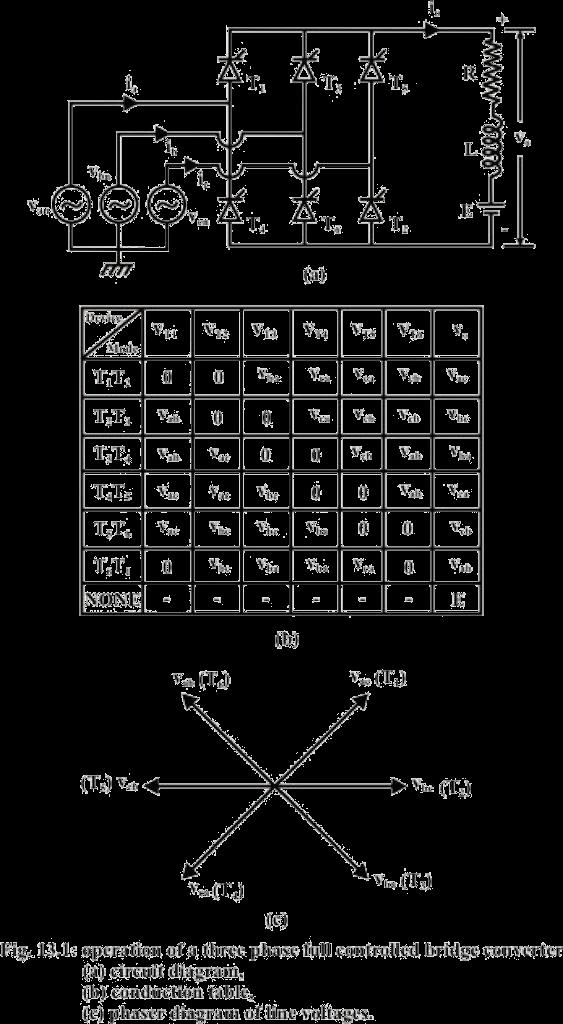
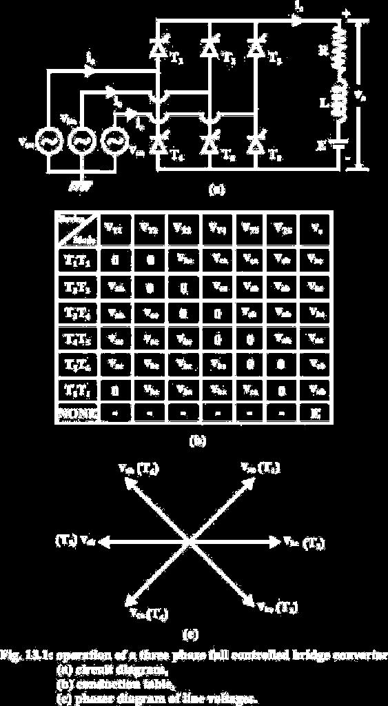
73 DEPARTMENT OF EEE SVECW Page 73
74 For any current to flow in the load at least one device from the top group (T 1, T 3, T 5 ) and one from the bottom group (T 2, T 4, T 6 ) must conduct. It can be argued as in the case of an uncontrolled converter only one device from these two groups will conduct. Then from symmetry consideration it can be argued that each thyristor conducts for 120 of the input cycle. Now the thyristors are fired in the sequence T 1 T 2 T 3 T 4 T 5 T 6 T 1 with 60 interval between each firing. Therefore thyristors on the same phase leg are fired at an interval of 180 and hence can not conduct simultaneously. This leaves only six possible conduction mode for the converter in the continuous conduction mode of operation. These are T 1 T 2, T 2 T 3, T 3 T 4, T 4 T 5, T 5 T 6, T 6 T 1. Each conduction mode is of 60 duration and appears in the sequence mentioned. The conduction table of Fig (b) shows voltage across different devices and the dc output voltage for each conduction interval. The phasor diagram of the line voltages appear in Fig (c). Each of these line voltages can be associated with the firing of a thyristor with the help of the conduction table-1. For example the thyristor T 1 is fired at the end of T 5 T 6 conduction interval. During this period the voltage across T 1 was v ac. Therefore T 1 is fired α angle after the positive going zero crossing of v ac. Similar observation can be made about other thyristors. The phasor diagram of Fig (c) also confirms that all the thyristors are fired in the correct sequence with 60 interval between each firing. Fig shows the waveforms of different variables (shown in Fig (a)). To arrive at the waveforms it is necessary to draw the conduction diagram which shows the interval of conduction for each thyristor and can be drawn with the help of the phasor diagram of fig (c). If the converter firing angle is α each thyristor is fired α angle after the positive going zero crossing of the line voltage with which it s firing is associated. Once the conduction diagram is drawn all other voltage waveforms can be drawn from the line voltage waveforms and from the conduction table of fig (b). Similarly line currents can be drawn from the output current and the conduction diagram. It is clear from the waveforms that output voltage and current waveforms are periodic over one sixth of the input cycle. Therefore this converter is also called the six pulse converter. The input current on the other hand contains only odds harmonics of the input frequency other than the triplex (3 rd, 9 th etc.) harmonics. The next section will analyze the operation of this converter in more details. DEPARTMENT OF EEE SVECW Page 74

75 DEPARTMENT OF EEE SVECW Page 75
76 5.3Analysis of the converter in the rectifier mode The output voltage waveform can be written as The input phase current i a is expressed as i a = i 0 α ω t α+ π 3 2π 4π i a = - i 0 α+ 3 ω t α+ 3 5π i a = i 0 α+ 3 ω t α+ 2π i a = 0 otherwise From Fig it can be observed that i 0 itself has a ripple at a frequency six times the input frequency. The closed from expression of i 0, as will be seen later is some what complicated. However, considerable simplification in the expression of i a can be obtained if i 0 is replaced by its average value I 0. This approximation will be valid provided the ripple on i 0 is small, i.e, the load is highly inductive. The modified input current waveform will then be i a which can be expressed in terms of a fourier series as To find out the condition for continuous conduction it is noted that in the limiting case of continuous conduction. i, Now if θ α+ then i0 is minimum at ωt = α. Condition min 0 =0 3 for continuous conduction is i 0 ωt=α 0. However discontinuous conduction is rare in these conversions and will not be discussed any further. 5.4 Analysis of the converter in the inverting mode. In all the analysis presented so far it has been assumed that α < 90. It follows from equation 13.2 that the output dc voltage will be positive in this case and power will be flowing from the three phase ac side to the dc side. This is the rectifier mode of operation of the converter. However if α is made larger than 90 the direction of power flow through the converter will reverse provided there exists a power source in the dc side of suitable polarity. The converter in that case is said to be operating in the inverter mode. It has been explained in connection with single phase converters that the polarity of EMF source on the dc side [Fig. 13.1(a)] would have to be reversed for inverter mode of operator. Fig shows the circuit connection and wave forms in the inverting mode of operation where the load current has been assumed to be continuous and ripple free. π DEPARTMENT OF EEE SVECW Page 76
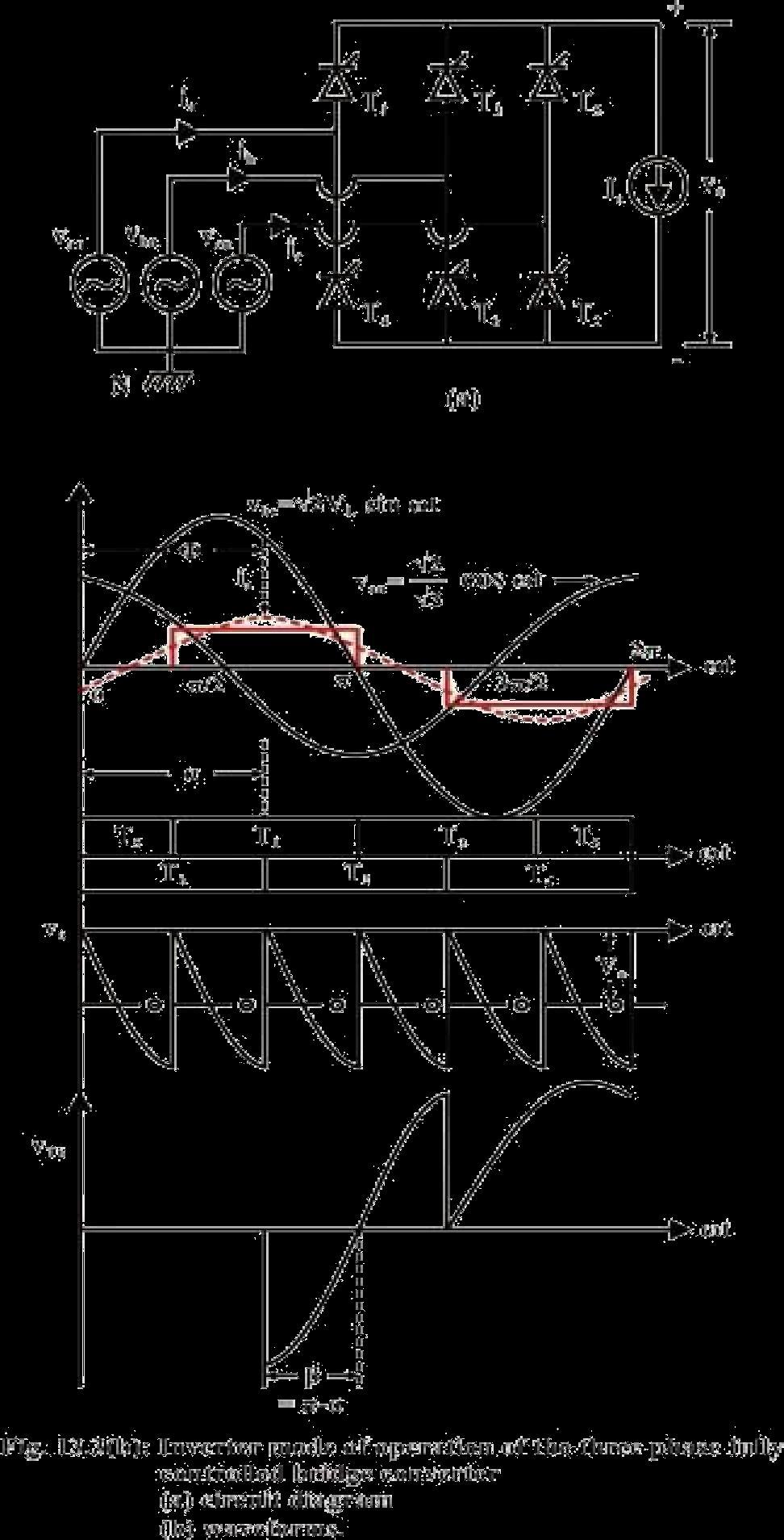
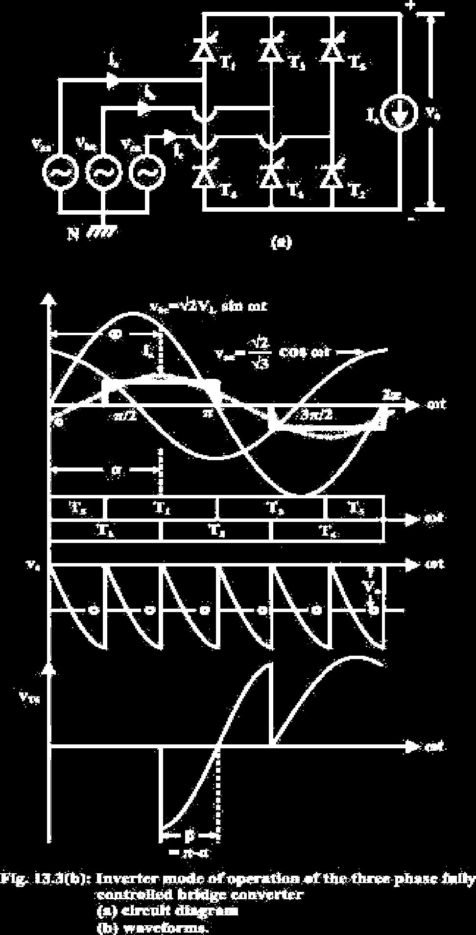
77 DEPARTMENT OF EEE SVECW Page 77
78 Analysis of the converter in the inverting mode is similar to its rectifier mode of operation. The same expressions hold for the dc and harmonic compounds in the output voltage and current. The input supply current Fourier series is also identical to Equation In particular 3 2 V = V cosα (13.24) 0 π L 2 3 i = I cos(ωt - α) (13.25) a 1 π 0 For values of α in the range 90 < α < 180 it is observed from Fig. 13.3(b) that the average dc voltage is negative and the displacement angle φ of the fundamental component of the input ac line current is equal to α > 90. Therefore, power in the ac side flows from the converter to the source. It is observed form Fig. 13.3(b) that an outgoing thyristor (thyristor T 6 in Fig. 13.3(b)) after commutation is impressed with a negative voltage of duration β = π α. For successful commutation of the outgoing thyristor it is essential that this interval is larger than the turn off time of the thyristor i.e, β ωtq, tq is the thyristor turn off time Therefore π- α ωtq or α π- ωtq. Which imposes an upper limit on the value of α. In practice this upper value of α is further reduced due to commutation overlap. Exercise 13.2 A three phase fully controlled bridge converter operating from a 3 phase 220 V, 50 Hz supply is used to charge a battery bank with nominal voltage of 240 V. The battery bank has an internal resistance of 0.01 Ω and the battery bank voltage varies by ± 10% around its nominal value between fully charged and uncharged condition. Assuming continuous conduction find out. - The range of firing angle of the converter. - The range of ac input power factor. - The range of charging efficiency. DEPARTMENT OF EEE SVECW Page 78
79 When the battery bank is charged with a constant average charging current of 100 Amps through a 250 mh lossless inductor. Answer: The maximum and minimum battery voltages are, V B Min = 0.9 V B Nom = 216 volts and V B Max = 1.1 V B Nom = 264 volts respectively. Since the average charging current is constant at 100 A. V 0 Max = V B Max R B = = 265 volts V 0 Min = V B Min R B = = 217 volts. 2. A three phase fully controlled converter operates from a 3 phase 230 V, 50 Hz supply through a Y/ transformer to supply a 220 V, 600 rpm, 500 A separately excited dc motor. The motor has an armature resistance of 0.02 Ω. What should be the transformer turns ratio such that the converter produces rated motor terminal voltage at 0º firing angle. Assume continuous conduction. The same converter is now used to brake the motor regeneratively in the reverse direction. If the thyristors are to be provided with a minimum turn off time of 100 μs, what is the maximum reverse speed at which rated braking torque can be produced. Answer: From the given question 3 2 VL = V V = 220 π L Where V L is the secondary side line and also the phase voltage since the secondary side is connected. Primary side phase voltage = 230 V = V 3 Turns ratio = =1: During regenerative braking in the reverse direction the converter operates in the inverting mode. tq Min =100μS β Min = ωtq Min =1.8 o 6 α Max = 180 β Min = 178.2º 7 Maximum negative voltage that can be generated by the converter is 3 π 2 VL cos o = V For rated braking torque I a = 500 A E b = V a I ar a = V. At 600 RPM E b = = 210 V. DEPARTMENT OF EEE SVECW Page 79
80 Max reverse speed is = RPM Higher pulse number converters and dual converter The three phase fully controlled converter is widely used in the medium to moderately high power applications. However in very large power applications (such as HV DC transmission systems) the device ratings become impractically large. Also the relatively low frequency (6 th in the dc side, 5 th and 7 th in the ac side) harmonic voltages and currents produced by this converter become unacceptable. Therefore several such converters are connected in series parallel combination in order to increase the voltage / current rating of the resulting converter. Furthermore if the component converters are controlled properly some lower order harmonics can be eliminated both from the input and output resulting in a higher pulse converter. DEPARTMENT OF EEE SVECW Page 80
81 Fig. 13.4(a) schematically represents series connection of two six pulse converters where as Fig. 13.4(b) can be considered to be a parallel connection. The inductance in between the converters has been included to limit circulating harmonic current. In both these figures CONV I and CONV II have identical construction and are also fired at the same firing angle α. Their input supplies also have same magnitude but displaced in phase by an angle φ. Then one can write Now if cos 3Kφ = 0 for some K then the corresponding harmonic disappear from the fourier series expression of v 0. In particular if φ = 30 then cos 3Kφ = 0 for K = 1, 2, 3, 5. This phase difference can be obtained by the arrangement shown in Fig. 13.4(c). Then It can be seen that the frequency of the harmonics present in the output voltage has the form 12ω, 24ω, 36ω.. Similarly it can be shown that the input side line current i ABC have harmonic frequency of the form 11ω, 13ω, 23ω, 25ω, 35ω, 37ω,. Which is the characteristic of a 12 pulse converter. In a similar manner more number of 3 phase 6 pulse converters can be connected in series / parallel and the φ angle can be adjusted to obtain 18 and 24 pulse converters. One of the shortcomings of a three phase fully controlled converter is that although it can produce both positive and negative voltage it can not supply current in both directions. However, some applications such as a four quadrant dc motor drive require this capability from the dc source. This problem is easily mitigated by connecting another three phase fully controlled converter in anti parallel as shown in Fig (a). In this figure converter -I supplies positive load current while converter-ii supplies negative load current. In other words converter-i operates in the first and fourth quadrant of the output v i plane whereas converter-ii operates in the third and fourth quadrant. Thus the two converters taken together can operate in all four quadrants and is capable of supplying a four quadrant dc motor drive. The combined converter is called the Dual converter. DEPARTMENT OF EEE SVECW Page 81

82 DEPARTMENT OF EEE SVECW Page 82
83 Obviously since converter-i and converter-ii are connected in antiparallel they must produce the same dc voltage. This requires that the firing angles of these two converters be related as α 2 = π α 1 (13.30) Although Equations ensures that the dc voltages produced by these converters are equal the output voltages do not match on an instantaneous basis. Therefore to avoid a direct short circuit between two different supply lines the two converters must never be gated simultaneously. Converter-I receives gate pulses when the load current is positive. Gate pulses to converter-ii are blocked at that time. For negative load current converter-ii thyristors are fired while converter-i gate pulses are blocked. Thus there is no circulating current flowing through the converters and therefore it is called the non-circulating current type dual converter. It requires precise sensing of the zero crossing of the output current which may pose a problem particularly at light load due to possible discontinuous conduction. To overcome this problem an interphase reactor may be incorporated between the two converters. With the interphase reactor in place both the converters can be gated simultaneously with α 2 = π α 1. The resulting converter is called the circulating current type dual converter Gate Drive circuit for three phase fully controlled converter Several schemes exist to generate gate drive pulses for single phase or three phase converters. In many application it is required that the output of the converter be proportional to a control voltage. This can be achieved as follows. The following circuit can be used to generate α according to equation DEPARTMENT OF EEE SVECW Page 83
 is compared with v c. The firing pulse is generated at the point when these two waveforms are equal.")

84 In the circuit of Fig. 13.6(a) a phase shift network is used to obtain a waveform leading v i by 90º. The phasor diagram of the phase shift circuit is shown in Fig. 13.6(b). The output of the phase shift waveform (and its inverse) is compared with v c. The firing pulse is generated at the point when these two waveforms are equal. Obviously at-this instant Therefore this method of generation of converter firing pulses is called inverse cosine control. The output of the phase shift network is called carrier waveform. Similar technique can be used for three phase converters. However the phase shift network here consists of a three phase signal transformer with special connections as shown in Fig DEPARTMENT OF EEE SVECW Page 84
 T 2 is fired α angle after the positive going zero crossing of v bc. Therefore, to implement inverse cosine the carrier wave for T 2 must lead v bc by 90º.")
85 The signal transformer uses three single phase transformer each of which has two secondary windings. The primary windings are connected in delta while the secondary windings are connected in zigzag. From Fig (c) T 2 is fired α angle after the positive going zero crossing of v bc. Therefore, to implement inverse cosine the carrier wave for T 2 must lead v bc by 90º. This waveform is obtained from zigzag connection of the winding segments a 1 a 2 and c 1 c 2 as shown in Fig. 13.7(a). The same figure also shows the zigzag connection for other phase. The voltage across each zigzag phase can be used to fire two thyristors belonging to the same phase leg using a circuit similar to Fig (a). The phase shift network will not be required in this case. DEPARTMENT OF EEE SVECW Page 85
86 Exercise Fill in the blank(s) with the appropriate word(s) i) Higher pulse number converters can be realized by and connection of six pulse converters. ii) Constituent six pulse converters of a 12 pulse converter have firing angles. iii) The input supply voltages to the converters of a 12 pulse converter have magnitudes and are phase shifted from one another by degrees. iv) The input supply to a 12 pulse converter can be obtained through a connected transformer. v) Dual converters are used for supplying quadrant dc motor drives. vi) In a dual converter if one converter is fired at an angle α the other has to be fired at. vii) In current dual converter only one converter conducts t any time. viii) In a circulating current type dual converter an is used between the converters to limit the circulating current. ix) To obtain a linear control relation between the control voltage and the output dc voltage of a converter control logic is used. x) In a three phase fully controlled converter the carrier waves for firing pulse generation are obtained using three connected single phase transformers. Answers: (i) Series, parallel; (ii) same, (iii) equal, 30, (iv) star star delta; (v) four; (vi) π - α, (vii) non-circulating ; (viii) inductor, (ix) inverse-cosine; (x) delta-zigzag. 3. What will happen if the signal transformers generating the carrier wave have delta double star connection instead of delta-zigzag connection. Answer: With delta-double star connection of the signal transformers the carrier wave forms will be in phase with the line voltage waveforms. Therefore, without a phase shift network it will not be possible to generate carrier waveforms which are in quadrature with the line voltages. Hence inverse casine control law cannot be implemented. Summary A three phase fully controlled converter is realized by replacing the diodes of an uncontrolled converter with thyristors. A three phase fully controlled converter can operate either as a rectifier or as an inverter. The output voltage of a three phase fully controlled converter contains multiple of sixth DEPARTMENT OF EEE SVECW Page 86
87 harmonic of the input frequency in addition to the dc component. The input current of a three phase fully controlled converter contains only odd harmonics other than tripler harmonics. The input current displacement factor of a three phase fully controlled converter is cos α. α being the firing angle. In the continuous conduction mode a three phase fully controlled converter may operate in the inverting mode by increasing α beyond 90º. In the inverting mode the firing angle should be less than 180º for safe commutation of the thyristors. Several units of three phase fully controlled converters can be connected in series parallel to form higher pulse number (12, 18, 24 etc) converters. In higher pulse number converters all component converters are fired at the same firing angle while their input supplies are phase shifted from one another by a predetermined angle. Two three phase fully controlled converter can be connected in anti parallel to form a dual converter which can operate in all four quadrants of the V-I plane. Dual converters can be of circulating and non circulating current type. Fully controlled converters employ inverse casine control strategy for generating firing pulses which gives linear relationship between the output voltage and the control voltage. In a three phase fully controlled converter, a three phase delta/zig-zag connected signal transformer is used to generate the required carrier waves for this purpose. DEPARTMENT OF EEE SVECW Page 87
88 UNIT-VI AC VOLTAGE CONTROLLERS & CYCLO CONVERTERS DEPARTMENT OF EEE SVECW Page 88
89 6.1Cycloconverters In Figs. 3.2 and 3.3, the two typical types of cycloconverters are presented. In the first case there are two three-phase midpoint controlled rectifiers connected back to back. The second case shows two three-phase bridge rectifier converters connected back to back. Both are used for three-phase to three-phase conversion. In Fig. 3.4 the single-phase output voltage and current waves are presented for the Frequency converters AC-AC Converters (direct frequency converters) AC-DC- AC Converter s Cycloconverters Matrix converters FIGURE 3.1 Classification of frequency converters. R S T ~V ; 60 Hz p convert er n converter a i a b c LOAD FIGURE 3.2 Cycloconverter scheme with three-phase midpoint controlled rectifier. DEPARTMENT OF EEE SVECW Page 89
90 R S T Transformer p convert er n convert er i a a b c LOAD FIGURE 3.3 Cycloconverter scheme with three-phase bridge controlled rectifier. bridge rectifier circuits. The output voltage V a and current i a have V a 1 and i a1 fundamental components with φ 1 phase displacement and numerous harmonics. Because of the load inductance, the current harmonics will be significantly lower than the voltage harmonics. The firing angles are α P and α N for the p and n converters, respectively. In general, the controls are designed so that only the thyristors of either the p or n converter is firing, which produces a current in the desired direction. During this period the other converter is blocked. When the current changes direction, both converters must be blocked for a short time. It is possible to operate without blocking the converters. In this case, their average voltage must be the same, and therefore the relation αp αn is valid. However, additional inductances are necessary to limit the circulating currents between two converters since the instantaneous voltages of the two converters differ from one another. DEPARTMENT OF EEE SVECW Page 90
91 V V Va a 1 ω 1 t α n i φ1 ia i a1 ω 1 t n p and n blocked p inve inverte rter p rectifier r p and n n blocked rectifier p n block blocked ed FIGURE 3.4 Voltage and current vs. time for cycloconverter with three-phase bridge converters. Nine independent bidirectional switches R a Load (60 S (variable HZ) b voltage and variable frequenc y) T c FIGURE 3.5 Three-phase to three-phase matrix converter. DEPARTMENT OF EEE SVECW Page 91
92 The phase control of the p and n converters is modulated by a sine or trapezoidal wave. The content of the harmonics for sine modulation is lower; however, the maximum value of the output voltage is lower than that for trapezoidal modulation. During every cycle of the output voltage both of the converters must work as rectifiers and inverters. The shape of the output voltage goes from bad to worse with an increase in the output voltage and the output frequency. If the frequency reaches the well-defined value the current harmonics become unacceptable. This frequency is usually 33% of supply frequency for three-phase midpoint ( Fig. 3.2) and 50% for three-phase bridge ( Fig. 3.3) converters. The cycloconverter is usually used for three-phase, high-power, low-speed synchronous motor drives and rarely employed for induction motor drives. 6.2 AC VOLTAGE CONTROLLERS 6.1 Introduction AC to AC voltage converters operates on the AC mains essentially to regulate the output voltage. Portions of the supply sinusoid appear at the load while the semiconductor switches block the remaining portions. Several topologies have emerged along with voltage regulation methods, most of which are linked to the development of the semiconductor devices. Fig 26.1 Some single phase AC-AC voltage regulator topologies. (a) Back-to -back SCR; (b) One SCR in (a) replaced by a four-diode full wave diode bridge; (c) A bi-directionally conducting TRIAC; (d) The SCR in (b) replaced by a transistor. DEPARTMENT OF EEE SVECW Page 92
93 The regulators in Fig 26.1 (a), (b) and (c) perform quite similarly. They are called Phase Angle Controlled (PAC) AC-AC converters or AC-AC choppers. The TRIAC based converter may be considered as the basic topology. Being bi-directionally conducting devices, they act on both polarities of the applied voltage. However, dv dt re applied their ratings being poor, they tend to turn-on in the opposite direction just subsequent to their turn-off with an inductive load. The 'Alternistor' was developed with improved features but was not popular. The TRIAC is common only at the low power ranges. The (a) and (b) options are improvements on (c) mostly regarding current handling and turn-off-able current rating. A transistorised AC-AC regulator is a PWM regulator similar to the DC-DC converters. It also requires a freewheeling path across the inductive load, which has also got to be bidirectional. Consequently, only controlled freewheeling devices can be used Operation with resistive loads Fig illustrates the operation of the PAC converter with a resistive load. The device(s) is triggered at a phase-angle 'α' in each cycle. The current follows the voltage wave shape in each half and extinguishes itself at the zero crossings of the supply voltage. In the two-scr topology, one SCR is positively biased in each half of the supply voltage. There is no scope for conduction overlap of the devices. A single pulse is sufficient to trigger the controlled devices with a resistive load. In the diode-scr topology, two diodes are forward biased in each half. The SCR always receives a DC voltage and does not distinguish the polarity of the supply. It is thus always forward biased. The bi-directional TRIAC is also forward biased for both polarities of the supply voltage. DEPARTMENT OF EEE Page 93
94 Fig Operation of a Phase Angle Controlled AC-AC converter with a resistive load Fig The rms output voltage and the most important harmonics versus triggering angle α. As is evident from the current waveforms, the PAC introduces significant harmonics both into the load and the supply. This is one of the main reasons why such controllers are today not acceptable. The ideal waveform as shown in Fig 26.2 is half wave symmetric. However it is to be achieved by the trigger circuits. The controller in Fig ensures this for the TRIAC based circuit. While the TRIAC has a differing characteristic for the two polarities of biasing with the 32V DIAC - a two terminal device- triggering is effected when the capacitor voltage reaches 32 V. This ensures elimination of DC and even components in the output voltage. Fig DIAC based trigger circuit for a TRIAC to ensure symmetrical triggering in the two halves of the supply. For the SCR based controllers, identical comparators for the two halves of the AC supply, which generates pulses for the two SCRs ensures DC and even harmonic free operation. The PAC operates with a resistive load for all values of α ranging from 0 o The fundamental current, i f can be represented as DEPARTMENT OF EEE Page 94

95 In machine drives it is only the fundamental component, which is useful. However, in resistance heating type of application all harmonics are of no consequence. The corrupted supply current nevertheless is undesirable. 6.3 Power Factor The power factor of a nonlinear deserves a special discussion. Fig shows the supply voltage and the non-sinusoidal load current. The fundamental load/supply current lags the supply voltage by the φ1, 'Fundamental Power Factor' angle. Cosφ1 is also called the 'Displacement Factor'. However this does not account for the total reactive power drawn by the system. This power factor is inspite of the actual load being resistive! The reactive power is drawn also y the trigger-angle dependent harmonics. Now The portion within square brackets in Eq is identical to the first part of the expression within brackets in Eq. 26.1, which is called the Fourier coefficient 'B 1 B'. The rms load voltage can also be similarly obtained by integrating between α and π and the result can be combined with Eq to give power factor = per unit rms load current = per unit load power = B p.u.. 1 Fig Variation of various performance parameters with triggering angle DEPARTMENT OF EEE Page 95

96 6.4 Operation with inductive loads With inductive loads the operation of the PAC is illustrated in Fig The current builds up from zero in each cycle. It quenches not at the zero crossing of the applied voltage as with the resistive load but after that instant. The supply voltage thus continues to be impressed on the load till the load current returns to zero. A single-pulse trigger for the TRIAC 26.1 (c) or the antiparallel SCR (b) has no effect on the devices if it (or the anti-parallel device) is already in conduction in the reverse direction. The devices would fail to conduct when they are intended to, as they do not have the supply voltage forward biasing them when the trigger pulse arrives. A single pulse trigger will work till the trigger angle α > φ, where φ is the power factor angle of the inductive load. A train of pulses is required here. The output voltage is controllable only between triggering angles φ and 180 o. The load current waveform is further explained in Fig The current is composed of two components. The first is the steady state component of the load current, i ss and the second, i tr is the transient component. Fig Operation of a single phase PAC with an inductive load Fig 26.7 Load current for a single phase AC-AC converter with a R_L load. V s - supply voltage, i ss -steady state current component, i tr - transient current component and i load - load current (= i ss + i tr ). DEPARTMENT OF EEE Page 96

97 With an inductance in the load the distinguishing feature of the load current is that it must always start from zero. However, if the switch could have permanently kept the load connected to the supply the current would have become a sinusoidal one phase shifted from the voltage by the phase angle of the load, φ. This current restricted to the half periods of conduction is called the 'steady-state component' of load current i ss. The 'transient component' of load current i tr, again in each half cycle, must add up to zero with this i ss to start from zero. This condition sets the initial value of the transient component to that of the steady state at the instant that the SCR/TRIAC is triggered. Fig illustrates these relations. When a device is in conduction, the load current is governed by the equation L di dt + Ri =v s i load R (α ω t ) = 2V [ sin (ω t φ)+ sin (α φ)e L ] Z Since at t = 0, i load = 0 and supply voltage v s = 2Vsinωt the solution is of the form The instant when the load current extinguishes is called the extinction angle β. It can be inferred that there would be no transients in the load current if the devices are triggered at the power factor angle of the load. The load current I that case is perfectly sinusoidal AC-AC Chopper Fig A complete Transitorised AC-AC chopper topology of the version shown in Fig and the corresponding load voltage and current waveforms for an inductive load. The output voltage is shown to be about 50% for a 0.5 Duty Ratio chopping. The AC-AC converter shown in Fig 26.1 has to be augmented with two additional controlled devices clamping the load as indicated in Fig A large capacitor across the supply terminals is also to be inserted. These devices which are mostly transistors of the same variety as used for the chopper are necessary to clamp the voltages generated by the switching-off of the current carrying inductors in the load while the input capacitor takes care of the line inductances. The harmonics in the line current and load voltage waveforms are significantly different from those with the PACs. Mostly switching frequency harmonics are present in both the waveforms. DEPARTMENT OF EEE Page 97
98 6.5 PAC as a static switch Both single phase and three phase PACs are often used as static switches for applications like switching on of highly inductive loads without transients or for regulating output AC voltages by switching in tapings of a transformer. Such sequence control PACs while controlling the output voltage also permit improvement of the power factor as seen by the source. Sequence control can be two or multiple phase depending upon the application. Typical load voltage and current waveforms are shown in Fig The outer TRIACs connected to thwe higher voltage leads of the input transformer are triffered at the desired angle α, to realize the required load voltage. Obviously this voltage is greater than that available at the low voltage terminal of the transformer. This device continues conduction into the next half of the supply voltage till the load current falls to zero. The inner TR 2 starts conduction subsequently, requiring a wide pulse or a train of pulses. TR 1 can be however triggered by a single pulse. Fig Load voltage and current control with a two-stage sequence control Practice Questions and Problems with Answers Q1 A single-phase transformer, assumed to have a negligible resistance compared to its inductance is switched on via a PAC. At what trigger angle will the operation be free from transients? A1 For the transformer load φ L 90 ο Therefore for transient free operation α = 90 ο Q2 For the load described in Q1, the PAC is triggered by a single pulse at α = 60 ο. Sketch the load current waveform. DEPARTMENT OF EEE Page 98

99 A2 Since α < φ L, the load current should have been continuous. However, the current in the SCR first triggered extinguishes at a β the total load current, i L = i ss + i tr = 0. For this load which can be considered to be highly inductive β 360 ο, say 360 ο. Thus the first SCR conducts till that angle. The anti-parallel SCR is triggered at α = 60 ο corresponding to a β = 240 ο when it is still reverse biased. It fails to conduct. The load thus sees only a unipolar current. The load current and voltage waveforms are illustrated in Fig 26. A2. Note that both the load voltage and current waveforms contain DC components. Fig. 26. A2 The load current waveform and its steady-state and transient components when a highly inductive load is switched using single narrow trigger pulses. DEPARTMENT OF EEE Page 99
Bridge Course On POWER ELECTRONICS
 G. PULLAIAH COLLEGE OF ENGINEERING AND TECHNOLOGY Accredited by NAAC with A Grade of UGC, Approved by AICTE, New Delhi Permanently Affiliated to JNTUA, Ananthapuramu (Recognized by UGC under 2(f) and 12(B)
Power Semiconductor Devices
 TRADEMARK OF INNOVATION Power Semiconductor Devices Introduction This technical article is dedicated to the review of the following power electronics devices which act as solid-state switches in the circuits.
Electrical Engineering EE / EEE. Postal Correspondence Course. Power Electronics. GATE, IES & PSUs
 Power Electronics-EE GATE, IES, PSU 1 SAMPLE STUDY MATERIAL Electrical Engineering EE / EEE Postal Correspondence Course Power Electronics GATE, IES & PSUs Power Electronics-EE GATE, IES, PSU 2 C O N T
UNIT I POWER SEMICONDUCTOR DEVICES. Ref signal Control Digital Power Load Circuit Circuit Electronic circuit. Feedback Signal
 UNIT I POWER SEMICONDUCTOR DEICES The control of electric motor drives requires control of electric power. Power electronics have eased the concept of power control. Power electronics signifies the word
FIELD EFFECT TRANSISTOR (FET) 1. JUNCTION FIELD EFFECT TRANSISTOR (JFET)
 1. JUNCTION FIELD EFFECT TRANSISTOR (JFET)") FIELD EFFECT TRANSISTOR (FET) The field-effect transistor (FET) is a three-terminal device used for a variety of applications that match, to a large extent, those of the BJT transistor. Although there
FIELD EFFECT TRANSISTOR (FET) The field-effect transistor (FET) is a three-terminal device used for a variety of applications that match, to a large extent, those of the BJT transistor. Although there
UNIT 3: FIELD EFFECT TRANSISTORS
 FIELD EFFECT TRANSISTOR: UNIT 3: FIELD EFFECT TRANSISTORS The field effect transistor is a semiconductor device, which depends for its operation on the control of current by an electric field. There are
Analog and Telecommunication Electronics
 Politecnico di Torino - ICT School Analog and Telecommunication Electronics F2 Active power devices»mos»bjt» IGBT, TRIAC» Safe Operating Area» Thermal analysis 30/05/2012-1 ATLCE - F2-2011 DDC Lesson F2:
2 Marks - Question Bank. Unit 1- INTRODUCTION
 Two marks 1. What is power electronics? EE6503 POWER ELECTRONICS 2 Marks - Question Bank Unit 1- INTRODUCTION Power electronics is a subject that concerns the applications electronics principles into situations
DOWNLOAD PDF POWER ELECTRONICS DEVICES DRIVERS AND APPLICATIONS
 Chapter 1 : Power Electronics Devices, Drivers, Applications, and Passive theinnatdunvilla.com - Google D Download Power Electronics: Devices, Drivers and Applications By B.W. Williams - Provides a wide
Solid State Devices- Part- II. Module- IV
 Solid State Devices- Part- II Module- IV MOS Capacitor Two terminal MOS device MOS = Metal- Oxide- Semiconductor MOS capacitor - the heart of the MOSFET The MOS capacitor is used to induce charge at the
Chapter 1 Power Electronic Devices
 Chapter 1 Power Electronic Devices Outline 1.1 An introductory overview of power electronic devices 1.2 Uncontrolled device power diode 1.3 Half- controlled device thyristor 1.4 Typical fully- controlled
SRM INSTITUTE OF SCIENCE AND TECHNOLOGY (DEEMED UNIVERSITY)
") SRM INSTITUTE OF SCIENCE AND TECHNOLOGY (DEEMED UNIVERSITY) QUESTION BANK I YEAR B.Tech (II Semester) ELECTRONIC DEVICES (COMMON FOR EC102, EE104, IC108, BM106) UNIT-I PART-A 1. What are intrinsic and
SRM INSTITUTE OF SCIENCE AND TECHNOLOGY (DEEMED UNIVERSITY) QUESTION BANK I YEAR B.Tech (II Semester) ELECTRONIC DEVICES (COMMON FOR EC102, EE104, IC108, BM106) UNIT-I PART-A 1. What are intrinsic and
FET(Field Effect Transistor)
") Field Effect Transistor: Construction and Characteristic of JFETs. Transfer Characteristic. CS,CD,CG amplifier and analysis of CS amplifier MOSFET (Depletion and Enhancement) Type, Transfer Characteristic,
Field Effect Transistor: Construction and Characteristic of JFETs. Transfer Characteristic. CS,CD,CG amplifier and analysis of CS amplifier MOSFET (Depletion and Enhancement) Type, Transfer Characteristic,
UNIT-VI FIELD EFFECT TRANSISTOR. 1. Explain about the Field Effect Transistor and also mention types of FET s.
 UNIT-I FIELD EFFECT TRANSISTOR 1. Explain about the Field Effect Transistor and also mention types of FET s. The Field Effect Transistor, or simply FET however, uses the voltage that is applied to their
Lecture 3: Transistors
 Lecture 3: Transistors Now that we know about diodes, let s put two of them together, as follows: collector base emitter n p n moderately doped lightly doped, and very thin heavily doped At first glance,
UNIT I POWER SEMI-CONDUCTOR DEVICES
 UNIT I POWER SEMI-CONDUCTOR DEVICES SUBJECT CODE SUBJECT NAME STAFF NAME : EE6503 : Power Electronics : Ms.M.Uma Maheswari 1 SEMICONDUCTOR DEVICES POWER DIODE POWER TRANSISTORS POWER BJT POWER MOSFET IGBT
UNIT II JFET, MOSFET, SCR & UJT
 UNIT II JFET, MOSFET, SCR & UJT JFET JFET as an Amplifier and its Output Characteristics JFET Applications MOSFET Working Principles, SCR Equivalent Circuit and V-I Characteristics. SCR as a Half wave
Power Electronics Power semiconductor devices. Dr. Firas Obeidat
 Power Electronics Power semiconductor devices Dr. Firas Obeidat 1 Table of contents 1 Introduction 2 Classifications of Power Switches 3 Power Diodes 4 Thyristors (SCRs) 5 The Triac 6 The Gate Turn-Off
Field Effect Transistors (npn)
") Field Effect Transistors (npn) gate drain source FET 3 terminal device channel e - current from source to drain controlled by the electric field generated by the gate base collector emitter BJT 3 terminal
Field Effect Transistors (npn) gate drain source FET 3 terminal device channel e - current from source to drain controlled by the electric field generated by the gate base collector emitter BJT 3 terminal
UNIVERSITY OF TECHNOLOGY
 UNIVERSITY OF TECHNOLOGY Third Year DEPARTMENT OF ELECTRICAL ENGINEERING Electronics Engineering Section AC Machine and Power Electronics 2016-2017 Module-II: Power Electronics: Power electronics devices
MTLE-6120: Advanced Electronic Properties of Materials. Semiconductor transistors for logic and memory. Reading: Kasap
 MTLE-6120: Advanced Electronic Properties of Materials 1 Semiconductor transistors for logic and memory Reading: Kasap 6.6-6.8 Vacuum tube diodes 2 Thermionic emission from cathode Electrons collected
UNIT 3 Transistors JFET
 UNIT 3 Transistors JFET Mosfet Definition of BJT A bipolar junction transistor is a three terminal semiconductor device consisting of two p-n junctions which is able to amplify or magnify a signal. It
Analog Electronics. Electronic Devices, 9th edition Thomas L. Floyd Pearson Education. Upper Saddle River, NJ, All rights reserved.
 Analog Electronics BJT Structure The BJT has three regions called the emitter, base, and collector. Between the regions are junctions as indicated. The base is a thin lightly doped region compared to the
Switching and Semiconductor Switches
 1 Switching and Semiconductor Switches 1.1 POWER FLOW CONTROL BY SWITCHES The flow of electrical energy between a fixed voltage supply and a load is often controlled by interposing a controller, as shown
SCR- SILICON CONTROLLED RECTIFIER
 SCR- SILICON CONTROLLED RECTIFIER Definition: When a pn junction is added to a junction transistor, the resulting three pn junction device is called a silicon controlled rectifier. SCR can change alternating
SYED AMMAL ENGINEERING COLLEGE
 SYED AMMAL ENGINEERING COLLEGE (Approved by the AICTE, New Delhi, Govt. of Tamilnadu and Affiliated to Anna University, Chennai) Established in 1998 - An ISO 9001:2008 Certified Institution Dr. E.M.Abdullah
Questions on JFET: 1) Which of the following component is a unipolar device?
 Which of the following component is a unipolar device?") Questions on JFET: 1) Which of the following component is a unipolar device? a) BJT b) FET c) DJT d) EFT 2) Current Conduction in FET takes place due e) Majority charge carriers only f) Minority charge
Questions on JFET: 1) Which of the following component is a unipolar device? a) BJT b) FET c) DJT d) EFT 2) Current Conduction in FET takes place due e) Majority charge carriers only f) Minority charge
Prof. Steven S. Saliterman Introductory Medical Device Prototyping
 Introductory Medical Device Prototyping Department of Biomedical Engineering, University of Minnesota http://saliterman.umn.edu/ Solid state power switching: Silicon controlled rectifiers (SCR or Thyristor).
QUESTION BANK EC6201 ELECTRONIC DEVICES UNIT I SEMICONDUCTOR DIODE PART A. It has two types. 1. Intrinsic semiconductor 2. Extrinsic semiconductor.
 FATIMA MICHAEL COLLEGE OF ENGINEERING & TECHNOLOGY Senkottai Village, Madurai Sivagangai Main Road, Madurai - 625 020. [An ISO 9001:2008 Certified Institution] QUESTION BANK EC6201 ELECTRONIC DEVICES SEMESTER:
Experiment (1) Principles of Switching
 Principles of Switching") Experiment (1) Principles of Switching Introduction When you use microcontrollers, sometimes you need to control devices that requires more electrical current than a microcontroller can supply; for this,
Experiment (1) Principles of Switching Introduction When you use microcontrollers, sometimes you need to control devices that requires more electrical current than a microcontroller can supply; for this,
ELG4139: Power Electronics Systems Objective To Realize and Design Various Power Supplies and Motor Drives!
 ELG4139: Power Electronics Systems Objective To Realize and Design Various Power Supplies and Motor Drives! Power electronics refers to control and conversion of electrical power by power semiconductor
Reg. No. : Question Paper Code : B.E./B.Tech. DEGREE EXAMINATION, NOVEMBER/DECEMBER Second Semester
 WK 5 Reg. No. : Question Paper Code : 27184 B.E./B.Tech. DEGREE EXAMINATION, NOVEMBER/DECEMBER 2015. Time : Three hours Second Semester Electronics and Communication Engineering EC 6201 ELECTRONIC DEVICES
I E I C since I B is very small
 Figure 2: Symbols and nomenclature of a (a) npn and (b) pnp transistor. The BJT consists of three regions, emitter, base, and collector. The emitter and collector are usually of one type of doping, while
Unit III FET and its Applications. 2 Marks Questions and Answers
 Unit III FET and its Applications 2 Marks Questions and Answers 1. Why do you call FET as field effect transistor? The name field effect is derived from the fact that the current is controlled by an electric
Power semiconductors. José M. Cámara V 1.0
 Power semiconductors José M. Cámara V 1.0 Introduction Here we are going to study semiconductor devices used in power electronics. They work under medium and high currents and voltages. Some of them only
SUMMER 13 EXAMINATION Subject Code: Model Answer Page No: / N
 Important Instructions to examiners: 1) The answers should be examined by key words and not as word-to-word as given in the model answer scheme. 2) The model answer and the answer written by candidate
ELG3336: Power Electronics Systems Objective To Realize and Design Various Power Supplies and Motor Drives!
 ELG3336: Power Electronics Systems Objective To Realize and Design arious Power Supplies and Motor Drives! Power electronics refers to control and conversion of electrical power by power semiconductor
INTRODUCTION: Basic operating principle of a MOSFET:
 INTRODUCTION: Along with the Junction Field Effect Transistor (JFET), there is another type of Field Effect Transistor available whose Gate input is electrically insulated from the main current carrying
4.2.2 Metal Oxide Semiconductor Field Effect Transistor (MOSFET)
") 4.2.2 Metal Oxide Semiconductor Field Effect Transistor (MOSFET) The Metal Oxide Semitonductor Field Effect Transistor (MOSFET) has two modes of operation, the depletion mode, and the enhancement mode.
4.2.2 Metal Oxide Semiconductor Field Effect Transistor (MOSFET) The Metal Oxide Semitonductor Field Effect Transistor (MOSFET) has two modes of operation, the depletion mode, and the enhancement mode.
6. Field-Effect Transistor
 6. Outline: Introduction to three types of FET: JFET MOSFET & CMOS MESFET Constructions, Characteristics & Transfer curves of: JFET & MOSFET Introduction The field-effect transistor (FET) is a threeterminal
POWER ELECTRONICS POWER ELECTRONICS INTRODUCTION TO. Dr. Adel Gastli. CONTENTS
 POWER ELECTRONICS INTRODUCTION TO POWER ELECTRONICS Dr. Adel Gastli Email: adel@gastli.net http://adel.gastli.net CONTENTS 1. Definitions and History 2. Applications of Power Electronics 3. Power Semiconductor
3. Draw the two transistor model of a SCR and mention its applications. (MAY 2016)
") DHANALAKSHMI COLLEGE OF ENGINEERING DEPARTMENT OF ELECTRICAL AND ELECTRONICS ENGINEERING EE6503 POWER ELECTRONICS UNIT I- POWER SEMI-CONDUCTOR DEVICES PART - A 1. What is a SCR? A silicon-controlled rectifier
DHANALAKSHMI COLLEGE OF ENGINEERING DEPARTMENT OF ELECTRICAL AND ELECTRONICS ENGINEERING EE6503 POWER ELECTRONICS UNIT I- POWER SEMI-CONDUCTOR DEVICES PART - A 1. What is a SCR? A silicon-controlled rectifier
Basic Electronics Prof. Dr. Chitralekha Mahanta Department of Electronics and Communication Engineering Indian Institute of Technology, Guwahati
 Basic Electronics Prof. Dr. Chitralekha Mahanta Department of Electronics and Communication Engineering Indian Institute of Technology, Guwahati Module: 3 Field Effect Transistors Lecture-7 High Frequency
Module 04.(B1) Electronic Fundamentals
 Electronic Fundamentals") 1.1a. Semiconductors - Diodes. Module 04.(B1) Electronic Fundamentals Question Number. 1. What gives the colour of an LED?. Option A. The active element. Option B. The plastic it is encased in. Option
1.1a. Semiconductors - Diodes. Module 04.(B1) Electronic Fundamentals Question Number. 1. What gives the colour of an LED?. Option A. The active element. Option B. The plastic it is encased in. Option
BREAKDOWN DEVICES. Learning Objectives
 C H A P T E R64 Learning Objectives What are Breakdown Devices? Unijunction Transistor UJT Relaxation Oscillator Programmable UJT(PUT) Silicon Controlled Rectifier Comparison between Transistors and Thyristors
MODULE-2: Field Effect Transistors (FET)
") FORMAT-1B Definition: MODULE-2: Field Effect Transistors (FET) FET is a three terminal electronic device used for variety of applications that match with BJT. In FET, an electric field is established by
FORMAT-1B Definition: MODULE-2: Field Effect Transistors (FET) FET is a three terminal electronic device used for variety of applications that match with BJT. In FET, an electric field is established by
Scheme Q.1 Attempt any SIX of following: 12-Total Marks a) Draw symbol NPN and PNP transistor. 2 M Ans: Symbol Of NPN and PNP BJT (1M each)
 Draw symbol NPN and PNP transistor. 2 M Ans: Symbol Of NPN and PNP BJT (1M each)") Q. No. WINTER 16 EXAMINATION (Subject Code: 17319) Model Answer Important Instructions to examiners: 1) The answers should be examined by key words and not as word-to-word as given in the model answer
Q. No. WINTER 16 EXAMINATION (Subject Code: 17319) Model Answer Important Instructions to examiners: 1) The answers should be examined by key words and not as word-to-word as given in the model answer
Difference between BJTs and FETs. Junction Field Effect Transistors (JFET)
") Difference between BJTs and FETs Transistors can be categorized according to their structure, and two of the more commonly known transistor structures, are the BJT and FET. The comparison between BJTs
Difference between BJTs and FETs Transistors can be categorized according to their structure, and two of the more commonly known transistor structures, are the BJT and FET. The comparison between BJTs
KOM2751 Analog Electronics :: Dr. Muharrem Mercimek :: YTU - Control and Automation Dept. 1 6 FIELD-EFFECT TRANSISTORS
 KOM2751 Analog Electronics :: Dr. Muharrem Mercimek :: YTU - Control and Automation Dept. 1 6 FIELD-EFFECT TRANSISTORS Most of the content is from the textbook: Electronic devices and circuit theory, Robert
CHAPTER 8 FIELD EFFECT TRANSISTOR (FETs)
") CHAPTER 8 FIELD EFFECT TRANSISTOR (FETs) INTRODUCTION - FETs are voltage controlled devices as opposed to BJT which are current controlled. - There are two types of FETs. o Junction FET (JFET) o Metal
CHAPTER 8 FIELD EFFECT TRANSISTOR (FETs) INTRODUCTION - FETs are voltage controlled devices as opposed to BJT which are current controlled. - There are two types of FETs. o Junction FET (JFET) o Metal
UNIT-1 Bipolar Junction Transistors. Text Book:, Microelectronic Circuits 6 ed., by Sedra and Smith, Oxford Press
 UNIT-1 Bipolar Junction Transistors Text Book:, Microelectronic Circuits 6 ed., by Sedra and Smith, Oxford Press Figure 6.1 A simplified structure of the npn transistor. Microelectronic Circuits, Sixth
10EE45 POWER ELECTRONICS
 0EE45 Subject Code : No. of Lecture Hrs./ Week Total No. of Lecture Hrs. : : 0EE45 04 5 IA Marks : 5 Exam Hours Exam Marks : : 03 00 PART A UNIT : Power Semiconductor Devices: Introduction to semiconductors,
Power Electronics. P. T. Krein
 Power Electronics Day 10 Power Semiconductor Devices P. T. Krein Department of Electrical and Computer Engineering University of Illinois at Urbana-Champaign 2011 Philip T. Krein. All rights reserved.
Today s subject MOSFET and IGBT
 Today s subject MOSFET and IGBT 2018-05-22 MOSFET metal oxide semiconductor field effect transistor Drain Gate n-channel Source p-channel The MOSFET - Source Gate G D n + p p n + S body body n - drift
Power Bipolar Junction Transistors (BJTs)
") ECE442 Power Semiconductor Devices and Integrated Circuits Power Bipolar Junction Transistors (BJTs) Zheng Yang (ERF 3017, email: yangzhen@uic.edu) Power Bipolar Junction Transistor (BJT) Background The
ECE442 Power Semiconductor Devices and Integrated Circuits Power Bipolar Junction Transistors (BJTs) Zheng Yang (ERF 3017, email: yangzhen@uic.edu) Power Bipolar Junction Transistor (BJT) Background The
Power Electronics. Electrical Engineering. for
 Power Electronics for Electrical Engineering By www.thegateacademy.com Syllabus Syllabus for Power Electronics Characteristics of Semiconductor Power Devices: Diode, Thyristor, Triac, GTO, MOSFET, IGBT;
Pre-certification Electronics Questions. Answer the following with the MOST CORRECT answer.
 Electronics Questions Answer the following with the MOST CORRECT answer. 1. The cathode end terminal of a semiconductor diode can be identified by: a. the negative sign marked on the case b. a circular
EC 307 Power Electronics & Instrumentation
 EC 307 Power Electronics & Instrumentation MODULE I Difference Between Linear Electronics and Power Electronics Electronics has now become the core component in the development of the technology. The fast
Bipolar Junction Transistor (BJT) Basics- GATE Problems
 Basics- GATE Problems") Bipolar Junction Transistor (BJT) Basics- GATE Problems One Mark Questions 1. The break down voltage of a transistor with its base open is BV CEO and that with emitter open is BV CBO, then (a) BV CEO =
Bipolar Junction Transistor (BJT) Basics- GATE Problems One Mark Questions 1. The break down voltage of a transistor with its base open is BV CEO and that with emitter open is BV CBO, then (a) BV CEO =
Learn about the use, operation and limitations of thyristors, particularly triacs, in power control
 Exotic Triacs: The Gate to Power Control Learn about the use, operation and limitations of thyristors, particularly triacs, in power control D. Mohan Kumar Modern power control systems use electronic devices
Lecture - 18 Transistors
 Electronic Materials, Devices and Fabrication Dr. S. Prarasuraman Department of Metallurgical and Materials Engineering Indian Institute of Technology, Madras Lecture - 18 Transistors Last couple of classes
BJT. Bipolar Junction Transistor BJT BJT 11/6/2018. Dr. Satish Chandra, Assistant Professor, P P N College, Kanpur 1
 BJT Bipolar Junction Transistor Satish Chandra Assistant Professor Department of Physics P P N College, Kanpur www.satish0402.weebly.com The Bipolar Junction Transistor is a semiconductor device which
Student Lecture by: Giangiacomo Groppi Joel Cassell Pierre Berthelot September 28 th 2004
 Student Lecture by: Giangiacomo Groppi Joel Cassell Pierre Berthelot September 28 th 2004 Lecture outline Historical introduction Semiconductor devices overview Bipolar Junction Transistor (BJT) Field
Fundamentals of Power Semiconductor Devices
 В. Jayant Baliga Fundamentals of Power Semiconductor Devices 4y Spri ringer Contents Preface vii Chapter 1 Introduction 1 1.1 Ideal and Typical Power Switching Waveforms 3 1.2 Ideal and Typical Power Device
WINTER 14 EXAMINATION. Model Answer. 1) The answers should be examined by key words and not as word-to-word as given in the
 The answers should be examined by key words and not as word-to-word as given in the") WINTER 14 EXAMINATION Subject Code: 17213 Model Answer Important Instructions to examiners: 1) The answers should be examined by key words and not as word-to-word as given in the model answer scheme. 2)
WINTER 14 EXAMINATION Subject Code: 17213 Model Answer Important Instructions to examiners: 1) The answers should be examined by key words and not as word-to-word as given in the model answer scheme. 2)
1. Introduction Device structure and operation Structure Operation...
 Application Note 96 February, 2 IGBT Basics by K.S. Oh CONTENTS. Introduction... 2. Device structure and operation... 2-. Structure... 2-2. Operation... 3. Basic Characteristics... 3-. Advantages, Disadvantages
Chapter 8. Field Effect Transistor
 Chapter 8. Field Effect Transistor Field Effect Transistor: The field effect transistor is a semiconductor device, which depends for its operation on the control of current by an electric field. There
INTRODUCTION TO POWER ELECTRONICS
 NTRODUCTON TO POWER ELECTRONCS Power Electronics is a field which combines Power (electric power), Electronics and Control systems. Power engineering deals with the static and rotating power equipment
Introduction to Power Electronics BACKGROUND
 Department of Electrical Drives and Power Electronics Introduction to Power Electronics BACKGROUND Valery Vodovozov and Zoja Raud Tallinn 2010 Contents Preface... 3 Historical background... 4 Power electronic
Laboratory #5 BJT Basics and MOSFET Basics
 Laboratory #5 BJT Basics and MOSFET Basics I. Objectives 1. Understand the physical structure of BJTs and MOSFETs. 2. Learn to measure I-V characteristics of BJTs and MOSFETs. II. Components and Instruments
THE JFET. Script. Discuss the JFET and how it differs from the BJT. Describe the basic structure of n-channel and p -channel JFETs
 Course: B.Sc. Applied Physical Science (Computer Science) Year & Sem.: Ist Year, Sem - IInd Subject: Electronics Paper No.: V Paper Title: Analog Circuits Lecture No.: 12 Lecture Title: Analog Circuits
Lecture Notes. Emerging Devices. William P. Robbins Professor, Dept. of Electrical and Computer Engineering University of Minnesota.
 Lecture Notes Emerging Devices William P. Robbins Professor, Dept. of Electrical and Computer Engineering University of Minnesota Outline Power JFET Devices Field-Controlled Thyristor MOS-Controlled Thyristor
Objective Type Questions 1. Why pure semiconductors are insulators at 0 o K? 2. What is effect of temperature on barrier voltage? 3.
 Objective Type Questions 1. Why pure semiconductors are insulators at 0 o K? 2. What is effect of temperature on barrier voltage? 3. What is difference between electron and hole? 4. Why electrons have
Shankersinh Vaghela Bapu Institute of Technology INDEX
 Shankersinh Vaghela Bapu Institute of Technology Diploma EE Semester III 3330905: ELECTRONIC COMPONENTS AND CIRCUITS INDEX Sr. No. Title Page Date Sign Grade 1 Obtain I-V characteristic of Diode. 2 To
R a) Draw and explain VI characteristics of Si & Ge diode. (8M) b) Explain the operation of SCR & its characteristics (8M)
 Draw and explain VI characteristics of Si & Ge diode. (8M) b) Explain the operation of SCR & its characteristics (8M)") SET - 1 1. a) Define i) transient capacitance ii) Diffusion capacitance (4M) b) Explain Fermi level in intrinsic and extrinsic semiconductor (4M) c) Derive the expression for ripple factor of Half wave
SET - 1 1. a) Define i) transient capacitance ii) Diffusion capacitance (4M) b) Explain Fermi level in intrinsic and extrinsic semiconductor (4M) c) Derive the expression for ripple factor of Half wave
Power Electronics. Lecture No - 8
 Power Electronics Prof. B.G. Fernandes Department of Electrical Engineeringg Indian Institute of Technology, Bombay Lecture No - 8 Hello, in my last class we discussed the operation of bipolar junctionn
Lesson 5. Electronics: Semiconductors Doping p-n Junction Diode Half Wave and Full Wave Rectification Introduction to Transistors-
 Lesson 5 Electronics: Semiconductors Doping p-n Junction Diode Half Wave and Full Wave Rectification Introduction to Transistors- Types and Connections Semiconductors Semiconductors If there are many free
Chapter Two "Bipolar Transistor Circuits"
 Chapter Two "Bipolar Transistor Circuits" 1.TRANSISTOR CONSTRUCTION:- The transistor is a three-layer semiconductor device consisting of either two n- and one p-type layers of material or two p- and one
EIE209 Basic Electronics. Transistor Devices. Contents BJT and FET Characteristics Operations. Prof. C.K. Tse: T ransistor devices
 EIE209 Basic Electronics Transistor Devices Contents BJT and FET Characteristics Operations 1 What is a transistor? Three-terminal device whose voltage-current relationship is controlled by a third voltage
Basic Electronics Learning by doing Prof. T.S. Natarajan Department of Physics Indian Institute of Technology, Madras
 Basic Electronics Learning by doing Prof. T.S. Natarajan Department of Physics Indian Institute of Technology, Madras Lecture 38 Unit junction Transistor (UJT) (Characteristics, UJT Relaxation oscillator,
POWER ELECTRONICS. Alpha. Science International Ltd. S.C. Tripathy. Oxford, U.K.
 POWER ELECTRONICS S.C. Tripathy Alpha Science International Ltd. Oxford, U.K. Contents Preface vii 1. SEMICONDUCTOR DIODE THEORY 1.1 1.1 Introduction 1.1 1.2 Charge Densities in a Doped Semiconductor 1.1
AE53/AC53/AT53/AE103 ELECT. DEVICES & CIRCUITS DEC 2015
 Q.2 a. By using Norton s theorem, find the current in the load resistor R L for the circuit shown in Fig.1. (8) Fig.1 IETE 1 b. Explain Z parameters and also draw an equivalent circuit of the Z parameter
PHYS 3050 Electronics I
 PHYS 3050 Electronics I Chapter 4. Semiconductor Diodes and Transistors Earth, Moon, Mars, and Beyond Dr. Jinjun Shan, Associate Professor of Space Engineering Department of Earth and Space Science and
EE 330 Lecture 27. Bipolar Processes. Special Bipolar Processes. Comparison of MOS and Bipolar Proces JFET. Thyristors SCR TRIAC
 EE 330 Lecture 27 Bipolar Processes Comparison of MOS and Bipolar Proces JFET Special Bipolar Processes Thyristors SCR TRIAC Review from a Previous Lecture B C E E C vertical npn B A-A Section B C E C
This tutorial will suit all beginners who want to learn the fundamental concepts of transistors and transistor amplifier circuits.
 About the Tutorial An electronic signal contains some information which cannot be utilized if doesn t have proper strength. The process of increasing the signal strength is called as Amplification. Almost
COLLECTOR DRAIN BASE GATE EMITTER. Applying a voltage to the Gate connection allows current to flow between the Drain and Source connections.
 MOSFETS Although the base current in a transistor is usually small (< 0.1 ma), some input devices (e.g. a crystal microphone) may be limited in their output. In order to overcome this, a Field Effect Transistor
AE103 ELECTRONIC DEVICES & CIRCUITS DEC 2014
 Q.2 a. State and explain the Reciprocity Theorem and Thevenins Theorem. a. Reciprocity Theorem: If we consider two loops A and B of network N and if an ideal voltage source E in loop A produces current
Basic Electronics: Diodes and Transistors. October 14, 2005 ME 435
 Basic Electronics: Diodes and Transistors Eşref Eşkinat E October 14, 2005 ME 435 Electric lectricity ity to Electronic lectronics Electric circuits are connections of conductive wires and other devices
Basic Electronics Prof. T.S. Natarajan Department of Physics Indian Institute of Technology, Madras
 Basic Electronics Prof. T.S. Natarajan Department of Physics Indian Institute of Technology, Madras Lecture 39 Silicon Controlled Rectifier (SCR) (Construction, characteristics (Dc & Ac), Applications,
Transistor Characteristics
 Transistor Characteristics Introduction Transistors are the most recent additions to a family of electronic current flow control devices. They differ from diodes in that the level of current that can flow
Basic Electronics Prof. Dr. Chitralekha Mahanta Department of Electronics and Communication Engineering Indian Institute of Technology, Guwahati
 Basic Electronics Prof. Dr. Chitralekha Mahanta Department of Electronics and Communication Engineering Indian Institute of Technology, Guwahati Module: 2 Bipolar Junction Transistors Lecture-1 Transistor
Subject Code: Model Answer Page No: / N
 Important Instructions to examiners: 1) The answers should be examined by key words and not as word-to-word as given in the model answer scheme. 2) The model answer and the answer written by candidate
MOS Field-Effect Transistors (MOSFETs)
") 6 MOS Field-Effect Transistors (MOSFETs) A three-terminal device that uses the voltages of the two terminals to control the current flowing in the third terminal. The basis for amplifier design. The basis
6 MOS Field-Effect Transistors (MOSFETs) A three-terminal device that uses the voltages of the two terminals to control the current flowing in the third terminal. The basis for amplifier design. The basis
Chapter 3 Bipolar Junction Transistors (BJT)
") Chapter 3 Bipolar Junction Transistors (BJT) Transistors In analog circuits, transistors are used in amplifiers and linear regulated power supplies. In digital circuits they function as electrical switches,
Chapter 3 Bipolar Junction Transistors (BJT) Transistors In analog circuits, transistors are used in amplifiers and linear regulated power supplies. In digital circuits they function as electrical switches,
Three Terminal Devices
 Three Terminal Devices - field effect transistor (FET) - bipolar junction transistor (BJT) - foundation on which modern electronics is built - active devices - devices described completely by considering
EC6202-ELECTRONIC DEVICES AND CIRCUITS YEAR/SEM: II/III UNIT 1 TWO MARKS. 1. Define diffusion current.
 EC6202-ELECTRONIC DEVICES AND CIRCUITS YEAR/SEM: II/III UNIT 1 TWO MARKS 1. Define diffusion current. A movement of charge carriers due to the concentration gradient in a semiconductor is called process
UNIT I - TRANSISTOR BIAS STABILITY
 UNIT I - TRANSISTOR BIAS STABILITY OBJECTIVE On the completion of this unit the student will understand NEED OF BIASING CONCEPTS OF LOAD LINE Q-POINT AND ITS STABILIZATION AND COMPENSATION DIFFERENT TYPES
5.1 BJT Device Structure and Physical Operation
 11/28/2004 section 5_1 BJT Device Structure and Physical Operation blank 1/2 5.1 BJT Device Structure and Physical Operation Reading Assignment: pp. 377-392 Another kind of transistor is the Bipolar Junction
In this lecture we will begin a new topic namely the Metal-Oxide-Semiconductor Field Effect Transistor.
 Solid State Devices Dr. S. Karmalkar Department of Electronics and Communication Engineering Indian Institute of Technology, Madras Lecture - 38 MOS Field Effect Transistor In this lecture we will begin
The shape of the waveform will be the same, but its level is shifted either upward or downward. The values of the resistor R and capacitor C affect
 Diode as Clamper A clamping circuit is used to place either the positive or negative peak of a signal at a desired level. The dc component is simply added or subtracted to/from the input signal. The clamper