6. Field-Effect Transistor
|
|
|
- Elijah Garrett
- 6 years ago
- Views:
Transcription
1 6. Outline: Introduction to three types of FET: JFET MOSFET & CMOS MESFET Constructions, Characteristics & Transfer curves of: JFET & MOSFET
2 Introduction The field-effect transistor (FET) is a threeterminal device used for a variety of applications that match, to a large extent, those of the BJTs. The primary difference between the two types of transistor is the fact that: The BJT is a current-controlled device, whereas the FET is a voltage-controlled device.
3 For BJT, the I C is a direct function of I B ; For FET, I D will be a function of the V GS. In both cases, output current is controlled by an input parameter. The term field effect: For the FET, an electric field is established by the charges present, which controls the conduction path of the output circuit without direct contact between the controlling and controlled quantities.
4 The BJT is a bipolar device, which means that the conduction level is a function of two charge carriers, electrons & holes. The FET is a unipolar device, depending solely on either electrons or holes. One of the most important characteristics of the FET is its high input impedance. Typical A v of BJT is much greater than that of FET.
5 FETs are more temperature stable than BJTs, and smaller than BJTs, making them particularly useful in integratedcircuit (IC) chips. Three types of FETs are presented here: Junction, JFET Metal Oxide Semiconductor Field-Effect Transistor, MOSFET Metal Semiconductor Field-Effect Transistor, MESFET
6 For JFET: They are simply divided into n-channel and p-channel JFETs, of which the charge carries are electrons and holes respectively. For MOSFET: The category is further broken down into depletion and enhancement type, with each has n-channel and p-channel types.
7 Due to its thermal stability & other general characteristics, MOSFET is widely used in computer & DSP fields. Furthermore, by using both n-channel and p-channel MOSFETs together, a new type of FET, Complementary MOSFET (CMOS) is created. It has high input impedance, fast switching speeds and low power consumption.
8 CMOS logic design is now a new discipline. And modern digital logic devices, like DSP processors, micro-controllers and FPGAs, are all made of CMOS materials. For MESFET: It is a more recent development and takes full advantage of the high-speed property of GaAs for RF and computer design. However, it is relatively expensive.
9 Figure: Difference between BJT & FET
10 Construction of JFETs The JFET is a three-terminal device with one terminal capable of controlling the current between the other two. The n-channel device will be the prominent device, just like npn transistor in the discussion of BJT. For p-channel device, the result will be obtained by changing the signs of some parameters.
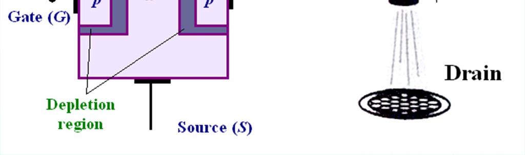
11 The basic construction of n-channel JFET is shown in the figure. The major part of the structure is the n- type of material, which forms the channel between the embedded layer of p-type material. The top of the n-type of material is connected to a terminal called drain (D), whereas the lower end called source (S).
12 The two p-type of material are connected together and to the gate (G) terminal. So the JFET has two p-n junctions under no-bias conditions. And a depletion region is generated at each junction with no free carrier. Also illustrated in the figure, it is the water analogy.
13 The water pressure can be likened to the applied voltage from drain to source (inside the JFET), which establishes a flow of water (electrons) from the spigot (source). For FET, the gate through an applied potential, controls the flow of current to the drain. The terminology, (D, G & S), is defined for electron flow.

14 Figure: JFET Construction
15 Biasing: V GS = 0, V DS > 0 As shown in the figure, a positive voltage V DS ( =V DD )is applied across the channel. The gate is connected directly to the source to establish the condition V GS = 0. The electrons are drawn to the drain, leading to the current I D, which is also the same as I S. And the I D is solely limited by the resistance of the n-channel between D & S.
16 The depletion region is wider near the top of both p-type materials. The reason is that upper region is more reverse-biased than the lower part, thus a wider depletion region. Also, the p-n junction is reverse-biased for the whole length of the channel, leading to no current in the gate terminal. I G = 0 is an important characteristic of JFET.
17 When V DS increasing, I D will also increase. As V DS increases, the depletion regions will widen, causing reduction in the channel width and a higher resistance. If V DS is increased to a level V P, where it appear that the two depletion regions would touch, a condition referred to as pinch-off will result.
18 The level of V DS that causes pinch-off condition is called pinch-off voltage, denoted by V P. Actually, under pinch-off condition, the current I D maintains a saturation level, defined as I DSS. I DSS is the maximum drain current for a JFET and is defined by the conditions V GS =0 and V DS > V P.

19 Figure: Biasing of JFET (V GS = 0, V DS > 0)
20 Figure: I D versus V DS for V GS = 0
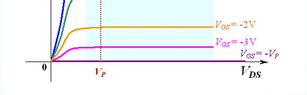
21 Biasing: V GS < 0 For BJT, the characteristics is plotted to show the relationship between I C and V CE for different levels of I B. For FET, the characteristics is drawn to show the relationship between I D and V DS for various levels of V GS. The V GS is the controlling voltage of JFET, just like I B for the BJT.
22 For the n-channel device, V GS is made more and more negative from its V GS = 0 level. The saturation level of I D has been reduced as V GS is made more and more negative. Eventually, when V GS = -V P, it is sufficiently negative to establish a saturation level that is zero.
23 For all practical purpose, the device has been turned off. The V GS that results in I D = 0 is defined by V GS = V P, with V P being a negative voltage for n-channel and a positive voltage for p- channel JFETs. The region to the right of the pinch-off locus is employed in linear amplifier and referred to as linear amplification region.

24 Figure: Biasing of JFET (V GS < 0)

25 Figure: JFET characteristics (V GS < 0)
26 Symbols of JFET The graphic symbols for the n-channel and p-channel JFETs are shown in the figure. Note that the arrow is pointing in for the n- channel device. This means that I G would flow if the p-n junction were forward-biased. For p-channel device, the only difference in the symbol is the direction of the arrow.
27 Figure: Symbols of JFET
28 Transfer Characteristics For BJT, the output current I C and input controlling current I B are related by constant, which is in the following equation form, I C = f(i B ) = I B For JFET, the relationship between the output and input quantities is not as simple as the that of BJT.
29 The relationship between the I D output and V GS is defined by Shockley s equation: I D I DSS V 1 GS VP where the I DSS and V P are constants, and V GS controls the I D. The squared term results in a nonlinear relationship between the I D output and V GS. 2
30 The transfer characteristics are properties of JFET itself and are unaffected by the network in which the device is used. Obviously, the transfer characteristics can be obtained by Shockley s equation. It can also be obtained from the output drain characteristics. We draw both curves with a common vertical scaling.
31 One is a plot of I D versus V DS, whereas the other is I D versus V GS. Using the drain characteristics on the right of the vertical axis, we can draw a horizontal line from the saturation region of the curve to the I D axis. The result current level for both graphs is I DSS.
32 The point of intersection on the I D versus V GS curve will be as shown since the vertical axis is defined as V GS = 0. If a horizontal line is drawn from the V GS = -1V curve to the I D axis and then extended to the other axis, another point on the transfer curve can be located. Continuing with V GS = -2V, -3V and V P (- 4V), we can complete the transfer curve.
33 The transfer characteristics are a plot of an output current I D versus an inputcontrolling quantity, V GS. It s a direct transfer from input to output variable. The non-linearity of the curve is obvious from the different space between curves of different V GS level, also from the curves themselves. It is the transfer curve of I D versus V GS that will receive extended use in the analysis of Chapter 7.
34 Shorthand Method The transfer curves are useful and there are ways to plot it. By Shockley s equation, it s precise but the calculation is time-consuming. By the drain characteristics, it s not easy since the drain characteristics should be known first. Here, a shorthand method will plot the curve in a efficient manner while maintaining an acceptable degree of accuracy.
35 The basic concept of the shorthand method is that the curve is sketched out with only several key points which are easy to obtain. First, from Shockley s equation V 1 GS I D I DSS VP If V GS = 0.5V P, then I D I DSS V / 2 1 P VP I DSS
36 If I D = 0.5I DSS, then 0 V.5 1 GS I DSS I DSS VP So we get V GS 0.3V P. If V GS = V P, then I D = 0. If V GS = 0, then I D = I DSS. So the transfer curve can be sketched to a satisfactory level of accuracy. 2
37 Figure: Transfer curve by shorthand method
38 p-channel JFET For p-channel devices, Shockley s equation can still be applied exactly as it appears. In this case, both V GS and V P will be positive. The transfer characteristics will be the mirror image of the transfer curve obtained with an n-channel and the same limiting values.
39 Figure: Transfer curve of p-channel JFET
40 Summary of JFET Important equations of JFET are as following: I D I V 1 GS VP I D = I S DSS I G 0 And the condition I G 0 is often the starting point for the analysis of a JFET configuration. 2
41 MOSFET: Depletion-Type The basic construction of n-channel depletiontype MOSFET is shown in the figure. A slab of p-type material forms substrate. The S & D are connected through metallic contacts to n-doped regions linked by an n- channel. The G is also connected to a metal contact, but insulated from the n-channel by a silicon dioxide (SiO 2 ) layer.
42 It is this layer of SiO 2 that accounts for I G = 0 and the desirable high input impedance of the device. Some devices provide an additional terminal labeled SS. But in most cases, the substrate and source are connected. From the above, the reason for the name of Metal Oxide Semiconductor FET is clear.


43 Figure: n-channel depletion-type MOSFET
44 Transfer Characteristics Shown in the figure, it is the configuration of n-channel depletion-type MOSFET. The substrate and source are connected as a three-terminal device. A positive potential is applied to V DS. An adjustable potential is applied to V GS. When V GS < 0, the transfer curve is like that of n-channel JFET.
45 When V GS > 0, the drain current I D will increase at a rapid rate. So the positive V GS has enhanced the level of I D and leads to the enhancement region. The region to the left of the vertical axis is the depletion region. The Shockley s equation is still be applicable for the depletion-type MOSFET.

46 Figure: Configuration of n-channel depletion-type MOSFET
47 For the plot of the transfer characteristics of an n-channel depletion-type MOSFET by shorthand method, please see Example 6.3. Shown in the figure, it s the transfer curve of the p-channel depletion-type MOSFET. It is exactly the opposite of that of n-channel. The V GS is positive for most of time and can also be negative. And when V GS = 0, I D = I DSS.
48 Symbols of Depletion-Type MOSFET The graphic symbols for the n-channel and p-channel depletion-type MOSFET are shown in the figure. The D & S is connected by channel through the vertical line in the symbol. The lack of a direct connection between G and channel is shown. The substrate is connected internally as a 3- terminal device.
49 Figure: Symbols of depletion-type MOSFET
50 MOSFET: Enhancement-Type Shown in the figure is the basic construction of n-channel enhancement-type MOSFET. A slab of p-type material forms substrate. The S & D are connected through metallic contacts to n-doped regions. The silicon dioxide (SiO 2 ) layer is still present to isolate the gate platform from the region between D & S.
51 Note the absence of a channel between the two n-doped regions. This is the primary difference between the construction of depletion-type and enhancement-type MOSFETs. The characteristics of the enhancementtype MOSFET are quite different from anything obtained thus far. The transfer curve is NOT defined by Shockley s equation.


52 Figure: n-channel enhancement-type MOSFET
53 Transfer Characteristics Shown in the figure, it is the configuration of n-channel enhancement-type MOSFET. The substrate and source are connected as a three-terminal device. A positive potential is applied to V DS. When V GS = 0, the absence of an n-channel will result in a zero current.
54 As V GS increases in magnitude, an induced n-type region is formed near the SiO 2 layer. This leads to a measurable current flow between D & S. The level of V GS that results in the significant increase in drain current I D is called the threshold voltage, V T. The channel is enhanced by V GS > 0. This is the reason to the name of this type of MOSFET.
55 If we hold V GS constant and increase V DS, the I D will eventually reach a saturation level. This is the result of the narrower channel at the drain end of the induced channel. The drain characteristics is shown in the figure. For a fixed value of V T, the higher level of V GS, the greater is the saturation level for V DS.
56 For V GS less than V T, I D = 0. It is noticeable that the spacing between the level of V GS increases as the magnitude of V GS increases. This shows the nonlinear relationship between I D and V GS. Actually, I D = k (V GS V T ) 2 where k is a constant and can be obtained through V GS(on) and I D(on) from datasheet.
57 Furthermore, transfer curve can be obtained by setting it side by side with drain characteristics. If a horizontal line is drawn from the V GS = +8V curve to the I D axis and then extended to the other axis, a point on the transfer curve can be located. Continuing with other voltages of V GS, the transfer curve is obtained.
58 It must be remembered that I D is zero for V GS V T. Also, the transfer curve is totally in the positive V GS region and does not rise until V GS = V T. As to how to plot the transfer curve given k and V T for a particular MOSFET, see Figure 6.37 on page 330.

59 Figure: Channel formation in the n-channel enhancement-type MOSFET
60 Figure: Drain & transfer characteristics for n-channel enhancement-type MOSFET
61 p-channel Enhancement-Type MOSFET The construction of p-channel enhancementtype MOSFET is exactly the reverse of that of n-channel one. A slab of n-type material forms substrate. Those p-doped regions are under the drain and source connections. All the voltage polarities and current directions are reversed.
62 The drain characteristics of p-channel enhancement-type MOSFET is shown in the figure. The I D is increasing from increasingly negative values of V GS. Also, I D is zero while V GS < V T. The equation of I D discussed before is also applicable to p-channel devices.
63 Symbols of Enhancement-Type MOSFET The graphic symbols for the n-channel and p-channel enhancement-type MOSFET are shown in the figure. The dashed line between D & S reflects that a channel does not exist. The direction of arrow shows the channel type of the device. The substrate is connected internally as a 3- terminal device.
64 Figure: Symbols of enhancement-type MOSFET
65 Summary of Chapter 6 Introduction to FET For JFET & MOSFET Output characteristics: I D ~V DS Transfer curves: I D ~V GS Shorthand method to sketch transfer curves Graphical symbols
FIELD EFFECT TRANSISTOR (FET) 1. JUNCTION FIELD EFFECT TRANSISTOR (JFET)
 1. JUNCTION FIELD EFFECT TRANSISTOR (JFET)") FIELD EFFECT TRANSISTOR (FET) The field-effect transistor (FET) is a three-terminal device used for a variety of applications that match, to a large extent, those of the BJT transistor. Although there
FIELD EFFECT TRANSISTOR (FET) The field-effect transistor (FET) is a three-terminal device used for a variety of applications that match, to a large extent, those of the BJT transistor. Although there
KOM2751 Analog Electronics :: Dr. Muharrem Mercimek :: YTU - Control and Automation Dept. 1 6 FIELD-EFFECT TRANSISTORS
 KOM2751 Analog Electronics :: Dr. Muharrem Mercimek :: YTU - Control and Automation Dept. 1 6 FIELD-EFFECT TRANSISTORS Most of the content is from the textbook: Electronic devices and circuit theory, Robert
FET(Field Effect Transistor)
") Field Effect Transistor: Construction and Characteristic of JFETs. Transfer Characteristic. CS,CD,CG amplifier and analysis of CS amplifier MOSFET (Depletion and Enhancement) Type, Transfer Characteristic,
Field Effect Transistor: Construction and Characteristic of JFETs. Transfer Characteristic. CS,CD,CG amplifier and analysis of CS amplifier MOSFET (Depletion and Enhancement) Type, Transfer Characteristic,
Field Effect Transistors
 Chapter 5: Field Effect Transistors Slide 1 FET FET s (Field Effect Transistors) are much like BJT s (Bipolar Junction Transistors). Similarities: Amplifiers Switching devices Impedance matching circuits
Chapter 6: Field-Effect Transistors
 Chapter 6: Field-Effect Transistors FETs vs. BJTs Similarities: Amplifiers Switching devices Impedance matching circuits Differences: FETs are voltage controlled devices. BJTs are current controlled devices.
Chapter 5: Field Effect Transistors
 Chapter 5: Field Effect Transistors Slide 1 FET FET s (Field Effect Transistors) are much like BJT s (Bipolar Junction Transistors). Similarities: Amplifiers Switching devices Impedance matching circuits
THE JFET. Script. Discuss the JFET and how it differs from the BJT. Describe the basic structure of n-channel and p -channel JFETs
 Course: B.Sc. Applied Physical Science (Computer Science) Year & Sem.: Ist Year, Sem - IInd Subject: Electronics Paper No.: V Paper Title: Analog Circuits Lecture No.: 12 Lecture Title: Analog Circuits
FET. FET (field-effect transistor) JFET. Prepared by Engr. JP Timola Reference: Electronic Devices by Floyd
 JFET. Prepared by Engr. JP Timola Reference: Electronic Devices by Floyd") FET Prepared by Engr. JP Timola Reference: Electronic Devices by Floyd FET (field-effect transistor) unipolar devices - unlike BJTs that use both electron and hole current, they operate only with one type
FET Prepared by Engr. JP Timola Reference: Electronic Devices by Floyd FET (field-effect transistor) unipolar devices - unlike BJTs that use both electron and hole current, they operate only with one type
Basic Electronics Prof. Dr. Chitralekha Mahanta Department of Electronics and Communication Engineering Indian Institute of Technology, Guwahati
 Basic Electronics Prof. Dr. Chitralekha Mahanta Department of Electronics and Communication Engineering Indian Institute of Technology, Guwahati Module: 3 Field Effect Transistors Lecture-7 High Frequency
CHAPTER 8 FIELD EFFECT TRANSISTOR (FETs)
") CHAPTER 8 FIELD EFFECT TRANSISTOR (FETs) INTRODUCTION - FETs are voltage controlled devices as opposed to BJT which are current controlled. - There are two types of FETs. o Junction FET (JFET) o Metal
CHAPTER 8 FIELD EFFECT TRANSISTOR (FETs) INTRODUCTION - FETs are voltage controlled devices as opposed to BJT which are current controlled. - There are two types of FETs. o Junction FET (JFET) o Metal
Lecture 15. Field Effect Transistor (FET) Wednesday 29/11/2017 MOSFET 1-1
 Wednesday 29/11/2017 MOSFET 1-1") Lecture 15 Field Effect Transistor (FET) Wednesday 29/11/2017 MOSFET 1-1 Outline MOSFET transistors Introduction to MOSFET MOSFET Types epletion-type MOSFET Characteristics Comparison between JFET and
Lecture 15 Field Effect Transistor (FET) Wednesday 29/11/2017 MOSFET 1-1 Outline MOSFET transistors Introduction to MOSFET MOSFET Types epletion-type MOSFET Characteristics Comparison between JFET and
(a) Current-controlled and (b) voltage-controlled amplifiers.
 Current-controlled and (b) voltage-controlled amplifiers.") Fig. 6.1 (a) Current-controlled and (b) voltage-controlled amplifiers. Fig. 6.2 Drs. Ian Munro Ross (front) and G. C. Dacey jointly developed an experimental procedure for measuring the characteristics
Fig. 6.1 (a) Current-controlled and (b) voltage-controlled amplifiers. Fig. 6.2 Drs. Ian Munro Ross (front) and G. C. Dacey jointly developed an experimental procedure for measuring the characteristics
MODULE-2: Field Effect Transistors (FET)
") FORMAT-1B Definition: MODULE-2: Field Effect Transistors (FET) FET is a three terminal electronic device used for variety of applications that match with BJT. In FET, an electric field is established by
FORMAT-1B Definition: MODULE-2: Field Effect Transistors (FET) FET is a three terminal electronic device used for variety of applications that match with BJT. In FET, an electric field is established by
Lecture 13. Metal Oxide Semiconductor Field Effect Transistor (MOSFET) MOSFET 1-1
 MOSFET 1-1") Lecture 13 Metal Oxide Semiconductor Field Effect Transistor (MOSFET) MOSFET 1-1 Outline Continue MOSFET Qualitative Operation epletion-type MOSFET Characteristics Biasing Circuits and Examples Enhancement-type
Lecture 13 Metal Oxide Semiconductor Field Effect Transistor (MOSFET) MOSFET 1-1 Outline Continue MOSFET Qualitative Operation epletion-type MOSFET Characteristics Biasing Circuits and Examples Enhancement-type
FET. Field Effect Transistors ELEKTRONIKA KONTROL. Eka Maulana, ST, MT, M.Eng. Universitas Brawijaya. p + S n n-channel. Gate. Basic structure.
 FET Field Effect Transistors ELEKTRONIKA KONTROL Basic structure Gate G Source S n n-channel Cross section p + p + p + G Depletion region Drain D Eka Maulana, ST, MT, M.Eng. Universitas Brawijaya S Channel
Field Effect Transistor (FET) FET 1-1
 FET 1-1") Field Effect Transistor (FET) FET 1-1 Outline MOSFET transistors ntroduction to MOSFET MOSFET Types epletion-type MOSFET Characteristics Biasing Circuits and Examples Comparison between JFET and epletion-type
Field Effect Transistor (FET) FET 1-1 Outline MOSFET transistors ntroduction to MOSFET MOSFET Types epletion-type MOSFET Characteristics Biasing Circuits and Examples Comparison between JFET and epletion-type
IENGINEERS-CONSULTANTS QUESTION BANK SERIES ELECTRONICS ENGINEERING 1 YEAR UPTU ELECTRONICS ENGINEERING EC 101 UNIT 3 (JFET AND MOSFET)
") ELECTRONICS ENGINEERING EC 101 UNIT 3 (JFET AND MOSFET) LONG QUESTIONS (10 MARKS) 1. Draw the construction diagram and explain the working of P-Channel JFET. Also draw the characteristics curve and transfer
ELECTRONICS ENGINEERING EC 101 UNIT 3 (JFET AND MOSFET) LONG QUESTIONS (10 MARKS) 1. Draw the construction diagram and explain the working of P-Channel JFET. Also draw the characteristics curve and transfer
Chapter 6: Field-Effect Transistors
 Chapter 6: Field-Effect Transistors Islamic University of Gaza Dr. Talal Skaik MOSFETs MOSFETs have characteristics similar to JFETs and additional characteristics that make then very useful. There are
Lecture 14. Field Effect Transistor (FET) Sunday 26/11/2017 FET 1-1
 Sunday 26/11/2017 FET 1-1") Lecture 14 Field Effect Transistor (FET) Sunday 26/11/2017 FET 1-1 Outline Introduction to FET transistors Types of FET Transistors Junction Field Effect Transistor (JFET) Characteristics Construction
Lecture 14 Field Effect Transistor (FET) Sunday 26/11/2017 FET 1-1 Outline Introduction to FET transistors Types of FET Transistors Junction Field Effect Transistor (JFET) Characteristics Construction
KOREA UNIVERSITY. Photonics Laboratory. Ch 15. Field effect Introduction-The J-FET and MESFET
 Ch 15. Field effect Introduction-The J-FET and MESFET : (a) The device worked on the principle that a voltage applied to the metallic plate modulated the conductance of the underlying semiconductor, which
Lecture 17. Field Effect Transistor (FET) FET 1-1
 FET 1-1") Lecture 17 Field Effect Transistor (FET) FET 1-1 Outline ntroduction to FET transistors Comparison with BJT transistors FET Types Construction and Operation of FET Characteristics Of FET Examples FET 1-2
Lecture 17 Field Effect Transistor (FET) FET 1-1 Outline ntroduction to FET transistors Comparison with BJT transistors FET Types Construction and Operation of FET Characteristics Of FET Examples FET 1-2
UNIT 3: FIELD EFFECT TRANSISTORS
 FIELD EFFECT TRANSISTOR: UNIT 3: FIELD EFFECT TRANSISTORS The field effect transistor is a semiconductor device, which depends for its operation on the control of current by an electric field. There are
Analog Electronics. Electronic Devices, 9th edition Thomas L. Floyd Pearson Education. Upper Saddle River, NJ, All rights reserved.
 Analog Electronics BJT Structure The BJT has three regions called the emitter, base, and collector. Between the regions are junctions as indicated. The base is a thin lightly doped region compared to the
(Refer Slide Time: 02:05)
") Electronics for Analog Signal Processing - I Prof. K. Radhakrishna Rao Department of Electrical Engineering Indian Institute of Technology Madras Lecture 27 Construction of a MOSFET (Refer Slide Time:
Electronics for Analog Signal Processing - I Prof. K. Radhakrishna Rao Department of Electrical Engineering Indian Institute of Technology Madras Lecture 27 Construction of a MOSFET (Refer Slide Time:
Field-Effect Transistor
 Philadelphia University Faculty of Engineering Communication and Electronics Engineering Field-Effect Transistor Introduction FETs (Field-Effect Transistors) are much like BJTs (Bipolar Junction Transistors).
Digital Electronics. By: FARHAD FARADJI, Ph.D. Assistant Professor, Electrical and Computer Engineering, K. N. Toosi University of Technology
 K. N. Toosi University of Technology Chapter 7. Field-Effect Transistors By: FARHAD FARADJI, Ph.D. Assistant Professor, Electrical and Computer Engineering, K. N. Toosi University of Technology http://wp.kntu.ac.ir/faradji/digitalelectronics.htm
Three Terminal Devices
 Three Terminal Devices - field effect transistor (FET) - bipolar junction transistor (BJT) - foundation on which modern electronics is built - active devices - devices described completely by considering
EDC UNIT IV- Transistor and FET Characteristics EDC Lesson 9- ", Raj Kamal, 1
 EDC UNIT IV- Transistor and FET Characteristics Lesson-9: JFET and Construction of JFET 2008 EDC Lesson 9- ", Raj Kamal, 1 1. Transistor 2008 EDC Lesson 9- ", Raj Kamal, 2 Transistor Definition The transferred-resistance
ITT Technical Institute. ET215 Devices 1. Unit 8 Chapter 4, Sections
 ITT Technical Institute ET215 Devices 1 Unit 8 Chapter 4, Sections 4.4 4.5 Chapter 4 Section 4.4 MOSFET Characteristics A Metal-Oxide semiconductor field-effect transistor is the other major category of
Lecture 20. MOSFET (cont d) MOSFET 1-1
 MOSFET 1-1") Lecture 0 MOSFET (cont d) MOSFET 1-1 Outline Continue Enhancement-type MOSFET (E- MOSFET) Characteristics C Biasing Circuits and Examples MOSFET 1- Test Yourself Complete the following statements with
Lecture 0 MOSFET (cont d) MOSFET 1-1 Outline Continue Enhancement-type MOSFET (E- MOSFET) Characteristics C Biasing Circuits and Examples MOSFET 1- Test Yourself Complete the following statements with
EIE209 Basic Electronics. Transistor Devices. Contents BJT and FET Characteristics Operations. Prof. C.K. Tse: T ransistor devices
 EIE209 Basic Electronics Transistor Devices Contents BJT and FET Characteristics Operations 1 What is a transistor? Three-terminal device whose voltage-current relationship is controlled by a third voltage
Electronic Circuits. Junction Field-effect Transistors. Dr. Manar Mohaisen Office: F208 Department of EECE
 Electronic Circuits Junction Field-effect Transistors Dr. Manar Mohaisen Office: F208 Email: manar.subhi@kut.ac.kr Department of EECE Review of the Precedent Lecture Explain the Operation Class A Power
Chapter 8. Field Effect Transistor
 Chapter 8. Field Effect Transistor Field Effect Transistor: The field effect transistor is a semiconductor device, which depends for its operation on the control of current by an electric field. There
Summary. Electronics II Lecture 5(b): Metal-Oxide Si FET MOSFET. A/Lectr. Khalid Shakir Dept. Of Electrical Engineering
: Metal-Oxide Si FET MOSFET. A/Lectr. Khalid Shakir Dept. Of Electrical Engineering") Summary Electronics II Lecture 5(b): Metal-Oxide Si FET MOSFET A/Lectr. Khalid Shakir Dept. Of Electrical Engineering College of Engineering Maysan University Page 1-21 Summary The MOSFET The metal oxide
Summary Electronics II Lecture 5(b): Metal-Oxide Si FET MOSFET A/Lectr. Khalid Shakir Dept. Of Electrical Engineering College of Engineering Maysan University Page 1-21 Summary The MOSFET The metal oxide
Depletion-mode operation ( 공핍형 ): Using an input gate voltage to effectively decrease the channel size of an FET
: Using an input gate voltage to effectively decrease the channel size of an FET") Ch. 13 MOSFET Metal-Oxide-Semiconductor Field-Effect Transistor : I D D-mode E-mode V g The gate oxide is made of dielectric SiO 2 with e = 3.9 Depletion-mode operation ( 공핍형 ): Using an input gate voltage
Ch. 13 MOSFET Metal-Oxide-Semiconductor Field-Effect Transistor : I D D-mode E-mode V g The gate oxide is made of dielectric SiO 2 with e = 3.9 Depletion-mode operation ( 공핍형 ): Using an input gate voltage
L MOSFETS, IDENTIFICATION, CURVES. PAGE 1. I. Review of JFET (DRAW symbol for n-channel type, with grounded source)
") L.107.4 MOSFETS, IDENTIFICATION, CURVES. PAGE 1 I. Review of JFET (DRAW symbol for n-channel type, with grounded source) 1. "normally on" device A. current from source to drain when V G = 0 no need to
L.107.4 MOSFETS, IDENTIFICATION, CURVES. PAGE 1 I. Review of JFET (DRAW symbol for n-channel type, with grounded source) 1. "normally on" device A. current from source to drain when V G = 0 no need to
UNIT I - TRANSISTOR BIAS STABILITY
 UNIT I - TRANSISTOR BIAS STABILITY OBJECTIVE On the completion of this unit the student will understand NEED OF BIASING CONCEPTS OF LOAD LINE Q-POINT AND ITS STABILIZATION AND COMPENSATION DIFFERENT TYPES
Field-Effect Transistor
 Module: Electronics Module Number: 610/6501- Philadelphia University Faculty of Engineering Communication and Electronics Engineering Field-Effect Transistor ntroduction FETs (Field-Effect Transistors)
I E I C since I B is very small
 Figure 2: Symbols and nomenclature of a (a) npn and (b) pnp transistor. The BJT consists of three regions, emitter, base, and collector. The emitter and collector are usually of one type of doping, while
Q1. Explain the construction and principle of operation of N-Channel and P-Channel Junction Field Effect Transistor (JFET).
.") Q. Explain the construction and principle of operation of N-Channel and P-Channel Junction Field Effect Transistor (JFET). Answer: N-Channel Junction Field Effect Transistor (JFET) Construction: Drain(D)
Q. Explain the construction and principle of operation of N-Channel and P-Channel Junction Field Effect Transistor (JFET). Answer: N-Channel Junction Field Effect Transistor (JFET) Construction: Drain(D)
KOM2751 Analog Electronics :: Dr. Muharrem Mercimek :: YTU - Control and Automation Dept. 1 7 DC BIASING FETS
 KOM751 Analog Electronics :: Dr. Muharrem Mercimek :: YTU Control and Automation Dept. 1 7 DC BIASING FETS Most of the content is from the textbook: Electronic devices and circuit theory, Robert L. Boylestad,
Electronics I. Last Time
 (Rev. 1.0) Electronics I Lecture 28 Introduction to Field Effect Transistors (FET s) Muhammad Tilal Department of Electrical Engineering CIIT Attock Campus The logo and is the property of CIIT, Pakistan
Field-Effect Transistor (FET) is one of the two major transistors; FET derives its name from its working mechanism;
 is one of the two major transistors; FET derives its name from its working mechanism;") Chapter 3 Field-Effect Transistors (FETs) 3.1 Introduction Field-Effect Transistor (FET) is one of the two major transistors; FET derives its name from its working mechanism; The concept has been known
Chapter 3 Field-Effect Transistors (FETs) 3.1 Introduction Field-Effect Transistor (FET) is one of the two major transistors; FET derives its name from its working mechanism; The concept has been known
FIELD EFFECT TRANSISTORS MADE BY : GROUP (13)/PM
/PM") FIELD EFFECT TRANSISTORS MADE BY : GROUP (13)/PM THE FIELD EFFECT TRANSISTOR (FET) In 1945, Shockley had an idea for making a solid state device out of semiconductors. He reasoned that a strong electrical
FIELD EFFECT TRANSISTORS MADE BY : GROUP (13)/PM THE FIELD EFFECT TRANSISTOR (FET) In 1945, Shockley had an idea for making a solid state device out of semiconductors. He reasoned that a strong electrical
UNIT-VI FIELD EFFECT TRANSISTOR. 1. Explain about the Field Effect Transistor and also mention types of FET s.
 UNIT-I FIELD EFFECT TRANSISTOR 1. Explain about the Field Effect Transistor and also mention types of FET s. The Field Effect Transistor, or simply FET however, uses the voltage that is applied to their
Unit III FET and its Applications. 2 Marks Questions and Answers
 Unit III FET and its Applications 2 Marks Questions and Answers 1. Why do you call FET as field effect transistor? The name field effect is derived from the fact that the current is controlled by an electric
EE70 - Intro. Electronics
 EE70 - Intro. Electronics Course website: ~/classes/ee70/fall05 Today s class agenda (November 28, 2005) review Serial/parallel resonant circuits Diode Field Effect Transistor (FET) f 0 = Qs = Qs = 1 2π
PESIT Bangalore South Campus
 INTERNAL ASSESSMENT TEST 2 Date : 19/09/2016 Max Marks: 40 Subject & Code : Analog and Digital Electronics (15CS32) Section: III A and B Name of faculty: Deepti.C Time : 8:30 am-10:00 am Note: Answer five
INTRODUCTION: Basic operating principle of a MOSFET:
 INTRODUCTION: Along with the Junction Field Effect Transistor (JFET), there is another type of Field Effect Transistor available whose Gate input is electrically insulated from the main current carrying
MEASUREMENT AND INSTRUMENTATION STUDY NOTES UNIT-I
 MEASUREMENT AND INSTRUMENTATION STUDY NOTES The MOSFET The MOSFET Metal Oxide FET UNIT-I As well as the Junction Field Effect Transistor (JFET), there is another type of Field Effect Transistor available
Field Effect Transistors (npn)
") Field Effect Transistors (npn) gate drain source FET 3 terminal device channel e - current from source to drain controlled by the electric field generated by the gate base collector emitter BJT 3 terminal
Field Effect Transistors (npn) gate drain source FET 3 terminal device channel e - current from source to drain controlled by the electric field generated by the gate base collector emitter BJT 3 terminal
Physics 364, Fall 2012, reading due your answers to by 11pm on Thursday
 Physics 364, Fall 2012, reading due 2012-10-25. Email your answers to ashmansk@hep.upenn.edu by 11pm on Thursday Course materials and schedule are at http://positron.hep.upenn.edu/p364 Assignment: (a)
UNIT-1 Bipolar Junction Transistors. Text Book:, Microelectronic Circuits 6 ed., by Sedra and Smith, Oxford Press
 UNIT-1 Bipolar Junction Transistors Text Book:, Microelectronic Circuits 6 ed., by Sedra and Smith, Oxford Press Figure 6.1 A simplified structure of the npn transistor. Microelectronic Circuits, Sixth
Lecture 18. MOSFET (cont d) MOSFET 1-1
 MOSFET 1-1") Lecture 18 MOSFET (cont d) MOSFET 1-1 Outline Continue Enhancement-type MOSFET (E- MOSFET) Characteristics C Biasing Circuits and Examples MOSFET 1- E-MOSFET (Quick Review) MOSFET is also known as nsulated-gate
Lecture 18 MOSFET (cont d) MOSFET 1-1 Outline Continue Enhancement-type MOSFET (E- MOSFET) Characteristics C Biasing Circuits and Examples MOSFET 1- E-MOSFET (Quick Review) MOSFET is also known as nsulated-gate
ITT Technical Institute. ET215 Devices 1. Unit 7 Chapter 4, Sections
 ITT Technical Institute ET215 Devices 1 Unit 7 Chapter 4, Sections 4.1 4.3 Chapter 4 Section 4.1 Structure of Field-Effect Transistors Recall that the BJT is a current-controlling device; the field-effect
4.2.2 Metal Oxide Semiconductor Field Effect Transistor (MOSFET)
") 4.2.2 Metal Oxide Semiconductor Field Effect Transistor (MOSFET) The Metal Oxide Semitonductor Field Effect Transistor (MOSFET) has two modes of operation, the depletion mode, and the enhancement mode.
4.2.2 Metal Oxide Semiconductor Field Effect Transistor (MOSFET) The Metal Oxide Semitonductor Field Effect Transistor (MOSFET) has two modes of operation, the depletion mode, and the enhancement mode.
FIELD EFFECT TRANSISTORS
 FIELD EFFECT TRANSISTORS Module 5 Introduction Symbol Features: 1. Voltage is applied across gate and source terminals. This voltage controls the drain current. Hence FET is a voltage controlled device.
Field - Effect Transistor
 Page 1 of 6 Field - Effect Transistor Aim :- To draw and study the out put and transfer characteristics of the given FET and to determine its parameters. Apparatus :- FET, two variable power supplies,
Chapter Two "Bipolar Transistor Circuits"
 Chapter Two "Bipolar Transistor Circuits" 1.TRANSISTOR CONSTRUCTION:- The transistor is a three-layer semiconductor device consisting of either two n- and one p-type layers of material or two p- and one
TRANSISTOR TRANSISTOR
 It is made up of semiconductor material such as Si and Ge. Usually, it comprises of three terminals namely, base, emitter and collector for providing connection to the external circuit. Today, some transistors
Prof. Paolo Colantonio a.a
 Prof. Paolo Colantonio a.a. 20 2 Field effect transistors (FETs) are probably the simplest form of transistor, widely used in both analogue and digital applications They are characterised by a very high
Lecture (10) MOSFET. By: Dr. Ahmed ElShafee. Dr. Ahmed ElShafee, ACU : Fall 2016, Electronic Circuits II
 MOSFET. By: Dr. Ahmed ElShafee. Dr. Ahmed ElShafee, ACU : Fall 2016, Electronic Circuits II") Lecture (10) MOSFET By: Dr. Ahmed ElShafee ١ Dr. Ahmed ElShafee, ACU : Fall 2017, Electronic Circuits II Introduction The MOSFET (metal oxide semiconductor field effect transistor) is another category
Lecture (10) MOSFET By: Dr. Ahmed ElShafee ١ Dr. Ahmed ElShafee, ACU : Fall 2017, Electronic Circuits II Introduction The MOSFET (metal oxide semiconductor field effect transistor) is another category
Transistor Characteristics
 Transistor Characteristics Introduction Transistors are the most recent additions to a family of electronic current flow control devices. They differ from diodes in that the level of current that can flow
Basic Electronics Prof. Dr. Chitralekha Mahanta Department of Electronics and Communication Engineering Indian Institute of Technology, Guwahati
 Basic Electronics Prof. Dr. Chitralekha Mahanta Department of Electronics and Communication Engineering Indian Institute of Technology, Guwahati Module: 3 Field Effect Transistors Lecture-8 Junction Field
Semiconductor Physics and Devices
 Metal-Semiconductor and Semiconductor Heterojunctions The Metal-Oxide-Semiconductor Field-Effect Transistor (MOSFET) is one of two major types of transistors. The MOSFET is used in digital circuit, because
Lesson 5. Electronics: Semiconductors Doping p-n Junction Diode Half Wave and Full Wave Rectification Introduction to Transistors-
 Lesson 5 Electronics: Semiconductors Doping p-n Junction Diode Half Wave and Full Wave Rectification Introduction to Transistors- Types and Connections Semiconductors Semiconductors If there are many free
EE301 Electronics I , Fall
 EE301 Electronics I 2018-2019, Fall 1. Introduction to Microelectronics (1 Week/3 Hrs.) Introduction, Historical Background, Basic Consepts 2. Rewiev of Semiconductors (1 Week/3 Hrs.) Semiconductor materials
Lecture - 18 Transistors
 Electronic Materials, Devices and Fabrication Dr. S. Prarasuraman Department of Metallurgical and Materials Engineering Indian Institute of Technology, Madras Lecture - 18 Transistors Last couple of classes
UNIT 3 Transistors JFET
 UNIT 3 Transistors JFET Mosfet Definition of BJT A bipolar junction transistor is a three terminal semiconductor device consisting of two p-n junctions which is able to amplify or magnify a signal. It
UNIT 4 BIASING AND STABILIZATION
 UNIT 4 BIASING AND STABILIZATION TRANSISTOR BIASING: To operate the transistor in the desired region, we have to apply external dec voltages of correct polarity and magnitude to the two junctions of the
Conduction Characteristics of MOS Transistors (for fixed Vds)! Topic 2. Basic MOS theory & SPICE simulation. MOS Transistor
! Topic 2. Basic MOS theory & SPICE simulation. MOS Transistor") Conduction Characteristics of MOS Transistors (for fixed Vds)! Topic 2 Basic MOS theory & SPICE simulation Peter Cheung Department of Electrical & Electronic Engineering Imperial College London (Weste&Harris,
Conduction Characteristics of MOS Transistors (for fixed Vds)! Topic 2 Basic MOS theory & SPICE simulation Peter Cheung Department of Electrical & Electronic Engineering Imperial College London (Weste&Harris,
Topic 2. Basic MOS theory & SPICE simulation
 Topic 2 Basic MOS theory & SPICE simulation Peter Cheung Department of Electrical & Electronic Engineering Imperial College London (Weste&Harris, Ch 2 & 5.1-5.3 Rabaey, Ch 3) URL: www.ee.ic.ac.uk/pcheung/
Conduction Characteristics of MOS Transistors (for fixed Vds) Topic 2. Basic MOS theory & SPICE simulation. MOS Transistor
 Topic 2. Basic MOS theory & SPICE simulation. MOS Transistor") Conduction Characteristics of MOS Transistors (for fixed Vds) Topic 2 Basic MOS theory & SPICE simulation Peter Cheung Department of Electrical & Electronic Engineering Imperial College London (Weste&Harris,
Conduction Characteristics of MOS Transistors (for fixed Vds) Topic 2 Basic MOS theory & SPICE simulation Peter Cheung Department of Electrical & Electronic Engineering Imperial College London (Weste&Harris,
EE 5611 Introduction to Microelectronic Technologies Fall Thursday, September 04, 2014 Lecture 02
 EE 5611 Introduction to Microelectronic Technologies Fall 2014 Thursday, September 04, 2014 Lecture 02 1 Lecture Outline Review on semiconductor materials Review on microelectronic devices Example of microelectronic
Design cycle for MEMS
 Design cycle for MEMS Design cycle for ICs IC Process Selection nmos CMOS BiCMOS ECL for logic for I/O and driver circuit for critical high speed parts of the system The Real Estate of a Wafer MOS Transistor
Laboratory #5 BJT Basics and MOSFET Basics
 Laboratory #5 BJT Basics and MOSFET Basics I. Objectives 1. Understand the physical structure of BJTs and MOSFETs. 2. Learn to measure I-V characteristics of BJTs and MOSFETs. II. Components and Instruments
5.1 Introduction. transistor. Like the bipolar junction transistors (BJTs) we studied in Chapter 4,
 we studied in Chapter 4,") 5.1 Introduction In this chapter we introduce the second major type of transistor: the field-effect transistor. Like the bipolar junction transistors (BJTs) we studied in Chapter 4, field-effect transistors
5.1 Introduction In this chapter we introduce the second major type of transistor: the field-effect transistor. Like the bipolar junction transistors (BJTs) we studied in Chapter 4, field-effect transistors
Field Effect Transistors
 Field Effect Transistors LECTURE NO. - 41 Field Effect Transistors www.mycsvtunotes.in JFET MOSFET CMOS Field Effect transistors - FETs First, why are we using still another transistor? BJTs had a small
Difference between BJTs and FETs. Junction Field Effect Transistors (JFET)
") Difference between BJTs and FETs Transistors can be categorized according to their structure, and two of the more commonly known transistor structures, are the BJT and FET. The comparison between BJTs
Difference between BJTs and FETs Transistors can be categorized according to their structure, and two of the more commonly known transistor structures, are the BJT and FET. The comparison between BJTs
Radio Frequency Electronics
 Radio Frequency Electronics Active Components II Harry Nyquist Born in 1889 in Sweden Received B.S. and M.S. from U. North Dakota Received Ph.D. from Yale Worked and Bell Laboratories for all of his career
Field Effect Transistors
 Field Effect Transistors Purpose In this experiment we introduce field effect transistors (FETs). We will measure the output characteristics of a FET, and then construct a common-source amplifier stage,
FIELD- EFFECT TRANSISTORS: MOSFETS
 FIELD- EFFECT TRANSISTORS: MOSFETS LAB 8: INTRODUCTION TO FETS AND USING THEM AS CURRENT CONTROLLERS As discussed in the last lab, transistors are the basic devices providing control of large currents
AE103 ELECTRONIC DEVICES & CIRCUITS DEC 2014
 Q.2 a. State and explain the Reciprocity Theorem and Thevenins Theorem. a. Reciprocity Theorem: If we consider two loops A and B of network N and if an ideal voltage source E in loop A produces current
Figure 1: JFET common-source amplifier. A v = V ds V gs
 Chapter 7: FET Amplifiers Switching and Circuits The Common-Source Amplifier In a common-source (CS) amplifier, the input signal is applied to the gate and the output signal is taken from the drain. The
The Common Source JFET Amplifier
 The Common Source JFET Amplifier Small signal amplifiers can also be made using Field Effect Transistors or FET's for short. These devices have the advantage over bipolar transistors of having an extremely
BJT. Bipolar Junction Transistor BJT BJT 11/6/2018. Dr. Satish Chandra, Assistant Professor, P P N College, Kanpur 1
 BJT Bipolar Junction Transistor Satish Chandra Assistant Professor Department of Physics P P N College, Kanpur www.satish0402.weebly.com The Bipolar Junction Transistor is a semiconductor device which
An introduction to Depletion-mode MOSFETs By Linden Harrison
 An introduction to Depletion-mode MOSFETs By Linden Harrison Since the mid-nineteen seventies the enhancement-mode MOSFET has been the subject of almost continuous global research, development, and refinement
Frequently Asked Questions
 Course: B.Sc. Applied Physical Science (Computer Science) Year & Sem.: Ist Year, Sem - IInd Subject: Electronics Paper No.: V Paper Title: Analog Circuits Lecture No.: 13 Lecture Title: Analog Circuits
In this lecture we will begin a new topic namely the Metal-Oxide-Semiconductor Field Effect Transistor.
 Solid State Devices Dr. S. Karmalkar Department of Electronics and Communication Engineering Indian Institute of Technology, Madras Lecture - 38 MOS Field Effect Transistor In this lecture we will begin
Lecture 3: Transistors
 Lecture 3: Transistors Now that we know about diodes, let s put two of them together, as follows: collector base emitter n p n moderately doped lightly doped, and very thin heavily doped At first glance,
Gechstudentszone.wordpress.com
 UNIT 4: Small Signal Analysis of Amplifiers 4.1 Basic FET Amplifiers In the last chapter, we described the operation of the FET, in particular the MOSFET, and analyzed and designed the dc response of circuits
F.Y. Diploma : Sem. II [DE/EJ/IE/IS/EE/MU/ET/EN/EX] Basic Electronics
![F.Y. Diploma : Sem. II [DE/EJ/IE/IS/EE/MU/ET/EN/EX] Basic Electronics](/thumbs/95/124107511.jpg "F.Y. Diploma : Sem. II [DE/EJ/IE/IS/EE/MU/ET/EN/EX] Basic Electronics") F.Y. Diploma : Sem. II [DE/EJ/IE/IS/EE/MU/ET/EN/EX] Basic Electronics Time: 3 Hrs.] Prelim Question Paper Solution [Marks : 70 Q.1 Attempt any FIE of the following : [10] Q.1(a) Draw the symbols for (i)
F.Y. Diploma : Sem. II [DE/EJ/IE/IS/EE/MU/ET/EN/EX] Basic Electronics Time: 3 Hrs.] Prelim Question Paper Solution [Marks : 70 Q.1 Attempt any FIE of the following : [10] Q.1(a) Draw the symbols for (i)
Lecture (09) The JFET (2)
 The JFET (2)") Lecture (09) The JFET (2) By: r. Ahmed Elhafee ١ V Controls I connect a bias voltage, V V is set to increasingly more negative values by adjusting V, a family of drain characteristic curves is produced.
Lecture (09) The JFET (2) By: r. Ahmed Elhafee ١ V Controls I connect a bias voltage, V V is set to increasingly more negative values by adjusting V, a family of drain characteristic curves is produced.
Student Lecture by: Giangiacomo Groppi Joel Cassell Pierre Berthelot September 28 th 2004
 Student Lecture by: Giangiacomo Groppi Joel Cassell Pierre Berthelot September 28 th 2004 Lecture outline Historical introduction Semiconductor devices overview Bipolar Junction Transistor (BJT) Field
INTRODUCTION TO MOS TECHNOLOGY
 INTRODUCTION TO MOS TECHNOLOGY 1. The MOS transistor The most basic element in the design of a large scale integrated circuit is the transistor. For the processes we will discuss, the type of transistor
Lecture 16. MOSFET (cont d) Sunday 3/12/2017 MOSFET 1-1
 Sunday 3/12/2017 MOSFET 1-1") Lecture 16 MOSFET (cont d) Sunday 3/1/017 MOSFET 1-1 Outline Continue Enhancement-type MOSFET Characteristics C Biasing Circuits and Examples ntroduction to BJT-FET Combination Circuits Combination of
Lecture 16 MOSFET (cont d) Sunday 3/1/017 MOSFET 1-1 Outline Continue Enhancement-type MOSFET Characteristics C Biasing Circuits and Examples ntroduction to BJT-FET Combination Circuits Combination of
Chapter 8: Field Effect Transistors
 Chapter 8: Field Effect Transistors Transistors are different from the basic electronic elements in that they have three terminals. Consequently, we need more parameters to describe their behavior than
Chapter 3 Bipolar Junction Transistors (BJT)
") Chapter 3 Bipolar Junction Transistors (BJT) Transistors In analog circuits, transistors are used in amplifiers and linear regulated power supplies. In digital circuits they function as electrical switches,
Chapter 3 Bipolar Junction Transistors (BJT) Transistors In analog circuits, transistors are used in amplifiers and linear regulated power supplies. In digital circuits they function as electrical switches,
Electronic Circuits II - Revision
 Electronic Circuits II - Revision -1 / 16 - T & F # 1 A bypass capacitor in a CE amplifier decreases the voltage gain. 2 If RC in a CE amplifier is increased, the voltage gain is reduced. 3 4 5 The load
4.1 Device Structure and Physical Operation
 10/12/2004 4_1 Device Structure and Physical Operation blank.doc 1/2 4.1 Device Structure and Physical Operation Reading Assignment: pp. 235-248 Chapter 4 covers Field Effect Transistors ( ) Specifically,