Power semiconductors. José M. Cámara V 1.0
|
|
|
- Winfred Patrick
- 5 years ago
- Views:
Transcription


1 Power semiconductors José M. Cámara V 1.0
2 Introduction Here we are going to study semiconductor devices used in power electronics. They work under medium and high currents and voltages. Some of them only exist as power devices. Other are equivalent to their signal counterparts but handling higher currents and voltages. Unlike signal devices they usually work in switch mode. The following ones will be considered: Diodes Transistors Thyristors Other devices
3 Power diodes - Introduction They have signal counterparts. Like them, they are made from a single p-n junction. Chip area and conducted current are higher. They have to achieve the following requirements: When forward biased, they have to conduct high currents with low voltage drop. When reverse biased, they have to withstand a high reverse voltage with low leakage current. They must get back to the blocking state after conduction swiftly and with a low reverse current.
4 Power diodes - Blocking It happens when the cathode is made more positive than the anode. This results in: Migration of the majority charge carriers to the area near the terminals. The depletion region widens. Appearance of a voltage barrier at the junction approximately as high as the applied voltage. Minority charge carriers current dependent on the temperature, not the voltage. Associated parameters: Maximum DC reverse voltage: the maximum amount of voltage the diode can withstand in reverse-bias mode on a continual basis. Maximum reverse repetitive voltage: the maximum amount of voltage the diode can withstand in reverse-bias mode, in repeated pulses of 1ms every 10ms. Peak reverse voltage: maximum reverse bias voltage can be applied to diode which does not cause break down. The diode can withstand it for 10 ms every 10. Breakdown voltage: can destroy the diode.
5 Power diodes - Conduction It happens when the anode is made more positive than the cathode. This results in: Migration of the majority charge carriers to the junction. The depletion region shrinks. Majority charge carriers current depends on the voltage. Associated parameters: Maximum average forward current: the maximum average amount of current of 180 sine wave pulses, the diode is able to conduct in forward bias mode keeping the case at a certain temperature (110 C). Maximum peak repetitive current: can be withstood for 1ms every 20ms. Maximum peak current: can be withstood for 10ms every 10. TT 0 Conduction losses: PP cc = VV aaaa ii aa dddd
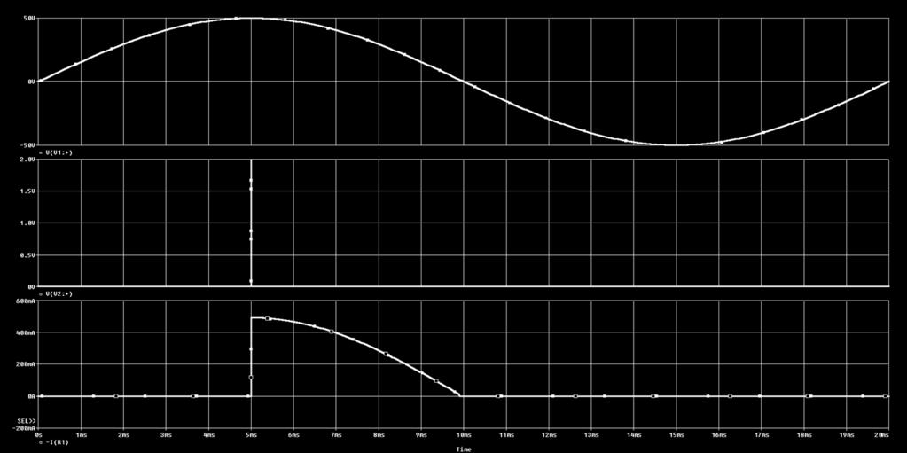
6 Power diodes Dynamic characteristics Reverse recovery: passing over from the conduction to the blocking state after a reverse voltage is applied. Forced: if the current reduction is too steep, after zero passaging, a certain amount of carriers change their direction thus making reverse conduction possible for a while: Storage time (t a ): time between zero crossing and the maximum reverse current. Fall time (t b ): time between maximum reverse current and its 25%. Reverse recovery time (t rr ): sum of the two previous ones. Recovery current (I rr ): peak current reached in this process. Natural: when the current reduction pace is low the previous parameters can be overlooked.

7 Forced reverse recovery Q rr I rr x t rr /2 Multimedia content available
8 Power diodes Dynamic characteristics Forward recovery: Turn-on process requires a certain time so the charge carriers can flood the depletion region. This creates a peak anode to cathode voltage. Forward recovery voltage. Forward recovery time: time necessary to stabilize anode to cathode conduction voltage. Forward recovery is a shorter phenomenon and provokes less power losses.

9 Bipolar power transistor - Introduction These BJT can conduct high currents and withstand high voltages. They frequently adopt a Darlington configuration to avoid the need for a high base current. The irruption of new devices has relegated BJTs to low and medium power ranges. In power applications transistors often work in cut-off and saturation regions thus avoiding the active one.

10 Power BJT Static characteristics In the cut-off region, base current has to be very low. To make collector current as low as possible and to impose the lowest possible collector to emitter voltage, the base terminal may be short circuited or even made slightly negative. o In cut-off region, collector current is very small although it grows slightly with the collector to emitter voltage. The transistor behaves approximately as an open circuit. In the saturation region, the base current has to be high enough. Collector to emitter voltage is low but increases proportionally to collector current. othe transistor behaves as a low value resistor, although ideally it should behave as a short circuit.
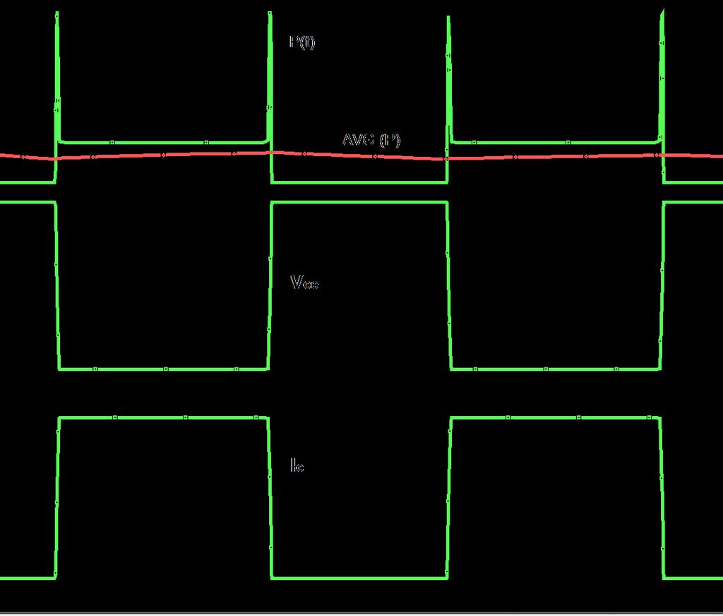
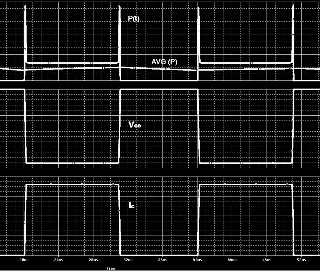
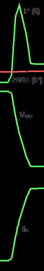
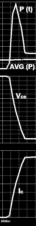
11 Power BJT Dynamic characteristics Parasitic capacities at the junctions and the charge carriers diffusion time at the base region cause the switch process (from cut-off to saturation and vice versa) not to be immediate. Delay time: since the base terminal is forwardly biased until the collector current reaches 10% of its final magnitude. Raise time: time the collector current lasts from 10% to 90% of its final value. Turn-on time: the two previous ones added together. Storage time: since the base terminal is unbiased until the collector current drops to 90% of its previous saturation value. Fall time: time taken by the collector current to fall from 90% to 10% of its previous saturation value. Turn-off time: the two previous ones added together. At both turn-on and turn-off significant current and voltage values coincide and provoke the appearance of power peaks. Average power loss will depend on the proximity of those peaks, that is, the operation frequency.
12
13 Power FET - Introduction They are FET capable of conducting high currents and withstanding high voltages. For this purpose they are given some constructive characteristics aimed to increase the base s influence and to reduce source to drain resistance. In power electronics transistors usually work in cut-off and saturation regions (switching), thus avoiding the active one. In power electronics enhancement devices are used.
14 Power FET Static characteristics Saturation is achieved applying a sufficient voltage to gate terminal so the channel is created. Source to drain voltage is low but increases proportionally to drain current. The transistor behaves as a low resistance although it should be ideally a short-circuit. Gate current is negligible. Cut-off is achieved by removing base voltage, which results in channel disappearance. Drain current is very low, lower than leakage current in bipolar transistors. Cut-off operation is very close to a perfect open circuit.

15 Power FET Static characteristics
16 Power FET Dynamic characteristics FETs switch faster than bipolar transistors due to the lack of minority charge carriers diffusion. The gate to source parasitic capacity poses a limit on the gate s voltage response to excitation, towards both cut-off and saturation: Delay time: since the base terminal is forwardly biased until the drain current reaches 10% of its final magnitude. Raise time: time the drain current lasts from 10% to 90% of its final value. Turn-on time: the two previous ones added together. Discharge (turn-off delay) time: since excitation is removed from the gate terminal until the drain current drops to 90% of its previous saturation value. Fall time: time taken by the drain current to fall from 90% to 10% of its previous saturation value. Turn-off time: the two previous ones added together. At both turn-on and turn-off significant current and voltage values coincide and provoke the appearance of power peaks. Average power loss will depend on the proximity of those peaks, that is, the operation frequency.
. From the constructive point of view it combines a FET, at its input (gate) with a bipolar at its output (collector to emitter). These are the names of its terminals.")
17 IGBT - Introduction Insulated Gate Bipolar Transistor (IGBT): this device aims to combine the advantages of the bipolar (low conduction losses) and FET (low excitation current and high switching speed). From the constructive point of view it combines a FET, at its input (gate) with a bipolar at its output (collector to emitter). These are the names of its terminals. Unlike the previous ones, it has no signal equivalent. Its behavior is similar to the FET s with the collector to emitter voltage axis displaced approximately one volt to the right (more collector to emitter voltage for the same collector current), with a more steep saturation curve (lower equivalent resistance).
18 IGBT Static characteristics In saturation region, the IGBT is affected by a higher collector to emitter voltage than the FET which however is offset by a lower equivalent resistance. In cut-off region it behaves very closely to a FET. Saturation losses are lower than a FET s, but higher than a bipolar s. A voltage gradient Vce provokes, through parasitic capacity C CG the appearance of a current that charges parasitic capacity C GE. If the voltage in this capacity, V GE, exceeds the MOS threshold voltage, the IGBT will undesirably turn on, which result in a loss of control and significant power losses.

19 IGBT Static characteristics
20 IGBT Dynamic characteristics IGBT s turn-on time is similar the FET s. Turn-off time is between the FET and the bipolar. Switch speed therefore is also between that of both devices but closer to the FET s. Power losses are also somewhere in between. All in all, the IGBT combines power and speed characteristics of both types of transistors, closer to the best case and therefore close to the goal of achieving the best of each one. An excessive voltage gradient would encounter trapped charges not totally evacuated. For this reason the maximum gradient allowed will be lower than if the device was in static condition.
21 Thyristor (SCR) - Introduction It is devoted only to power electronics applications. SCR (Silicon Controlled Rectifier): it works very much like a rectifier (diode), but a controlled one. Control terminal (gate) makes possible for an external circuit to put it on conduction state, provided a positive and sufficient anode cathode voltage is applied.
22 Thyristor (SCR) Static characteristics cut off The thyristor is in cut-off condition when: Anode cathode voltage is positive but gate voltage referred to ground is not positive (direct cut-off). Anode cathode voltage is negative (reverse blocking) regardless of gate s condition. In blocking state only the leakage current is present. It grows slightly as anode cathode voltage does and more significantly as temperature rises. In direct blocking state it may reach the direct breakout current and turn the device to condition without any damage. Voltage parameters are analogous to the diode s but affecting both direct and reverse situations: Maximum DC reverse/direct voltage:. Maximum reverse/direct repetitive voltage. Peak reverse/direct voltage. Breakdown reverse/direct voltage.
.")
23 Thyristor (SCR) Static characteristics conduction Anode s current is imposed by external circuit (it is not related to the gate) and must be kept over the to prevent spontaneous blocking. Anode to cathode voltage is kept around 1 5 2V. Working parameters are analogous to the diode s: Maximum average forward current (it can also be expressed in terms of rms current). Maximum peak repetitive current. Maximum peak current. Conduction losses: PP cc = 1,3 II AAAA + rrii AA 2 1,3V: voltage drop. I Am : anode s average current. r: dynamic thyristor s resistance. I A : anode s rms current.
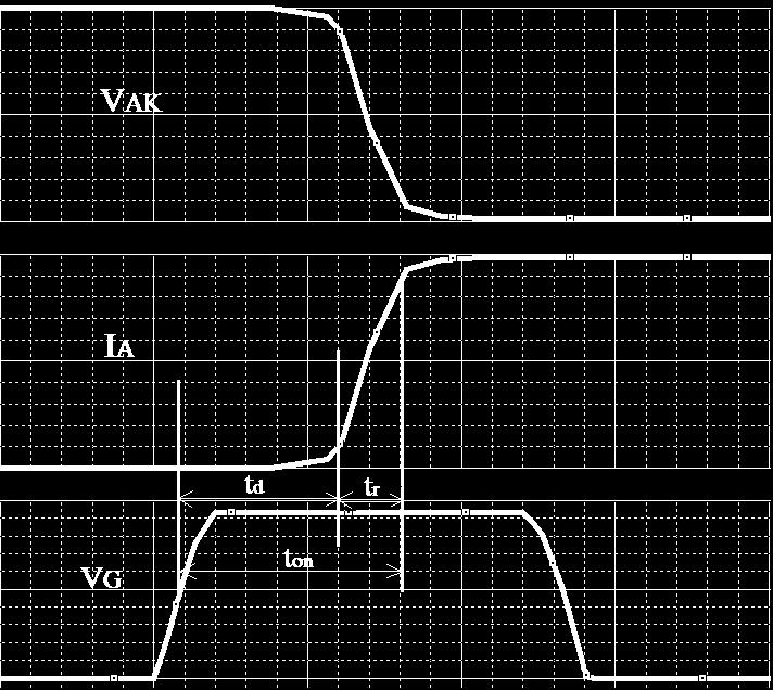
24 Thyristor (SCR) Switching When switched on the thyristor shifts from direct blocking to conduction and remains in that condition. Accidental trigger: Due to overvoltage: an excessive anode cathode direct voltage may cause the current to reach its breakout value. Due to voltage gradient: anode cathode voltage may put the device in conduction state even if it is not high provided it is applied rapidly. The required positive slope dv AK /dt depends on the final voltage and external temperature (less gradient is needed as these two magnitudes increase). It is usually given in terms of (dv AK /dt) máx for a given final voltage value (2/3 maximum direct repetitive voltage). Switching by gate pulse: it is the usual switching procedure. An electrical pulse is provided on the gate terminal (when anode cathode voltage is positive). Delay time (t d ): since the pulse is applied to the gate terminal until anode s current reaches 10% of its final value. Rise time (t r ): from 10% to 90% of on state current. Turn on delay time (t on ): the sum of both. At the moment of switch on, anode s current slope must not exceed a certain value (di A /dt) máx. This is so because right after switch on the current is restricted to a small fraction of the pn junction, close to the gate terminal. As a consequence, a temporarily high current density may damage the device.
25
26 Thyristor (SCR) Triggering characteristics. The pulses delivered to the gate terminal must comply with several requirements to ensure turn on. : Pulse width must be long enough to allow the anode s current to reach its holding current value (I H ). Latching current / gate trigger current (I GT ) is the minimum gate current that guarantees turn on at working temperature. Gate cathode voltage must be above the gate trigger voltage (V GT ) at working temperature. Actually this voltage produces the former current value thus ensuring trigger. In order to avoid accidental turn-on, vendors provide: Gate non-trigger voltage (V GD ). Gate non-trigger current (I GD ). To recap: A voltage/current value above the trigger one ensures turn-on. When both voltage and current are below the non-trigger values an unwanted trigger will not occur. In any other scenario the result is uncertain.
27
28 Thyristor (SCR) Blocking Blocking the thyristor through the gate terminal is not possible. When anode current drops below its holding value (I H ) natural blocking occurs. When the reduction pace (di A /dt) is too high, the thyristor may end up conducting negative current exactly like diodes do. Turn-off time (t q ): elapsed time since current has gone to cero (or negative) until a positive anode to cathode voltage can not turn on the device without trigger impulse. Blocking can be forced on the thyristor: By means of a sufficient reverse anode to cathode voltage. By means of a current source opposed to the direct anode current.

29 MCT (MOS Controlled Thyristor) It is a hybrid device similarly to the IGBT. It is composed of two MOS transistors. One of them is meant to turn on the device whilst the other one turns it off. In this case the reference terminal is the anode. When in direct blocking a negative anode to gate voltage turns the MCT on. When conducting a positive gate to anode voltage turns it off. Turn off is only possible when current is below the so called peak controllable current. Above this an attempt to turn the MCT off may destroy it. In that case the MCT behaves as any other thyristor. The width of the triggering pulses on the gate terminal depends on the current. It is recommended to maintain the pulses throughout the whole conduction/blocking period. It is made up from multiple parallel cells in parallel so it can withstand higher current gradients.
30 Other devices GTO: Gate turn-off thyristor. A thyristor that can be turned off from the gate terminal. DIAC: a self protecting device that conducts both positive and negative current when breakdown voltage is reached. TRIAC: a DIAC with a control terminal to turn it on in any current sense before it reaches the breakdown voltage. Hybrid devices: apart from IGBT and MCT there are many other hybrid devices with similar characteristics.
31 References Electrónica de Potencia. Salvador M. García, Juan A. Gualda Gil. Thomson Editores Spain, Paraninfo S.A., 2006 Thyristor Theory and Design Considerations. Handbook. HBD855/D Rev. 1, Nov ON Semiconductor
Power Electronics Power semiconductor devices. Dr. Firas Obeidat
 Power Electronics Power semiconductor devices Dr. Firas Obeidat 1 Table of contents 1 Introduction 2 Classifications of Power Switches 3 Power Diodes 4 Thyristors (SCRs) 5 The Triac 6 The Gate Turn-Off
Power Semiconductor Devices
 TRADEMARK OF INNOVATION Power Semiconductor Devices Introduction This technical article is dedicated to the review of the following power electronics devices which act as solid-state switches in the circuits.
2 Marks - Question Bank. Unit 1- INTRODUCTION
 Two marks 1. What is power electronics? EE6503 POWER ELECTRONICS 2 Marks - Question Bank Unit 1- INTRODUCTION Power electronics is a subject that concerns the applications electronics principles into situations
Chapter 8. Field Effect Transistor
 Chapter 8. Field Effect Transistor Field Effect Transistor: The field effect transistor is a semiconductor device, which depends for its operation on the control of current by an electric field. There
THE JFET. Script. Discuss the JFET and how it differs from the BJT. Describe the basic structure of n-channel and p -channel JFETs
 Course: B.Sc. Applied Physical Science (Computer Science) Year & Sem.: Ist Year, Sem - IInd Subject: Electronics Paper No.: V Paper Title: Analog Circuits Lecture No.: 12 Lecture Title: Analog Circuits
Power Electronics. P. T. Krein
 Power Electronics Day 10 Power Semiconductor Devices P. T. Krein Department of Electrical and Computer Engineering University of Illinois at Urbana-Champaign 2011 Philip T. Krein. All rights reserved.
Teccor brand Thyristors AN1001
 A1001 Introduction The Thyristor family of semiconductors consists of several very useful devices. The most widely used of this family are silicon controlled rectifiers (SCRs), Triacs, SIDACs, and DIACs.
Analog and Telecommunication Electronics
 Politecnico di Torino - ICT School Analog and Telecommunication Electronics F2 Active power devices»mos»bjt» IGBT, TRIAC» Safe Operating Area» Thermal analysis 30/05/2012-1 ATLCE - F2-2011 DDC Lesson F2:
Switching and Semiconductor Switches
 1 Switching and Semiconductor Switches 1.1 POWER FLOW CONTROL BY SWITCHES The flow of electrical energy between a fixed voltage supply and a load is often controlled by interposing a controller, as shown
Solid State Devices- Part- II. Module- IV
 Solid State Devices- Part- II Module- IV MOS Capacitor Two terminal MOS device MOS = Metal- Oxide- Semiconductor MOS capacitor - the heart of the MOSFET The MOS capacitor is used to induce charge at the
UNIT 3: FIELD EFFECT TRANSISTORS
 FIELD EFFECT TRANSISTOR: UNIT 3: FIELD EFFECT TRANSISTORS The field effect transistor is a semiconductor device, which depends for its operation on the control of current by an electric field. There are
SRM INSTITUTE OF SCIENCE AND TECHNOLOGY (DEEMED UNIVERSITY)
") SRM INSTITUTE OF SCIENCE AND TECHNOLOGY (DEEMED UNIVERSITY) QUESTION BANK I YEAR B.Tech (II Semester) ELECTRONIC DEVICES (COMMON FOR EC102, EE104, IC108, BM106) UNIT-I PART-A 1. What are intrinsic and
SRM INSTITUTE OF SCIENCE AND TECHNOLOGY (DEEMED UNIVERSITY) QUESTION BANK I YEAR B.Tech (II Semester) ELECTRONIC DEVICES (COMMON FOR EC102, EE104, IC108, BM106) UNIT-I PART-A 1. What are intrinsic and
UNIT I POWER SEMI-CONDUCTOR DEVICES
 UNIT I POWER SEMI-CONDUCTOR DEVICES SUBJECT CODE SUBJECT NAME STAFF NAME : EE6503 : Power Electronics : Ms.M.Uma Maheswari 1 SEMICONDUCTOR DEVICES POWER DIODE POWER TRANSISTORS POWER BJT POWER MOSFET IGBT
EEL 5245 POWER ELECTRONICS I Lecture #4: Chapter 2 Switching Concepts and Semiconductor Overview
 EEL 5245 POWER ELECTRONICS I Lecture #4: Chapter 2 Switching Concepts and Semiconductor Overview Objectives of Lecture Switch realizations Objective is to focus on terminal characteristics Blocking capability
Today s subject MOSFET and IGBT
 Today s subject MOSFET and IGBT 2018-05-22 MOSFET metal oxide semiconductor field effect transistor Drain Gate n-channel Source p-channel The MOSFET - Source Gate G D n + p p n + S body body n - drift
CHAPTER I INTRODUCTION
 CHAPTER I INTRODUCTION High performance semiconductor devices with better voltage and current handling capability are required in different fields like power electronics, computer and automation. Since
Questions on JFET: 1) Which of the following component is a unipolar device?
 Which of the following component is a unipolar device?") Questions on JFET: 1) Which of the following component is a unipolar device? a) BJT b) FET c) DJT d) EFT 2) Current Conduction in FET takes place due e) Majority charge carriers only f) Minority charge
Questions on JFET: 1) Which of the following component is a unipolar device? a) BJT b) FET c) DJT d) EFT 2) Current Conduction in FET takes place due e) Majority charge carriers only f) Minority charge
DOWNLOAD PDF POWER ELECTRONICS DEVICES DRIVERS AND APPLICATIONS
 Chapter 1 : Power Electronics Devices, Drivers, Applications, and Passive theinnatdunvilla.com - Google D Download Power Electronics: Devices, Drivers and Applications By B.W. Williams - Provides a wide
Introduction to Power Electronics BACKGROUND
 Department of Electrical Drives and Power Electronics Introduction to Power Electronics BACKGROUND Valery Vodovozov and Zoja Raud Tallinn 2010 Contents Preface... 3 Historical background... 4 Power electronic
Prof. Steven S. Saliterman Introductory Medical Device Prototyping
 Introductory Medical Device Prototyping Department of Biomedical Engineering, University of Minnesota http://saliterman.umn.edu/ Solid state power switching: Silicon controlled rectifiers (SCR or Thyristor).
Reg. No. : Question Paper Code : B.E./B.Tech. DEGREE EXAMINATION, NOVEMBER/DECEMBER Second Semester
 WK 5 Reg. No. : Question Paper Code : 27184 B.E./B.Tech. DEGREE EXAMINATION, NOVEMBER/DECEMBER 2015. Time : Three hours Second Semester Electronics and Communication Engineering EC 6201 ELECTRONIC DEVICES
Pre-certification Electronics Questions. Answer the following with the MOST CORRECT answer.
 Electronics Questions Answer the following with the MOST CORRECT answer. 1. The cathode end terminal of a semiconductor diode can be identified by: a. the negative sign marked on the case b. a circular
SCR- SILICON CONTROLLED RECTIFIER
 SCR- SILICON CONTROLLED RECTIFIER Definition: When a pn junction is added to a junction transistor, the resulting three pn junction device is called a silicon controlled rectifier. SCR can change alternating
 http://www.electronics-tutorials.ws/power/triac.html Triac Tutorial and Basic Principles In the previous tutorial we looked at the construction and operation of the Silicon Controlled Rectifier more commonly
Basic Electronics Prof. T.S. Natarajan Department of Physics Indian Institute of Technology, Madras
 Basic Electronics Prof. T.S. Natarajan Department of Physics Indian Institute of Technology, Madras Lecture 39 Silicon Controlled Rectifier (SCR) (Construction, characteristics (Dc & Ac), Applications,
Chapter 1 Power Electronic Devices
 Chapter 1 Power Electronic Devices Outline 1.1 An introductory overview of power electronic devices 1.2 Uncontrolled device power diode 1.3 Half- controlled device thyristor 1.4 Typical fully- controlled
AN1001. Fundamental Characteristics of Thyristors. Introduction. Basic Operation of a Triac. Basic Operation of an SCR. Basic Operation of a Diac
 A1001 Fundamental Characteristics of Thyristors 14 Introduction The thyristor family of semiconductors consists of several very useful devices. The most widely used of this family are silicon controlled
UNIT 3 Transistors JFET
 UNIT 3 Transistors JFET Mosfet Definition of BJT A bipolar junction transistor is a three terminal semiconductor device consisting of two p-n junctions which is able to amplify or magnify a signal. It
Lecture Switching Characteristics (Dynamic characteristics) Fig. 3.7 : Turn - on characteristics
 Fig. 3.7 : Turn - on characteristics") Lecture-14 3.4 Switching Characteristics (Dynamic characteristics) Thyristor Turn-ON Characteristics Fig. 3.7 : Turn - on characteristics When the SCR is turned on with the application of the gate signal,
Lecture-14 3.4 Switching Characteristics (Dynamic characteristics) Thyristor Turn-ON Characteristics Fig. 3.7 : Turn - on characteristics When the SCR is turned on with the application of the gate signal,
Lecture Note on Switches Marc T. Thompson, 2003 Revised Use with gratefulness for ECE 3503 B term 2018 WPI Tan Zhang
 Lecture Note on Switches Marc T. Thompson, 2003 Revised 2007 Use with gratefulness for ECE 3503 B term 2018 WPI Tan Zhang Lecture note on switches_tan_thompsonpage 1 of 21 1. DEVICES OVERVIEW... 4 1.1.
Fundamentals of Power Semiconductor Devices
 В. Jayant Baliga Fundamentals of Power Semiconductor Devices 4y Spri ringer Contents Preface vii Chapter 1 Introduction 1 1.1 Ideal and Typical Power Switching Waveforms 3 1.2 Ideal and Typical Power Device
Difference between BJTs and FETs. Junction Field Effect Transistors (JFET)
") Difference between BJTs and FETs Transistors can be categorized according to their structure, and two of the more commonly known transistor structures, are the BJT and FET. The comparison between BJTs
Difference between BJTs and FETs Transistors can be categorized according to their structure, and two of the more commonly known transistor structures, are the BJT and FET. The comparison between BJTs
Intelligent Semiconductor Analyzer User Manual
 Intelligent Semiconductor Analyzer User Manual Please read this manual before switching the unit on. Important safety information inside. 2 Contents Page 1.Introduction... 4 2.Important Considerations...
Electrical Engineering EE / EEE. Postal Correspondence Course. Power Electronics. GATE, IES & PSUs
 Power Electronics-EE GATE, IES, PSU 1 SAMPLE STUDY MATERIAL Electrical Engineering EE / EEE Postal Correspondence Course Power Electronics GATE, IES & PSUs Power Electronics-EE GATE, IES, PSU 2 C O N T
Diodes and Applications
 Diodes and Applications Diodes and Applications 2 1 Diode Operation 2 2 Voltage-Current (V-I) Characteristics 2 3 Diode Models 2 4 Half-Wave Rectifiers 2 5 Full-Wave Rectifiers 2 6 Power Supply Filters
The Gate Turn-Off Thyristors (GTO) Part 2
 Part 2") The Gate Turn-Off Thyristors (GTO) Part 2 Static Characteristics On-state Characteristics: In the on-state the GTO operates in a similar manner to the thyristor. If the anode current remains above the
The Gate Turn-Off Thyristors (GTO) Part 2 Static Characteristics On-state Characteristics: In the on-state the GTO operates in a similar manner to the thyristor. If the anode current remains above the
IFB270 Advanced Electronic Circuits
 IFB270 Advanced Electronic Circuits Chapter 11: Thyristors Prof. Manar Mohaisen Department of EEC Engineering Review of the Precedent Lecture To introduce several concepts on capacitance in amplifiers
Field-Effect Transistor (FET) is one of the two major transistors; FET derives its name from its working mechanism;
 is one of the two major transistors; FET derives its name from its working mechanism;") Chapter 3 Field-Effect Transistors (FETs) 3.1 Introduction Field-Effect Transistor (FET) is one of the two major transistors; FET derives its name from its working mechanism; The concept has been known
Chapter 3 Field-Effect Transistors (FETs) 3.1 Introduction Field-Effect Transistor (FET) is one of the two major transistors; FET derives its name from its working mechanism; The concept has been known
Analysis on IGBT Developments
 Analysis on IGBT Developments Mahato G.C., Niranjan and Waquar Aarif Abu RVS College of Engineering and Technology, Jamshedpur India Abstract Silicon based high power devices continue to play an important
Semiconductor analyser AS4002P User Manual
 Semiconductor analyser AS4002P User Manual Copyright Ormelabs (C) 2010 http://www.ormelabs.com 1 CONTENTS SECTION Page SECTION 1: Introduction... 3 SECTION 2: Features... 3 SECTION 3: Component analysis...
Reading. Lecture 17: MOS transistors digital. Context. Digital techniques:
 Reading Lecture 17: MOS transistors digital Today we are going to look at the analog characteristics of simple digital devices, 5. 5.4 And following the midterm, we will cover PN diodes again in forward
CHAPTER 8 FIELD EFFECT TRANSISTOR (FETs)
") CHAPTER 8 FIELD EFFECT TRANSISTOR (FETs) INTRODUCTION - FETs are voltage controlled devices as opposed to BJT which are current controlled. - There are two types of FETs. o Junction FET (JFET) o Metal
CHAPTER 8 FIELD EFFECT TRANSISTOR (FETs) INTRODUCTION - FETs are voltage controlled devices as opposed to BJT which are current controlled. - There are two types of FETs. o Junction FET (JFET) o Metal
(Refer Slide Time: 02:05)
") Electronics for Analog Signal Processing - I Prof. K. Radhakrishna Rao Department of Electrical Engineering Indian Institute of Technology Madras Lecture 27 Construction of a MOSFET (Refer Slide Time:
Electronics for Analog Signal Processing - I Prof. K. Radhakrishna Rao Department of Electrical Engineering Indian Institute of Technology Madras Lecture 27 Construction of a MOSFET (Refer Slide Time:
Power Electronics. Lecture No - 8
 Power Electronics Prof. B.G. Fernandes Department of Electrical Engineeringg Indian Institute of Technology, Bombay Lecture No - 8 Hello, in my last class we discussed the operation of bipolar junctionn
I E I C since I B is very small
 Figure 2: Symbols and nomenclature of a (a) npn and (b) pnp transistor. The BJT consists of three regions, emitter, base, and collector. The emitter and collector are usually of one type of doping, while
Chapter 3: TRANSISTORS. Dr. Gopika Sood PG Govt. College For Girls Sector -11, Chandigarh
 Chapter 3: TRANSISTORS Dr. Gopika Sood PG Govt. College For Girls Sector -11, Chandigarh OUTLINE Transistors Bipolar Junction Transistor (BJT) Operation of Transistor Transistor parameters Load Line Biasing
UNIT I PN JUNCTION DEVICES
 UNIT I PN JUNCTION DEVICES 1. Define Semiconductor. 2. Classify Semiconductors. 3. Define Hole Current. 4. Define Knee voltage of a Diode. 5. What is Peak Inverse Voltage? 6. Define Depletion Region in
(anode) (also: I D, I F, I T )
 (also: I D, I F, I T )") (anode) V R - V A or V D or VF or V T IA (also: I D, I F, I T ) control terminals (e.g. gate for thyrisr; basis for BJT) - (IR =-I A ) (cathode) I A I F conducting range A p n K (a) V A (V F ) - A anode
(anode) V R - V A or V D or VF or V T IA (also: I D, I F, I T ) control terminals (e.g. gate for thyrisr; basis for BJT) - (IR =-I A ) (cathode) I A I F conducting range A p n K (a) V A (V F ) - A anode
UNIT II JFET, MOSFET, SCR & UJT
 UNIT II JFET, MOSFET, SCR & UJT JFET JFET as an Amplifier and its Output Characteristics JFET Applications MOSFET Working Principles, SCR Equivalent Circuit and V-I Characteristics. SCR as a Half wave
Battery Charger Circuit Using SCR
 Battery Charger Circuit Using SCR Introduction to SCR: SCR is abbreviation for Silicon Controlled Rectifier. SCR has three pins anode, cathode and gate as shown in the below figure. It is made up of there
AE53/AC53/AT53/AE103 ELECT. DEVICES & CIRCUITS DEC 2015
 Q.2 a. By using Norton s theorem, find the current in the load resistor R L for the circuit shown in Fig.1. (8) Fig.1 IETE 1 b. Explain Z parameters and also draw an equivalent circuit of the Z parameter
QUESTION BANK EC6201 ELECTRONIC DEVICES UNIT I SEMICONDUCTOR DIODE PART A. It has two types. 1. Intrinsic semiconductor 2. Extrinsic semiconductor.
 FATIMA MICHAEL COLLEGE OF ENGINEERING & TECHNOLOGY Senkottai Village, Madurai Sivagangai Main Road, Madurai - 625 020. [An ISO 9001:2008 Certified Institution] QUESTION BANK EC6201 ELECTRONIC DEVICES SEMESTER:
EE 330 Lecture 27. Bipolar Processes. Special Bipolar Processes. Comparison of MOS and Bipolar Proces JFET. Thyristors SCR TRIAC
 EE 330 Lecture 27 Bipolar Processes Comparison of MOS and Bipolar Proces JFET Special Bipolar Processes Thyristors SCR TRIAC Review from a Previous Lecture B C E E C vertical npn B A-A Section B C E C
Chapter 1 INTRODUCTION TO POWER ELECTRONICS SYSTEMS
 Chapter 1 INTRODUCTION TO POWER ELECTRONICS SYSTEMS Definition and concepts Application Power semiconductor switches Gate/base drivers Losses Snubbers 1 Definition of Power Electronics DEFINITION: To convert,
UNIT-VI FIELD EFFECT TRANSISTOR. 1. Explain about the Field Effect Transistor and also mention types of FET s.
 UNIT-I FIELD EFFECT TRANSISTOR 1. Explain about the Field Effect Transistor and also mention types of FET s. The Field Effect Transistor, or simply FET however, uses the voltage that is applied to their
Shankersinh Vaghela Bapu Institute of Technology INDEX
 Shankersinh Vaghela Bapu Institute of Technology Diploma EE Semester III 3330905: ELECTRONIC COMPONENTS AND CIRCUITS INDEX Sr. No. Title Page Date Sign Grade 1 Obtain I-V characteristic of Diode. 2 To
EIE209 Basic Electronics. Transistor Devices. Contents BJT and FET Characteristics Operations. Prof. C.K. Tse: T ransistor devices
 EIE209 Basic Electronics Transistor Devices Contents BJT and FET Characteristics Operations 1 What is a transistor? Three-terminal device whose voltage-current relationship is controlled by a third voltage
3. Draw the two transistor model of a SCR and mention its applications. (MAY 2016)
") DHANALAKSHMI COLLEGE OF ENGINEERING DEPARTMENT OF ELECTRICAL AND ELECTRONICS ENGINEERING EE6503 POWER ELECTRONICS UNIT I- POWER SEMI-CONDUCTOR DEVICES PART - A 1. What is a SCR? A silicon-controlled rectifier
DHANALAKSHMI COLLEGE OF ENGINEERING DEPARTMENT OF ELECTRICAL AND ELECTRONICS ENGINEERING EE6503 POWER ELECTRONICS UNIT I- POWER SEMI-CONDUCTOR DEVICES PART - A 1. What is a SCR? A silicon-controlled rectifier
Lecture 3: Transistors
 Lecture 3: Transistors Now that we know about diodes, let s put two of them together, as follows: collector base emitter n p n moderately doped lightly doped, and very thin heavily doped At first glance,
 VALLIAMMAI ENGINEERING COLLEGE SRM NAGAR, KATTANKULATHUR- 603 203 DEPARTMENT OF ELECTRONICS AND COMMUNICATION ENGINEERING EC6202- ELECTRONIC DEVICES AND CIRCUITS UNIT I PN JUNCTION DEVICES 1. Define Semiconductor.
The Common Source JFET Amplifier
 The Common Source JFET Amplifier Small signal amplifiers can also be made using Field Effect Transistors or FET's for short. These devices have the advantage over bipolar transistors of having an extremely
Basic Electronics Prof. Dr. Chitralekha Mahanta Department of Electronics and Communication Engineering Indian Institute of Technology, Guwahati
 Basic Electronics Prof. Dr. Chitralekha Mahanta Department of Electronics and Communication Engineering Indian Institute of Technology, Guwahati Module: 3 Field Effect Transistors Lecture-7 High Frequency
1 Basics V GG. V GS(th) V GE(th) , i C. i D I L. v DS. , v CE V DD V CC. V DS(on) VCE(sat) (IGBT) I t MOSFET MOSFET.
 V GE(th) , i C. i D I L. v DS. , v CE V DD V CC. V DS(on) VCE(sat) (IGBT) I t MOSFET MOSFET.") Reverse operation During reverse operation (Figure 1.10, III rd quadrant) the IGBT collector pn-junction is poled in reverse direction and there is no inverse conductivity, other than with MOSFETs. Although,
Reverse operation During reverse operation (Figure 1.10, III rd quadrant) the IGBT collector pn-junction is poled in reverse direction and there is no inverse conductivity, other than with MOSFETs. Although,
Fundamentals of Microelectronics
 Fundamentals of Microelectronics CH1 Why Microelectronics? CH2 Basic Physics of Semiconductors CH3 Diode Circuits CH4 Physics of Bipolar Transistors CH5 Bipolar Amplifiers CH6 Physics of MOS Transistors
CHAPTER 1 DIODE CIRCUITS. Semiconductor act differently to DC and AC currents
 CHAPTER 1 DIODE CIRCUITS Resistance levels Semiconductor act differently to DC and AC currents There are three types of resistances 1. DC or static resistance The application of DC voltage to a circuit
Unijunction Transistor. T.Y.B.Sc - Eletronics POWER ELETRONICS
 Unijunction Transistor T.Y.B.Sc - Eletronics POWER ELETRONICS Unijunction Transistor Symbol and Construction The Unijunction Transistor is solid state three terminal device that can be used in gate pulse,
Field Effect Transistors (npn)
") Field Effect Transistors (npn) gate drain source FET 3 terminal device channel e - current from source to drain controlled by the electric field generated by the gate base collector emitter BJT 3 terminal
Field Effect Transistors (npn) gate drain source FET 3 terminal device channel e - current from source to drain controlled by the electric field generated by the gate base collector emitter BJT 3 terminal
FIELD EFFECT TRANSISTOR (FET) 1. JUNCTION FIELD EFFECT TRANSISTOR (JFET)
 1. JUNCTION FIELD EFFECT TRANSISTOR (JFET)") FIELD EFFECT TRANSISTOR (FET) The field-effect transistor (FET) is a three-terminal device used for a variety of applications that match, to a large extent, those of the BJT transistor. Although there
FIELD EFFECT TRANSISTOR (FET) The field-effect transistor (FET) is a three-terminal device used for a variety of applications that match, to a large extent, those of the BJT transistor. Although there
Grade of climate describes the permissible ambient test conditions (climate) according to DIN IEC 68-1
 according to DIN IEC 68-1") Total power dissipation P tot Maximum power dissipation per transistor/ diode or within the whole power module P tot = (T jmax -T case )/R thjc, Parameter: case temperature T case = 25 C Operating temperature
Total power dissipation P tot Maximum power dissipation per transistor/ diode or within the whole power module P tot = (T jmax -T case )/R thjc, Parameter: case temperature T case = 25 C Operating temperature
BJT. Bipolar Junction Transistor BJT BJT 11/6/2018. Dr. Satish Chandra, Assistant Professor, P P N College, Kanpur 1
 BJT Bipolar Junction Transistor Satish Chandra Assistant Professor Department of Physics P P N College, Kanpur www.satish0402.weebly.com The Bipolar Junction Transistor is a semiconductor device which
Unit III FET and its Applications. 2 Marks Questions and Answers
 Unit III FET and its Applications 2 Marks Questions and Answers 1. Why do you call FET as field effect transistor? The name field effect is derived from the fact that the current is controlled by an electric
7. Bipolar Junction Transistor
 41 7. Bipolar Junction Transistor 7.1. Objectives - To experimentally examine the principles of operation of bipolar junction transistor (BJT); - To measure basic characteristics of n-p-n silicon transistor
LESSON PLAN. Chap.no. Testing. & Page. Outcome No. 1. Introduction - T1 C5,95. Understand the devices. a).an ability to 2. Field intensity - potential
.an ability to 2. Field intensity - potential") EE0207 ELECTRONIC DEVICES LESSON PLAN SEMICONDUCTORS Semiconductors devices: Field intensity - potential energy - mobility - conductivity - electrons holes - charge density in semiconductors - electrical
EE0207 ELECTRONIC DEVICES LESSON PLAN SEMICONDUCTORS Semiconductors devices: Field intensity - potential energy - mobility - conductivity - electrons holes - charge density in semiconductors - electrical
Lecture 2 - Overview of power switching devices. The Power Switch: what is a good power switch?
 Lecture 2 - Overview of power switching devices The Power Switch: what is a good power switch? A K G Attributes of a good power switch are: 1. No power loss when ON 2. No power loss when OFF 3. No power
UNIVERSITY OF CALIFORNIA AT BERKELEY College of Engineering Department of Electrical Engineering and Computer Sciences.
 UNIVERSITY OF CALIFORNIA AT BERKELEY College of Engineering Department of Electrical Engineering and Computer Sciences Discussion #9 EE 05 Spring 2008 Prof. u MOSFETs The standard MOSFET structure is shown
1. Introduction Device structure and operation Structure Operation...
 Application Note 96 February, 2 IGBT Basics by K.S. Oh CONTENTS. Introduction... 2. Device structure and operation... 2-. Structure... 2-2. Operation... 3. Basic Characteristics... 3-. Advantages, Disadvantages
the reactance of the capacitor, 1/2πfC, is equal to the resistance at a frequency of 4 to 5 khz.
 EXPERIMENT 12 INTRODUCTION TO PSPICE AND AC VOLTAGE DIVIDERS OBJECTIVE To gain familiarity with PSPICE, and to review in greater detail the ac voltage dividers studied in Experiment 14. PROCEDURE 1) Connect
This chapter describes precautions for actual operation of the IGBT module.
 Chapter 5 Precautions for Use 1. Maximum Junction Temperature T vj(max) 5-2 2. Short-Circuit Protection 5-2 3. Over Voltage Protection and Safety Operation Area 5-2 4. Operation Condition and Dead time
BJT Amplifier. Superposition principle (linear amplifier)
") BJT Amplifier Two types analysis DC analysis Applied DC voltage source AC analysis Time varying signal source Superposition principle (linear amplifier) The response of a linear amplifier circuit excited
BJT Amplifier Two types analysis DC analysis Applied DC voltage source AC analysis Time varying signal source Superposition principle (linear amplifier) The response of a linear amplifier circuit excited
Fundamentals of Microelectronics
 Fundamentals of Microelectronics CH1 Why Microelectronics? CH2 Basic Physics of Semiconductors CH3 Diode Circuits CH4 Physics of Bipolar Transistors CH5 Bipolar Amplifiers CH6 Physics of MOS Transistors
Fig. 1 - Enhancement mode GaN has a circuiut schematic similar to silicon MOSFETs with Gate (G), Drain (D), and Source (S).
, Drain (D), and Source (S).") GaN Basics: FAQs Sam Davis; Power Electronics Wed, 2013-10-02 Gallium nitride transistors have emerged as a high-performance alternative to silicon-based transistors, thanks to the technology's ability
GaN Basics: FAQs Sam Davis; Power Electronics Wed, 2013-10-02 Gallium nitride transistors have emerged as a high-performance alternative to silicon-based transistors, thanks to the technology's ability
Dr.Arkan A.Hussein Power Electronics Fourth Class. Commutation of Thyristor-Based Circuits Part-I
 Commutation of Thyristor-Based Circuits Part-I ١ This lesson provides the reader the following: (i) (ii) (iii) (iv) Requirements to be satisfied for the successful turn-off of a SCR The turn-off groups
Understanding MOSFET Data. Type of Channel N-Channel, or P-Channel. Design Supertex Family Number TO-243AA (SOT-89) Die
 Die") Understanding MOSFET Data Application Note The following outline explains how to read and use Supertex MOSFET data sheets. The approach is simple and care has been taken to avoid getting lost in a maze
Understanding MOSFET Data Application Note The following outline explains how to read and use Supertex MOSFET data sheets. The approach is simple and care has been taken to avoid getting lost in a maze
Insulated Gate Bipolar Transistor (IGBT)
") nsulated Gate Bipolar Transistor (GBT) Comparison between BJT and MOS power devices: BJT MOS pros cons pros cons low V O thermal instability thermal stability high R O at V MAX > 400 V high C current complex
nsulated Gate Bipolar Transistor (GBT) Comparison between BJT and MOS power devices: BJT MOS pros cons pros cons low V O thermal instability thermal stability high R O at V MAX > 400 V high C current complex
Electronic Circuits II - Revision
 Electronic Circuits II - Revision -1 / 16 - T & F # 1 A bypass capacitor in a CE amplifier decreases the voltage gain. 2 If RC in a CE amplifier is increased, the voltage gain is reduced. 3 4 5 The load
Field - Effect Transistor
 Page 1 of 6 Field - Effect Transistor Aim :- To draw and study the out put and transfer characteristics of the given FET and to determine its parameters. Apparatus :- FET, two variable power supplies,
MTLE-6120: Advanced Electronic Properties of Materials. Semiconductor transistors for logic and memory. Reading: Kasap
 MTLE-6120: Advanced Electronic Properties of Materials 1 Semiconductor transistors for logic and memory Reading: Kasap 6.6-6.8 Vacuum tube diodes 2 Thermionic emission from cathode Electrons collected
Module 04.(B1) Electronic Fundamentals
 Electronic Fundamentals") 1.1a. Semiconductors - Diodes. Module 04.(B1) Electronic Fundamentals Question Number. 1. What gives the colour of an LED?. Option A. The active element. Option B. The plastic it is encased in. Option
1.1a. Semiconductors - Diodes. Module 04.(B1) Electronic Fundamentals Question Number. 1. What gives the colour of an LED?. Option A. The active element. Option B. The plastic it is encased in. Option
Basic Electronics: Diodes and Transistors. October 14, 2005 ME 435
 Basic Electronics: Diodes and Transistors Eşref Eşkinat E October 14, 2005 ME 435 Electric lectricity ity to Electronic lectronics Electric circuits are connections of conductive wires and other devices
semiconductor p-n junction Potential difference across the depletion region is called the built-in potential barrier, or built-in voltage:
 Chapter four The Equilibrium pn Junction The Electric field will create a force that will stop the diffusion of carriers reaches thermal equilibrium condition Potential difference across the depletion
EC 307 Power Electronics & Instrumentation
 EC 307 Power Electronics & Instrumentation MODULE I Difference Between Linear Electronics and Power Electronics Electronics has now become the core component in the development of the technology. The fast
Diode Characteristics and Applications
 Diode Characteristics and Applications Topics covered in this presentation: Diode Characteristics Diode Clamp Protecting Against Back-EMF Half-Wave Rectifier The Zener Diode 1 of 18 Diode Characteristics
Term Roadmap : Materials Types 1. INSULATORS
 Term Roadmap : Introduction to Signal Processing Differentiating and Integrating Circuits (OpAmps) Clipping and Clamping Circuits(Diodes) Design of analog filters Sinusoidal Oscillators Multivibrators
Transistor Characteristics
 Transistor Characteristics Introduction Transistors are the most recent additions to a family of electronic current flow control devices. They differ from diodes in that the level of current that can flow
Electro - Principles I
 The PN Junction Diode Introduction to the PN Junction Diode Note: In this chapter we consider conventional current flow. Page 11-1 The schematic symbol for the pn junction diode the shown in Figure 1.
UNIT IX ELECTRONIC DEVICES
 UNT X ELECTRONC DECES Weightage Marks : 07 Semiconductors Semiconductors diode-- characteristics in forward and reverse bias, diode as rectifier. - characteristics of LED, Photodiodes, solarcell and Zener
Mechatronics and Measurement. Lecturer:Dung-An Wang Lecture 2
 Mechatronics and Measurement Lecturer:Dung-An Wang Lecture 2 Lecture outline Reading:Ch3 of text Today s lecture Semiconductor 2 Diode 3 4 Zener diode Voltage-regulator diodes. This family of diodes exhibits
Lecture 23 Review of Emerging and Traditional Solid State Switches
 Lecture 23 Review of Emerging and Traditional Solid State Switches 1 A. Solid State Switches 1. Circuit conditions and circuit controlled switches A. Silicon Diode B. Silicon Carbide Diodes 2. Control
Lecture Notes. Emerging Devices. William P. Robbins Professor, Dept. of Electrical and Computer Engineering University of Minnesota.
 Lecture Notes Emerging Devices William P. Robbins Professor, Dept. of Electrical and Computer Engineering University of Minnesota Outline Power JFET Devices Field-Controlled Thyristor MOS-Controlled Thyristor
U-series IGBT Modules (1,700 V)
") U-series IGBT Modules (1,7 ) Yasuyuki Hoshi Yasushi Miyasaka Kentarou Muramatsu 1. Introduction In recent years, requirements have increased for high power semiconductor devices used in high power converters
U-series IGBT Modules (1,7 ) Yasuyuki Hoshi Yasushi Miyasaka Kentarou Muramatsu 1. Introduction In recent years, requirements have increased for high power semiconductor devices used in high power converters