Technology development for a flexible, low-cost backplane for lighting applications
|
|
|
- Daniella Gardner
- 5 years ago
- Views:
Transcription


1 IMAPS-Benelux Spring Event 2014 Technology development for a flexible, low-cost backplane for lighting applications M. Cauwe 1, A. Sridhar 2, T. Sterken 1 1 imec - Cmst, Technologiepark, Zwijnaarde, Belgium 2 Holst Centre/TNO, High Tech Campus, Eindhoven, the Netherlands Slide 1
2 Overview IMOLA concept Application requirements Technology specifications Process flow Technology developments Technologies for increased flexibility Conclusions Slide 2

3 IMOLA concept Slide 3


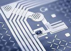
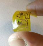
4 Application requirements Interactive, modular, flexible, large-area, OLED-based lighting system on low-cost foil with built-in intelligent light management Slide 4


5 Technology specifications = + = + PI: 20 per m2 Cu: 6 per kg PET: Al: 2.0 per m2 1.4 per kg Slide 5
 < 100 mω vias Slide 6")
6 Technology specifications Glass/Foil I 500 ma L > 3 µh R < 1 Ω 3 mm x 3 mm, 400 µm pitch 250 µm PET 50 µm Al (2x) < 100 mω vias Slide 6


7 Process flow Slide 7


8 Via drilling Via drilling by laser Aluminum is used as hard mask for CO 2 laser drilling Additional UV laser desmear after CO 2 drilling Optimize via tapering for filling process Design compensation to match foil deformation 200 µm Slide 8


9 Via drilling Desmear after CO 2 drilling Pulsed KrF laser desmear Oxigen plasma desmear Area cleaned with KrF Before plasma cleaning Deposit after CO2 drilling After plasma cleaning Slide 9


10 Via filling Via filling by stencil printing Enclosed print head (Dek ProFlow) for high-aspect ratio via filling Design of experiment on Cu-PET-Cu with CE 3103 WLV Minimize entrapped air bubbles Improve contact between ICA and copper Results Single print stroke with medium speed High ProFlow head pressure Transfer / Driving forces are influenced by:- Squeegee angle Print speed Paste rheology Paste roll volume Transfer Force Squeegee Driving Force ProFlow Slide 10
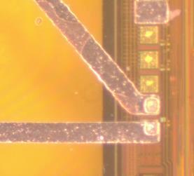
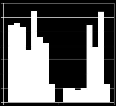
11 Via filling Via filling by stencil printing Histogram of via resistance (Ω) for 135 vias (9 samples over two printing runs) with an aspect ratio of 4:5 (350 µm depth and 450 µm diameter) > 95 % of vias are below the 100 mω target Slide 11

")
")

12 Chip mounting Flip-chip mounting using stencil printed ICA bumps Two test chips IZM28 (2.5 mm x 2.5 mm, 300 µm pitch, 20 contacts) IZM41 (0.9 mm x 0.9 mm, 500 µm pitch, 4 contacts) Bonding parameters: C and 0.5 N pressure Small contact pads on IZM28 incompatible with ICA printing Slide 12
13 Chip mounting Flip-chip mounting using stencil printed ICA bumps Low and reproducible resistance on PET-Cu Large variation in contact resistance on PET-Al C er ma O A B A B A B A B WCA -34 P 1 62,2 67,4 61,5 61,8 71,5 59,7 67,4 59,2 P 10 62,2 67,4 61,5 61,8 71,5 59,7 67,5 59,2 WCA -34 E 1 57,5 63,9 61,1 55,9 57,5 60,2 61,1 58,5 R 10 57,5 63,9 61,1 55,9 57,5 60,2 61,1 58, A inium A B A B A B A B L WCA , ,5 672,1 110, U , ,6 675, M WCA ,7 332,9 145,5 503,4 808,1 782,3 I ,4 330,8 144,9 499,6 807,6 782,4 N WCA ,9 784, ,3 238,9 799,6 306,2 464,5 I ,3 791, ,6 802,6 307,3 465,1 U WCA , , , M , ,4 611,7 91, Slide 13


14 OLED mounting Structural film adhesive combined with printed ICA bumps Very high bumps required to bridge glass encapsulation Even distribution of OLED contacts for optical uniformity Pre-structured film adhesive applied to backplane before printing Dek PumpPrint technology for printing >1.5 mm high bumps Optimized stencil design and print process make it possible to reliably print pyramidal dots with a 1:2 aspect ratio Higher aspect ratios are possible with optimized material Slide 14

 on cathode and anode sides Customized design for IMOLA applications")
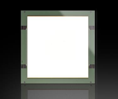
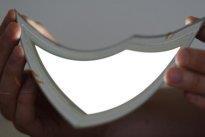
15 Increased flexibility - OLEDs Flexible OLED technology (Holst Centre) Bottom emission type, fabricated on PEN foil Efficiency of up to 47 lumens per watt (white light) SiN-OCP-SiN barrier stacks (Holst Centre IP) on cathode and anode sides Customized design for IMOLA applications Slide 15


16 Increased flexibility - OLEDs Flexible OLED technology (Holst Centre) Honeycomb shunt lines for uniform current distribution over large area (> 10 cm x 10 cm) Slide 16


17 Increased flexibility - UTCP Once the backplane is flexible. flexibility is limited by the rigid components A solution : - Thin down chips, down to foil-thickness (± 30 µm, by grinding) Die thinning < 30um - Make a flexible interposer (e.g. based on polyimide) Si die - Embeddable in or on the flexible backplane Polyimide 2 Polyimide 1 Slide 17

")


18 Increased flexibility - UTCP UTCP Si die - Small I/O pitch (< 100mm) mm thickness - PCB I/O pitch (~ 500mm) - Flexible Si die Polyimide 2 Polyimide 1 Slide 18 - UTCP interposer - Flexible - Known-Good-Package mm thickness


19 Increased flexibility - UTCP 10 mm Slide 19


20 Conclusion Al etching Ferrite printing Via filling Adhesive selection OLED mounting Chip mounting Slide 20
Active and passive component embedding into low-cost plastic substrates aimed at smart system applications
 Active and passive component embedding into low-cost plastic substrates aimed at smart system applications Maarten Cauwe 1, Bjorn Vandecasteele 1, Johan De Baets 1, Jeroen van den Brand 2, Roel Kusters
Innovative pcb solutions used in medical and other devices Made in Switzerland
 Innovative pcb solutions used in medical and other devices Made in Switzerland Chocolate Watches Money.PCB`s innovative pcb`s... Customer = innovation driver Need to add more parts and I/O make smaller/thinner
Processes for Flexible Electronic Systems
 Processes for Flexible Electronic Systems Michael Feil Fraunhofer Institut feil@izm-m.fraunhofer.de Outline Introduction Single sheet versus reel-to-reel (R2R) Substrate materials R2R printing processes
FLEXIBLE AND STRETCHABLE CIRCUIT TECHNOLOGIES FOR SPACE APPLICATIONS
 FLEXIBLE AND STRETCHABLE CIRCUIT TECHNOLOGIES FOR SPACE APPLICATIONS EMPPS WORKSHOP, NOORDWIJK, THE NETHERLANDS 20-22 MAY 2014 Maarten Cauwe, Frederick Bossuyt, Johan De Baets, Jan Vanfleteren Centre for
Design of an Integrated OLED Driver for a Modular Large-Area Lighting System
 Design of an Integrated OLED Driver for a Modular Large-Area Lighting System JAN DOUTRELOIGNE, ANN MONTÉ, JINDRICH WINDELS Center for Microsystems Technology (CMST) Ghent University IMEC Technologiepark
Modeling, Design, and Demonstration of 2.5D Glass Interposers for 16-Channel 28 Gbps Signaling Applications
 Modeling, Design, and Demonstration of 2.5D Glass Interposers for 16-Channel 28 Gbps Signaling Applications Brett Sawyer, Bruce C. Chou, Saumya Gandhi, Jack Mateosky, Venky Sundaram, and Rao Tummala 3D
Optical Bus for Intra and Inter-chip Optical Interconnects
 Optical Bus for Intra and Inter-chip Optical Interconnects Xiaolong Wang Omega Optics Inc., Austin, TX Ray T. Chen University of Texas at Austin, Austin, TX Outline Perspective of Optical Backplane Bus
Thin Film Resistor Integration into Flex-Boards
 Thin Film Resistor Integration into Flex-Boards 7 rd International Workshop Flexible Electronic Systems November 29, 2006, Munich by Dr. Hans Burkard Hightec H MC AG, Lenzburg, Switzerland 1 Content HiCoFlex:
EMERGING SUBSTRATE TECHNOLOGIES FOR PACKAGING
 EMERGING SUBSTRATE TECHNOLOGIES FOR PACKAGING Henry H. Utsunomiya Interconnection Technologies, Inc. Suwa City, Nagano Prefecture, Japan henryutsunomiya@mac.com ABSTRACT This presentation will outline
Hermetic Packaging Solutions using Borosilicate Glass Thin Films. Lithoglas Hermetic Packaging Solutions using Borosilicate Glass Thin Films
 Hermetic Packaging Solutions using Borosilicate Glass Thin Films 1 Company Profile Company founded in 2006 ISO 9001:2008 qualified since 2011 Headquarters and Production in Dresden, Germany Production
NEW PACKAGING AND INTERCONNECT TECHNOLOGIES FOR ULTRA THIN CHIPS
 NEW PACKAGING AND INTERCONNECT TECHNOLOGIES FOR ULTRA THIN CHIPS Christine Kallmayer and Rolf Aschenbrenner Fraunhofer IZM Berlin, Germany kallmayer@izm.fhg.de Julian Haberland and Herbert Reichl Technical
Advanced High-Density Interconnection Technology
 Advanced High-Density Interconnection Technology Osamu Nakao 1 This report introduces Fujikura s all-polyimide IVH (interstitial Via Hole)-multi-layer circuit boards and device-embedding technology. Employing
Chapter 11 Testing, Assembly, and Packaging
 Chapter 11 Testing, Assembly, and Packaging Professor Paul K. Chu Testing The finished wafer is put on a holder and aligned for testing under a microscope Each chip on the wafer is inspected by a multiple-point
Flexible glass substrates for roll-to-roll manufacturing
 Science & Technology Flexible glass substrates for roll-to-roll manufacturing Corning - S. Garner, G. Merz, J. Tosch, C. Chang, D. Marshall, X. Li, J. Matusick, J. Lin, C. Kuo, S. Lewis, C. Kang ITRI -
Stencil Technology. Agenda: Laser Technology Stencil Materials Processes Post Process
 Stencil Technology Agenda: Laser Technology Stencil Materials Processes Post Process Laser s YAG LASER Conventional Laser Pulses Laser beam diameter is 2.3mil Ridges in the inside walls of the apertures
Development of gating foils to inhibit ion feedback using FPC production techniques
 Development of gating foils to inhibit ion feedback using FPC production techniques Daisuke Arai (Fujikura Ltd.) Katsumasa Ikematsu (Saga Uni.), Akira Sugiyama (Saga Uni.) Masahiro Iwamura, Akira Koto,
Bumping of Silicon Wafers using Enclosed Printhead
 Bumping of Silicon Wafers using Enclosed Printhead By James H. Adriance Universal Instruments Corp. SMT Laboratory By Mark A. Whitmore DEK Screen Printers Advanced Technologies Introduction The technology
Flip Chip Bonding Using Sony Anisotropic Conductive Film (ACF) FP1526Y
 FP1526Y") Flip Chip Bonding Using Sony Anisotropic Conductive Film (ACF) FP1526Y Purpose: Author: Rekha S. Pai (07/29/03) To use ACF as an interconnection method for attaching dice to substrates. Direct electrical
Flip Chip Bonding Using Sony Anisotropic Conductive Film (ACF) FP1526Y Purpose: Author: Rekha S. Pai (07/29/03) To use ACF as an interconnection method for attaching dice to substrates. Direct electrical
PANEL LEVEL PACKAGING A MANUFACTURING SOLUTION FOR COST-EFFECTIVE SYSTEMS
 PANEL LEVEL PACKAGING A MANUFACTURING SOLUTION FOR COST-EFFECTIVE SYSTEMS R. Aschenbrenner, K.-F. Becker, T. Braun, and A. Ostmann Fraunhofer Institute for Reliability and Microintegration Berlin, Germany
Multilayer Foil Metallization for All Back Contact Cells
 Multilayer Foil Metallization for All Back Contact Cells David Levy, Natcore Technology David Carlson, CarlsonPV 44 th IEEE-PVSC Conference (June 30, 2017) 1 Overview Multilayer foil metallization Benefits
Application Bulletin 240
 Application Bulletin 240 Design Consideration CUSTOM CAPABILITIES Standard PC board fabrication flexibility allows for various component orientations, mounting features, and interconnect schemes. The starting
Technology Flexible Printed Circuits Rev For latest information please visit
 Options and Characteristics Online calculation On explicit enquiry Quantity 1 pieces up to 1m² total area 1piece to mass production Number of layers 1 to 2 layers up to 6 layers Material thickness 0,05mm
Sectional Design Standard for High Density Interconnect (HDI) Printed Boards
 Printed Boards") IPC-2226 ASSOCIATION CONNECTING ELECTRONICS INDUSTRIES Sectional Design Standard for High Density Interconnect (HDI) Printed Boards Developed by the HDI Design Subcommittee (D-41) of the HDI Committee
IPC-2226 ASSOCIATION CONNECTING ELECTRONICS INDUSTRIES Sectional Design Standard for High Density Interconnect (HDI) Printed Boards Developed by the HDI Design Subcommittee (D-41) of the HDI Committee
450mm and Moore s Law Advanced Packaging Challenges and the Impact of 3D
 450mm and Moore s Law Advanced Packaging Challenges and the Impact of 3D Doug Anberg VP, Technical Marketing Ultratech SOKUDO Lithography Breakfast Forum July 10, 2013 Agenda Next Generation Technology
FBTI Flexible Bumped Tape Interposer
 FBTI Flexible Bumped Tape Interposer Development of FBTI (Flexible Bumped Tape Interposer) * * * * *2 Kazuhito Hikasa Toshiaki Amano Toshiya Hikami Kenichi Sugahara Naoyuki Toyoda CSPChip Size Package
450mm patterning out of darkness Backend Process Exposure Tool SOKUDO Lithography Breakfast Forum July 10, 2013 Doug Shelton Canon USA Inc.
 450mm patterning out of darkness Backend Process Exposure Tool SOKUDO Lithography Breakfast Forum 2013 July 10, 2013 Doug Shelton Canon USA Inc. Introduction Half Pitch [nm] 2013 2014 2015 2016 2017 2018
Electroless Bumping for 300mm Wafers
 Electroless Bumping for 300mm Wafers T. Oppert Internepcon 2006 Tokyo Big Sight, Japan Outline Short Company Profile Electroless Ni/Au Under Bump Metallization UBM for Copper Devices Solder Bumping: Stencil
SOLDER BUMP FLIP CHIP BONDING FOR PIXEL DETECTOR HYBRIDIZATION
 SOLDER BUMP FLIP CHIP BONDING FOR PIXEL DETECTOR HYBRIDIZATION Jorma Salmi and Jaakko Salonen VTT Information Technology Microelectronics P.O. Box 1208 FIN-02044 VTT, Finland (visiting: Micronova, Tietotie
A Low-cost Through Via Interconnection for ISM WLP
 A Low-cost Through Via Interconnection for ISM WLP Jingli Yuan, Won-Kyu Jeung, Chang-Hyun Lim, Seung-Wook Park, Young-Do Kweon, Sung Yi To cite this version: Jingli Yuan, Won-Kyu Jeung, Chang-Hyun Lim,
64 Channel Flip-Chip Mounted Selectively Oxidized GaAs VCSEL Array
 64 Channel Flip-Chip Mounted Selectively Oxidized GaAs VCSEL Array 69 64 Channel Flip-Chip Mounted Selectively Oxidized GaAs VCSEL Array Roland Jäger and Christian Jung We have designed and fabricated
Assembly/Packagng RF-PCB. Thick Film. Thin Film. Screening/Test. Design Manual
 Thick Film Thin Film RF-PCB Assembly/Packagng Screening/Test Design Manual RHe Design Manual The following rules are effective for the draft of circuit boards and hybrid assemblies. The instructions are
OB-FPC: FLEXIBLE PRINTED CIRCUITS FOR THE ALICE TRACKER
 OB-FPC: FLEXIBLE PRINTED CIRCUITS FOR THE ALICE TRACKER Main Requirements. The OB FPC must meet demanding requirements: Material: Low material budget Electrical: impedance of differential lines @ 100W,
Stencil Design Considerations to Improve Drop Test Performance
 Design Considerations to Improve Drop Test Performance Jeff Schake DEK USA, inc. Rolling Meadows, IL Brian Roggeman Universal Instruments Corp. Conklin, NY Abstract Future handheld electronic products
CHAPTER 11: Testing, Assembly, and Packaging
 Chapter 11 1 CHAPTER 11: Testing, Assembly, and Packaging The previous chapters focus on the fabrication of devices in silicon or the frontend technology. Hundreds of chips can be built on a single wafer,
High Reliability and High Temperature Application Solution Solder Joint Encapsulant Paste
 High Reliability and High Temperature Application Solution Solder Joint Encapsulant Paste YINCAE Advanced Materials, LLC WHITE PAPER October 2017 2017 YINCAE Advanced Materials, LLC - All Rights Reserved.
Electrical and Thermal Analysis of an OLED Module
 Electrical and Thermal Analysis of an OLED Module Jurica Kundrata and Adrijan Barić University of Zagreb Faculty of Electrical Engineering and Computing COMSOL CONFERENCE 2012. 10.-12. October 2012. Excerpt
CMP for More Than Moore
 2009 Levitronix Conference on CMP Gerfried Zwicker Fraunhofer Institute for Silicon Technology ISIT Itzehoe, Germany gerfried.zwicker@isit.fraunhofer.de Contents Moore s Law and More Than Moore Comparison:
REVISION #25, 12/12/2012
 HYPRES NIOBIUM INTEGRATED CIRCUIT FABRICATION PROCESS #03-10-45 DESIGN RULES REVISION #25, 12/12/2012 Direct all inquiries, questions, comments and suggestions concerning these design rules and/or HYPRES
Multi-Wire Drift Chambers (MWDC)
") Multi-Wire Drift Chambers (MWDC) Mitra Shabestari August 2010 Introduction The detailed procedure for construction of multi-wire drift chambers is presented in this document. Multi-Wire Proportional Counters
Multi-Wire Drift Chambers (MWDC) Mitra Shabestari August 2010 Introduction The detailed procedure for construction of multi-wire drift chambers is presented in this document. Multi-Wire Proportional Counters
BGA (Ball Grid Array)
") BGA (Ball Grid Array) National Semiconductor Application Note 1126 November 2002 Table of Contents Introduction... 2 Package Overview... 3 PBGA (PLASTIC BGA) CONSTRUCTION... 3 TE-PBGA (THERMALLY ENHANCED
BGA (Ball Grid Array) National Semiconductor Application Note 1126 November 2002 Table of Contents Introduction... 2 Package Overview... 3 PBGA (PLASTIC BGA) CONSTRUCTION... 3 TE-PBGA (THERMALLY ENHANCED
3M XYZ-Axis Electrically Conductive Adhesive Transfer Tape (ECATT) 9723
 9723") Technical Data November, 2009 M XYZ-Axis Electrically Conductive Adhesive Transfer Tape (ECATT) 972 Product Description M XYZ-Axis Electrically Conductive Adhesive Transfer Tape (ECATT) 972 is an isotropically
Technical Data November, 2009 M XYZ-Axis Electrically Conductive Adhesive Transfer Tape (ECATT) 972 Product Description M XYZ-Axis Electrically Conductive Adhesive Transfer Tape (ECATT) 972 is an isotropically
Medical Electronics Packaging Challenges/ Solutions inemi Medical Electronics Workshop May 5, Revised Page 1
 Medical Electronics Packaging Challenges/ Solutions inemi Medical Electronics Workshop May 5, 2011 Santa Clara, CA Susan Bagen Page 1 Medical Electronics Industry Gradual production growth. Healthy growth
Min Tao, Ph. D, Ashok Prabhu, Akash Agrawal, Ilyas Mohammed, Ph. D, Bel Haba, Ph. D Oct , IWLPC
 PACKAGE-ON-PACKAGE INTERCONNECT FOR FAN-OUT WAFER LEVEL PACKAGES Min Tao, Ph. D, Ashok Prabhu, Akash Agrawal, Ilyas Mohammed, Ph. D, Bel Haba, Ph. D Oct 18-20 2016, IWLPC 1 Outline Laminate to Fan-Out
An Introduction to Electronics Systems Packaging. Prof. G. V. Mahesh. Department of Electronic Systems Engineering
 An Introduction to Electronics Systems Packaging Prof. G. V. Mahesh Department of Electronic Systems Engineering India Institute of Science, Bangalore Module No. # 02 Lecture No. # 08 Wafer Packaging Packaging
RF circuit fabrication rules
 RF circuit fabrication rules Content: Single layer (ref. page 4) No vias (ref. page 4) With riveted vias (ref. pages 4,5,6) With plated vias (ref. pages 4, 5,7,8,9,10,11) Component assembly (ref. pages
An innovative plating system
 Volume 38 Issue 1 2016 @siliconsemi www.siliconsemiconductor.net Linde: On-site generated fl uorine The year that was 2015 An innovative plating system for next generation packaging technologies Imec s
B. Flip-Chip Technology
 B. Flip-Chip Technology B1. Level 1. Introduction to Flip-Chip techniques B1.1 Why flip-chip? In the development of packaging of electronics the aim is to lower cost, increase the packaging density, improve
3D IC-Package-Board Co-analysis using 3D EM Simulation for Mobile Applications
 3D IC-Package-Board Co-analysis using 3D EM Simulation for Mobile Applications Darryl Kostka, CST of America Taigon Song and Sung Kyu Lim, Georgia Institute of Technology Outline Introduction TSV Array
3D TSV Micro Cu Column Chip-to-Substrate/Chip Assmbly/Packaging Technology
 3D TSV Micro Cu Column Chip-to-Substrate/Chip Assmbly/Packaging Technology by Seung Wook Yoon, *K. T. Kang, W. K. Choi, * H. T. Lee, Andy C. B. Yong and Pandi C. Marimuthu STATS ChipPAC LTD, 5 Yishun Street
Fraunhofer IZM - ASSID
 FRAUNHOFER-INSTITUT FÜR Zuverlässigkeit und Mikrointegration IZM Fraunhofer IZM - ASSID All Silicon System Integration Dresden Heterogeneous 3D Wafer Level System Integration 3D system integration is one
New fabrication and packaging technologies for CMOS pixel sensors: closing gap between hybrid and monolithic
 New fabrication and packaging technologies for CMOS pixel sensors: closing gap between hybrid and monolithic Outline Short history of MAPS development at IPHC Results from TowerJazz CIS test sensor Ultra-thin
Technical Capabilities Non Standard Technologies. CML pcbs from just around the corner
 Technical Capabilities Non Standard Technologies PAGE 1 Capabilities Rigid Layer Count 1-12 layer (above 12 layer see HDI) 0.4-3.2 mm (> 3.2 mm on request) Finished Board Thickness Tolerance: +/-10% Core
PCB Supplier of the Best Quality, Lowest Price and Reliable Lead Time. Low Cost Prototype Standard Prototype & Production Stencil PCB Design
 The Best Quality PCB Supplier PCB Supplier of the Best Quality, Lowest Price Low Cost Prototype Standard Prototype & Production Stencil PCB Design Visit us: www. qualiecocircuits.co.nz OVERVIEW A thin
Fabricating 2.5D, 3D, 5.5D Devices
 Fabricating 2.5D, 3D, 5.5D Devices Bob Patti, CTO rpatti@tezzaron.com Tezzar on Semiconduct or 04/15/2013 1 Gen4 Dis-Integrated 3D Memory DRAM layers 42nm node 2 million vertical connections per lay per
Okamoto Machine Tool Works, LTD. June 22, th SEMATECH Symposium Japan 1
 Okamoto Machine Tool Works, LTD 1 Contents Solutions for TSV Wafer Thinning Process (Front Side Via) TSV Wafer Thinning Challenges Process Improvement (4-years Development) TSV Wafer Thinning Tool (TSV300)
Excimer laser projector for microelectronics applications
 Excimer laser projector for microelectronics applications P T Rumsby and M C Gower Exitech Ltd Hanborough Park, Long Hanborough, Oxford OX8 8LH, England ABSTRACT Fully integrated excimer laser mask macro
S3X58-M High Reliability Lead Free Solder Paste. Technical Information. Koki no-clean LEAD FREE solder paste.
 www.ko-ki.co.jp #52007 Revised on Nov.27, 2014 Koki no-clean LEAD FREE solder paste High Reliability Lead Free Solder Paste S3X58-M500-4 Technical Information O₂ Reflowed 0.5mmP QFP 0603R This product
ESCC2006 European Supply Chain Convention
 ESCC2006 European Supply Chain Convention PCB Paper 20 Laser Technology for cutting FPC s and PCB s Mark Hüske, Innovation Manager, LPKF Laser & Electronics AG, Germany Laser Technology for cutting FPCs
Manufacture and Performance of a Z-interconnect HDI Circuit Card Abstract Introduction
 Manufacture and Performance of a Z-interconnect HDI Circuit Card Michael Rowlands, Rabindra Das, John Lauffer, Voya Markovich EI (Endicott Interconnect Technologies) 1093 Clark Street, Endicott, NY 13760
Flexline - A Flexible Manufacturing Method for Wafer Level Packages (Extended Abstract)
") Flexline - A Flexible Manufacturing Method for Wafer Level Packages (Extended Abstract) by Tom Strothmann, *Damien Pricolo, **Seung Wook Yoon, **Yaojian Lin STATS ChipPAC Inc.1711 W Greentree Drive Tempe,
Flexline - A Flexible Manufacturing Method for Wafer Level Packages (Extended Abstract) by Tom Strothmann, *Damien Pricolo, **Seung Wook Yoon, **Yaojian Lin STATS ChipPAC Inc.1711 W Greentree Drive Tempe,
Zukunftstechnologie Dünnglasbasierte elektrooptische. Research Center of Microperipheric Technologies
 Zukunftstechnologie Dünnglasbasierte elektrooptische Baugruppenträger Dr. Henning Schröder Fraunhofer IZM, Berlin, Germany Today/Overview Motivation: external roadmaps High Bandwidth and Channel Density
A Technique for Improving the Yields of Fine Feature Prints
 A Technique for Improving the Yields of Fine Feature Prints Dr. Gerald Pham-Van-Diep and Frank Andres Cookson Electronics Equipment 16 Forge Park Franklin, MA 02038 Abstract A technique that enhances the
Non-Volatile Memory Based on Solid Electrolytes
 Non-Volatile Memory Based on Solid Electrolytes Michael Kozicki Chakku Gopalan Murali Balakrishnan Mira Park Maria Mitkova Center for Solid State Electronics Research Introduction The electrochemical redistribution
2.5D Platform (Examples of products produced to date are shown here to demonstrate Amkor's production capabilities)
") Wafer Finishing & Flip Chip Stacking interconnects have emerged to serve a wide range of 2.5D- & 3D- packaging applications and architectures that demand very high performance and functionality at the
Wafer Finishing & Flip Chip Stacking interconnects have emerged to serve a wide range of 2.5D- & 3D- packaging applications and architectures that demand very high performance and functionality at the
Application Note AN-1011
 AN-1011 Board Mounting Application Note for 0.800mm Pitch Devices For part numbers IRF6100, IRF6100PBF, IR130CSP, IR130CSPPBF, IR140CSP, IR140CSPPBF, IR1H40CSP, IR1H40CSPPBF By Hazel Schofield and Philip
Holst Centre Wireless Autonomous Sensor Technologies & Flexible Electronics
 February 10, 2011 Holst Centre Wireless Autonomous Sensor Technologies & Flexible Electronics Presentation overview -General overview -Research focus < 4 Holst Centre: a solid partner in research Independent,
Substrates Lost in Translation
 2004 IEEE PRESENTATION Components, Packaging & Manufacturing Technology (CPMT) Society, Santa Clara Valley Chapter www.cpmt.org/scv/ Substrates Lost in Translation R. Huemoeller Vice President, Substrate
Data Sheet _ R&D. Rev Date: 8/17
 Data Sheet _ R&D Rev Date: 8/17 Micro Bump In coming years the interconnect density for several applications such as micro display, imaging devices will approach the pitch 10um and below. Many research
9 rue Alfred Kastler - BP Nantes Cedex 3 - France Phone : +33 (0) website :
 website :") 9 rue Alfred Kastler - BP 10748-44307 Nantes Cedex 3 - France Phone : +33 (0) 240 180 916 - email : info@systemplus.fr - website : www.systemplus.fr April 2012 - Version 1 Written by: Romain FRAUX DISCLAIMER
9 rue Alfred Kastler - BP 10748-44307 Nantes Cedex 3 - France Phone : +33 (0) 240 180 916 - email : info@systemplus.fr - website : www.systemplus.fr April 2012 - Version 1 Written by: Romain FRAUX DISCLAIMER
General-purpose Foil Strain Gages KFG
 General-purpose Foil Strain Gages KFG -8 General-purpose Foil Strain Gages in KFG Series Grid width Grid length (Gage length) Base length The KFG series gages use polyimide resin for the base approx. μm
M series. Product information. Koki no-clean LEAD FREE solder paste. Contents. Lead free SOLUTIONS you can TRUST.
 www.ko-ki.co.jp Ver. 42017e.2 Prepared on Oct. 26, 2007 Koki no-clean LEAD FREE solder paste Anti-Pillow Defect Product information This Product Information contains product performance assessed strictly
RESERVOIR PRINTING IN DEEP CAVITIES
 As originally published in the SMTA Proceedings RESERVOIR PRINTING IN DEEP CAVITIES Phani Vallabhajosyula, Ph.D., William Coleman, Ph.D., Karl Pfluke Photo Stencil Golden, CO, USA phaniv@photostencil.com
Electro-optical circuit board with single-mode glass waveguide optical interconnects
 Electro-optical circuit board with single-mode glass waveguide optical interconnects Lars Brusberg 1), Marcel Neitz 2), Dominik Pernthalter 1), Daniel Weber 2), Bogdan Sirbu 1), Christian Herbst 2), Christopher
Micro-PackS, Technology Platform. Security Characterization Lab Opening
 September, 30 th 2008 Micro-PackS, Technology Platform Security Characterization Lab Opening Members : Micro-PackS in SCS cluster From Silicium to innovative & commucating device R&D structure, gathering
Through Glass Via (TGV) Technology for RF Applications
 Technology for RF Applications") Through Glass Via (TGV) Technology for RF Applications C. H. Yun 1, S. Kuramochi 2, and A. B. Shorey 3 1 Qualcomm Technologies, Inc. 5775 Morehouse Dr., San Diego, California 92121, USA Ph: +1-858-651-5449,
Through Glass Via (TGV) Technology for RF Applications C. H. Yun 1, S. Kuramochi 2, and A. B. Shorey 3 1 Qualcomm Technologies, Inc. 5775 Morehouse Dr., San Diego, California 92121, USA Ph: +1-858-651-5449,
Laminate Based Fan-Out Embedded Die Technologies: The Other Option
 Laminate Based Fan-Out Embedded Die Technologies: The Other Option Theodore (Ted) G. Tessier, Tanja Karila*, Tuomas Waris*, Mark Dhaenens and David Clark FlipChip International, LLC 3701 E University Drive
Wafer-scale 3D integration of silicon-on-insulator RF amplifiers
 Wafer-scale integration of silicon-on-insulator RF amplifiers The MIT Faculty has made this article openly available. Please share how this access benefits you. Your story matters. Citation As Published
GSP. TOYOTA s recommended solder paste for automotive electronics. Product information. LEAD FREE solder paste.
 www.ko-ki.co.jp #47012E 2011.09.27 LEAD FREE solder paste TOYOTA s recommended solder paste for automotive electronics Product information Crack-Free Residue This Product Information contains product performance
So You Want to Print to and Below.6 AAR? Jim Price Western Regional Sales Manager
 So You Want to Print to and Below.6 AAR? Jim Price Western Regional Sales Manager What is the Goal? Print to.6 and lower area aperture ratios (AAR) without the need to use exotic stencils or restricted
Integration of 3D detector systems
 Integration of 3D detector systems Piet De Moor Introduction Evolution in radiation detection/imaging: single pixel linear array 2D array increase in resolution = decrease in pitch (down to few um) = thanks
ENGAT00000 to ENGAT00010
 Wideband Fixed Attenuator Family, DIE, DC to 50 GHz ENGAT00000 / 00001 / 00002 / 00003 / 00004 / 00005 / 00006 / 00007 / 00008 / 00009 / 00010 Typical Applications ENGAT00000 to ENGAT00010 Features Space
Introduction of IMS Technology for Advanced Solder Bumping on Wafers / Laminates
 Introduction of IMS Technology for Advanced Solder Bumping on Wafers / Laminates Science & Technology IBM Research Tokyo Yasumitsu Orii, PhD Senju Metal Industry Co.,TW Deputy General Manager Lewis Huang
Two major features of this text
 Two major features of this text Since explanatory materials are systematically made based on subject examination questions, preparation
First Demonstration of Panel Glass Fan-out (GFO) Packages for High I/O Density and High Frequency Multi-Chip Integration
 Packages for High I/O Density and High Frequency Multi-Chip Integration") First Demonstration of Panel Glass Fan-out (GFO) Packages for High I/O Density and High Frequency Multi-Chip Integration Tailong Shi, Chintan Buch,Vanessa Smet, Yoichiro Sato, Lutz Parthier, Frank Wei
First Demonstration of Panel Glass Fan-out (GFO) Packages for High I/O Density and High Frequency Multi-Chip Integration Tailong Shi, Chintan Buch,Vanessa Smet, Yoichiro Sato, Lutz Parthier, Frank Wei
2016 IEEE 66th Electronic Components and Technology Conference
 2016 IEEE 66th Electronic Components and Technology Conference Next Generation Panel-Scale RDL with Ultra Small Photo Vias and Ultra-fine Embedded Trenches for Low Cost 2.5D Interposers and High Density
AN5046 Application note
 Application note Printed circuit board assembly recommendations for STMicroelectronics PowerFLAT packages Introduction The PowerFLAT package (5x6) was created to allow a larger die to fit in a standard
Yoshihiko ISOBE Hiroshi MUTO Tsuyoshi FUKADA Seiji FUJINO
 Yoshihiko ISOBE Hiroshi MUTO Tsuyoshi FUKADA Seiji FUJINO Increased performance requirements in terms of the environment, safety and comfort have recently been imposed on automobiles to ensure efficient
Tape Automated Bonding
 Tape Automated Bonding Introduction TAB evolved from the minimod project begun at General Electric in 1965, and the term Tape Automated Bonding was coined by Gerard Dehaine of Honeywell Bull in 1971. The
MLPF-WB55-01E GHz low pass filter matched to STM32WB55Cx/Rx. Datasheet. Features. Applications. Description
 Datasheet 2.4 GHz low pass filter matched to STM32WB55Cx/Rx Features Top view (pads down) Integrated impedance matching to STM32WB55Cx and STM32WB55Rx LGA footprint compatible 50 Ω nominal impedance on
Chip Assembly on MID (Molded Interconnect Device) A Path to Chip Modules with increased Functionality
 A Path to Chip Modules with increased Functionality") T e c h n o l o g y Dr. Werner Hunziker Chip Assembly on MID (Molded Interconnect Device) A Path to Chip Modules with increased Functionality The MID (Molded Interconnect Device) technology enables the
T e c h n o l o g y Dr. Werner Hunziker Chip Assembly on MID (Molded Interconnect Device) A Path to Chip Modules with increased Functionality The MID (Molded Interconnect Device) technology enables the
Active Sensors Unit assembly process for the ATLAS High Granularity Timing Device
 Active Sensors Unit assembly process for the ATLAS High Granularity Timing Device D. Lacour for LPNHE Paris group 1. Introduction: Calice Si-W calorimeter concept 2. Gluing and positioning automated device
Advances in Laser Micro-machining for Wafer Probing and Trimming
 Advances in Laser Micro-machining for Wafer Probing and Trimming M.R.H. Knowles, A.I.Bell, G. Rutterford & A. Webb Oxford Lasers June 10, 2002 Oxford Lasers June 2002 1 Introduction to Laser Micro-machining
Thinning of IC chips
 1 Thinning of IC chips Annette Teng CORWIL TECHNOLOGY CORP. 1635 McCarthy Blvd. Milpitas, CA 95135 2 CONTENT Industry Demand for thinness Method to achieve ultrathin dies Mechanical testing of ultrathin
Copyright 2008 Year IEEE. Reprinted from IEEE ECTC May 2008, Florida USA.. This material is posted here with permission of the IEEE.
 Copyright 2008 Year IEEE. Reprinted from IEEE ECTC 2008. 27-30 May 2008, Florida USA.. This material is posted here with permission of the IEEE. Such permission of the IEEE does not in any way imply IEEE
A large-area wireless power transmission sheet using printed organic. transistors and plastic MEMS switches
 Supplementary Information A large-area wireless power transmission sheet using printed organic transistors and plastic MEMS switches Tsuyoshi Sekitani 1, Makoto Takamiya 2, Yoshiaki Noguchi 1, Shintaro
CAPABILITIES Specifications Vary By Manufacturing Locations
 Revised June 2011 Toll Free: 1-800-979-4PCB (4722) www.4pcb.com sales@4pcb.com Material FR4 RoHS RF Materials CAPABILITIES Specifications Vary By Manufacturing Locations Number of Conductive Layers Standard
Low Thermal Resistance Flip-Chip Bonding of 850nm 2-D VCSEL Arrays Capable of 10 Gbit/s/ch Operation
 Low Thermal Resistance Flip-Chip Bonding of 85nm -D VCSEL Arrays Capable of 1 Gbit/s/ch Operation Hendrik Roscher In 3, our well established technology of flip-chip mounted -D 85 nm backside-emitting VCSEL
Feature-level Compensation & Control
 Feature-level Compensation & Control 2 Sensors and Control Nathan Cheung, Kameshwar Poolla, Costas Spanos Workshop 11/19/2003 3 Metrology, Control, and Integration Nathan Cheung, UCB SOI Wafers Multi wavelength
50 Micron Pitch Flip Chip Bumping Technology: Processes and Applications
 50 Micron Pitch Flip Chip Bumping Technology: Processes and Applications Alan Huffman Center for Materials and Electronic Technologies huffman@rti.org Outline RTI Identity/History Historical development
2007-Novel structures of a MEMS-based pressure sensor
 C-(No.16 font) put by office 2007-Novel structures of a MEMS-based pressure sensor Chang-Sin Park(*1), Young-Soo Choi(*1), Dong-Weon Lee (*2) and Bo-Seon Kang(*2) (1*) Department of Mechanical Engineering,