New Broadband Common-Mode Filtering Structures Embedded in Differential Coplanar Waveguides for DC to 40 GHz Signal Transmission
|
|
|
- Penelope Sims
- 5 years ago
- Views:
Transcription

1 Rose-Hulman Institute of Technology Rose-Hulman Scholar Graduate Theses - Electrical and Computer Engineering Graduate Theses New Broadband Common-Mode Filtering Structures Embedded in Differential Coplanar Waveguides for DC to 40 GHz Signal Transmission Yujie He Follow this and additional works at: Part of the Electrical and Computer Engineering Commons Recommended Citation He, Yujie, "New Broadband Common-Mode Filtering Structures Embedded in Differential Coplanar Waveguides for DC to 40 GHz Signal Transmission" (2018). Graduate Theses - Electrical and Computer Engineering This Thesis is brought to you for free and open access by the Graduate Theses at Rose-Hulman Scholar. It has been accepted for inclusion in Graduate Theses - Electrical and Computer Engineering by an authorized administrator of Rose-Hulman Scholar. For more information, please contact weir1@rose-hulman.edu.
2 New Broadband Common-Mode Filtering Structures Embedded in Differential Coplanar Waveguides for DC to 40 GHz Signal Transmission A Thesis Submitted to the Faculty of Rose-Hulman Institute of Technology by Yujie He In Partial Fulfillment of the Requirements for the Degree of Master of Science in Electrical Engineering May 2018 Yujie He
3
4 i ABSTRACT He, Yujie M.S.E.E. Rose-Hulman Institute of Technology May 2018 New Broadband Common-Mode Filtering Structures Embedded in Differential Coplanar Waveguides for DC to 40 GHz Signal Transmission Thesis Advisor: Dr. Edward Wheeler Coplanar waveguides (CPWs) provide effective transmission with low dispersion into the millimeter-wave frequencies. For high-speed signaling, differential transmission lines display an enhanced immunity to outside interference and are less likely to interfere with other signals, when compared to single-ended transmission lines. Common-mode (CM) conversion from the differential-mode (DM) signal energy can produce unintentional radiation as well as degraded board-level electromagnetic compatibility (EMC) and signal integrity SI environments. Due to the negative effects of CM signals, filtering structures are often used to suppress the propagation of these signals. The filtering structures introduced in this project all implement the same CM filter design concept. While the concept itself is not new, the physical design of the filter combined with broadside differential CPWs had not been explored at the time of writing this thesis. The CM filtering structures described herein demonstrated to offer broadband CM filtering together with effective DM transmission into millimeter-wave frequencies. Keywords: Coplanar waveguide, common-mode filtering, electromagnetic compatibility, signal and power integrity
5 ii DEDICATION To my parents. Thank you for your support, love, and understanding. I am sorry I have not gone home for two years.
6 iii ACKNOWLEDGEMENTS I would like to express my sincere gratitude to my advisor, Dr. Edward Wheeler. His knowledge, patience, guidance, and generosity made this project possible. His encouragements have also made this journey incredible for me. I would like to thank Dr. Michael Cracraft from IBM, Poughkeepsie, NY. He is the bridge connecting the academic world and the industry world. His expertise helped me overcome many obstacles during this research. My thanks also go to Dr. Jianjian Song and Dr. Scott Kirkpatrick. Their comments and questions broadened my views from various perspectives. I would like to offer my special thanks to Joe Faia. He always offered me helpful suggestions and brilliant insights. He has inspired me on many occasions. It is a delight to work with him. I would like to thank Jack Shrader, Mark Crosby, and Gary Meyer, for their patience and technical support. I am very grateful that they are always there whenever I make a mistake. I would also like to show my gratitude to Robin J Andrews and her family for treating me like a family member. Life in another country would not be this enjoyable without her family s help. Last but not the least, I would like to express my appreciation to my family for their support throughout my life.
7 iv TABLE OF CONTENTS ABSTRACT... i DEDICATION... ii ACKNOWLEDGEMENTS... iii LIST OF FIGURES... vi LIST OF TABLES... ix GLOSSARY... xii 1. INTRODUCTION COMMON-MODE FILTERING AND S-PARAMETER MEASUREMENTS Electromagnetic Waves and Transverse Electromagnetic Mode Even Mode Analysis and Odd Mode Analysis Even Mode Odd Mode Differential Mode and Common Mode S parameters and Vector Network Analyzer (VNA) Measurement Common Mode Filtering DESIGN OF THE COMMON MODE FILTERING STRUCTURE Original Design and Simulation Improved Design Single Filter Design Cascaded Filter Design Centered and Off-Centered Stub Filter Designs Simple RF Launch Design and Simulation Sensitivity and Registration Study SIMULATION RESULTS Simulation Results for Each Filter Design without RF Launch Structure Single Filter Design Cascaded Filter Design Centered and Off-Centered Stub Filter Designs Simulation Results for Each Filter Design with RF Launch Structure... 42
8 v Single Filter Design Cascaded Filter Design Off-center Stub Filter Design Refinement of the RF Launch Design MEASUREMENT ANALYSIS Test Setup Equipment Setup Calibration De-embedding Signal Launch Effects of the Structure Measurement Results and Analysis Measurement Challenges Single Filter Design at 16 GHz with 10 GHz 10-dB Bandwidth Cascaded Filter Design at 8, 11, and 16 GHz with Multi-GHz 10-dB Bandwidths Centered and Off-centered Reference Stub Filter Design at 16 and 32 GHz with Multi-GHz 10-dB Bandwidths Minimum Impact on DM and CM Transmissions with Different Trace to Reference Spacings Minimum Impact on DM and CM Transmissions with Different Filter to Filter Spacings CONCLUSIONS REFERENCES APPENDIX A - Final Board Layout APPENDIX B MATLAB Code Code for DM and CM Transmissions Code for Function MixedMode_CST Code for Function cplx2db Code for Function loadsnp APPENDIX C Published Paper APPENDIX D Submitted Paper... 81
9 vi LIST OF FIGURES Figure 1.1 Perspective view of (a). a single-ended signaling path; (b). a differential signaling path on a printed circuit board Figure 1.2 Cross-sections of (a). microstrip differential structure, (b). stripline differential structure, and (c). coplanar waveguide differential structure Figure 2.1 Schematic of a coupled coplanar waveguide Figure 2.2 Transversal electrical field of a coupled CPW under (a). even mode excitation; (b). odd mode excitation Figure 2.3 Simplified model of a 4-port differential signaling system Figure 2.4 Electric field of a differential CPW structure (a). under DM signals; (b). under CM signals; (c). under CM with CM filtering elements presenting; (d). under DM with CM filtering elements presenting Figure 3.1 (a). Filter layer view of the original design; (b) Simulated DM and CM transmission of the original design Figure 3.2 (a) Top view of the filter layer of the original single filter design, (b) close-up view of a single filter with all dimensions labeled Figure 3.3 Simulated DM and CM transmission of a CPW board with (a) a 10 GHz filter, and (b) a 20 GHz filter Figure 3.4 Open circuit and short circuit models of the CM filtering element Figure 3.5 (a) Top view, (b) bottom view and (c) cross-section view of the new stack-up of the PCB Figure 3.6 Filter layer view of the cascaded 8, 11 and 16 GHz filter design Figure 3.7 Filter layer view of the cascaded 16 and 32 GHz filter design with centered reference stub Figure 3.8 Filter layer view of the single filter design with off-centered reference stub Figure 3.9 (a) Top view of the originally proposed RF launch structure; (b) Port model of the proposed RF launch structure. The PEC columns represent the locations of the two ground pads and the center signal pad Figure 3.10 (a) Top view of the board design with the original RF launch attached. It is worth mentioning for this model, the filter is designed to attenuate CM signals at 8 GHz; (b) Simulation results of this structure with this proposed RF launch Figure 3.11 Simulated DM and CM transmissions of the board in Fig. 3.9 (a) without the proposed RF launch model Figure 3.12 (a) Top view of the board design with the RF launch and via fence. (b) Comparison between the simulation results of this structure with and without the proposed RF launch with via fence Figure 3.13 Thru model of the proposed RF launch model Figure 3.14 Simulated transmission and reflection results of this proposed model Figure 3.15 Simulation model, with each parameter labeled, for the two cases in sensitivity study
10 Figure 3.16 Simulated (a) DM transmission and (b) CM transmission of the structure shown in Fig in a substrate sensitivity test Figure 3.17 Cross-section model of (a) a board with substrate thickness of 0.77 mm, trace width of mm, and gap width of mm, and (b) a board with substrate thickness of mm, trace width of mm, and gap width of mm in FEMAS Figure 3.18 Simulated results of the registration study: (a). differential mode signal transmission; (b). common mode signal transmission Figure 4.1 Cross-section view of the simulated electrical flux lines of a differential CPW structure with (a). the proposed filter structure shown in Fig. 3 and 4 under CM signals; (b). the same structure under DM signals; (c). a differential CPW structure without any filter structure under CM signals; (d). the same structure under DM signals Figure 4.2 Simulated transmission results of a differential CPW structure with a 16 GHz CM filter Figure 4.3 Simulated results of a differential CPW structure with cascaded 8, 11 and 16 GHz CM filters. The olive-green dashed line signifies where all -10 db bandwidths are located Figure 4.4 Simulated differential signaling transmissions of (a) cascaded 16 GHz and 32 GHz filters with centered filter-to-reference stub and (b) single filter with off-centered filter-toreference stub achieving multi-frequency filtering Figure 4.5 Simulated transmission results of a differential CPW structure with a single 16 GHz filter with and without the proposed launch structure Figure 4.6 Simulated transmission results of a differential CPW structure with cascaded 8, 11 and 16 GHz filters with and without the proposed launch structure Figure 4.7 Simulated transmission results of a differential CPW structure with cascaded 16 GHz and 32 GHz filters with centered filter-to-reference stub with and without the proposed launch structure Figure 4.8 Simulated transmission results of a differential CPW structure with a single filter with off-centered filter-to-reference stub with and without the proposed launch structure Figure 4.9 Two different transmission line models for the RF launch study Figure 4.10 Simulated results of (a). a CPW structure with 8, 11, and 16 GHz filter with 50 mm transmission line and (b). a CPW structure with 8, 11, and 16 GHz filter with 87 mm transmission line Figure 4.11 Two different taper models for the RF launch study Figure 4.12 Simulated results of (a). a CPW structure with 8, 11, and 16 GHz filter with 1.5 mm launch taper and (b). a CPW structure with 8, 11, and 16 GHz filter with 13 mm launch taper.. 49 Figure 4.13 Close-up view of the RF launch model with long taper Figure 5.1 PCB model of the final product Figure 5.2 Manufactured PCB for testing Figure 5.3 PCB measurement test setup with a 2-port VNA. The broadband loads are on the other side of the PCD, thus not showing Figure 5.4 PCB measurement test setup with a 4-port VNA Figure 5.5 Structures used for de-embedding. No filtering element is placed in these structures Figure 5.6 Phase plots of the difference of the transmission lines shown in Fig vii
11 Figure 5.7 Calculated effective permittivity of the manufactured PCB Figure 5.8 Physically impossible DM transmission results from the untreated PCB Figure 5.9 Uneven solder surface on the signal launch pad (left), and the flat pad surface after removal (right) Figure 5.10 Measured and simulated transmission results of a differential CPW structure with a single 16 GHz filter Figure 5.11 De-embedded results and simulated transmission of a differential CPW structure with a single 16 GHz filter Figure 5.12 Measured and simulated transmission results of a differential CPW structure with the cascaded filters Figure 5.13 De-embedded results and simulated transmission of a differential CPW structure with the cascaded filters Figure 5.14 Measured and simulated transmission results for cascaded 16 GHz and 32 GHz filters with centered filter-to-reference stub Figure 5.15 Measured and simulated transmission results for cascaded 16 GHz and 32 GHz filters with off-centered filter-to-reference stub Figure 5.16 De-embedded measured and simulated results for the cascaded 16 GHz and 32 GHz filters with centered filter-to-reference stub Figure 5.17 De-embedded measured and simulated results for the cascaded 16 GHz and 32 GHz filters with off-centered filter-to-reference stub Figure 5.18 Comparison of measured results for the cascaded CM filtering structures with different transmission line to reference spacing Figure 5.19 Comparison of measured results for the cascaded CM filtering structures with different filter to filter spacing viii
12 ix LIST OF TABLES Table 3-1 Dimensions of a 16 GHz CM Filtering CPW Design Shown in Fig. 3 and Table 3-2 Dimensions of the 8 GHz and 11 GHz CM Filtering CPW Designs Table 3-3 Simulated DM and CM Impedances of the Two Structures Shown in Fig
13 x LIST OF ABBREVIATIONS CM Common Mode CPW Coplanar Waveguide DM Differential Mode EMC Electromagnetic Compatibility GCPW Grounded Coplanar Waveguide GND Ground IC Integrated Circuit MW Microwave PCB Printed Circuit Board RF Radio Frequency SI Signal Integrity
14 xi LIST OF SYMBOLS English Symbols A C C Hz V m Wb Z Ampere Coulomb Capacitance Hertz Voltage Meter Weber Impedance Greek Symbols ρ Electric charge density, in C/m 3. ω ε Frequency, in rad. Permittivity Mathematical Symbols B Magnetic flux density vector, in Wb/m 2. D Electric flux density vector, in C/m 2. E Electric field vector, in V/m. H Magnetic field vector, in A/m. J Electric current density vector, in A/m 2. M Magnetic current density vector, in V/ m 2.
15 xii GLOSSARY Common Mode Signal Common Mode Impedance Differential Signaling Differential Mode Signal Differential Mode Impedance Even Mode Impedance Odd mode Impedance The half-sum of the differential voltage pair in a differential signaling system. Impedance between the differential pair when the transmission line pair is driven by a common source. A signaling method that transmits data and information using a pair of complementary signals, each in its own transmission line. The receiving signal is also called differential mode signal. The difference of the differential voltage pair in a differential signaling system. Impedance between the differential pair when the transmission line pair is driven by a differential source. Impedance of a single-ended transmission line when the two lines in a differential pair are driven by a common source. Impedance of a single-ended transmission line when the two lines in a differential pair are driven by a differential source.
16 xiii
17 1 1. INTRODUCTION The term microwave (MW) is used for electromagnetic waves with frequencies that range from 300 MHz to 300 GHz, which correspond to wavelengths from 1 m to 1 mm in free space. Microwave technology was introduced to commercial communication after its success during World War II. Early in the history of wireless communication, it was found that microwaves cannot be reflected by the ionosphere but are capable of carrying much more information that the lower frequency signals that can be reflected [1]. Nowadays, microwaves are widely used in both wired and wireless systems, in both printed circuit boards (PCB) and integrated circuits (IC). With each new generation of semiconductor technology that brings more transistors onto chips, computing devices are becoming progressively more powerful. In order to keep up with the increasing speed of computing performance and volume of data transmission, signal communication speed has also been increasing. At lower frequency, most systems can transmit signals with sufficient fidelity over a short range. As communication systems require faster data transmission and higher signal frequencies, the transmitted signals become increasingly vulnerable to attenuation, distortion, noise, and loss. Signal integrity (SI) becomes one of the most concerned topics in the microwave frequency communication industry.
18 2 Signal integrity, as well as electromagnetic compatibility (EMC), are properties that play vital roles in communication engineering. SI represents the quality of a transmitted electrical signal, while EMC represents how well the structure can work with other structures as unintentional and unwanted generation, emission, and coupling of electromagnetic energy cause interference. At high frequencies, transmission line effects and impedance mismatch can have negative effects on SI. Ringing, reflections, and ground bounce caused by these effects can hamper the response of the transmitted signal and damage the integrity. Therefore, minimizing these effects is one of the primary goals of SI engineering, particularly with high-speed designs. On the other hand, the study of EMC pursues the prevention of the generated electromagnetic energy by the structure, since the emitted electromagnetic energy can couple to other structures, causing malfunctions and breakdowns of the neighboring designs. Traditional single-ended signaling is the simplest method to transmit signals. It utilizes two conducting wires to guide the input electric energy. One is the signal trace carrying a varying voltage to transfer data, and the other is usually tied to ground (GND) serving as the reference. The receiving circuit responds to the difference between the transmitted voltage and the reference voltage. Figure 1.1 (a) shows a single-ended signaling scheme implemented on a PCB. Radiations and electric and magnetic couplings are two major reasons causing the degradation of SI and EMC performances. Any electrically charged structure will emit electromagnetic radiation, and any charged structure will have coupling to its neighboring structure. Assuming
19 3 two single-ended wires each carry a signal, as the frequency goes up, each single-ended current will interfere with neighboring circuits due to the increasing electrical and magnetic coupling. Therefore, single-ended systems suffer from poor noise immunity at high frequencies. Differential signaling is frequently used as an alternative method to transfer data. It typically has a higher noise immunity comparing to single-ended signaling. A differential system, as illustrated in Fig 1.1 (b), consists of a pair of conductors that carries two complementary signals sent from a differential source. The transmitted and received signal of a differential system is the electrical difference between the two conducting traces that carry a pair of complementary signals, which is referred to as a differential mode (DM) signal. The benefits of using differential circuits are that they can theoretically provide much higher noise immunity than single-ended systems. The single-ended signaling and differential signaling differ in how the noise signals affect the received signal. Assuming random noises, VN, occur along both types of signaling paths. VN in the single-ended system simply add to the signal voltage and so will be received at the receiving end. On the other hand, VN in the differential signaling system is common to both traces and can be subtracted away at output. The complementary signals in a differential signaling system result in much lower radiations and couplings. Due to this inherent higher noise immunity, differential signaling is much less of a threat to its neighboring circuits and compatible with lower voltage and/or current signals which can help reduce power levels.

 is introduced through signal routing paths (e.g., any time the signal is routed around a corner resulting in one trace being electrically longer than the other).")

20 4 (a) (b) Figure 1.1 Perspective view of (a). a single-ended signaling path; (b). a differential signaling path on a printed circuit board. However, a design challenge is introduced when using differential signaling. To maintain an ideal differential communication link, both signal traces must have the same electrical lengths and coupling to reference. Unfortunately, this ideal circuit is physically impossible to fabricate. Length differences (skew) is introduced through signal routing paths (e.g., any time the signal is routed around a corner resulting in one trace being electrically longer than the other). Unequal coupling can be introduced when one trace is closer to neighboring circuits than the other (e.g., if the neighboring circuit is on the same layer of metallization, the one trace will necessarily be closer than the other, resulting in the unequal electric field or capacitive coupling). Both skew and unequal coupling in a differential signaling path can result in common-mode (CM) conversion, in which a portion of the DM signal energy is converted to form an unwanted CM signal energy. CM signals share the same magnitude and polarity. Unlike DM signals, CM signals do not carry any important data and will add together instead of canceling each other out
21 5 at the receiving end, creating unwanted noise, radiation, and attenuate signals. These CM signals are inevitable in any real circuits. Therefore, the design of CM filtering structures that can suppress the propagation of CM signals while allowing DM signals to propagate is an important part of SI engineering, especially in high-speed and high-performance systems. Three commonly used transmission line designs for differential signaling are microstrip, stripline, and coplanar waveguide (CPW) structure. A differential microstrip has two conductors on a dielectric substrate and a metallization plane on the other side of the substrate as a reference. For a symmetric stripline structure, which is more widely used than an asymmetric stripline, two conductors are placed in a dielectric with two reference layers placed applied above and below the substrate. The differential transmission line using broadside coupled CPWs consists of two sides, each with a center conducting wire separating two traces acting as a reference. Crosssections of these three structures are shown in Fig 1.2.
 or")
![composite right-/left-handed (CRLH) filtering structures in microstrip transmission lines [2]-[4].](/docs-images/86/94891249/images/22-1.jpg "On the other hand, previous works have demonstrated the potential of CPW structures for high-speed signal systems.")
22 6 Figure 1.2 Cross-sections of (a). microstrip differential structure, (b). stripline differential structure, and (c). coplanar waveguide differential structure. Although not much work has been done in CM filtering for CPW differential signaling, many research reports have shown the effective CM filtering using complementary split ring resonator (CSRR) or composite right-/left-handed (CRLH) filtering structures in microstrip transmission lines [2]-[4]. On the other hand, previous works have demonstrated the potential of CPW structures for high-speed signal systems. [5] and [6] show effective characteristics of single-ended CPW transmission lines from DC up to 0.5 THz. When this project first started exploring the possibility of CM filtering using CPW structures (as discussed in section 4.1), simulated DM transmission result seemed too perfect and ideal due to not many related works being found. The publication of [5] and [6] encourages us to keep investigating the potential of CM filtering in CPW transmission lines.
23 7 This thesis investigates a unique filtering structure employed in CPW differential signaling structures. Simulations and measurements of bowtie or dipole-like filtering elements are investigated as candidate structures which can be implemented in multilayer PCBs to suppress CM transmission while allowing the propagation of DM signals. It has potential application in highspeed data transmission systems such as cellular systems and computer expansion buses as a means of protecting a PCB s SI performance while enhancing its EMC properties.
24 8 2. COMMON-MODE FILTERING AND S-PARAMETER MEASUREMENTS To understand the proposed CM filtering concept, we need to know how to analyze the differential CPW structure and how the wave travels in it. In addition to that, we also need to understand what parameter and measuring technique can help us verify our simulated and fabricated model. For a differential CPW structure, true transverse electromagnetic mode does not exist. To find the best location to place our filtering elements, we will need the help of even and odd mode, and differential and common mode analyses. As for measurement, scattering parameters are used to measure the power waves being transmitted and reflected at each port of the device. In the following section, we will explain each term to help readers understand how we came up with our filtering designs. 2.1 Electromagnetic Waves and Transverse Electromagnetic Mode Electromagnetic energy transmits in the form of waves. The directions of electric and magnetic fields of wave transmission can have different orientations to the direction of the traveling wave, depending on the propagation mode. It s possible that many field configurations exist for a given electromagnetic boundary value problem. A transverse electromagnetic mode (TEM mode) is one of these configurations whose both electric and magnetic fields are restricted to directions perpendicular (transverse) to the wave s propagation direction.
25 9 Maxwell s equations are needed to demonstrate TEM mode. Maxwell s equations are a set of four differential equations that describe how electric and magnetic fields propagate and interact. The general form of Maxwell s equations can be written as: E = jωμh, (Equation 2-1) H = jωεe, (Equation 2-2) D = ρ, (Equation 2-3) B = 0. (Equation 2-4) The script quantities are defined below: E is the electric field vector, in V/m. H is the magnetic field vector, in A/m. B is the magnetic flux density vector, in Wb/m 2. D is the electric flux density vector, in C/m 2. M is the magnetic current density vector, in V/ m 2. J is the electric current density vector, in A/m 2. ρ is the electric charge density, in C/m 3. ω is the frequency, in rad. It is worth mentioning that magnetic current is often used for mathematical convenience and completeness since magnetic charge or the magnetic monopole is not known to exist. A loop of electric current or a magnetic dipole is the true source of magnetic current. Assuming the wave is
26 10 a uniform plane wave traveling in the a z direction, the electric filed and magnetic field have only x and y components, respectively. Differential transmission lines, for example, striplines, are usually able to support TEM waves since they consist of two conductors in a homogeneous dielectric and have zero longitudinal field components. But transmission lines in CPW structures without cover plates, as seen in Fig 1.2 (c), are surrounded by more than one medium. A portion of the signal waves can transmit in free space. Consequently, a very small longitudinal component can be found, and true TEM mode does not present. This approximation of TEM mode is called quasi-tem mode. Because of this, the effective permittivity of the dielectric can be different than the labeled material permittivity. 2.2 Even Mode Analysis and Odd Mode Analysis Most differential signaling designs in microwave engineering involve symmetric transmission lines. When two transmission lines are placed closely, their fields and power can be coupled from one conductor to the other. The amount of coupling usually depends on the distance between transmission lines and signal frequencies. Figure 2.1 shows a broadside coupled coplanar waveguide, whose cross-section also appeared in Fig 1.2 (c). Using superposition, any arbitrary excitation of this CPW structure can be considered as a combination of two modes: even and odd. Both excitation modes are illustrated in Fig 2.2, where the red lines represent electric flux.
.")


27 11 Figure 2.1 Schematic of a coupled coplanar waveguide Figure 2.2 Transversal electrical field of a coupled CPW under (a). even mode excitation; (b). odd mode excitation Even Mode For even mode analysis, a magnetic wall is placed along the plane of symmetry to restrict the analysis to either the top or bottom half of the structure. The total capacitance then is expressed as C e, where the capacitance per unit length is contributed by half of the substrate, h 1. C e can be calculated using
28 12 K(k C e = 2ε 0 ε e ) r, (Equation 2-5) K(k e ) and k e = sinh( πw 4h1 ) sinh( π(w+2s) ) 4h1, (Equation 2-6) where W is the width of the conductor and S is the gap between the conductor and GND reference trace. K(k e ) and K(k e ) are the complete elliptic integral of the first kind and its complement [8]. The effective dielectric constant for even mode is defined using Ce and the even mode capacitance per unit length with air as the dielectric can be expressed as: K(k C e air = 2ε e ) 0, (Equation 2-7) K(k e ) ε eff even = C e C e air. (Equation 2-8) Hence, the even mode characteristic impedance Z 0,e can be expressed as: Z 0,e = 1 c C e C e air, (Equation 2-9) where c is the speed of light in free space [8] Odd Mode Similar to even mode analysis, an electric wall is placed along the plane of symmetry for odd mode analysis to simplify calculation to either top or bottom half of the structure. The total capacitance then is expressed as C o, where the capacitance per unit length is contributed by half of the substrate, h1. K(k C o = 2ε 0 ε o ) r, (Equation 2-10) K(k o )
29 13 and k o = tanh( πw 4h1 ) tanh( π(w+2s) ) 4h1, (Equation 2-11) where W is the width of the conductor and S is the gap between the conductor and GND reference trace. K(k o ) and K(k o ) are the complete elliptic integral of the first kind and its complement [8]. The effective dielectric constant for even mode is defined using Ce and the odd mode capacitance per unit length with air as dielectric: K(k C o air = 2ε o ) 0, (Equation 2-12) K(k o ) ε eff odd = C o C o air. (Equation 2-13) The odd mode characteristic impedance Z 0,o can be expressed as Z 0,o = 1 c C o C o air. (Equation 2-14) where c is the speed of light in free space [8]. as The characteristic impedance, Z c or Z 0, of a single-ended transmission line can be expressed Z c = Z 0 = Z 0,o Z 0,e (Equation 2-15) Differential Mode and Common Mode As seen in Fig 2.1, V1 and V2 is the differential voltage pair sent to the transmission lines. Using even mode voltage V e and odd mode voltage V o, V 1 and V 2 are defined as V 1 = V e + e γ ez + V e e γ ez + V o + e γ oz + V o e γ oz, (Equation 2-16)
30 14 since V e = V 1+V 2 2 V 2 = V e + e γ ez + V e e γ ez V o + e γ oz V o e γ oz, (Equation 2-17) and V o = V 1 V 2 2. Therefore, the resulting currents i 1 and i 2 are: i 1 = 1 (V + Z e e γez V e e γez ) + 1 (V + 0,e Z o e γoz V o e γoz ), (Equation 2-18) 0,o i 2 = 1 (V + Z e e γez V e e γez ) + 1 ( V + 0,e Z o e γoz + V o e γoz ). (Equation 2-19) 0,o Define differential mode (V d ) and common mode (V c ) voltages and currents (i d and i c ) as: Substitute V 1 and V 2, i 1 and i 2 : V d = V 1 V 2, (Equation 2-20) V c = V 1+ V 2 2 i d = i 1+ i 2 2, (Equation 2-21), (Equation 2-22) i c = i 1 + i 2. (Equation 2-23) V d = 2(V o + e γ ez + V o e γ oz ), (Equation 2-24) V c = V e + e γ ez + V e e γ ez, (Equation 2-25) i d = V o + e γ ez V o e γ oz Z 0,o, (Equation 2-26) i c = 2(V e + e γ ez V e e γ ez ) Z 0,e. (Equation 2-27) When only considering the positive differential voltages and currents, the differential mode characteristic impedance Z d and common mode characteristic impedance Z c for a symmetric CPW differential signaling system in Fig 2.1 can be expressed as: Z d = V d + i d + = 2Z 0,o, (Equation 2-28)

31 15 Z c = V c + i c + = Z 0,e 2. (Equation 2-29) 2.3 S parameters and Vector Network Analyzer (VNA) Measurement A simplified model of a coupled differential signaling system is shown in Fig 2.3, assuming port 1 and 3 are the system inputs, and port 2 and 4 are the outputs. Under perfect circumstances, all signals incident in port 1 should transmit to port 2, and none should be received at port 4. The same applies to signals sent from port 3. Figure 2.3 Simplified model of a 4-port differential signaling system. In microwave and millimeter-wave engineering, various parameters are used to describe electrical behaviors of linear electrical networks. Parameters like admittance parameters (Y parameters) and impedance parameters (Z parameters) are useful in many circumstances. Direct measurements of these parameters are difficult since equipment that can measure voltage and current at MW frequencies is simply not available. Thus, scattering parameters (S parameters) are required to characterize system performance at high frequencies. The magnitude of S parameters are ratios of power waves which are proportional to the square root of a wave s power being transmitted and reflected. Therefore, they do not require open or short circuit
32 16 conditions like Y and Z parameters. Instead, matched loads (reference impedance) are used to characterize linear electrical networks. Each port combination in a linear network has its own associated S parameter, which is defined in terms of incident and reflected powers. The quantity a n is used to represent a wave incident to port n and b n is used to represent a wave reflected from port n. For the 4-port network that s illustrated in Fig 2.3, the single-ended S parameter matrix is: S 11 S 12 S 13 S 14 S ( 21 S 22 S 23 S 24 ), S 31 S 32 S 33 S 34 S 41 S 42 S 43 S 44 where b 1 b 2 b 3 a 1 a 2 S 11 S 12 S 13 S 14 S ( ) = ( 21 S 22 S 23 S 24 ) ( S 31 S 32 S 33 S 34 a ). (Equation 2-30) 3 b 4 S 41 S 42 S 43 S 44 a 4 Due to it being passive and reciprocal, the network s S parameter is equal to its transpose, which means S mn = S nm. S 11 and S 33 are the forward reflection coefficients, when S 22 and S 44 are the reverse reflection coefficients. S 21 and S 43 are the forward gains with a source (usually 50 Ω in practice) and matching loads, and S 12 and S 34 are the reverse gains of the network under the same condition. For an ideal transmission line, magnitudes of S 11, S 33, S 22, and S 44 should equal to 0, representing zero reflection, and the magnitudes of S 21 and S 43 should be 1, representing zero loss.
33 17 In addition to the 4-port single-ended S parameter matrix, a mixed mode S parameter matrix is used to characterize the network in terms of differential and common mode signals: b d1 b d2 b c1 a d1 a d2 S dd11 S dd12 S dc11 S dc14 S ( ) = ( dd21 S dd22 S dc21 S dc24 ) ( S cd11 S cd12 S cc11 S cc34 a ). (Equation 2-31) c1 b c2 S cd21 S cd22 S cc21 S cc44 a c2 S dd21 is the input differential insertion loss. S cc21 is the common mode rejection. S cd21 is the differential to common mode conversion from port 1 to port 2. To limit CM transmission and conversion, S cc21 and S cd21 should be minimal. To calculate S dd21 and S cc21 from VNA measurements, S dd21 and S cc21 can be rewritten as: S dd21 = 0.5 (S 21 S 23 S 41 + S 43 ), (Equation 2-32) S cc21 = 0.5 (S 21 + S 23 + S 41 + S 43 ), (Equation 2-33) S cd21 = 0.5 (S 21 S 23 + S 41 S 43 ). (Equation 2-34) In addition, the forward differential return loss (port 1 reflection) S dd11 and reverse differential return loss (port 2 reflection) S dd22 can be rewritten as: S dd11 = 0.5 (S 11 S 13 S 31 + S 33 ), (Equation 2-35) S dd22 = 0.5 (S 22 S 24 S 42 + S 44 ). (Equation 2-36) For ideal transmission, they should also be kept minimal.

34 Common Mode Filtering To effectively eliminate common mode noise, the filter structure should affect either the CM electric or magnetic field between the transmission line conductors. In this thesis, a metallization plane that is tied to the reference is placed in the horizontal plane of symmetry to act as an electric wall and achieve effective CM filtering results. Illustrations of the electric flux for a differential CPW under DM and CM are shown below in Fig 2.4 (a) and (b), respectively. Figure 2.4 (c) and (d) demonstrate how a GND conductor plane in the substrate can affect CM signals but not DM signals. Figure 2.4 Electric field of a differential CPW structure (a). under DM signals; (b). under CM signals; (c). under CM with CM filtering elements presenting; (d). under DM with CM filtering elements presenting.
, consists of only simple rectangular cutouts in the middle metallization plane. The metal in the simulated model is lossy copper with 0.035mm thickness, and the dielectric is MEGTRON 6.")
35 19 3. DESIGN OF THE COMMON MODE FILTERING STRUCTURE 3.1 Original Design and Simulation The original CPW CM filter design, as shown in Fig 3.1 (a), consists of only simple rectangular cutouts in the middle metallization plane. The metal in the simulated model is lossy copper with 0.035mm thickness, and the dielectric is MEGTRON 6. The simulation results, as seen in Fig. 3.1 (b), show outstanding DM transmission and CM filtering up to 100 GHz, where S2(1),1(1) represent the DM transmission and S2(2),1(2) represent the CM transmission. The original design model and simulated data were lost due to an unfortunate hacking. Therefore, we are unable to show the exact dimensions of the simulated model. (a) (b) Figure 3.1 (a). Filter layer view of the original design; (b) Simulated DM and CM transmission of the original design.

36 Improved Design Single Filter Design I. Filter Design Concept The improved CPW CM filter design uses the same stack up as the design shown in the previous section. As before, it acts as a half-wavelength resonator but consists of a rectangular metal patch placed in the middle metallization layer, as shown in Fig. 3.2 (a), with two stubs connecting the structure to the surrounding reference plane. Figure 3.2 (b) shows the details of this proposed design with all parameters labeled, where fl is the filter length, fw is the filter width, sl is the stub length and sw is the stub width. With every dimension of the filter parameterized, the relationship between the physical structure of a filter and its effective length in a differential CPW environment can be readily explored. (a) (b) Figure 3.2 (a) Top view of the filter layer of the original single filter design, (b) close-up view of a single filter with all dimensions labeled.
37 21 II. Filter Effective Length The physical length of a filter in a PCB is not typically its effective filter length due to parasitic elements and/or fringing capacitance. Because of this, finding the effective length is important for our filter design. A correct approximation can help engineers design the filter to target CM signals at the required frequency correctly. To help us obtain a better understanding of the filtering behavior of this half-wavelength resonator design, we modeled two filters that are aimed at 10 GHz (λ/2 = 8.8 mm) and 20 GHz (λ/2 = 4.4 mm), respectively, for two models. From the simulation results shown in Fig. 3.3, it is clear that the simulated CM filtering frequencies are lower than what we initially designed for, even though the -10 db filtering bandwidth covers the targeted frequency for each case. The simulated filtering frequency for the 10 GHz filter is GHz, and the simulated filtering frequency for the 20 GHz filter turns out to be GHz. (a)
38 22 (b) Figure 3.3 Simulated DM and CM transmission of a CPW board with (a) a 10 GHz filter, and (b) a 20 GHz filter. The first approach we take to find the effective length is inspired by the microstrip model introduced by E.O Hammerstad and F. Bekkadal [7]. The length extension, l, of a microstrip line can be approximated with l = 0.412d ( ε eff+0.3 ε eff ) (w+0.262d w+0.813d ), where d is substrate thickness, w is the transmission line width, and ε eff is the effective permittivity. The extended length is physically due to fringing flux which does not immediately go to zero at the end of the conductor. Even when the filtering element is essentially a stripline structure, this equation can be employed to obtain a first estimate of the length extension of a filter. The calculated length extension is around mm for each filter. Unfortunately, applying this answer did not give us satisfying results as the expected filtering frequencies are


39 23 calculated to be GHz and GHz instead of the GHz and GHz we have from the simulation. The second approach taken is to use the open circuit and short circuit models of a CPW structure. This method is inspired by the design rule mentioned in R.N. Simons work [8]. The filter structure can be seen as either an open circuit model or a short circuit model, depending on the location of the observation as demonstrated in Fig Figure 3.4 Open circuit and short circuit models of the CM filtering element. The length extension, Δl open, of an open circuit model can be expressed as Δl open = C open C W + 2S 4 Since the gap, g, is usually much larger than W + 2S for the filter design, and the length extension, Δl short, of a short circuit model can be expressed as
40 24 Δl short = L open L W + 2s 8 In both assumptions, length extensions are considered as frequency independent since the effective permittivity of the dielectric is fairly consistent over a wide range of frequencies. Therefore, we can find Δl open = mm and Δl short = mm with the help of these equations. The filtering frequencies are expected to be GHz for the 10 GHz filter and GHz for the 20 GHz filter with the length extension of an open circuit, adding the short circuit length extension to the 10 GHz and 20 GHz filters moves the expected filtering frequencies to GHz and GHz. All results are far from the simulated CM filtering frequencies. The length extensions due to fringing are much smaller than the physical lengths of the filter, and so would result in only minor adjustments in any case. After several unsuccessful attempts at estimating the effective half-wavelength resonator length, another effective length model is suggested. The assumed effective length of a filter, leff, includes the stub length and half of the width of the metal patch so that the half-wavelength of the target frequency would be estimated using l eff = 2( fl 2 + fw 2 + sw), where resonances are expected to occur at l eff = n λ 2, where n = 1, 3. Since the filter width fw is mm and the stub width sw is mm, the approximated effective filter length is mm for the 10 GHz filter and mm for the 20 GHz filter, which gives expected filtering frequencies at GHz and GHz, respectively. Both answers are very close to the simulated GHz and GHz in Fig. 3.3.
41 25 To validate this effective length approximation, we built two additional CPW models with different CM filtering structures. One has an 8 GHz filter that actually filters at 7.5 GHz in simulation, and the other has a 35 GHz filter that only filters at GHz in simulation due to the more serious impact caused by fringing capacitance. The expected filtering frequencies calculated by implementing this method give 7.41 GHz and GHz for these two cases, which again shows that this estimation is decent enough for our filter design. III. PCB Stack-up To manufacture a test board for this project, a special board stack-up is needed since this differential CPW structure requires odd-layered board while even-layered stack-ups are more commonly used in the industry. After consulting PCB manufacturer, the final stack-up of our PCB is shown in Fig The dielectric used for this PCB is Rogers RO4350B which has a relative permittivity of To maintain symmetry, both top and bottom CPW transmission lines share the same dimensions, as shown in Fig. 3.5 (a) and (b). A thin layer of Rogers RO4450F film, with a designed permittivity of 3.52, is used for bonding in the manufacture and is included in our simulation models as seen in Fig. 3.5 (c). Via fences are implemented along the CPW transmission line to prevent filtered CM energy from exciting parallel-plane waveguide modes. (a)

42 26 (b) (c) Figure 3.5 (a) Top view, (b) bottom view and (c) cross-section view of the new stack-up of the PCB. IV. Single Filter Design To verify our filter concept, a differential CPW structure with a single 16 GHz filter element is modeled and simulated. Table 3.1 shows all labeled dimensions for this CPW board with a CM filtering element that target at 16 GHz. ct, dt1, and dt2 represent the thickness of the metallization layer, top and bottom dielectric layers. The thickness of the bonding film is bt with the board width and length labeled as w and l, respectively. Simulation results for this model can be found in section Table 3-1 Dimensions of a 16 GHz CM Filtering CPW Design Shown in Fig. 3 and 4 Parameters Value Parameters Value ct mm tw mm dt mm g mm dt mm fw mm bt mm fl mm w mm sw mm l mm sl mm Based on this design, two other single filter structures that can filter at 8 GHz and 11 GHz were also made. Their dimensions are recorded in Table 4.2.
43 27 Table 3-2 Dimensions of the 8 GHz and 11 GHz CM Filtering CPW Designs 8 GHZ FILTER Parameters Value Parameters Value ct mm tw mm dt mm g mm dt mm fw mm bt mm fl mm w mm sw mm l mm sl mm 11 GHZ FILTER Parameters Value Parameters Value ct mm tw mm dt mm g mm dt mm fw mm bt mm fl mm w mm sw mm l mm sl mm Cascaded Filter Design In the previous section, we can only expect each filter design will only work for one frequency and its odd harmonics due to the filter acting as a frequency resonator. In order to achieve filtering at multiple fundamental frequencies, we can cascade multiple different filtering elements with varying lengths. Therefore, for this section, we will place all three filters that are mentioned before to target CM filtering at 8, 11 and 16 GHz. Figure 3.6 shows the placement of these three filters. The simulation result for this cascaded structure is shown in section Figure 3.6 Filter layer view of the cascaded 8, 11 and 16 GHz filter design.
44 Centered and Off-Centered Stub Filter Designs We can expect multi-frequency filtering with the cascaded filtering elements described in the previous section. But having multiple filters on the same layer also increases the size of the device. The original filter discussed in section is a half-wavelength resonator. At the same time, it can also be considered as a combination of two quarter-wavelength resonators for the same frequency. To achieve a more compact system design and still filter at multiple frequencies, we take the approach of adjusting the location of the patch-to-reference stub to create a single structure providing filtering at two different frequencies. To verify this concept, we choose to look at frequencies such as 16 GHz and 32 GHz. Two models are built and simulated for the purpose of comparison. The first model, which draws direct inspiration from Section and 3.2.2, has two filters, one for 16 GHz and one for 32 GHz. Both filters have the centered stub design. The second model takes half of each filter in the first model to create a single filtering element with an off-centered stub. Each model is displayed in Fig. 3.7, and 3.8, respectively. Simulation results of this model are discussed in Section Figure 3.7 Filter layer view of the cascaded 16 and 32 GHz filter design with centered reference stub. Figure 3.8 Filter layer view of the single filter design with off-centered reference stub.

 (b) Figure 3.")
45 Simple RF Launch Design and Simulation To ease the design of signal launch while effectively avoiding skew, radio frequency (RF) probe launch structures were placed symmetrically on each side of the PCB. The launch structure consists of 50 Ω CPW RF probe launch pads and a short taper for transmission line impedance matching. A close-up view is shown in Fig. 3.9, where S is the trace to reference separation, W is the width of the transmission line, TL is the length of the taper, WL is the width of the signal launch pad, and SL is the separation between the launch pad and the reference metal. The pitch from the center of the signal pad to the center of the GND pad is 500 µm. (a) (b) Figure 3.9 (a) Top view of the originally proposed RF launch structure; (b) Port model of the proposed RF launch structure. The PEC columns represent the locations of the two ground pads and the center signal pad.

46 30 When comparing the simulation results in Fig 3.10 (b) to Fig 3.11, which shows the simulated transmissions without the proposed RF launch model, it is clear that unwanted attenuation is introduced by this launch design. After placing surface current monitor at different frequencies, we found out that power leakage exists in this model since no via fence is present to help confine the signal in the launch structure so that it adequately matches that of the remaining TL structure. As seen in Fig. 3.12, the performance is much improved after adding via fences around the launch structure. (a) (b) Figure 3.10 (a) Top view of the board design with the original RF launch attached. It is worth mentioning for this model, the filter is designed to attenuate CM signals at 8 GHz; (b) Simulation results of this structure with this proposed RF launch.
 (b) Figure 3.")
 Comparison between the simulation results of this structure with and without")
47 31 Figure 3.11 Simulated DM and CM transmissions of the board in Fig. 3.9 (a) without the proposed RF launch model. (a) (b) Figure 3.12 (a) Top view of the board design with the RF launch and via fence. (b) Comparison between the simulation results of this structure with and without the proposed RF launch with via fence.


48 32 To ensure the performance of our connector model, simulations of a THRU model is conducted. The THRU model consists of two launch structures connecting directly to each other with no transmission line presents, as seen in Fig Simulation results, as shown in Fig. 3.14, verify that our RF launch model does not significantly interfere with the transmission as both DM and CM insertion losses are quite low. Figure 3.13 Thru model of the proposed RF launch model. Figure 3.14 Simulated transmission and reflection results of this proposed model.


49 Sensitivity and Registration Study In a multilayer PCB fabrication process, the sensitivity to layer-to-layer misregistration is of vital importance since it can have a serious impact on the system performance. Previous studies have also observed that misregistration can significantly increase layer-to-layer DM to CM conversion [9]. Figure 3.15 Simulation model, with each parameter labeled, for the two cases in sensitivity study. Two sensitivity studies, limited at this stage to simulation only, were conducted to help understand the sensitivity of our structures to substrate thickness and transmission line misalignment. For the first case, the thickness of the top and bottom dielectric board is parameterized as h and swept from mm to 0.77 mm. Figure 3.16 shows that the changing substrate thickness does affect the DM and CM transmissions. As the substrate thickness increases, the effective dielectric constant decreases and the impedance of the transmission line increases, resulting the shifting of CM filtering frequency. To confirm this behavior, the DM and CM impedances were found for the design using 2-D cross-section analysis tool FEMAS. In this simulation, two different dielectric thicknesses are simulated, and the characteristic impedance of
50 34 the transmission line in each case is kept as 50 Ω as seen in Fig The simulated results are recorded in Table (a) (b) Figure 3.16 Simulated (a) DM transmission and (b) CM transmission of the structure shown in Fig in a substrate sensitivity test.
 a board with substrate thickness of 0.127 mm, trace width of 0.3048 mm, and gap width of 0.")
 96.134 114.541 With Filter (h = 0.77mm) 21.9748 87.8958 With no Filter (h = 0.127mm) 46.593 100.343 With Filter (h = 0.127mm) 18.")


51 35 (a) (b) Figure 3.17 Cross-section model of (a) a board with substrate thickness of 0.77 mm, trace width of mm, and gap width of mm, and (b) a board with substrate thickness of mm, trace width of mm, and gap width of mm in FEMAS. Table 3-3 Simulated DM and CM Impedances of the Two Structures Shown in Fig STRUCTURE Z c Z d With no Filter (h = 0.77mm) With Filter (h = 0.77mm) With no Filter (h = 0.127mm) With Filter (h = 0.127mm) In the second case, the distance from the center of the transmission line to the vertical center axis of the board is parameterized as reg and swept from 0mm to 5 mils. With each simulated value of reg, both top and bottom signal lines move away from the center in opposite directions. Thus, the actual trace-to-trace misregistration, or regabs, is twice the value of reg. To fully explore the effect of misregistration, we used the cascaded model from section and extended the simulation frequency to 50 GHz. The plots in Fig show that our signaling and

.")
52 36 filter designs are still able to maintain performance even when the trace-to-trace misregistration reaches 10 mils (5-mil single layer misregistration). (a) (b) Figure 3.18 Simulated results of the registration study: (a). differential mode signal transmission; (b). common mode signal transmission.


53 37 4. SIMULATION RESULTS The proposed filter structure, when excited by CM signals at resonance, strongly couples the transmission lines to the reference plane thus providing significant CM filtering at resonance. Away from resonance, the filtering element affects the electrical flux lines of CM signals to a higher degree than the electrical flux lines of DM signals thus altering the CM impedance while keeping DM impedance almost untouched. Therefore, the structure is able to eliminate CM signals over a wide band and keep the SI of DM signals. To demonstrate this and further prove the concept discussed in section 2.4, Fig. 4.1 shows additional simulations of the electrical flux lines of our PCB design under both CM and DM excitations with comparisons when no filter is presented.
. a differential CPW structure without any filter structure under CM signals; (d). the same structure under DM signals.")
54 38 Figure 4.1 Cross-section view of the simulated electrical flux lines of a differential CPW structure with (a). the proposed filter structure shown in Fig. 3 and 4 under CM signals; (b). the same structure under DM signals; (c). a differential CPW structure without any filter structure under CM signals; (d). the same structure under DM signals. As we mentioned in the previous section, our transmission line models were initially built without any launch structure. In the following sections, we will show the simulations with and without the RF launch separately and discuss possible optimization for the RF launch. 4.1 Simulation Results for Each Filter Design without RF Launch Structure Single Filter Design Figure 4.2 shows the simulated differential and common mode transmissions for this single filter model. The -10-dB percent bandwidth is 40% and centered at 15 GHz, demonstrating the

55 39 strong broadband CM filtering capability of this design at a single frequency. DM signal also stays above -3 db over the whole frequency spectrum. Similar results also appear when the filtering frequency is changed to 8 or 11 GHz. Figure 4.2 Simulated transmission results of a differential CPW structure with a 16 GHz CM filter Cascaded Filter Design Simulation results in Fig. 4.3 demonstrate impressive broadband CM filtering around each target frequency and its harmonics. The green dash line indicates the locations of each -10 db band. DM signal, on the other hand, still shows less than 3 db attenuation all the way from DC to 40 GHz.
56 40 Figure 4.3 Simulated results of a differential CPW structure with cascaded 8, 11 and 16 GHz CM filters. The olive-green dashed line signifies where all -10 db bandwidths are located Centered and Off-Centered Stub Filter Designs Figure 4.4 shows simulated DM and CM transmission results for both models we mentioned in section DM signals for both models keep their excellent performance, both having less than -3dB of loss over the whole frequency range. CM propagation is suppressed significantly; However, we see that simply merging two quarter-wavelength resonators together shifts the CM filtering effect to higher frequencies, a significant effect for the shorter filtering element.
")
 single filter with")
57 41 (a) (b) Figure 4.4 Simulated differential signaling transmissions of (a) cascaded 16 GHz and 32 GHz filters with centered filter-to-reference stub and (b) single filter with off-centered filter-to-reference stub achieving multifrequency filtering.
58 Simulation Results for Each Filter Design with RF Launch Structure To appreciate the effect of signal launch structures, we reran all simulations from section 4.1 with the launch model proposed in section 3.3. Section to are simulated results of all models that have been presented previously. At the same time, we also plotted results when no launch structure is attached to the filtering structure so the effect of the RF launch on the system is more distinguishable Single Filter Design Figure 4.5 compares simulated results of the 16 GHz filter with the RF launch with the simulated results of the structure without the RF launch. From this comparison, we can tell that the filtering frequency does not change with the presence of the launch structure; However, ripples in both DM and CM transmissions do suggest slight impedance mismatching from the launch to the transmission line.
59 43 Figure 4.5 Simulated transmission results of a differential CPW structure with a single 16 GHz filter with and without the proposed launch structure Cascaded Filter Design Figure 4.6 compares simulated results of the cascaded 8, 11 and 16 GHz filters with the RF launch with the simulated results of the same structure without the RF launch. Similar to the results in section 5.2-A, we can tell that the filtering frequency does not change with the presence of the launch structure. But ripples in both DM and CM transmissions still suggest slight impedance mismatch from the launch to the transmission line.
60 44 Figure 4.6 Simulated transmission results of a differential CPW structure with cascaded 8, 11 and 16 GHz filters with and without the proposed launch structure Off-center Stub Filter Design Figure 4.7 compares simulated results of the cascaded 16 and 32 GHz filters with a centered filter-to-reference stub (symmetric filter design) with the RF launch to the simulated results of the same structure without the RF launch. The results in Fig. 4.8 compares simulated results of the a single 16-and-32-GHz filter with off-centered filter-to-reference stub (asymmetric filter design) with the RF launch with the simulated results of the same structure without the RF launch. Similar to the results in Section and 4.2.2, the filtering frequencies for both cases do not shift with the launch structure attached. On the other hand, ripples still exist in both DM and CM transmissions suggesting an impedance mismatch from the launch structure to the transmission line.
61 45 Figure 4.7 Simulated transmission results of a differential CPW structure with cascaded 16 GHz and 32 GHz filters with centered filter-to-reference stub with and without the proposed launch structure. Figure 4.8 Simulated transmission results of a differential CPW structure with a single filter with off-centered filter-to-reference stub with and without the proposed launch structure.
62 Refinement of the RF Launch Design As the plots show in Fig. 4.5, 4.6, 4.7 and 4.8, the performance of each CM filtering structure is not influenced by the launch structure; however, the ringing effect of DM transmission at higher frequencies introduces concerns over the signal integrity of the system and suggest a modest impedance mismatch from launch to transmission line. To find a potential solution to this problem, we first kept the RF launch model unchanged and extended the transmission line model. Fig. 4.9 shows the top view of the structure with cascaded 8, 11 and 16 GHz filters and the extended transmission line model with the same filter design. The longer transmission line should not affect the matching but should introduce added phase progression. Simulation results in Fig are consistent with this hypothesis. Figure 4.9 Two different transmission line models for the RF launch study.
63 47 (a) (b) Figure 4.10 Simulated results of (a). a CPW structure with 8, 11, and 16 GHz filter with 50 mm transmission line and (b). a CPW structure with 8, 11, and 16 GHz filter with 87 mm transmission line.
64 48 We next kept the length of the transmission line unchanged and extended the taper length in the RF launch model. Figure 4.11 shows the top view of the structure with cascaded 8, 11 and 16 GHz filters and the extended taper model with the same filter design. A longer taper from the launch pad should give better impedance matching, and simulation results in Fig show that the mismatching is indeed reduced when a longer taper is introduced as the ripple in DM transmission is significantly reduced. Figure 4.11 Two different taper models for the RF launch study. (a)

65 49 (b) Figure 4.12 Simulated results of (a). a CPW structure with 8, 11, and 16 GHz filter with 1.5 mm launch taper and (b). a CPW structure with 8, 11, and 16 GHz filter with 13 mm launch taper. However, results in Fig also introduced new challenges. The longer taper, as seen in Fig. 4.11, does not have a consistent taper to reference gap. The gap at the end of the launch is much larger than the gap at the signal pad. The small gap at the signal pad can lead to direct coupling between the pad and the reference at higher frequencies. This also resulted in the DM attenuation at and GHz shown in Fig In the end, this approach, even though is proven to be able to mitigate the mismatching, was not adopted for the final production since the required length of the taper would be too long to eliminate the effect and since the initial design gave significant DM mismatches at higher frequencies.

66 Figure 4.13 Close-up view of the RF launch model with long taper. 50
67 51 5. MEASUREMENT ANALYSIS The final product, shown in Fig. 5.1 and 5.2, consists of eleven different traces in total. In addition to the six structures we mentioned in previous sections, the test board also includes two different transmission line models with no filter structure for dielectric characterization purpose: a cascaded 8, 11 and 16 GHz filter structure with narrower transmission line to reference gap, a cascaded 8, 11 and 16 GHz filter structure with smaller filter to filter spacing, and a double filter structure with one 16 GHz filter and one 32 GHz filter that have off-centered filter to reference stubs. A detailed layout and explanation can be found in Appendix A. Figure 5.1 PCB model of the final product.

68 52 Figure 5.2 Manufactured PCB for testing. 5.1 Test Setup The measurement testbed presented challenges since, unusually, our design for the RF signal launch does not allow measurement from one side of the board, does not allow single-sided probing recall this choice eased the design of well-matched signal launches while avoiding the introduction of skew. The result is that the signal launch was made more feasible but made measurement more difficult as the design of the launch means that we have to land RF probes from both sides of the board at the same time. To accommodate for these constraints, a vertical testing solution was developed for our PCB testbed.
 E8363B 40 GHz 2-port VNA with 2.92 mm cables.")
69 Equipment Setup The test board is aligned vertically for measurement as shown in Fig A 3D printed plastic stand is designed and fabricated to hold the PCB in the proper position for measurement. Two 500 µm RF probes are connected to an Agilent (now Keysight) E8363B 40 GHz 2-port VNA with 2.92 mm cables. Another pair of the same type of RF probes with broadband 50 Ω loads is landed on the unused ports for matching purpose. Figure 5.3 PCB measurement test setup with a 2-port VNA. The broadband loads are on the other side of the PCD, thus not showing. To further validate our design, another test setup that utilizes an Agilent N5242A 4-port 26.5 GHz VNA with 2.92mm cables and RF probes are set at IBM Poughkeepsie and used for measurements. The setup is shown in Fig. 5.4.

70 54 Figure 5.4 PCB measurement test setup with a 4-port VNA Calibration Before testing, calibrations are needed to ensure accurate measurements. Two different calibration methods are performed and saved on the 2-port VNA in order to compare their results - the first method is a standard 2.92mm coaxial calibration kit and the second is an RF substrate calibration board. Both methods utilize SOLT standard, which is a calibration technique that uses defined short, open, load and thru standards in a kit at the reference plane to calibrate out potential sources of error in the VNA De-embedding Signal Launch Effects of the Structure For our design, dielectric characterization of the manufactured PCB can be determined based on the measurements of scattering parameters of two transmission lines with no filtering element.

71 55 A shown in Fig. 6.5, a short and a long trace are used for the characterization. The lengths of the short and the long trace are 20 mm and 50 mm without the RF probe launch model, respectively. The shorter trace is used to de-embed the RF probe launch, and the longer trace is measured to give the proper reflection and transmission coefficients after de-embedding. This technique has been demonstrated in [10-14], where transmission measurements are used to determine the effective dielectric properties such as permittivity ε with the help of group and phase delay calculation. Figure 5.5 Structures used for de-embedding. No filtering element is placed in these structures. Group delay measures the delay of the different frequency components in a signaling system. By applying the group delay method [16] to the difference of the transmission lines in fig. 5.5, we can find the change in phase of the traveling wave in a 30 mm transmission line and therefore calculate the dispersion of the dielectric material. Fig. 5.6 shows the wrapped and unwrapped phases of the traveling wave.
72 56 Figure 5.6 Phase plots of the difference of the transmission lines shown in Fig The measured group delay τ gr is the slope of this plot, and the linearity of the unwrapped phase indicates the device is non-dispersive. Therefore, the phase φ(f) is also a linear function of frequency φ(f) = 360 fl ε eff c (Equation 5-1) where f is the frequency in Hz, L is the length of the difference of the transmission line in meter, and c is the velocity of light in free space. rearrange (Equation 5-1), we can get the effective permittivity and plot ε r (f) as seen in Fig ε eff (f) = ( φ(f)c 360 fl )2 (Equation 5-2)
73 57 Figure 5.7 Calculated effective permittivity of the manufactured PCB. Figure 5.7 shows that the effective permittivity of the manufactured PCB is lower than what we assumed in simulation models and may due to fabrication process variations. A smaller effective permittivity would also explain why the measured filtering frequencies are lower than expected as discussed in the next section. However, the behavior of the effective permittivity over the frequency range is hard to explain, since the effective permittivity should only increase or decrease as the frequency changes. The ripple effect shown in Fig. 5.7 could be caused by the uncertainties of the measurements. But further investigations should be conducted to verify this assumption.
74 Measurement Results and Analysis Measurement Challenges To measure the test board, it was set vertically on the RF station, an orientation which introduced many challenges during measurement. Due to the limitation of the 2-port VNA at Rose-Hulman, each structure requires six separate measurements to determine the complete mixed mode scattering matrix. Each measurement requires extreme care in the handling of cables and broadband loads, and adjustment of the metal arm of the probe station is often needed after each step. In addition to the difficulties caused by the test setup, the test board itself is manufactured by an outside source, Advanced Circuits 4PCB, from Aurora, Colorado, the first time we used this vendor. A standard procedure that Advanced Circuits uses is to tin all exposed copper which caused the RF signal launches to have a finished surface which was not flat making taking repeatable measurements of S-parameters with RF signal launches nearly impossible. The RF probes would either skate off the pads upon landing or land on a different location with a different profile, resulting in variations of signal launch due to inadequate contact or contacts which varied (since the RF probing could easily see different flex, etc. from measurement to measurement). Since the single-ended S parameter data collected was not repeatable, the mixedmode S matrix calculated from them had was not physical showing non-reciprocal results (e.g., Sdd21 not equal to Sdd12) and transmission S-parameters with a magnitude above 0 db. Figure 5.8 shows the comparison between the simulated and measured data of the cascaded structure in section 3.5.2, where the DM transmission goes above 0 db at several frequencies.
75 59 Figure 5.8 Physically impossible DM transmission results from the untreated PCB. To fix this, Jack Shrader, one of the Rose-Hulman s ECE technicians, removed the unwanted solder from the signal pads. Figure 5.9 shows the before and after images of the signal pads. The flattened surface drastically improved our measurement repeatability. Comparisons between the simulation and measurements are shown below.


76 60 BEFORE AFTER Figure 5.9 Uneven solder surface on the signal launch pad (left), and the flat pad surface after removal (right) Single Filter Design at 16 GHz with 10 GHz 10-dB Bandwidth Figures 5.10 provides comparisons between the simulated results and the direct measurements of the single filter structures we showcase in section Therefore, the measured results still include the effects of the RF probe. To reduce the effect of the RF probes and signal launch pads, de-embedded measurements to 26.5 GHz using the 2-port VNA and auto fixture removal (AFR) technique are compared with simulations and shown in Fig The overall agreements between the simulated and measured CM and DM transmissions confirm these structures offer broadband CM filtering with excellent DM transmissions to 40 GHz. The ringing effect of DM signal using the direct measurement shown in each plot is expected (as mentioned in section 2D), since an impedance mismatch exists with the de-embedded results providing verification that the filter design is an effective solution in eliminating CM signals at a single frequency in differential CPW environments.
77 61 Figure 5.10 Measured and simulated transmission results of a differential CPW structure with a single 16 GHz filter. Figure 5.11 De-embedded results and simulated transmission of a differential CPW structure with a single 16 GHz filter.
78 Cascaded Filter Design at 8, 11, and 16 GHz with Multi-GHz 10-dB Bandwidths Figures 5.12 provides comparisons between the simulated and measured results of the cascaded filter structures we showcase in section The measured results include the effects from the RF probe. De-embedded measurements are shown in Fig Similar to the results in the previous section, the overall agreements between the simulated and measured transmissions confirm broadband CM filtering with excellent DM transmissions to 40 GHz can be achieved with our filter design. The de-embedded results solidify the fact that our filter concept can be a great solution to eliminate CM signals at multiple frequencies in differential CPW environments. Figure 5.12 Measured and simulated transmission results of a differential CPW structure with the cascaded filters.
79 63 Figure 5.13 De-embedded results and simulated transmission of a differential CPW structure with the cascaded filters Centered and Off-centered Reference Stub Filter Design at 16 and 32 GHz with Multi- GHz 10-dB Bandwidths Figures 5.14 and 5.15 provide comparisons between the simulated and measured results of the filter structures we showcase in section 5.2.3, where Fig shows filtering results for two half-wavelength filters with symmetric designs, and Fig shows filtering results for one filter that is a combination of two quarter-wavelength filters. De-embedded measurements are shown in Fig and The overall agreements between the simulated and measured transmissions confirm that broadband CM filtering with excellent DM transmissions to 40 GHz can be achieved with our filter design. At the same time, results from Fig and 5.17 indicate that the
80 64 size of the filter structure can be greatly reduced by merging quarter-wavelength resonators together without sacrificing filtering results. Figure 5.14 Measured and simulated transmission results for cascaded 16 GHz and 32 GHz filters with centered filter-to-reference stub. Figure 5.15 Measured and simulated transmission results for cascaded 16 GHz and 32 GHz filters with offcentered filter-to-reference stub.
81 65 Figure 5.16 De-embedded measured and simulated results for the cascaded 16 GHz and 32 GHz filters with centered filter-to-reference stub. Figure 5.17 De-embedded measured and simulated results for the cascaded 16 GHz and 32 GHz filters with off-centered filter-to-reference stub.
82 Minimum Impact on DM and CM Transmissions with Different Trace to Reference Spacings Figures 5.18 provides us insight on how the transmission line to reference spacing in a CPW structure impacts CM filtering. Measured results (Fig. 5.12) are compared with the measurement from the same structure with tighter trace to ground plane placement. With tighter spacing, the CM filtering effect is slightly reduced; However, the -10 db bandwidth does not seem to be affected much. In fact, the filtering frequency is much closer to the frequency that we originally designed. Figure 5.18 Comparison of measured results for the cascaded CM filtering structures with different transmission line to reference spacing.
83 Minimum Impact on DM and CM Transmissions with Different Filter to Filter Spacings Figures 5.19 shows us how each individual filter affect each other on the filtering layer. Measured results (Fig. 5.12) are compared with the measurement from the same structure with a tighter filter to filter placement. The CM filtering effect does not seem to be affected to a significant degree with tighter spacing between filters. This suggests the size of our design can be further reduced, while still being able to maintain excellent CM filtering performance. Figure 5.19 Comparison of measured results for the cascaded CM filtering structures with different filter to filter spacing.
84 68 6. CONCLUSIONS The filtering structures introduced in this project all implement the same CM filter design concept, where a metallization layer acting as an electric wall to manipulate the CM electric flux is embedded in the horizontal plane of symmetry. The use of symmetric and asymmetric resonant structures is employed to offer broadband CM filtering in broadside coupled differential CPW structures. CM filtering is explored through modeling, simulations, and measurements. The CM filtering structures described in this work are demonstrated to offer broadband CM filtering together with effective DM transmission for high-speed signal transmission up to 40 GHz. For single filter structures, the 10-dB bandwidth is around 8 to 10 GHz and centered at desired frequencies. With cascaded designs, the 10-dB bandwidths can be expanded even further. At the same time, the de-embedded DM transmission of each structure shows less than 3 db attenuation throughout the measured frequency range.
85 69 REFERENCES [1] J. H. Dellinger, "The role of the ionosphere in radio wave propagation," in Electrical Engineering, vol. 58, no. 11, pp , Nov [2] E. Sawyer, C. Kodama, C. O'Daniel, J. Cook and E. Wheeler, "Using common-mode filtering structures with microstrip differential lines in a multilayer printed circuit board environment," th European Microwave Conference, Rome, 2014, pp [3] S. G. Kang, G. Shaffer, C. Kodama, C. O'Daniel and E. Wheeler, "CSRR common-mode filtering structures in multilayer printed circuit boards," 2015 IEEE International Symposium on Electromagnetic Compatibility (EMC), Dresden, 2015, pp [4] Y. He et al., "Common-mode filtering in multilayer printed circuit boards," 2017 IEEE International Symposium on Electromagnetic Compatibility & Signal/Power Integrity (EMCSI), Washington, DC, 2017, pp [5] F. Fesharaki, T. Djerafi, M. Chaker, and Ke Wu, Low-Loss and Low-Dispersion Transmission Line Over DC-to-THz Spectrum, in IEEE Transactions on Terahertz Science and Technology, vol. 6, no. 4, pp , July [6] F. Fesharaki, T. Djerafi, M. Chaker and Ke Wu, "Mode-selective transmission line for DC-to-THz super-broadband operation," 2016 IEEE MTT-S International Microwave Symposium (IMS), San Francisco, CA, 2016, pp [7] E. O. Hammerstad, Edited by F. Bekkadal, Microstrip Handbook, ELAB Report No. STF44 A74169, University of Trondheim, [8] N. Simons, Rainee. (2002). Coplanar Waveguide Circuits, Components, and Systems. [9] L. Shan, Y. Kwark, C. Baks and M. Ritter, "Layer misregistration in PCB and its effects on signal propagation," 2010 Proceedings 60th Electronic Components and Technology Conference (ECTC), Las Vegas, NV, USA, 2010, pp [10] L. F. Chen, C. K. Ong, C. P. Neo, V. V.Varadan, and V. K. Varadan, Microwave Electronics: Measurement and Materials Characterization, England: John Wiley & Sons, Ltd, [11] J. Baker-Jarvis, E. J. Vanzura, and W. A. Kissick, Improved technique for determining complex permittivity with the transmission/reflection method IEEE Trans. Microwave Theory & Tech., vol. 38, pp , Aug [12] A. M. Nicolson, and G. F. Ross, Measurement of intrinsic properties of materials by time domain techniques IEEE Trans. Instrum. Meas., vol. IM-19, pp , November [13] W. B. Weir, Automatic measurement of complex dielectric constant and permeability at microwave frequencies Proc. IEEE, vol. 62, pp. 3336, January [14] J. Baker-Jarvis, M. D. Domich and R. G. Geyer, Transmission/reflection and short-circuit line methods for measuring permittivity and permeability NIST Technical Note 1355 (revised) National Institute of Standards and Technology, U.S. Department of Commerce, 1993.

86 70 APPENDIX A - Final Board Layout Fig. 1 PCB model of the final board. Each numbering in Fig.1 represents a different structure: 1: Single Filter Structure: 8 GHz; 2: Single Filter Structure: 11 GHz; 3: Single Filter Structure: 16 GHz;
87 71 4: Zero filter Structure: 20 mm trans. line; 5: Zero filter Structure: 50 mm trans line; 6: Cascaded Structure: 8, 11, 16 GHz filters with wide transmission-gnd(ref) gap; 7: Cascaded Structure: 8, 11, 16 GHz filters with narrow transmission-gnd(ref) gap; 8: Cascaded Structure: 8, 11, 16 GHz filters with wide transmission-gnd(ref) gap but smaller filter-filter spacing; 9: Double Filter Structure: 16 and 32 GHz filters with centered filter-gnd(ref) stub; 10: Double Filter Structure: 16 and 32 GHz filters with off-centered filter-gnd(ref) stub. 11: Single Filter Structure: 16 and 32 GHz filters with off-centered filter-gnd(ref) stub.
88 72 APPENDIX B MATLAB Code Use codes shown below to plot DM and CM transmission from simulation and measurements 1. Code for DM and CM Transmissions % This Script Plots both Common and Differential Modes in db as functions of frequency % Ports structure and naming convention should be as follows: % % Port 1 < > Port 2 % Port 3 < > Port 4 % The S parameter files must be input as xxx.snp files in the same folder % as this script as well as additional scripts needed to run this file. clear; close all; clc delim = ' '; vna_header = 9; cst_header = 11; nfile_header = 1; % Newly generated s4p file header %% measurement in s2p % [VNA_f, VNA_Sdd1_dd2, VNA_Scc1_cc2] =... % MixedMode_VNA('03-S21.s2p', '03-S41.s2p', '03-S23.s2p', '03- S43.s2p', vna_header, 'MA'); % VNA_f = VNA_f./1e9; %% Measurement in s4p [f_n, Sdd1_dd2_n, Scc1_cc2_n, Sdd1_dd1_n, Scc1_cc1_n] =... MixedMode_CST('trace11_sgf.s4p', nfile_header, 'DBA'); f_n = f_n/10^3; %% simulation in csv DM = csvread('offset_l_sdd21.dat'); DMF = DM(:,1); DMM = DM(:,2); CM = csvread('offset_l_scc21.dat'); CMF = CM(:,1); CMM = CM(:,2); %% plot DM & CM figure;
89 73 plot(f_n,cplx2db(sdd1_dd2_n),'b--',dmf, DMM,'b- ',f_n,cplx2db(scc1_cc2_n),'r--', CMF,CMM,'r-'); title('measured and simulated results of the single filter design with off-centered reference stub'); xlabel 'Frequency (GHz)' ylabel 'Magnitude (db)' legend('measured S_d_d_2_1','Simulated S_d_d_2_1','Measured S_c_c_2_1','Simulated S_c_c_2_1','location','southwest'); set( findobj(gca,'type','line'), 'LineWidth', 1); grid on; ylim([-70,0]); xlim([0,50]); %saveas(gcf,'diff.png'); 2. Code for Function MixedMode_CST % Differential Mode and Common Mode S-Parameter Calculator with only the % inputs needed for VNA Measurements in.s2p format % % Port 1 < > Port 2 % Port 3 < > Port 4 % % Only S12, S14, S32, and S34 are needed as inputs. function [f, Sdd12, Scc12, Sdd11, Scc11] = MixedMode_CST(Ss4p, nheaderlines, sptype) [f, S11, S12, S13, S14,~,~,~,~,S31,S32,S33,S34,~,~,~,~] = loadsnp(ss4p, nheaderlines, sptype, 0); Sdd11 = 0.5*(S11-S13-S31+S33); Scc11 = 0.5*(S11+S13+S31+S33); Sdd12 = 0.5*(S12-S32-S14+S34); Scc12 = 0.5*(S12+S32+S14+S34); return 3. Code for Function cplx2db function YDB = cplx2db(y) % Converts the magnitude of complex data Y into db values. % Useful for saving a step when plotting things like S-Parameters. YDB = mag2db(abs(y)); end 4. Code for Function loadsnp
90 74 function [f, varargout] = loadsnp(fname, nheaderlines, sptype, freqpower, N) %AUTHOR: CHRISTOPHER KODAMA christopher.kodama@gmail.com %Takes a touchstone (snp) file and returns S-parameters in their complex form. %nheaderlines should be the number of header lines in the snp file. %For CST snp file outputs, this is usually 4. For the VNA, this value %is usually 6. % %sptype is the snp file type. For snp files, there are three different file types: %Magnitude-angle 'MA', %db-angle 'DBA', and %Real-Imaginary 'RI'. %You can check which file type your snp file is by looking at the header lines of your snp file. %In this function, 'MA' is on by default. % %freqpower refers to the units of frequency in the snp file. %If frequency is in GHz in the snp file, freqpower should be set to 9. The default value is 0. % %N refers to the N in snp. This is an optional argument; if your %filename has the proper extension (for example, for a 2-port %touchstone file (N=2), the extension should be.s2p), then this function %will automatically determine N. If you include this argument, it %won't read the file name and instead use the N provided. % %There are three different output methods: %Example 1: [f, S11, S12, S13, S1N,..., SN1, SN2, SN3,..., SNN] = loadsnp('file.snp', 4, 'RI', 9); %Example 2: [f, S1, S2,... SN] = loadsnp('file.snp', 4, 'RI', 9); %Where each SN is [S1N, S2N, S3N,..., SNN], a [# frequency points]- rows-by-[n]-columns matrix of S-parameters. %Example 3: [f, S] = loads2p('file.snp', 4, 'RI', 9); %Where S is a [# frequency points]-rows-by-[n^2]-columns matrix of S- parameters. %Example 4: [f, Sdd1_xxN, Scc1_xxN, Sdd2_xxN, Scc2_xxN] = loadsnp('file.s4p', 4, 'MA', 9); %Where in CST, the differential mode was labeled as mode 1 and the %common mode was labeled as mode 2 if (nargin <3) sptype = 'MA'; end if (nargin <4) freqpower = 0; end if (nargin <5)
91 75 end N = str2double(fname(end-1)); if (isempty(n)) N = 2; end end file = importdata(fname,' ',nheaderlines); rawdata = file.data.'; finitedata = rawdata(~isnan(rawdata)); data = reshape(finitedata, 2.*N.^2+1, []).'; rad = pi/180; f = data(:,1)*(10^(freqpower)); S = zeros(length(data),n.^2); switch upper(sptype) case 'MA' for k=1:n^2 S(:,k) = data(:,2*k).*exp(1i*data(:,2*k+1)*rad); end case 'DBA' for k=1:n^2 S(:,k) = db2mag(data(:,2*k)).*exp(1i*data(:,2*k+1)*rad); end case 'RI' for k=1:n^2 S(:,k) = complex(data(:,2*k), data(:,2*k+1)); end end switch(nargout) case 2 varargout{1} = S; case N+1 varargout = mat2cell(s, size(s,1), ones(1,n)*n); otherwise varargout = mat2cell(s, size(s, 1), ones(1, size(s, 2))); end

92 APPENDIX C Published Paper 76
93 77
94 78
95 79
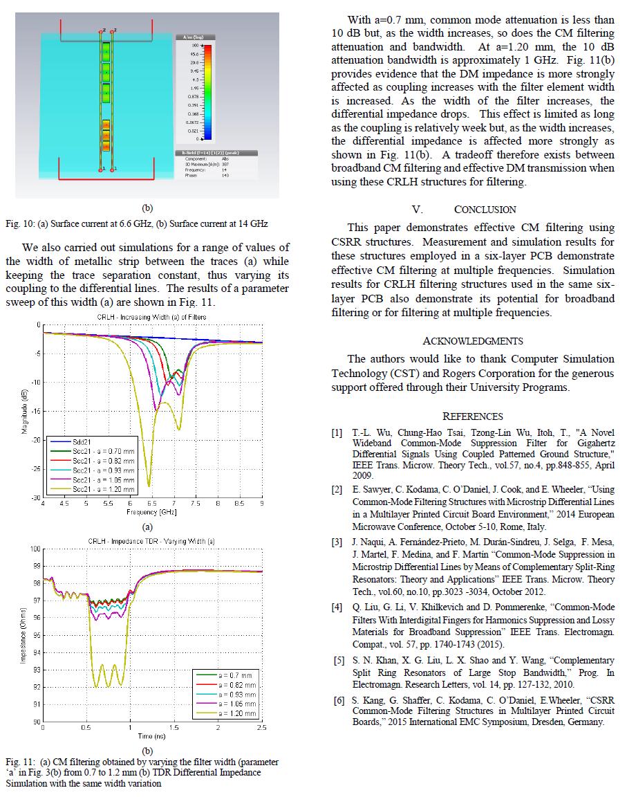
96 80

97 APPENDIX D Submitted Paper 81
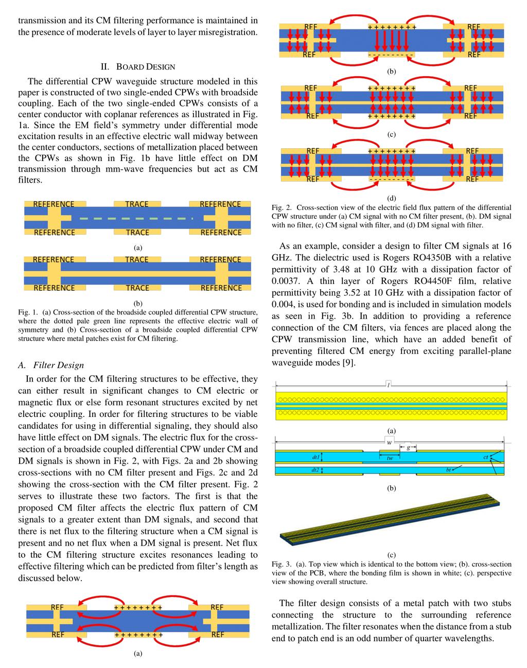
98 82
99 83
100 84
101 85
102 86
Introduction: Planar Transmission Lines
 Chapter-1 Introduction: Planar Transmission Lines 1.1 Overview Microwave integrated circuit (MIC) techniques represent an extension of integrated circuit technology to microwave frequencies. Since four
Designs of Substrate Integrated Waveguide (SIW) and Its Transition to Rectangular Waveguide. Ya Guo
 and Its Transition to Rectangular Waveguide. Ya Guo") Designs of Substrate Integrated Waveguide (SIW) and Its Transition to Rectangular Waveguide by Ya Guo A thesis submitted to the Graduate Faculty of Auburn University in partial fulfillment of the requirements
Designs of Substrate Integrated Waveguide (SIW) and Its Transition to Rectangular Waveguide by Ya Guo A thesis submitted to the Graduate Faculty of Auburn University in partial fulfillment of the requirements
RF AND MICROWAVE ENGINEERING
 RF AND MICROWAVE ENGINEERING FUNDAMENTALS OF WIRELESS COMMUNICATIONS Frank Gustrau Dortmund University of Applied Sciences and Arts, Germany WILEY A John Wiley & Sons, Ltd., Publication Preface List of
Practical Measurements of Dielectric Constant and Loss for PCB Materials at High Frequency
 8 th Annual Symposium on Signal Integrity PENN STATE, Harrisburg Center for Signal Integrity Practical Measurements of Dielectric Constant and Loss for PCB Materials at High Frequency Practical Measurements
CHAPTER 4. Practical Design
 CHAPTER 4 Practical Design The results in Chapter 3 indicate that the 2-D CCS TL can be used to synthesize a wider range of characteristic impedance, flatten propagation characteristics, and place passive
L-BAND COPLANAR SLOT LOOP ANTENNA FOR INET APPLICATIONS
 L-BAND COPLANAR SLOT LOOP ANTENNA FOR INET APPLICATIONS Jeyasingh Nithianandam Electrical and Computer Engineering Department Morgan State University, 500 Perring Parkway, Baltimore, Maryland 5 ABSTRACT
Waveguides. Metal Waveguides. Dielectric Waveguides
 Waveguides Waveguides, like transmission lines, are structures used to guide electromagnetic waves from point to point. However, the fundamental characteristics of waveguide and transmission line waves
Lecture #3 Microstrip lines
 November 2014 Ahmad El-Banna Benha University Faculty of Engineering at Shoubra Post-Graduate ECE-601 Active Circuits Lecture #3 Microstrip lines Instructor: Dr. Ahmad El-Banna Agenda Striplines Forward
Application Note 5525
 Using the Wafer Scale Packaged Detector in 2 to 6 GHz Applications Application Note 5525 Introduction The is a broadband directional coupler with integrated temperature compensated detector designed for
Chapter 3 Broadside Twin Elements 3.1 Introduction
 Chapter 3 Broadside Twin Elements 3. Introduction The focus of this chapter is on the use of planar, electrically thick grounded substrates for printed antennas. A serious problem with these substrates
EC Transmission Lines And Waveguides
 EC6503 - Transmission Lines And Waveguides UNIT I - TRANSMISSION LINE THEORY A line of cascaded T sections & Transmission lines - General Solution, Physical Significance of the Equations 1. Define Characteristic
APPLICATION NOTE FOR PA.700A ANTENNA INTEGRATION
 APPLICATION NOTE FOR PA.700A ANTENNA INTEGRATION VERSION A Your Global Source for RF, Wireless & Energy Technologies www.richardsonrfpd.com 800.737.6937 630.208.2700 APN-11-8-001/A 14-July-11 Page 1 of
Electromagnetics, Microwave Circuit and Antenna Design for Communications Engineering
 Electromagnetics, Microwave Circuit and Antenna Design for Communications Engineering Second Edition Peter Russer ARTECH HOUSE BOSTON LONDON artechhouse.com Contents Preface xvii Chapter 1 Introduction
Design of Microstrip Coupled Line Bandpass Filter Using Synthesis Technique
 Design of Microstrip Coupled Line Bandpass Filter Using Synthesis Technique 1 P.Priyanka, 2 Dr.S.Maheswari, 1 PG Student, 2 Professor, Department of Electronics and Communication Engineering Panimalar
Managing Complex Impedance, Isolation & Calibration for KGD RF Test Abstract
 Managing Complex Impedance, Isolation & Calibration for KGD RF Test Roger Hayward and Jeff Arasmith Cascade Microtech, Inc. Production Products Division 9100 SW Gemini Drive, Beaverton, OR 97008 503-601-1000,
COMPACT MICROSTRIP BANDPASS FILTERS USING TRIPLE-MODE RESONATOR
 Progress In Electromagnetics Research Letters, Vol. 35, 89 98, 2012 COMPACT MICROSTRIP BANDPASS FILTERS USING TRIPLE-MODE RESONATOR K. C. Lee *, H. T. Su, and M. K. Haldar School of Engineering, Computing
COMPACT SLOT ANTENNA WITH EBG FEEDING LINE FOR WLAN APPLICATIONS
 Progress In Electromagnetics Research C, Vol. 10, 87 99, 2009 COMPACT SLOT ANTENNA WITH EBG FEEDING LINE FOR WLAN APPLICATIONS A. Danideh Department of Electrical Engineering Islamic Azad University (IAU),
New Microstrip-to-CPS Transition for Millimeter-wave Application
 New Microstrip-to-CPS Transition for Millimeter-wave Application Kyu Hwan Han 1,, Benjamin Lacroix, John Papapolymerou and Madhavan Swaminathan 1, 1 Interconnect and Packaging Center (IPC), SRC Center
A 6 : 1 UNEQUAL WILKINSON POWER DIVIDER WITH EBG CPW
 Progress In Electromagnetics Research Letters, Vol. 8, 151 159, 2009 A 6 : 1 UNEQUAL WILKINSON POWER DIVIDER WITH EBG CPW C.-P. Chang, C.-C. Su, S.-H. Hung, and Y.-H. Wang Institute of Microelectronics,
Optically reconfigurable balanced dipole antenna
 Loughborough University Institutional Repository Optically reconfigurable balanced dipole antenna This item was submitted to Loughborough University's Institutional Repository by the/an author. Citation:
Circular Patch Antenna with CPW fed and circular slots in ground plane.
 Circular Patch Antenna with CPW fed and circular slots in ground plane. Kangan Saxena, USICT, Guru Gobind Singh Indraprastha University, Delhi-75 ---------------------------------------------------------------------***---------------------------------------------------------------------
Flip-Chip for MM-Wave and Broadband Packaging
 1 Flip-Chip for MM-Wave and Broadband Packaging Wolfgang Heinrich Ferdinand-Braun-Institut für Höchstfrequenztechnik (FBH) Berlin / Germany with contributions by F. J. Schmückle Motivation Growing markets
CHAPTER 2 MICROSTRIP REFLECTARRAY ANTENNA AND PERFORMANCE EVALUATION
 43 CHAPTER 2 MICROSTRIP REFLECTARRAY ANTENNA AND PERFORMANCE EVALUATION 2.1 INTRODUCTION This work begins with design of reflectarrays with conventional patches as unit cells for operation at Ku Band in
The Basics of Patch Antennas, Updated
 The Basics of Patch Antennas, Updated By D. Orban and G.J.K. Moernaut, Orban Microwave Products www.orbanmicrowave.com Introduction This article introduces the basic concepts of patch antennas. We use
Signal Integrity, Part 1 of 3
 by Barry Olney feature column BEYOND DESIGN Signal Integrity, Part 1 of 3 As system performance increases, the PCB designer s challenges become more complex. The impact of lower core voltages, high frequencies
ECE 4265/6265 Laboratory Project 7 Network Analyzer Calibration
 ECE 4265/6265 Laboratory Project 7 Network Analyzer Calibration Objectives The purpose of this lab is to introduce the concepts of calibration and error correction for microwave s-parameter measurements.
Department of Electrical Engineering University of North Texas
 Name: Shabuktagin Photon Khan UNT ID: 10900555 Instructor s Name: Professor Hualiang Zhang Course Name: Antenna Theory and Design Course ID: EENG 5420 Email: khan.photon@gmail.com Department of Electrical
Physical RF Circuit Techniques and Their Implications on Future Power Module and Power Electronic Design
 Physical RF Circuit Techniques and Their Implications on Future Power Module and Power Electronic Design Adam Morgan 5-5-2015 NE IMAPS Symposium 2015 Overall Motivation Wide Bandgap (WBG) semiconductor
insert link to the published version of your paper
 Citation Niels Van Thienen, Wouter Steyaert, Yang Zhang, Patrick Reynaert, (215), On-chip and In-package Antennas for mm-wave CMOS Circuits Proceedings of the 9th European Conference on Antennas and Propagation
A Novel Planar Microstrip Antenna Design for UHF RFID
 A Novel Planar Microstrip Antenna Design for UHF RFID Madhuri Eunni, Mutharasu Sivakumar, Daniel D.Deavours* Information and Telecommunications Technology Centre University of Kansas, Lawrence, KS 66045
EMC Simulation of Consumer Electronic Devices
 of Consumer Electronic Devices By Andreas Barchanski Describing a workflow for the EMC simulation of a wireless router, using techniques that can be applied to a wide range of consumer electronic devices.
APPLICATION NOTE FOR PA.710A ANTENNA INTEGRATION
 APPLICATION NOTE FOR PA.710A ANTENNA INTEGRATION APN-11-8-001/B Page 1 of 22 1. TABLE OF CONTENTS 1. TABLE OF CONTENTS... 2 2. BASICS... 4 3. APPLICATIONS... 5 4. IMPEDANCE... 5 5. BANDWIDTH... 5 6. GAIN...
Metamaterial Inspired CPW Fed Compact Low-Pass Filter
 Progress In Electromagnetics Research C, Vol. 57, 173 180, 2015 Metamaterial Inspired CPW Fed Compact Low-Pass Filter BasilJ.Paul 1, *, Shanta Mridula 1,BinuPaul 1, and Pezholil Mohanan 2 Abstract A metamaterial
Microwave Engineering
 Microwave Circuits 1 Microwave Engineering 1. Microwave: 300MHz ~ 300 GHz, 1 m ~ 1mm. a. Not only apply in this frequency range. The real issue is wavelength. Historically, as early as WWII, this is the
Comparison of IC Conducted Emission Measurement Methods
 IEEE TRANSACTIONS ON INSTRUMENTATION AND MEASUREMENT, VOL. 52, NO. 3, JUNE 2003 839 Comparison of IC Conducted Emission Measurement Methods Franco Fiori, Member, IEEE, and Francesco Musolino, Member, IEEE
Analysis of Microstrip Circuits Using a Finite-Difference Time-Domain Method
 Analysis of Microstrip Circuits Using a Finite-Difference Time-Domain Method M.G. BANCIU and R. RAMER School of Electrical Engineering and Telecommunications University of New South Wales Sydney 5 NSW
A Dual-Band Two Order Filtering Antenna
 Progress In Electromagnetics Research Letters, Vol. 63, 99 105, 2016 A Dual-Band Two Order Filtering Antenna Jingli Guo, Haisheng Liu *, Bin Chen, and Baohua Sun Abstract A dual-band two order filtering
Objectives of transmission lines
 Introduction to Transmission Lines Applications Telephone Cable TV (CATV, or Community Antenna Television) Broadband network High frequency (RF) circuits, e.g., circuit board, RF circuits, etc. Microwave
"Natural" Antennas. Mr. Robert Marcus, PE, NCE Dr. Bruce C. Gabrielson, NCE. Security Engineering Services, Inc. PO Box 550 Chesapeake Beach, MD 20732
 Published and presented: AFCEA TEMPEST Training Course, Burke, VA, 1992 Introduction "Natural" Antennas Mr. Robert Marcus, PE, NCE Dr. Bruce C. Gabrielson, NCE Security Engineering Services, Inc. PO Box
Challenges and Solutions for Removing Fixture Effects in Multi-port Measurements
 DesignCon 2008 Challenges and Solutions for Removing Fixture Effects in Multi-port Measurements Robert Schaefer, Agilent Technologies schaefer-public@agilent.com Abstract As data rates continue to rise
Broadband Circular Polarized Antenna Loaded with AMC Structure
 Progress In Electromagnetics Research Letters, Vol. 76, 113 119, 2018 Broadband Circular Polarized Antenna Loaded with AMC Structure Yi Ren, Xiaofei Guo *,andchaoyili Abstract In this paper, a novel broadband
APPLICATION NOTE FOR PA.710.A ANTENNA INTEGRATION
 APPLICATION NOTE FOR PA.710.A ANTENNA INTEGRATION APN-13-8-005/B/NB Page 1 of 17 1. TABLE OF CONTENTS 1. TABLE OF CONTENTS... 2 2. BASICS... 3 3. APPLICATIONS... 4 4. IMPEDANCE... 4 5. BANDWIDTH... 4 6.
Antenna Theory and Design
 Antenna Theory and Design Antenna Theory and Design Associate Professor: WANG Junjun 王珺珺 School of Electronic and Information Engineering, Beihang University F1025, New Main Building wangjunjun@buaa.edu.cn
A HIGH-POWER LOW-LOSS MULTIPORT RADIAL WAVEGUIDE POWER DIVIDER
 Progress In Electromagnetics Research Letters, Vol. 31, 189 198, 2012 A HIGH-POWER LOW-LOSS MULTIPORT RADIAL WAVEGUIDE POWER DIVIDER X.-Q. Li *, Q.-X. Liu, and J.-Q. Zhang School of Physical Science and
Research Article Compact and Wideband Parallel-Strip 180 Hybrid Coupler with Arbitrary Power Division Ratios
 Microwave Science and Technology Volume 13, Article ID 56734, 1 pages http://dx.doi.org/1.1155/13/56734 Research Article Compact and Wideband Parallel-Strip 18 Hybrid Coupler with Arbitrary Power Division
Microwave Metrology -ECE 684 Spring Lab Exercise T: TRL Calibration and Probe-Based Measurement
 ab Exercise T: TR Calibration and Probe-Based Measurement In this project, you will measure the full phase and magnitude S parameters of several surface mounted components. You will then develop circuit
EM Analysis of RFIC Transmission Lines
 EM Analysis of RFIC Transmission Lines Purpose of this document: In this document, we will discuss the analysis of single ended and differential on-chip transmission lines, the interpretation of results
Broadband low cross-polarization patch antenna
 RADIO SCIENCE, VOL. 42,, doi:10.1029/2006rs003595, 2007 Broadband low cross-polarization patch antenna Yong-Xin Guo, 1 Kah-Wee Khoo, 1 Ling Chuen Ong, 1 and Kwai-Man Luk 2 Received 27 November 2006; revised
TABEL OF CONTENTS. vii CHAPTER TITLE PAGE. TITLE i DECLARATION ii DEDICATION. iii ACKNOWLEDGMENT. iv ABSTRACT. v ABSTRAK vi TABLE OF CONTENTS
 vii TABEL OF CONTENTS CHAPTER TITLE PAGE TITLE i DECLARATION ii DEDICATION iii ACKNOWLEDGMENT iv ABSTRACT v ABSTRAK vi TABLE OF CONTENTS vii LIST OF TABLES xii LIST OF FIGURES xiii LIST OF SYMBOLS xvi
You will need the following pieces of equipment to complete this experiment: Wilkinson power divider (3-port board with oval-shaped trace on it)
") UNIVERSITY OF TORONTO FACULTY OF APPLIED SCIENCE AND ENGINEERING The Edward S. Rogers Sr. Department of Electrical and Computer Engineering ECE422H1S: RADIO AND MICROWAVE WIRELESS SYSTEMS EXPERIMENT 1:
UNIVERSITY OF TORONTO FACULTY OF APPLIED SCIENCE AND ENGINEERING The Edward S. Rogers Sr. Department of Electrical and Computer Engineering ECE422H1S: RADIO AND MICROWAVE WIRELESS SYSTEMS EXPERIMENT 1:
Introduction to Electromagnetic Compatibility
 Introduction to Electromagnetic Compatibility Second Edition CLAYTON R. PAUL Department of Electrical and Computer Engineering, School of Engineering, Mercer University, Macon, Georgia and Emeritus Professor
NH-67, TRICHY MAIN ROAD, PULIYUR, C.F , KARUR DT. DEPARTMENT OF ELECTRONICS AND COMMUNICATION ENGINEERING COURSE MATERIAL
 NH-67, TRICHY MAIN ROAD, PULIYUR, C.F. 639 114, KARUR DT. DEPARTMENT OF ELECTRONICS AND COMMUNICATION ENGINEERING COURSE MATERIAL Subject Name: Microwave Engineering Class / Sem: BE (ECE) / VII Subject
Plastic straw: future of high-speed signaling
 Supplementary Information for Plastic straw: future of high-speed signaling Ha Il Song, Huxian Jin, and Hyeon-Min Bae * Korea Advanced Institute of Science and Technology (KAIST), Department of Electrical
Study of Microstrip Slotted Antenna for Bandwidth Enhancement
 Global Journal of Researches in Engineering Electrical and Electronics Engineering Volume 2 Issue 9 Version. Type: Double Blind Peer Reviewed International Research Journal Publisher: Global Journals Inc.
INVENTION DISCLOSURE- ELECTRONICS SUBJECT MATTER IMPEDANCE MATCHING ANTENNA-INTEGRATED HIGH-EFFICIENCY ENERGY HARVESTING CIRCUIT
 INVENTION DISCLOSURE- ELECTRONICS SUBJECT MATTER IMPEDANCE MATCHING ANTENNA-INTEGRATED HIGH-EFFICIENCY ENERGY HARVESTING CIRCUIT ABSTRACT: This paper describes the design of a high-efficiency energy harvesting
UNIVERSITI MALAYSIA PERLIS
 UNIVERSITI MALAYSIA PERLIS SCHOOL OF COMPUTER & COMMUNICATIONS ENGINEERING EKT 341 LABORATORY MODULE LAB 2 Antenna Characteristic 1 Measurement of Radiation Pattern, Gain, VSWR, input impedance and reflection
MODELING AND CHARACTERIZATION OF 3D MULTILAYER TRANSMISSION LINES
 MODELING AND CHARACTERIZATION OF 3D MULTILAYER TRANSMISSION LINES A thesis submitted to The University of Manchester for the degree of MPhil In the Faculty of Engineering and Physical Sciences YEAR OF
Miniaturization of Harmonics-suppressed Filter with Folded Loop Structure
 PIERS ONINE, VO. 4, NO. 2, 28 238 Miniaturization of Harmonics-suppressed Filter with Folded oop Structure Han-Nien in 1, Wen-ung Huang 2, and Jer-ong Chen 3 1 Department of Communications Engineering,
CAD oriented study of Polyimide interface layer on Silicon substrate for RF applications
 CAD oriented study of Polyimide interface layer on Silicon substrate for RF applications Kamaljeet Singh & K Nagachenchaiah Semiconductor Laboratory (SCL), SAS Nagar, Near Chandigarh, India-160071 kamaljs@sclchd.co.in,
High-Speed Circuit Board Signal Integrity
 High-Speed Circuit Board Signal Integrity For a listing of recent titles in the Artech House Microwave Library, turn to the back of this book. High-Speed Circuit Board Signal Integrity Stephen C. Thierauf
ELEC Course Objectives/Proficiencies
 Lecture 1 -- to identify (and list examples of) intentional and unintentional receivers -- to list three (broad) ways of reducing/eliminating interference -- to explain the differences between conducted/radiated
A Signal Integrity Measuring Methodology in the Extraction of Wide Bandwidth Environmental Coefficients
 As originally published in the IPC APEX EXPO Conference Proceedings. A Signal Integrity Measuring Methodology in the Extraction of Wide Bandwidth Environmental Coefficients Eric Liao, Kuen-Fwu Fuh, Annie
The Ultimate Guide to Antenna Matching
 5 The Ultimate Guide to Antenna Matching 1 Contents Introduction 1. What is Antenna Matching? 2. The Importance of Trace Lines 3. Measures of Antenna Mismatches 4. Key Matching Considerations 5. Achieving
Microwave and RF Engineering
 Microwave and RF Engineering Volume 1 An Electronic Design Automation Approach Ali A. Behagi and Stephen D. Turner BT Microwave LLC State College, PA 16803 Copyrighted Material Microwave and RF Engineering
Texas Instruments DisplayPort Design Guide
 Texas Instruments DisplayPort Design Guide April 2009 1 High Speed Interface Applications Introduction This application note presents design guidelines, helping users of Texas Instruments DisplayPort devices
Γ L = Γ S =
 TOPIC: Microwave Circuits Q.1 Determine the S parameters of two port network consisting of a series resistance R terminated at its input and output ports by the characteristic impedance Zo. Q.2 Input matching
Design of Frequency and Polarization Tunable Microstrip Antenna
 Design of Frequency and Polarization Tunable Microstrip Antenna M. S. Nishamol, V. P. Sarin, D. Tony, C. K. Aanandan, P. Mohanan, K. Vasudevan Abstract A novel compact dual frequency microstrip antenna
ALMA MEMO #360 Design of Sideband Separation SIS Mixer for 3 mm Band
 ALMA MEMO #360 Design of Sideband Separation SIS Mixer for 3 mm Band V. Vassilev and V. Belitsky Onsala Space Observatory, Chalmers University of Technology ABSTRACT As a part of Onsala development of
Chapter 7 Design of the UWB Fractal Antenna
 Chapter 7 Design of the UWB Fractal Antenna 7.1 Introduction F ractal antennas are recognized as a good option to obtain miniaturization and multiband characteristics. These characteristics are achieved
APPLIED ELECTROMAGNETICS: EARLY TRANSMISSION LINES APPROACH
 APPLIED ELECTROMAGNETICS: EARLY TRANSMISSION LINES APPROACH STUART M. WENTWORTH Auburn University IICENTBN Nlfll 1807; WILEY 2 OO 7 ; Ttt^TlLtftiTTu CONTENTS CHAPTER1 Introduction 1 1.1 1.2 1.3 1.4 1.5
FILTERING ANTENNAS: SYNTHESIS AND DESIGN
 FILTERING ANTENNAS: SYNTHESIS AND DESIGN Deepika Agrawal 1, Jagadish Jadhav 2 1 Department of Electronics and Telecommunication, RCPIT, Maharashtra, India 2 Department of Electronics and Telecommunication,
Investigation of the Double-Y Balun for Feeding Pulsed Antennas
 Proceedings of the SPIE, Vol. 5089, April 2003 Investigation of the Double-Y Balun for Feeding Pulsed Antennas Jaikrishna B. Venkatesan a and Waymond R. Scott, Jr. b Georgia Institute of Technology Atlanta,
Microwave and optical systems Introduction p. 1 Characteristics of waves p. 1 The electromagnetic spectrum p. 3 History and uses of microwaves and
 Microwave and optical systems Introduction p. 1 Characteristics of waves p. 1 The electromagnetic spectrum p. 3 History and uses of microwaves and optics p. 4 Communication systems p. 6 Radar systems p.
Modeling of cable for measurements of small monopole antennas. Liu, L; Weng, YF; Cheung, SW; Yuk, TI; Foged, LJ
 Title Modeling of cable for measurements of small monopole antennas Author(s) Liu, L; Weng, YF; Cheung, SW; Yuk, TI; Foged, LJ Citation The 7th Loughborough Antennas and Propagation Conference (LAPC),
Wideband Bow-Tie Slot Antennas with Tapered Tuning Stubs
 Wideband Bow-Tie Slot Antennas with Tapered Tuning Stubs Abdelnasser A. Eldek, Atef Z. Elsherbeni and Charles E. Smith. atef@olemiss.edu Center of Applied Electromagnetic Systems Research (CAESR) Department
Design and Analysis of Wideband Patch Antenna for Dual band 2.4/5.8 GHz WLAN and WiMAX Application
 IOSR Journal of Electronics and Communication Engineering (IOSR-JECE) e-issn: 2278-2834,p- ISSN: 2278-8735.Volume 12, Issue 4, Ver. IV (Jul.-Aug. 2017), PP 59-65 www.iosrjournals.org Design and Analysis
A NEW PRINTED QUASI-LANDSTORFER ANTENNA
 A NEW PRINTED QUASI-LANDSTORFER ANTENNA A Thesis Submitted to the Graduate Faculty of the North Dakota State University of Agriculture and Applied Science By Masud Al Aziz In Partial Fulfillment of the
Lecture 4. Maximum Transfer of Power. The Purpose of Matching. Lecture 4 RF Amplifier Design. Johan Wernehag Electrical and Information Technology
 Johan Wernehag, EIT Lecture 4 RF Amplifier Design Johan Wernehag Electrical and Information Technology Design of Matching Networks Various Purposes of Matching Voltage-, Current- and Power Matching Design
Projects in microwave theory 2017
 Electrical and information technology Projects in microwave theory 2017 Write a short report on the project that includes a short abstract, an introduction, a theory section, a section on the results and
Citation Electromagnetics, 2012, v. 32 n. 4, p
 Title Low-profile microstrip antenna with bandwidth enhancement for radio frequency identification applications Author(s) Yang, P; He, S; Li, Y; Jiang, L Citation Electromagnetics, 2012, v. 32 n. 4, p.
CONTENTS. Note Concerning the Numbering of Equations, Figures, and References; Notation, xxi. A Bridge from Mathematics to Engineering in Antenna
 CONTENTS Note Concerning the Numbering of Equations, Figures, and References; Notation, xxi Introduction: Theory, 1 A Bridge from Mathematics to Engineering in Antenna Isolated Antennas 1. Free Oscillations,
Department of Technology and Built Environment
 Department of Technology and Built Environment Compact and Integrated Broadband Antennas for Wireless Applications Submitted by: Muhammad Afzal Sadiq (800202-T353) Supervisor: Dr.Hoshang Heydari Examiner
Keysight Technologies Signal Integrity Tips and Techniques Using TDR, VNA and Modeling
 Keysight Technologies Signal Integrity Tips and Techniques Using, VNA and Modeling Article Reprint This article first appeared in the March 216 edition of Microwave Journal. Reprinted with kind permission
Microwave Circuits 1.1 INTRODUCTION
 Microwave Circuits 1.1 INTRODUCTION The term microwave circuits means different things to different people. The prefix micro comes from the Greek fiikpog (micros) and among its various meanings has the
Power Dividers and Directional Couplers (7)
") Microwave Circuits 1 Power Dividers and Directional Couplers (7) The T-Junction Power Divider(7.2) Lossless Divider 1. Lossless 2. Match at the input port. 3. Mismatch at the output ports. 4. No isolation
Microwave Circuits 1 Power Dividers and Directional Couplers (7) The T-Junction Power Divider(7.2) Lossless Divider 1. Lossless 2. Match at the input port. 3. Mismatch at the output ports. 4. No isolation
A WIDEBAND RECTANGULAR MICROSTRIP ANTENNA WITH CAPACITIVE FEEDING
 A WIDEBAND RECTANGULAR MICROSTRIP ANTENNA WITH CAPACITIVE FEEDING Hind S. Hussain Department of Physics, College of Science, Al-Nahrain University, Baghdad, Iraq E-Mail: hindalrawi@yahoo.com ABSTRACT A
Internal Model of X2Y Chip Technology
 Internal Model of X2Y Chip Technology Summary At high frequencies, traditional discrete components are significantly limited in performance by their parasitics, which are inherent in the design. For example,
ON-CHIP TECHNOLOGY INDEPENDENT 3-D MOD- ELS FOR MILLIMETER-WAVE TRANSMISSION LINES WITH BEND AND GAP DISCONTINUITY
 Progress In Electromagnetics Research B, Vol. 22, 171 185, 2010 ON-CHIP TECHNOLOGY INDEPENDENT 3-D MOD- ELS FOR MILLIMETER-WAVE TRANSMISSION LINES WITH BEND AND GAP DISCONTINUITY G. A. Wang, W. Woods,
Exercise problems of topic 1: Transmission line theory and typical waveguides
 Exercise problems of topic 1: Transmission line theory and typical waveguides Return your answers in the contact sessions on a paper; either handwritten or typescripted. You can return them one by one.
MODIFIED MILLIMETER-WAVE WILKINSON POWER DIVIDER FOR ANTENNA FEEDING NETWORKS
 Progress In Electromagnetics Research Letters, Vol. 17, 11 18, 2010 MODIFIED MILLIMETER-WAVE WILKINSON POWER DIVIDER FOR ANTENNA FEEDING NETWORKS F. D. L. Peters, D. Hammou, S. O. Tatu, and T. A. Denidni
Millimetre-wave Phased Array Antennas for Mobile Terminals
 Millimetre-wave Phased Array Antennas for Mobile Terminals Master s Thesis Alberto Hernández Escobar Aalborg University Department of Electronic Systems Fredrik Bajers Vej 7B DK-9220 Aalborg Contents
Design and Improved Performance of Rectangular Micro strip Patch Antenna for C Band Application
 RESEARCH ARTICLE OPEN ACCESS Design and Improved Performance of Rectangular Micro strip Patch Antenna for C Band Application Vinay Jhariya*, Prof. Prashant Jain** *(Department of Electronics & Communication
Design of Linearly Polarized Rectangular Microstrip Patch Antenna for GPS Applications at MHz
 Design of Linearly Polarized Rectangular Microstrip Patch Antenna for GPS Applications at 1575.4MHz P. S. S. Pavan Ganesh Associate Professor, Sreyas Institute of Engineering and Technology, Hyderabad
Modeling and Simulation of Powertrains for Electric and Hybrid Vehicles
 Modeling and Simulation of Powertrains for Electric and Hybrid Vehicles Dr. Marco KLINGLER PSA Peugeot Citroën Vélizy-Villacoublay, FRANCE marco.klingler@mpsa.com FR-AM-5 Background The automotive context
Analysis and design of microstrip to balanced stripline transitions
 Analysis and design of microstrip to balanced stripline transitions RUZHDI SEFA 1, ARIANIT MARAJ 1 Faculty of Electrical and Computer Engineering, University of Prishtina - Prishtina Faculty of Software
Ultrawideband Elliptical Microstrip Antenna Using Different Taper Lines for Feeding
 Proceedings of the th WSEAS International Conference on COMMUNICATIONS, Agios Nikolaos, Crete Island, Greece, July 6-8, 007 44 Ultrawideband Elliptical Microstrip Antenna Using Different Taper Lines for
The number of layers The number and types of planes (power and/or ground) The ordering or sequence of the layers The spacing between the layers
 The ordering or sequence of the layers The spacing between the layers") PCB Layer Stackup PCB layer stackup (the ordering of the layers and the layer spacing) is an important factor in determining the EMC performance of a product. The following four factors are important with
PCB Layer Stackup PCB layer stackup (the ordering of the layers and the layer spacing) is an important factor in determining the EMC performance of a product. The following four factors are important with
Design Fundamentals by A. Ciccomancini Scogna, PhD Suppression of Simultaneous Switching Noise in Power and Ground Plane Pairs
 Design Fundamentals by A. Ciccomancini Scogna, PhD Suppression of Simultaneous Switching Noise in Power and Ground Plane Pairs Photographer: Janpietruszka Agency: Dreamstime.com 36 Conformity JUNE 2007
Advanced Transmission Lines. Transmission Line 1
 Advanced Transmission Lines Transmission Line 1 Transmission Line 2 1. Transmission Line Theory :series resistance per unit length in. :series inductance per unit length in. :shunt conductance per unit
Bandpass-Response Power Divider with High Isolation
 Progress In Electromagnetics Research Letters, Vol. 46, 43 48, 2014 Bandpass-Response Power Divider with High Isolation Long Xiao *, Hao Peng, and Tao Yang Abstract A novel wideband multilayer power divider