2.4 GHz TX / RX Booster With Diversity Switch for IoT / BLE / ZigBee
|
|
|
- Jacob Curtis
- 5 years ago
- Views:
Transcription
1 2.4 GHz TX / RX Booster With Diversity Switch for IoT / BLE / ZigBee NC DNC NC TXRX VDD VDD DNC DNC TXEN RXEN PDET Mode 10 SWant 15 IND 14 ANTA ANTB 11 DESCRIPTION The RFX2411N is a fully integrated, single-chip, single-die RFeIC (RF Front-end Integrated Circuit) which incorporates all the RF functionality needed for wireless ZigBee / smart energy applications. The RFX2411N architecture integrates a TX/RX and diversity switching circuitry with PA, LNA, and the associated matching networks with harmonic reduction all in a CMOS single-chip device. It also includes a bypass mode to provide maximal level of flexibility for system implementations. RFX2411N is designed for the 2.4GHz ISM band and supports standards like Bluetooth/BT EDR/ BLE, , ZigBee, ANT and Thread. RFX2411N is the perfect solution for applications requiring extended range and bandwidth. Typical high power applications include home and industrial automation, smart energy / smart metering, and RF4CE among others. RFX2411N interfaces seamless with low-voltage CMOS control logic, requires minimal external components, and provides even an integrated PA power detector circuit. Combining superior performance, high sensitivity, high efficiency, low noise, small form factor, low power consumtion and low cost, RFX2411N provides an ideal and application-friendly solution. FEATURES Single-Chip, Single-Die CMOS IC Transmit/Receive Switch Circuitry Antenna Diversity Switch Circuitry TX Power Amplifier or Bypass RX Low Noise Amplifier or Bypass Linearity Meeting Standards for OQPSK, DQPSK and 8DPSK Modulations Integrated Power Detector for Transmit Power Monitor and Control CMOS Control Logic ESD Protection Circuitry on All Pins RF Ports do not carry DC voltage Internal RF Decoupling on VDD Bias Pins Very Low DC Power Consumption Operation up to 125C o C ambient temperature Full On-chip Matching and Decoupling Circuitry Minimal External Components Required 50-Ohm Input / Output Matching Market Proven CMOS Technology 3 x 3 x 0.55mm Small Outline QFN-20 Package with Exposed Ground Pad APPLICATIONS Extended Range Devices ZigBee, ANT+, Thread, Bluetooth, BLE, RF4CE Smart Energy / Metering / Lighting / Remote Control Home and Industrial Automation Custom 2.4GHz Radio Systems Mobile and Battery Systems 1
2 PIN ASSIGNMENTS: Pin Number Pin Name Description 1, 11,13, 19, 21 Ground Must be connected to in the Application Circuit 2, 4 NC No Internal Connection Can be connected to in the Application Circuit 5 TXRX RF signal to/from the Transceiver (at DC this pin presents a short to ) 6 TXEN PA Control (digital CMOS input) 7 RXEN LNA Control (digital CMOS input) 8 PDET Analog output providing DC voltage proportional to PA RF Power Output 9 MODE BYPASS control (digital CMOS input ) 10 SWant ANTENNA control (digital CMOS input; selects between A and B for diversity) 12 ANTB PA Output / LNA Input for Ant B (at DC this pin presents a short to ) 14 ANTA PA Output / LNA Input for Ant A (at DC this pin presents a short to ) 15 IND Inductor to (choice of value impacts 2 nd harmonic) 3, 16, 17 DNC Reserved Do Not Connect at the PCB level in the Application Circuit 18, 20 VDD Voltage Supply (Internally Connected to each other) PIN-OUT DIAGRAM: VDD VDD DNC DNC NC DNC IND ANTA DNC 3 13 NC 4 12 ANTB TXRX TXEN RXEN PDET MODE SWANT 2
3 ABSOLUTE MAXIMUM RATINGS: Parameters Units Min Max Conditions DC VDD Voltage Supply V VDD Pins, Standby Mode DC Control Pin Voltage V DC VDD Current Consumption ma 350 Through VDD Pins when TX is ON TX RF Input Power dbm +5 LNA RF Input Power dbm +5 At active ANT port in RX LNA Mode Bypass RF Input Power dbm +16 At any RF port in Bypass mode Junction Temperature o C +150 Storage Ambient Temperature o C No RF and DC Voltages Applied Appropriate care required according to JEDEC Standards ESD HBM +/- V 3750 All Pins ESD CDM +/- V 1000 All Pins Note: Sustained operation at or above the Absolute Maximum Ratings for any one or combinations of the above parameters may result in permanent damage to the device and is not recommended. All Maximum RF Input Power Ratings assume 50-Ohm terminal impedance. RECOMENDED OPERATING CONDITIONS: Parameters Units Min Typ Max Conditions DC VDD Voltage Supply V 2.0* All VDD Pins Control Voltage High V 1.2 VDD 10K ohm series resistor Control Voltage Low V Control Pin DC Current Consumption na 300 MODE, TXEN, RXEN, SWANT DC Shutdown Current na 300 MODE, TXEN, RXEN = Low PA Turn On/Off Time µsec 1 LNA Turn On/Off Time µsec 1 Antenna Switch Time µsec 1 Operating Ambient Temperature o C ja o C/W 35 See Note 1 Note 1: For operation above +85 o C, use the ja as guidance for system design to assure the junction temperature will not exceed the maximum of +150 o C. A major contributor to ja is the PCB. The above ja value is based on the RFaxis EVB with multiple vias under the paddle. *At VDD < 3.3V the RFX2411N will provide a reduced maximum TX output power 3
4 PA TRANSMIT MODE PARAMETERS (VDD=3.3V; TXEN=High; Mode=Low; T=+25 o C) Parameters Units Min Typ Max Conditions Operating Frequency Band GHz All RF Pins Terminated by 50 Ohm Saturated Output Power dbm +21 Small-Signal Gain db 25 Harmonics (2 nd 5 th ) dbm/mhz POUT <= +20dBm; See application note for proper selection of pin 15 IND Total Supply Current ma 90 POUT = +20dBm TX Quiescent Current ma 20 TX Mode Input Return Loss db -10 Output Return Loss db -10 Power Detector Voltage mv Pout = +5 to +20dBm, 10kΩ load Input / Output Impedance Single-Ended Ohm 50 Load VSWR for Stability (Pout=20dBm) N/A 6:1 All Non-Harmonically Related Spurs < -53dBm/MHz Load VSWR for Ruggedness (Pout=20dBm) N/A 10:1 No Damage LNA RECEIVE MODE PARAMETERS (VDD=3.3V; RXEN=High; TXEN/Mode=Low;T=+25 o C) Parameters Units Min Typ Max Conditions Operating Frequency Band GHz All RF Pins Terminated by 50 Ohm Gain db 12 Noise Figure db 2.5 Input P1dB dbm -8 RX Quiescent Current ma 8 RF Port Impedance Ohm 50 At TXRX and ANT Pins Input Return Loss db -10 At ANT Pin Output Return Loss db -10 At TXRX Pin 4
5 BI-DIRECTIONAL BYPASS MODE PARAMETERS (VDD=3.3V; Mode=High; T=+25 o C): Parameters Units Min Typ Max Conditions Operating Frequency GHz Insertion Loss db 5 Input P1dB dbm 12 At ANTA or ANTB pin Total Current Consumption na 700 Mode = 2.0V, TX, RX = 0V CONTROL LOGIC TRUTH TABLE TXEN RXEN MODE Mode of Operation Shutdown Mode PA Transmit Mode LNA Receive Mode any any 1 Bypass Mode (bidirectional) SWant Mode of Operation 1 ANTA port enabled 0 ANTB port enabled Note: 1 denotes high voltage state (> 1.2V) 0 denotes low voltage stage (<0.3V) at Control Pins any denotes liberty to either apply 1 or 0 without change 5
6 0. 0. RFX2411N PCB LAND PATTERN 0.25mm 0.2 mm 0.4mm mm 1.7 mm x 1.7mm 3.5mm mm PACKAGE MARKING: Pin 1 Mark 2411N LLLL.L AAYYWW First Line Part Number Second Line Lot Number Third Line Date Code 6
7 PACKAGE DIMENSIONS: A A1 D2 D e b Dimensions (mm) A A1 b D D2 E E2 e L Min Nom Max Pin 1 Mark E Pin 1 L E2 7
8 TAPE AND REEL INFORMATION: 8
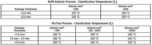
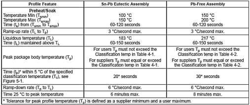
9 RECOMMENDED SOLDER REFLOW PROFILE 9
10 Mouser Electronics Authorized Distributor Click to View Pricing, Inventory, Delivery & Lifecycle Information: RFaxis: RFX2411N
CMOS 2.4GHZ ZIGBEE/ISM TRANSMIT/RECEIVE RFeIC
 CMOS 2.4GHZ ZIGBEE/ISM TRANSMIT/RECEIVE RFeIC Description 17 1 2 3 4 TXRX VDD VDD D 16 15 14 13 12 11 10 ANT 9 The RFX2401C is a fully integrated, single-chip, single-die RFeIC (RF Front-end Integrated
CMOS 2.4GHZ ZIGBEE/ISM TRANSMIT/RECEIVE RFeIC
 CMOS 2.4GHZ ZIGBEE/ISM TRANSMIT/RECEIVE RFeIC Description 17 1 2 3 4 TXRX VDD VDD D 16 15 14 13 12 11 10 ANT 9 The is a fully integrated, single-chip, single-die RFeIC (RF Front-end Integrated Circuit)
CMOS 2.4GHZ ZIGBEE/ISM TRANSMIT/RECEIVE RFeIC
 hot RFX2401C CMOS 2.4GHZ ZIGBEE/ISM TRANSMIT/RECEIVE RFeIC Description 1 2 3 4 TXRX 17 VDD VDD DNC 16 15 14 13 12 11 10 ANT 9 The RFX2401C is a fully integrated, single-chip, single-die RFeIC (RF Front-end
CMOS 5GHz WLAN ac RFeIC WITH PA, LNA AND SPDT
 CMOS 5GHz WLAN 802.11ac RFeIC WITH PA, LNA AND SPDT RX LEN 16 RXEN ANT 15 14 13 12 11 Description RFX8051 is a highly integrated, single-chip, single-die RFeIC (RF Front-end Integrated Circuit) which incorporates
CMOS 2.4GHZ TRANSMIT/RECEIVE WLAN RFeIC
 CMOS 2.4GHZ TRANSMIT/RECEIVE WLAN RFeIC 17 1 RX 2 3 VDD VDD DNC 16 15 14 13 12 11 10 ANT Description The RFX2402C is a fully integrated, single-chip, single-die RFeIC (RF Front-end Integrated Circuit)
CMOS 5GHz WLAN ac RFeIC WITH PA, LNA AND SPDT
 CMOS 5GHz WLAN 802.11ac RFeIC WITH PA, LNA AND SPDT RX LEN 16 RXEN ANT 15 14 13 12 11 Description RFX8051B is a highly integrated, single-chip, single-die RFeIC (RF Front-end Integrated Circuit) which
CMOS 5GHz WLAN a/n/ac RFeIC WITH PA, LNA, AND SPDT
 CMOS 5GHz WLAN 802.11a/n/ac RFeIC WITH PA, LNA, AND SPDT Description RX 1 2 LNA_EN 16 ANT 15 14 13 12 11 RFX8055 is a highly integrated, single-chip, single-die RFeIC (RF Front-end Integrated Circuit)
RFX2401C: 2.4 GHz Zigbee /ISM Front-End Module
 DATA SHEET RFX0C:. GHz Zigbee /ISM Front-End Module Applications ZigBee extended range devices ZigBee smart power Wireless sound and audio systems Home and industrial automation Wireless sensor networks
2.4GHZ CMOS WLAN / BT DUAL-MODE RFEIC WITH PA, LNA & SP3T
 2.4GHZ CMOS WLAN / BT DUAL-MODE RFEIC WITH PA, LNA & SP3T ANT DESCRIPTION DET VMODE 1 2 3 16 15 14 13 12 11 10 RFX8425 is a pure CMOS-based, single-chip/single-die RFeIC (RF Front-end Integrated Circuit)
RFX8050: CMOS 5 GHz WLAN ac RFeIC with PA, LNA, and SPDT
 DATA SHEET RFX8050: CMOS 5 GHz WLAN 802.11ac RFeIC with PA, LNA, and SPDT Applications 802.11a/n/ac Smartphones LEN RXEN ANT Tablets/MIDs Gaming Notebook/netbook/ultrabooks Mobile/portable devices RX Consumer
RFX8053: CMOS 5 GHz WLAN ac RFeIC with PA, LNA, and SPDT
 DATA SHEET RFX8053: CMOS 5 GHz WLAN 802.11ac RFeIC with PA, LNA, and SPDT Applications 802.11a/n/ac WiFi devices Smartphones Tablets/MIDs Gaming Consumer electronics Notebooks/netbooks/ultrabooks Mobile/portable
Range Extension for Nordic nrf51 Series with RFaxis RFX2411N RFeIC. Results Summary, Technical Notes and Application Schematic
 Range Extension for Nordic Series with RFaxis RFX2411N RFeIC Results Summary, Technical Notes and Application Schematic RFaxis Inc. August 2014 Range Extension with RFX2411N Contents Contents... 2 Figures...
RFX8425: 2.4 GHz CMOS WLAN/Bluetooth Dual-Mode RFeIC with PA, LNA, and SP3T
 DATA SHEET RFX8425: 2.4 GHz CMOS WLAN/Bluetooth Dual-Mode RFeIC with PA, LNA, and SP3T Applications Smartphones, feature phones. and MIDs with WLAN/Bluetooth WLAN/Bluetooth platforms requiring shared antenna
915MHz Transmit/Receive Module
 RF6599 915MHz Transmit/Receive Module This module is intended for 915MHz AMR solutions. It provides separate ports for Rx and Tx paths and two ports on the output for connecting a diversity solution or
RFFM V to 4.0V, 450MHz to 470MHz Transmit/Receive Front End Module
 .V to.0v, 0MHz to 0MHz Transmit/Receive Front End Module Package Style: LGA, 8-Pin,.mm x.0mm NC 8 Features Tx Output Power: 0dBm Tx Gain: 0dB Separate 0Ω Tx/Rx Transceiver Interface Rx Insertion Loss:
RF V TO 3.6V, 2.4GHz FRONT END MODULE
 3.V TO 3.6V, 2.4GHz FRONT END MODULE Package Style: QFN, 2-Pin, 3.mmx3.mmx.mm NC VBAT VBAT NC 4 3 2 Features Tx Output Power=22dBm Integrated RF Front End Module with TX/RX switch, PA, filter, and DP2T
RF V TO 4.2V, 2.4GHz FRONT END MODULE
 3.V TO 4.2V, 2.4GHz FRONT END MODULE Package Style: QFN, 2-Pin, 3.5mmx3.5mmx.5mm TXCT GND VCC_BAIS VCC NC 15 14 13 12 11 Features TX Output Power: 22dBm RX Gain: 11.5dB RX NF: 2.5dB Integrated RF Front
RFFM MHz Transmit/Receive Module
 925MHz Transmit/Receive Module This module is intended for 868MHz and 915MHz AMR solutions. The FEM provides separate ports for Rx/Tx paths, single-ended Tx and single-ended Rx or Rx differential port,
RFFM8500Q. 4.9GHz to 5.85GHz a/n Front End Module. Features. Applications. Ordering Information
 4.9GHz to 5.85GHz 802.11a/n Front End Module The RFFM8500Q provides a complete integrated solution in a single Front End Module (FEM) for WiFi 802.11a/n systems. The ultra small form factor and integrated
RFFM8511TR7. 4.9GHz to 5.85GHz a/n/ac WiFi Front End Module. Features. Applications. Ordering Information
 4.9GHz to 5.85GHz 802.11a/n/ac WiFi Front End Module The provides a complete integrated solution in a single front end module (FEM) for WiFi 802.11a/n/ac systems. The ultra-small factor and integrated
RFFM V to 5.0V, 2.4GHz to 2.5GHz b/g/n/ac WiFi Front End Module. Features. Applications. Ordering Information
 3.0V to 5.0V, 2.4GHz to 2.5GHz 802.11b/g/n/ac WiFi Front End Module The RFFM4293 provides a complete integrated solution in a single front end module (FEM) for WiFi 802.11b/g/n/ac and Bluetooth systems.
LNA VCC RX OUT TX IN VREG. Product Description. Ordering Information. Standard 25 piece bag Standard 2500 piece reel. GaAs HBT GaAs MESFET InGaP HBT
 2.4GHz TO 2.5GHz, 802.11b/g/n SINGLE-BAND FRONT END MODULE Package Style: QFN, 16-pin, 3.0 x 3.0 x 0.5 mm LNA EN C RX C TX BT 16 15 14 13 Features Single Module Radio Front- End Single Supply Voltage 3.0V
AWL a/n/ac Power Amplifier, LNA and Tx/Rx Switch DATA SHEET - Rev 2.0
 FEATURES Supports emerging 802.11ac high-data rate standard Fully integrated FEIC including 5GHz Power Amplifier, Low Noise Amplifier with Bypass mode and SP2T TX/RX Switch
RFFM V to 4.2V, ISM Band, 1W, 405MHz to 475MHz Transmit/Receive Module. Features. Applications. Ordering Information
 RFFM6403 2.5V to 4.2V, ISM Band, 1W, 405MHz to 475MHz Transmit/Receive Module The RFFM6403 is a single-chip front end module (FEM) for applications in the 405MHz and 475MHz ISM Bands. The RFFM6403 addresses
RF V TO 4.2V, 2.4GHz FRONT-END MODULE
 3.0V TO 4.2V, 2.4GHz FRONT-END MODULE Package Style: QFN, 20-Pin, 3.5mmx3.5mmx0.5mm Features TX Output Power: 22dBm TX Gain: 28dB RX Gain: 11.5dB RX NF: 2.5dB Integrated LNA With Bypass Mode Applications
Table of Contents 1. Typical Application General Description Feature PIN Configuration PIN Description (I: Input, O: O
 Document Title Data Sheet, with PA and LNA Revision History Rev. No. History Issue Date Remark 0.0 Initial issue. May, 2009 Objective 0.1 Change package from QFN3X3 12pin to QFN3X3 16 pin. Change mode
RFFM4503TR7. Features. Applications. Ordering Information. Package: Laminate, 16-pin, 3.0mm x 3.0mm x 1.0mm
 RFFM4503 4.9GHz to 5.85GHz 802.11a/n/ac Wi-Fi Front End Module The RFFM4503 provides a complete integrated solution in a single front end module (FEM) for Wi-Fi 802.11a/n/ac systems. The ultrasmall factor
MCP to 2.5 GHz RF Front End IC. Description
 Description The contains a power amplifier (PA), a low noise amplifier (LNA), and two SPDT switch. It is a 0-pins IC by 4 4mm -QFN package. RF input and output impedance of are 50Ω matched. Therefore,
RF V TO 4.0V,915MHz Transmit/Receive
 3.3V to 4.0V,9MHz Transmit/Receive Module RF639 3.3V TO 4.0V,9MHz Transmit/Receive Module Package: LGA, 8-Pin,.mm x.0mm Features Tx Output Power: dbm Separate 0 Tx/Rx Transceiver Interface Rx Insertion
AND0281. AND b/g/n/ac Power Amplifier, LNA and Tx/Rx/BT Switch PRELIMINARY DATA SHEET - Rev 1.2
 FEATURES Supports 802.11ac high-data rate standard Fully integrated FEIC including 2 GHz Power Amplifier, Low Noise Amplifier with Bypass mode and SP3T TX/RX/BT Switch 1.8% Dynamic EVM @ POUT = +18 dbm
DATA SHEET SE2431L: 2.4 GHz ZigBee/ Front-End Module Preliminary Datasheet. Product Description. Applications
 Applications Smart Meters In-home appliances Smart thermostats Features Integrated PA with up to 24 dbm output power Integrated LNA with programmable bypass Integrated antenna switching with Tx and Rx
RFFM8216TR7-5K. 2.4 GHz Integrated Wi-Fi Front-End Module
 RFFM8216 2.4 GHz Integrated Wi-Fi Front-End Module Product Overview The RFFM8216 provides a complete integrated solution in a single front end module (FEM) for WiFi 802.11b/g/n/ac systems.performance is
SKY : 2.4 GHz Transmit/Receive Front-End Module with Integrated Low-Noise Amplifier
 DATA SHEET SKY65344-21: 2.4 GHz Transmit/Receive Front-End Module with Integrated Low-Noise Amplifier Applications 2.4 GHz ISM band radios ZigBee FEMs IEEE 802.15.4 applications Features Transmit output
GND GND RFN BALUN RFP GND. Product Description. Ordering Information. Standard 2500 piece reel. GaAs HBT GaAs MESFET InGaP HBT
 RFFM0.0V TO.V,.GHZ FRONT END MODULE Package Style: Laminate, -Pin, mm x mm x mm C_RX_TX VCCLNA N/C ANTSEL 0 9 CE 8 Features Tx Output Power=dBm Integrated RF Front End Module with Balun, PA, filter, LNA
DATA SHEET SE2436L: High Power 2.4 GHz Front End Module. Product Description. Applications
 Applications Smart Meters In-home appliances Smart thermostats Features Integrated PA with 27 dbm output power Integrated LNA with programmable bypass Integrated antenna switching with Tx and Rx diversity
RF V to 4.2V, 2.4GHz Front End Module
 3.0V to 4.2V, 2.4GHz Front End Module Package Style: QFN, 20-Pin, 3.5mm x 3.5mm x 0.5mm TXCT _BAIS GND NC 15 14 13 12 11 Features TX Output Power: 23dBm TX Gain: 28dB RX Gain: 11.5dB RX NF: 3dB Integrated
TQM679002A Data Sheet
 Block Diagram Rxp Rxn PABC PAEN Tx in Pdetect BTH Balun Product Description PA Directional Detector BTSW RXSW TXSW ANT The TQM679002A is full WLAN/BT front-end module in an ultra small 3mm x 3mm footprint
Analog Devices Welcomes Hittite Microwave Corporation NO CONTENT ON THE ATTACHED DOCUMENT HAS CHANGED
 Analog Devices Welcomes Hittite Microwave Corporation NO CONTENT ON THE ATTACHED DOCUMENT HAS CHANGED www.analog.com www.hittite.com THIS PAGE INTENTIONALLY LEFT BLANK Typical Applications Transmit & Receive
Features OBSOLETE. = +25 C, Rbias = 0 Ohm. Bypass Mode Failsafe Mode Parameter
 7 Typical Applications The HMC668LP3(E) is ideal for: Cellular/3G and LTE/WiMAX/4G BTS & Infrastructure Repeaters and Femtocells Tower Mounted Amplifiers Test & Measurement Equipment Functional Diagram
GHz RF Front-End Module. o C
 Functional Block Diagram Features 4 High Efficient Power Amplifier: 41% at Pout= 23dBm -PA P-1dB: +21dBM Typical @ +3.3V-PA Low Noise Amplifier (NF typical 1.8dB)-LNA Low Insertion Loss:0.4dB@ 2.45GHz-Switch
RF V, SWITCH AND LNA FRONT END SOLUTION
 3.3V, SWITCH AND LNA FRONT END SOLUTION Package Style: QFN, -pin, 2mmx2mmx0.5mm C_BT 9 BT GND 7 Features Single Supply Voltage 3.0V to.5v Integrated SP3T Switch and LNA With Bypass Typical gain is db and
DATA SHEET SE2568U: 2.4 GHz High Efficiency Wireless LAN PA Preliminary Applications. Product Description. Features. Ordering Information
 Applications Product Description IEEE802.11b DSSS WLAN IEEE802.11g OFDM WLAN IEEE802.11n OFDM WLAN General Applications Features Dual Mode IEEE802.11b & IEEE802.11g Integrated PA, digital bias control,
SKY : 2.4 GHz Transmit/Receive Front-End Module
 DATA SHEET SKY65337-11: 2.4 GHz Transmit/Receive Front-End Module Applications 2.4 GHz ISM band radios ZigBee FEMs IEEE 802.15.4 applications Features Transmit output power > +20 dbm Bidirectional path
LNA In. Input Match. LNA Vref. LNA Sel. RX Switch. TX Switch GND. PA Vcc2 GND GND. PA Out. Product Description. GaAs HBT GaAs MESFET InGaP HBT
 3.0V to 4.2V, ISM Band Transmit/Receive Module with Diversity Transfer Switch RFFM6904 3.0V TO 4.2V, ISM BAND TRANSMIT/RECEIVE MODULE WITH DIVERSITY TRANSFER SWITCH Package: LGA, 32-pin, 8mm x 8mm x 1.2mm
OBSOLETE HMC915LP4E. GaAs MMIC MIXER w/ INTEGRATED LO AMPLIFIER, GHz. Typical Applications. Features. Functional Diagram. General Description
 v1.5 LO AMPLIFIER,.5-2.7 GHz Typical Applications The is ideal for: PCS / 3G Infrastructure Base Stations & Repeaters WiMAX & WiBro ISM & Fixed Wireless Functional Diagram Features Input IP3: +28 dbm Low
HFA GHz - 2.5GHz 250mW Power Amplifier. Description. Features. Applications. Ordering Information. Functional Block Diagram
 SEMICONDUCTOR HFA39 January 1997 2.4GHz - 2.GHz mw Power Amplifier Features Highly Integrated Power Amplifier with T/R Switch Operates Over 2.7V to Supply Voltage High Linear Output Power (P 1dB : +24dBm)
Features. Gain: 14.5 db. Electrical Specifications [1] [2] = +25 C, Rbias = 825 Ohms for Vdd = 5V, Rbias = 5.76k Ohms for Vdd = 3V
![Features. Gain: 14.5 db. Electrical Specifications [1] [2] = +25 C, Rbias = 825 Ohms for Vdd = 5V, Rbias = 5.76k Ohms for Vdd = 3V](/thumbs/90/101370216.jpg "Features. Gain: 14.5 db. Electrical Specifications [1] [2] = +25 C, Rbias = 825 Ohms for Vdd = 5V, Rbias = 5.76k Ohms for Vdd = 3V") Typical Applications The HMC77ALP3E is ideal for: Fixed Wireless and LTE/WiMAX/4G BTS & Infrastructure Repeaters and Femtocells Public Safety Radio Access Points Functional Diagram Features Noise Figure:.
Typical Applications The HMC77ALP3E is ideal for: Fixed Wireless and LTE/WiMAX/4G BTS & Infrastructure Repeaters and Femtocells Public Safety Radio Access Points Functional Diagram Features Noise Figure:.
MPQ20051-AEC1 Low Noise, High PSRR, 1A Linear Regulator AEC-Q100 Qualified
 MPQ20051-AEC1 Low Noise, High PSRR, 1A Linear Regulator AEC-Q100 Qualified DESCRIPTION The MPQ20051 is a low-dropout linear regulator that supplies up to 1A current with a 140mV dropout voltage. The externally-adjustable
HMC618ALP3E AMPLIFIERS - LOW NOISE - SMT. GaAs SMT phemt LOW NOISE AMPLIFIER, GHz. Typical Applications. Features. Functional Diagram
 7 Typical Applications The is ideal for: Cellular/3G and LTE/WiMAX/4G BTS & Infrastructure Repeaters and Femto Cells Public Safety Radios Functional Diagram v. Electrical Specifications T A = + C, Rbias
Features. = +25 C, Vdd 1, 2, 3 = +3V
 v.11 HMC6LC AMPLIFIER, 6-2 GHz Typical Applications The HMC6LC is ideal for use as a LNA or driver amplifier for: Point-to-Point Radios Point-to-Multi-Point Radios & VSAT Test Equipment and Sensors Military
RF V TO 4.0V, 915MHz TRANSMIT/RECEIVE MODULE
 RF6693.1V to 4.V, 91MHz Transmit/Receive Module RF669 3.1V TO 4.V, 91MHz TRANSMIT/RECEIVE MODULE Package: LGA, 28-Pin,.mm x.mm ASW_RX BAL_IN 1 28 27 26 2 24 23 22 Features Tx Output Power: 3dBm NC 2 3
DATA SHEET SE2432L: 2.4 GHz Smart Energy/ZigBee Front End Module. Product Description. Applications
 Applications Smart Meters In-home appliances Smart thermostats Features Integrated PA with up to 24 dbm output power Integrated LNA with programmable bypass Integrated antenna switching with Tx and Rx
SAW BPF SW2_OUT GND GND 868/915 RFIO SW2 GND 450 RFIO GND CTL1 CTL2 CTL LOGIC CTL3 CTL4 CTL5 VDIG. Product Description. Ordering Information
 2.7V to 4.4V, 9MHz Transmit/Receive Module; Thru Mode 4MHz to 928MHz RF6549 2.7V to 4.4V, 9MHz Transmit/Receive Module; Thru Mode 4MHz to 928MHz Package: LGA, 32-Pin, 6mm x 6mm TX TX SAW BPF SAW BPF SW2_OUT
SKY : 2.4 GHz ZigBee /Thread/Bluetooth Front-End Module
 DATA SHEET SKY6643-11: 2.4 GHz ZigBee /Thread/Bluetooth Front-End Module Applications In-home appliances CSD CPS CRX CTX CHL ANT_SEL Smart thermostats Internet of Things (IoT) devices Smart lighting Sensors
Features. = +25 C, Vdd = +10 V, Idd = 350 ma
 HMC97APME v2.4 POWER AMPLIFIER,.2-22 GHz Typical Applications The HMC97APME is ideal for: Test Instrumentation Military & Space Functional Diagram Features High P1dB Output Power: + dbm High : 14 db High
QPF4206BTR7. Wi-Fi Front End Module. Product Overview. Key Features. Functional Block Diagram. Applications. Ordering Information PRELIMINARY
 Product Overview The Qorvo is an integrated front end module (FEM) designed for Wi-Fi 802.11ax systems. The compact form factor and integrated matching minimizes layout area in the application. Performance
MADR V to 250V Driver for High Power PIN Diode Switches Rev. V1. Functional Schematic. Features. Description. Pin Configuration 1
 Features 20 V to 250 V Back Bias in Off State 200 ma Series Diode Bias Current at +25 C 50 ma Shunt Diode Bias Current at +25 C Propagation Delay less than 8 µs Low Quiescent Current Consumption 3 V or
Features. = +25 C, Vdd = +15V, Vgg2 = +9.5V [1], Idq = 500 ma [2]
![Features. = +25 C, Vdd = +15V, Vgg2 = +9.5V [1], Idq = 500 ma [2]](/thumbs/88/115381636.jpg "Features. = +25 C, Vdd = +15V, Vgg2 = +9.5V [1], Idq = 500 ma [2]") v3.41 Typical Applications Features The is ideal for: Test Instrumentation Military & Space Fiber optics Functional Diagram P1dB Output Power: + dbm Psat Output Power: + dbm High Gain: db Output IP3: 42
v3.41 Typical Applications Features The is ideal for: Test Instrumentation Military & Space Fiber optics Functional Diagram P1dB Output Power: + dbm Psat Output Power: + dbm High Gain: db Output IP3: 42
SKY : 2.4 GHz Transmit/Receive Front-End Module with Integrated LNA
 DATA SHEET SKY65336-11: 2.4 GHz Transmit/Receive Front-End Module with Integrated LNA Applications 2.4 GHz ISM band radios ZigBee FEMs IEEE 802.15.4 applications Features Transmit output power > +20 dbm
Product Description VG111-F
 Gain Ctrl Product Features 1.7 2.7 GHz bandwidth 26.6 db Attenuation Range +39.5 dbm Output IP3 +22 dbm P1dB Constant IP3 & P1dB over attenuation range Single voltage supply Pb-free 6mm 2-pin QFN package
DATA SHEET SE2576L: 2.4 GHz High Power Wireless LAN Power Amplifier Preliminary. Product Description. Applications. Features. Ordering Information
 Applications IEEE802.11b DSSS WLAN IEEE802.11g,n OFDM WLAN Access Points Features Dual Mode IEEE802.11b, IEEE802.11g, IEEE802.11n 26 dbm, EVM = 3%, 802.11g, OFDM 54 Mbps 29 dbm, 802.11b mask compliant
1.9GHz Power Amplifier
 EVALUATION KIT AVAILABLE MAX2248 General Description The MAX2248 single-supply, low-voltage power amplifier (PA) IC is designed specifically for applications in the 188MHz to 193MHz frequency band. The
SKY : 900 MHz Transmit/Receive Front-End Module
 DATA SHEET SKY65313-21: 900 MHz Transmit/Receive Front-End Module Applications Automated meter reading Advanced metering infrastructure ISM systems Features Transmit output power > +30.5 dbm High efficiency
AWL GHz b/g/n WLAN PA, LNA, and RF Switch Data Sheet - Rev 2.0
 . GHz.11b/g/n WLAN PA, LNA, and RF Switch Data Sheet Rev. FEATURES 3.3 % EVM @ POUT = +1 dbm with IEEE.11g QAM OFDM at 5 Mbps 75 ma Transmit Path Current Consumption at POUT = +1 dbm SP3T RF Switch to
GHz RF Front-End Module (Low Current) Note: All information provided is subjected to change without prior notice.
 Note: All information provided is subjected to change without prior notice.") Preliminary FM2422 dual-mode 82.11 b/g RF Front-End Module QFN WH378 Rev. 1 2.4-2.5 GHz RF Front-End Module (Low Current) Note: All information provided is subjected to change without prior notice. Product
Preliminary FM2422 dual-mode 82.11 b/g RF Front-End Module QFN WH378 Rev. 1 2.4-2.5 GHz RF Front-End Module (Low Current) Note: All information provided is subjected to change without prior notice. Product
ADG918/ADG919. Wideband 4 GHz, 43 db Isolation at 1 GHz, CMOS 1.65 V to 2.75 V, 2:1 Mux/SPDT FEATURES FUNCTIONAL BLOCK DIAGRAMS APPLICATIONS
 Wideband 4 GHz, 43 db Isolation at 1 GHz, CMOS 1.65 V to 2.75 V, 2:1 Mux/SPDT ADG918/ FEATURES Wideband switch: 3 db @ 4 GHz Absorptive/reflective switches High off isolation (43 db @ 1 GHz) Low insertion
MP MHz, 700mA, Fixed-Frequency Step-Up Driver for up to 10 White LEDS
 MP3301 1.3MHz, 700mA, Fixed-Frequency Step-Up Driver for up to 10 White LEDS DESCRIPTION The MP3301 is a step-up converter designed to drive WLEDS arrays from a single-cell, lithium-ion battery. The MP3301
SKY : 2.4 GHz Front-End Module for Bluetooth Low Energy / /Thread/ZigBee
 DATA SHEET SKY66114-11: 2.4 GHz Front-End Module for Bluetooth Low Energy /802.15.4/Thread/ZigBee Applications CSD CPS CRX CTX CHL In-home appliances Smart thermostats IoT gateways PA 21/16/13 dbm Logic
190μA, 3MHz, Rail-to-Rail I/O CMOS Operational Amplifiers VREF. DIO2026QN20 D2026 RoHS/Green -40 to +125 C QFN4*4-20 Tape & Reel, 5000
 Rev 0.1 DIO2026 190μA, 3MHz, Rail-to-Rail I/O CMOS Operational Amplifiers Features Supply Voltage Range: 2.5V to 5.5V Supply Current: Typical 190μA per channel Rail-to-Rail Input and Output ±1mV Typical
SKY : 2.4 GHz ZigBee /Thread/Bluetooth Smart Front-End Module
 DATA SHEET SKY661-11: 2.4 GHz ZigBee /Thread/Bluetooth Smart Front-End Module Applications In-home appliances Smart thermostats Internet of Things (IoT) devices Smart lighting Sensors Range extender Features
MPQ8904 Industrial/Automotive-Grade 500mA Linear Regulator AEC-Q100 Qualified
 The Future of Analog IC Technology DESCRIPTION The MPQ90 is a low-current, low-dropout, linear regulator that operates on a single 2.Vto-.V input supply. An external resistor controls the output voltage.
SE2431L: 2.4 GHz ZigBee / Front-End Module
 DATA SHEET SE431L:.4 GHz ZigBee /0.15.4 Front-End Module Applications Smart meters In-home appliances Smart thermostats Features Integrated: PA with up to +4 dbm output power LNA with programmable bypass
H/L Lin. Bias, Enable, Detector Circuits. Note: The TXIN has a DC short to ground. An external blocking capacitor is recommended at the TXIN port.
 Applications 5 GHz WLAN (IEEE802.11a/g/n) Access Points, PCMCIA, PC cards Features 5GHz Front End Module with PA, LNA and T/R Switch Integrated power amplifier enable pin (VEN) Buffered, temperature compensated
RFPA V 2.4GHz to 2.5GHz Matched Power Amplifier
 5.0V 2.4GHz to 2.5GHz Matched Power Amplifier Package: Laminate, 14-pin,7mm x 7mm x 1mm VCC 1 14 VCC3 PA_EN 2 13 Features P OUT = 29dBm; EVM = 3%; 11n MCS7 HT40 Input and Output Matched to 50Ω High Gain:
MSW2T /MSW2T /MSW2T SP2T Surface Mount High Power PIN Diode Switch
 PRELIMINARY MSW2T-2000-199/MSW2T-2001-199/MSW2T-2002-199 SP2T Surface Mount High Power PIN Diode Switch Features: Wide Operating Frequency Band: 50 MHz to 6 GHz Surface Mount SP2T Switch 5mm x 8mm x 2.5mm
MAAM Wideband Amplifier 10 MHz - 40 GHz Rev. V2. Features. Functional Schematic. Description. Pin Configuration. Ordering Information 1,2
 MAAM-1119 1 MHz - 4 GHz Rev. V2 Features 13 db Gain Ω Input / Output Match +18 dbm Output Power + V DC, 19 ma Lead-Free mm 9-lead LGA Package RoHS* Compliant and 26 C Reflow Compatible Description The
DOCSIS 3.0 Upstream Amplifier
 General Description The MAX3519 is an integrated CATV upstream amplifier IC designed to exceed the DOCSIS 3.0 requirements. The amplifier covers a 5MHz to 85MHz input frequency range (275MHz, 3dB bandwidth),
QPF4200SR. Wi-Fi Front End Module. Product Overview. Key Features. Functional Block Diagram. Applications. Ordering Information
 Product Overview The Qorvo QPF4200 is an integrated front end module (FEM) designed for Wi-Fi 802.11ax systems. The compact form factor and integrated matching minimizes layout area in the application.
INNOTION YP GHz-2.7GHz High Linearity Power Amplifier
 Features 3dB Gain(Typ) 33dBm P -1dB @ VCC=V NC VCC1 VCC2 NC 16 1 14 13 RoHS & Pb-Free Product 2.% EVM WLAN @Pout=27dBm, VCC=V 3mA Quiescent Current@ VCC=V.V DC Operation Integrated Output Power Detector
ADG918/ADG919. Wideband 4 GHz, 43 db Isolation at 1 GHz, CMOS 1.65 V to 2.75 V, 2:1 Mux/SPDT Switches
 Wideband 4 GHz, 43 db Isolation at 1 GHz, CMOS 1.65 V to 2.75 V, 2:1 Mux/SPDT Switches ADG918/ FEATURES Wideband switch: 3 db @ 4 GHz Absorptive/reflective switches High off isolation (43 db @ 1 GHz) Low
IDTF2255NLGK8. IDTF2255NLGK Datasheet GENERAL DESCRIPTION FEATURES COMPETITIVE ADVANTAGE DEVICE BLOCK DIAGRAM ORDERING INFORMATION APPLICATIONS
 1MHz to 3MHz GENERAL DESCRIPTION The IDTF2255 is a low insertion loss Voltage Variable RF Attenuator (VVA) designed for a multitude of wireless and other RF applications. This device covers a broad frequency
GHz Low-Noise Amplifier SST12LN01
 FEATURES: SST2L APPLICATIONS: Suitable Gain: Typically 4 db gain across 2.4 2.5 GHz Low-Noise Figure: Typically.55 db across 2.4 2.5 GHz IIP3: >dbm across 2.4 2.5 GHz Low-Current Consumption -2 ma across
FAN MHz TinyBoost Regulator with 33V Integrated FET Switch
 FAN5336 1.5MHz TinyBoost Regulator with 33V Integrated FET Switch Features 1.5MHz Switching Frequency Low Noise Adjustable Output Voltage Up to 1.5A Peak Switch Current Low Shutdown Current:
Features. Parameter Min Typ. Max Min Typ. Max Min Typ Max Units Frequency Range GHz Gain
 Typical Applications The HMC82LP4E is ideal for: Point-to-Point Radios Point-to-Multi-Point Radios VSAT & SATCOM Marine Radar Military EW & ECM Functional Diagram Features High Saturated Output Power:
TQP Preliminary Data Sheet
 Functional Block Diagram Product Description The TQP770001 Bluetooth PA is designed on TriQuint s advanced InGaP HBT GaAs technology offering state of the art reliability, temperature stability and ruggedness.
HMC6380LC4B. WIDEBAND VCOs - SMT. Electrical Specifications, T A. Typical Applications. Features. General Description. Functional Diagram
 Typical Applications Low Noise wideband MMIC VCO is ideal for: Industrial/Medical Equipment Test & Measurement Equipment Satcom Military Radar, EW, & ECM Functional Diagram Features Wide Tuning Bandwidth
SKY LF: 10 MHz GHz Six-Bit Digital Attenuator with Driver (0.5 db LSB, 31.5 db Range)
") DATA SHEET SKY12353-470LF: 10 MHz - 1.0 GHz Six-Bit Digital Attenuator with Driver (0.5 db LSB, 31.5 db Range) Applications Cellular base stations Wireless data transceivers Broadband systems Features
DATA SHEET SKY12353-470LF: 10 MHz - 1.0 GHz Six-Bit Digital Attenuator with Driver (0.5 db LSB, 31.5 db Range) Applications Cellular base stations Wireless data transceivers Broadband systems Features
RF3241SR. RF3241 Quad-Band GSM, Polar EDGE Transmit Module, Six UMTS TRX Switch Ports
 Quad-Band GSM, Polar EDGE Transmit Module, Six UMTS TRX Switch Ports The RF3241 is a quad-band GSM/GPRS, Polar EDGE transmit module with six interchangeable RF switch ports. The power amplifier supports
Features. = +25 C, IF = 100 MHz, LO = +13 dbm, LSB [1]
![Features. = +25 C, IF = 100 MHz, LO = +13 dbm, LSB [1]](/thumbs/85/92081906.jpg "Features. = +25 C, IF = 100 MHz, LO = +13 dbm, LSB [1]") v1.6 3.5 - GHz Typical Applications The HMC21BMSGE is ideal for: Base stations, Repeaters & Access Points WiMAX, WiBro & Fixed Wireless Portables & Subscribers PLMR, Public Safety & Telematics Functional
v1.6 3.5 - GHz Typical Applications The HMC21BMSGE is ideal for: Base stations, Repeaters & Access Points WiMAX, WiBro & Fixed Wireless Portables & Subscribers PLMR, Public Safety & Telematics Functional
SKY : Power Amplifier for a WLAN Applications
 DATA SHEET SKY65137-11: Power Amplifier for 802.11a WLAN Applications Applications IEEE802.11a WLAN enabled: access points media gateways set top boxes LCD TVs Other broadband triple-play multimedia applications
MSW2T /MSW2T SP2T Surface Mount High Power PIN Diode Switch
 RELEASED MSW2T-2040-193/MSW2T-2041-193 SP2T Surface Mount High Power PIN Diode Switch Features: Wide Operating Frequency Band: 50 MHz to 4 GHz Surface Mount SP2T Switch: 5mm x 8mm x 2.5mm Industry Leading
ESD Sensitive Component!!
 5 MHz LOW NOISE AMPLIFIER WHM3AE 1 REV E WHM3AE LNA is a low noise figure, wideband, and high linear SMT packaged amplifier with exceptional gain flatness design. The amplifier offers typical.7 db noise
MCP to 2.5 GHz RF Front End IC. Description
 Description The contains a power amplifier (PA), a low noise amplifier (), and two SPDT switch. It is a 0pins IC by 4 4mm QFN package. RF input and output impedance of are 50Ω matched. Therefore, precious
Not For New Design FMS W GaAs phemt SPDT SWITCH. Product Description. Features. Applications
 10W GaAs phemt SPDT Switch FMS2031-001 10W GaAs phemt SPDT SWITCH Package: 3 mm x 3 mm QFN Product Description The FMS2031-001 is a 10 W, Single-pole, Double-throw, (SPDT) GaAs phemt reflective antenna
TABLE OF CONTENTS Specifications... 3 Absolute Maximum Ratings... 4 ESD Caution... 4 Pin Configurations and Function Descriptions... 5 Terminology...
 FEATURES Wideband switch: 3 db @ 2.5 GHz ADG904: absorptive 4:1 mux/sp4t ADG904-R: reflective 4:1 mux/sp4t High off isolation (37 db @ 1 GHz) Low insertion loss (1.1 db dc to 1 GHz) Single 1.65 V to 2.75
400 MHz 4000 MHz Low Noise Amplifier ADL5521
 FEATURES Operation from 400 MHz to 4000 MHz Noise figure of 0.8 db at 900 MHz Including external input match Gain of 20.0 db at 900 MHz OIP3 of 37.7 dbm at 900 MHz P1dB of 22.0 dbm at 900 MHz Integrated
1 MHz to 2.7 GHz RF Gain Block AD8354
 Data Sheet FEATURES Fixed gain of 2 db Operational frequency of 1 MHz to 2.7 GHz Linear output power up to 4 dbm Input/output internally matched to Ω Temperature and power supply stable Noise figure: 4.2
H/L Lin. Bias, Enable, Detector Circuits. Match & Filter. TXIN and ANT are DC Blocked. However external blocking cap is recommended for RX output.
 Applications 5 GHz WLAN (IEEE802.11a/g/n) Access Points, PCMCIA, PC cards, Handhelds Features 5GHz Front End Module with PA, LNA and T/R Switch Integrated power amplifier enable pin (VEN) Buffered, temperature
HMC310MS8G / 310MS8GE. Features OBSOLETE. = +25 C, Vdd = +3V
 Typical Applications Transmit & Receive Switch for 2. GHz Applications: Bluetooth HomeRF WLAN Radios Functional Diagram v3.67 Electrical Specifications, T A = +25 C, Vdd = +3V HMC31MSG / 31MSGE Features
TOP VIEW IF LNAIN IF IF LO LO
 -3; Rev ; / EVALUATION KIT AVAILABLE Low-Cost RF Up/Downconverter General Description The performs the RF front-end transmit/ receive function in time-division-duplex (TDD) communication systems. It operates