RFFM8500Q. 4.9GHz to 5.85GHz a/n Front End Module. Features. Applications. Ordering Information
|
|
|
- Dale Hopkins
- 5 years ago
- Views:
Transcription

1 4.9GHz to 5.85GHz a/n Front End Module The RFFM8500Q provides a complete integrated solution in a single Front End Module (FEM) for WiFi a/n systems. The ultra small form factor and integrated matching minimizes the layout area in the customer's application and greatly reduces the number of external components. This simplifies the total front end solution by reducing the bill of materials, system footprint, and manufacturability cost. The RFFM8500Q integrates a Power Amplifier (PA), Single Pole Double Throw switch (SPDT), LNA and a power detector coupler for improved accuracy. The device is provided in a 3mm x 3mm x 1.0mm, 16-pin laminate package. This module meets or exceeds the RF Front End needs of IEEE a/n WiFi RF systems. The RFFM8500Q is tested in accordance with the AEC-Q100 Standard. LNA_EN 16 C_RX 15 ANT RFFM8500Q Package: Laminate, 16-pin, 3.0mm x 3.0mm x 1.05mm Features Tested in Accordance with AEC- Q100 Standard Single Supply Voltage 3.0V to 4.8V Integrated 5GHz Amplifier, SPT2T TX/RX Switch, LNA, and Power Detector Coupler P OUT = 16dBm, 11n, 2% Dynamic EVM; 3.3V Applications Automotive WiFi WiFi Direct Automotive Diagnostics WiFi Infotainment RX 2 11 VCC 3 10 VCC VDD 4 9 N/C TX N/C PA_EN Pdet Functional Block Diagram Ordering Information RFFM8500Q Standard 5-piece sample bag RFFM8500QSQ Standard 25-piece sample bag RFFM8500QSR Standard 100-piece reel RFFM8500QTR7 Standard 2500-piece reel RFFM8500QPCBA-410 Fully assembled evaluation board RF MICRO DEVICES and RFMD are trademarks of RFMD, LLC. BLUETOOTH is a trademark owned by Bluetooth SIG, Inc., U.S.A. and licensed for use by RFMD. All other trade names, trademarks, and registered trademarks are the property of their respective owners. 2013, RF Micro Devices, Inc. 1 of 10
 5 dbm Operating Ambient Temperature -40 to +85 C Storage Temperature -40 to +150 C Moisture Sensitivity MSL3 Nominal Operating Parameters RFMD Green:")
2 Absolute Maximum Ratings Parameter Rating Unit Caution! ESD sensitive device. DC Supply Voltage 5.5 V DC Maximum TX and RX Input Power (No Damage) 5 dbm Operating Ambient Temperature -40 to +85 C Storage Temperature -40 to +150 C Moisture Sensitivity MSL3 Nominal Operating Parameters RFMD Green: RoHS status based on EU Directive 2011/65/EU (at time of this document revision), halogen free per IEC , < 1000ppm each of antimony trioxide in polymeric materials and red phosphorus as a flame retardant, and <2% antimony in solder. Exceeding any one or a combination of the Absolute Maximum Rating conditions may cause permanent damage to the device. Extended application of Absolute Maximum Rating conditions to the device may reduce device reliability. Specified typical performance or functional operation of the device under Absolute Maximum Rating conditions is not implied. Parameter Specification Min Typ Max Unit Condition Transmit Parameters Nominal Operating Conditions: P OUT = 16dBm; V CC = 3.3V; SW Control High: 3.1V; PA_EN = 3.1V; Freq = 5.18GHz to 5.825GHz; Modulation MCS7 20MHz; Duty Cycle = 50%; Temp = -40 C to +85 C; Unless Otherwise Noted Frequency GHz Power Supply VCC V Switch Control Voltage-high V Control voltage tracks with V CC Switch Control Voltage-Low V PA_EN ON V PA_EN tracks with V CC. Do not use PA_EN higher than V CC. OFF V Gain db Temp = 25ºC db All conditions Dynamic EVM % P OUT = 16dBm; Temp = 25ºC % P OUT = 13.5dBm; Temp = +85ºC Quiescent Current ma RF off; Temp = 25ºC ma RF off; All conditions Operating Current ma Temp = 25ºC ma All conditions PA_EN Current µa FEM Leakage Current µa RF off; PA_EN = OFF ; V CC = "ON" Second Harmonic dbm Fo = 4.9GHz to 5.3GHz: P OUT = 18dBm; RBW = 1MHz dbm Fo = 5.3GHz and 5.85GHz: P OUT = 18dBm; RBW = 1MHz Third Harmonic dbm Fo = 5.15GHz to 5.85GHz: P OUT = 18dBm; RBW = 1MHz Power Detector mv P OUT = 0dBm mv P OUT = 16dBm TX Port Return Loss 8 15 db at TX input ANT Port Return Loss db in TX mode PA Switching Time- V REF (on<->off) ns PA Stability Unconditional into 4:1 VSWR, No spurious above dBm/MHz application circuitry and specifications at any time without prior notice. 2 of 10
3 Parameter Specification Min Typ Max Unit Condition Receive Parameters Nominal Operating Conditions: V DD = 3.3V; SW Control High: 3.1V; LNA_EN = 3.1V; Freq = 5.18GHz to 5.825GHz; Temp = -40 C to +85 C; Unless Otherwise Noted Frequency GHz LNA Voltage Supply ( V DD) V LNA_EN Voltage V Gain db Temp=25 C db All conditions NF db Temp=25 C db All conditions Rx Port Return Loss 8 10 db ANT Port Return Loss 6 10 db RX mode, all conditions Input IP3-3 dbm Temp=25 C Input P1dB -13 dbm I DD ma ma All conditions LNA_EN Control Current µa LNA Turn On Time ns Isolation TX-RX db Measured from ANT to RX while in Tx mode Switch Control Current - Each Line 5 10 µa Switching Speed ns Transmit +95 C Dynamic EVM % Gain db Operating Current ma Quiescent Current ma PA_EN Current µa V CC = 3.3V; P OUT = 13dBm; SW Control High: 3.1V; SW Control Low: 0.2V; PA_EN = 3.1V; Freq = 5.18GHz to 5.825GHz; Modulation MCS7 20MHz; Duty Cycle = 50%; Temp = +95 C; Unless Otherwise Noted Second Harmonic dbm P OUT = 17dBm, 11a 6Mbps; 100% duty cycle Third Harmonic dbm P OUT = 17dBm, 11a 6Mbps; 100% duty cycle application circuitry and specifications at any time without prior notice. 3 of 10
4 Parameter Specification Min Typ Max Unit Condition Receive +95 C V DD= 3.3V; SW Control High: 3.1V; SW Control Low: 0.2V; LNA_EN = 3.1V; Freq = 5.18GHz to 5.825GHz; Temp = +95 C; Unless Otherwise Noted Gain db Gain Noise Figure db Noise Figure RX Port Return Loss 7 10 db RX Port Return Loss ANT Port Return Loss 5 10 db ANT Port Return Loss Current Consumption ma Current Consumption ESD Human Body Model (HBM) 1000 V EIA/JESD22-114A; All DC pins 500 V EIA/JESD22-114A; All RF pins Charge Device Model 1000 V JESD22-C101C; All pins Logic Control Table Mode PA_EN LNA_EN C_RX Standby Low Low Low a/n TX High Low Low a/n RX Gain Low High High application circuitry and specifications at any time without prior notice. 4 of 10
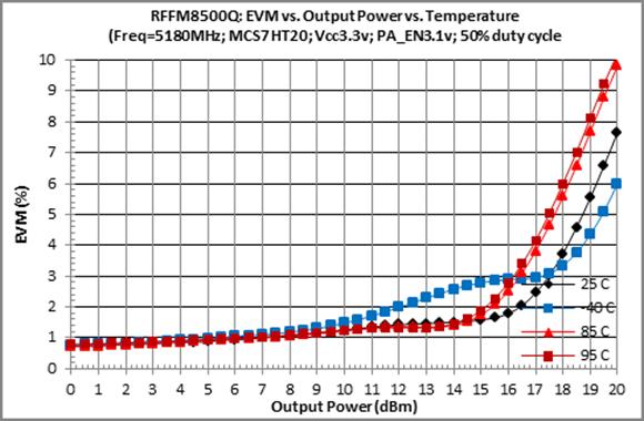

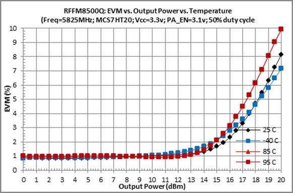
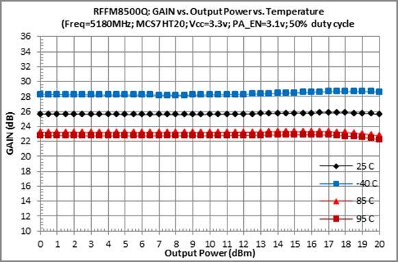
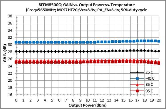
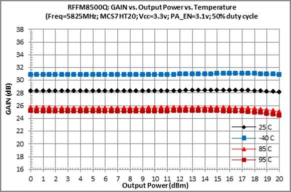
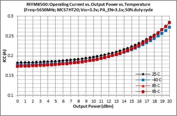
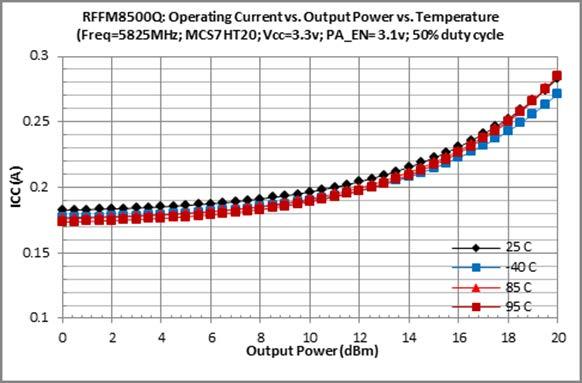
5 Performance Plots application circuitry and specifications at any time without prior notice. 5 of 10

6 application circuitry and specifications at any time without prior notice. 6 of 10
7 Applications Schematic LNA_EN C_RX ANT RX VCC 1uF Vdd 0.1uF NC / NC Pdet PA_EN TX application circuitry and specifications at any time without prior notice. 7 of 10
8 Pin Out ANT C_RX LNA_EN RX 2 11 VCC 3 10 VCC VDD 4 9 N/C TX N/C PA_EN Pdet Package Drawing application circuitry and specifications at any time without prior notice. 8 of 10
9 PCB Patterns Notes: 1. Shaded area represents Pin 1 location. 2. Thermal vias for center slug C should be incorporated into the PCB design. The number and size of thermal vias will depend on the application, power dissipation and electrical requirements. Example of the number and size of vias can be found on the RFMD evaluation board layout (gerber files are available upon request) application circuitry and specifications at any time without prior notice. 9 of 10
10 Pin Names and Descriptions Pin Name Description 1 Ground connection. 2 RX RF output port for the a/n LNA. Input is matched to 50Ω and DC block is provided. 3 Ground connection. 4 VDD Supply voltage for the LNA. See applications schematic for biasing and bypassing components. 5 PDET Power detector voltage for TX section. P DET voltage varies with output power. May need external capacitor for noise decoupling. 6 PA_EN Control voltage for the PA and TX switch. See Logic Control Table for proper settings. 7 NC Not connected. 8 TX RF input port for the a/n PA. Input is matched to 50Ω and DC block is provided. 9 NC Not connected. 10 VCC Supply voltage for the PA. See applications schematic for biasing and bypassing components. 11 VCC Supply voltage for the PA. See applications schematic for biasing and bypassing components. 12 Ground connection. 13 ANT RF bidirectional antenna port matched to 50Ω and is DC blocked internally. 14 Ground connection. 15 C_RX Receive switch control pin. See Logic Control Table for proper level. 16 LNA_EN Control voltage for the LNA. See Logic Control Table for proper settings. Pkg Base Ground connection. application circuitry and specifications at any time without prior notice. 10 of 10
RFFM V to 5.0V, 2.4GHz to 2.5GHz b/g/n/ac WiFi Front End Module. Features. Applications. Ordering Information
 3.0V to 5.0V, 2.4GHz to 2.5GHz 802.11b/g/n/ac WiFi Front End Module The RFFM4293 provides a complete integrated solution in a single front end module (FEM) for WiFi 802.11b/g/n/ac and Bluetooth systems.
RFFM8511TR7. 4.9GHz to 5.85GHz a/n/ac WiFi Front End Module. Features. Applications. Ordering Information
 4.9GHz to 5.85GHz 802.11a/n/ac WiFi Front End Module The provides a complete integrated solution in a single front end module (FEM) for WiFi 802.11a/n/ac systems. The ultra-small factor and integrated
RFFM4503TR7. Features. Applications. Ordering Information. Package: Laminate, 16-pin, 3.0mm x 3.0mm x 1.0mm
 RFFM4503 4.9GHz to 5.85GHz 802.11a/n/ac Wi-Fi Front End Module The RFFM4503 provides a complete integrated solution in a single front end module (FEM) for Wi-Fi 802.11a/n/ac systems. The ultrasmall factor
RFFM3482Q 2.4GHz to 2.5GHz, Automotive WiFi Front End Module
 2.4GHz to 2.5GHz, Automotive WiFi Front End Module Package Style: QFN, 16-pin, 3mm x 3mm x 0.45mm RXBN RXBP GND ANT 16 15 14 13 Features Single Voltage Supply 3.3V to 4.2V Integrated 2.5GHz b/g/n Amplifier,
RFFM V to 4.0V, 450MHz to 470MHz Transmit/Receive Front End Module
 .V to.0v, 0MHz to 0MHz Transmit/Receive Front End Module Package Style: LGA, 8-Pin,.mm x.0mm NC 8 Features Tx Output Power: 0dBm Tx Gain: 0dB Separate 0Ω Tx/Rx Transceiver Interface Rx Insertion Loss:
RFPA V 2.4GHz to 2.5GHz Matched Power Amplifier
 5.0V 2.4GHz to 2.5GHz Matched Power Amplifier Package: Laminate, 14-pin,7mm x 7mm x 1mm VCC 1 14 VCC3 PA_EN 2 13 Features P OUT = 29dBm; EVM = 3%; 11n MCS7 HT40 Input and Output Matched to 50Ω High Gain:
RFFM V to 4.2V, ISM Band, 1W, 405MHz to 475MHz Transmit/Receive Module. Features. Applications. Ordering Information
 RFFM6403 2.5V to 4.2V, ISM Band, 1W, 405MHz to 475MHz Transmit/Receive Module The RFFM6403 is a single-chip front end module (FEM) for applications in the 405MHz and 475MHz ISM Bands. The RFFM6403 addresses
RF V to 4.2V, 2.4GHz Front End Module
 3.0V to 4.2V, 2.4GHz Front End Module Package Style: QFN, 20-Pin, 3.5mm x 3.5mm x 0.5mm TXCT _BAIS GND NC 15 14 13 12 11 Features TX Output Power: 23dBm TX Gain: 28dB RX Gain: 11.5dB RX NF: 3dB Integrated
RF V TO 3.6V, 2.4GHz FRONT END MODULE
 3.V TO 3.6V, 2.4GHz FRONT END MODULE Package Style: QFN, 2-Pin, 3.mmx3.mmx.mm NC VBAT VBAT NC 4 3 2 Features Tx Output Power=22dBm Integrated RF Front End Module with TX/RX switch, PA, filter, and DP2T
RFFM MHz Transmit/Receive Module
 925MHz Transmit/Receive Module This module is intended for 868MHz and 915MHz AMR solutions. The FEM provides separate ports for Rx/Tx paths, single-ended Tx and single-ended Rx or Rx differential port,
RF V TO 4.2V, 2.4GHz FRONT END MODULE
 3.V TO 4.2V, 2.4GHz FRONT END MODULE Package Style: QFN, 2-Pin, 3.5mmx3.5mmx.5mm TXCT GND VCC_BAIS VCC NC 15 14 13 12 11 Features TX Output Power: 22dBm RX Gain: 11.5dB RX NF: 2.5dB Integrated RF Front
RFPA V to 5.0V, 2.4GHz to 2.5GHz Integrated PA Module
 Preliminary RFPA52.V to 5.V, 2.GHz to 2.5GHz Integrated PA Module Package: Laminate, mm x mm x mm RFIN Input Bias Match Circuit PA_EN Features P OUT = 2dBm, 5V < % Dynamic EVM db Typical Gain High PAE
LNA VCC RX OUT TX IN VREG. Product Description. Ordering Information. Standard 25 piece bag Standard 2500 piece reel. GaAs HBT GaAs MESFET InGaP HBT
 2.4GHz TO 2.5GHz, 802.11b/g/n SINGLE-BAND FRONT END MODULE Package Style: QFN, 16-pin, 3.0 x 3.0 x 0.5 mm LNA EN C RX C TX BT 16 15 14 13 Features Single Module Radio Front- End Single Supply Voltage 3.0V
RF V TO 4.0V, 915MHz TRANSMIT/RECEIVE MODULE
 RF6693.1V to 4.V, 91MHz Transmit/Receive Module RF669 3.1V TO 4.V, 91MHz TRANSMIT/RECEIVE MODULE Package: LGA, 28-Pin,.mm x.mm ASW_RX BAL_IN 1 28 27 26 2 24 23 22 Features Tx Output Power: 3dBm NC 2 3
GND GND RFN BALUN RFP GND. Product Description. Ordering Information. Standard 2500 piece reel. GaAs HBT GaAs MESFET InGaP HBT
 RFFM0.0V TO.V,.GHZ FRONT END MODULE Package Style: Laminate, -Pin, mm x mm x mm C_RX_TX VCCLNA N/C ANTSEL 0 9 CE 8 Features Tx Output Power=dBm Integrated RF Front End Module with Balun, PA, filter, LNA
RF3241SR. RF3241 Quad-Band GSM, Polar EDGE Transmit Module, Six UMTS TRX Switch Ports
 Quad-Band GSM, Polar EDGE Transmit Module, Six UMTS TRX Switch Ports The RF3241 is a quad-band GSM/GPRS, Polar EDGE transmit module with six interchangeable RF switch ports. The power amplifier supports
LNA In. Input Match. LNA Vref. LNA Sel. RX Switch. TX Switch GND. PA Vcc2 GND GND. PA Out. Product Description. GaAs HBT GaAs MESFET InGaP HBT
 3.0V to 4.2V, ISM Band Transmit/Receive Module with Diversity Transfer Switch RFFM6904 3.0V TO 4.2V, ISM BAND TRANSMIT/RECEIVE MODULE WITH DIVERSITY TRANSFER SWITCH Package: LGA, 32-pin, 8mm x 8mm x 1.2mm
QPF4200SR. Wi-Fi Front End Module. Product Overview. Key Features. Functional Block Diagram. Applications. Ordering Information
 Product Overview The Qorvo QPF4200 is an integrated front end module (FEM) designed for Wi-Fi 802.11ax systems. The compact form factor and integrated matching minimizes layout area in the application.
915MHz Transmit/Receive Module
 RF6599 915MHz Transmit/Receive Module This module is intended for 915MHz AMR solutions. It provides separate ports for Rx and Tx paths and two ports on the output for connecting a diversity solution or
RFVC GHz to 12.1GHz MMIC VCO with Fo/2 and Fo/4 Outputs
 10.8GHz to 12.1GHz MMIC VCO with Fo/2 and Fo/4 Outputs RFMD's RFVC1844 is a 5V InGaP MMIC VCO with an integrated frequency divider providing additional Fo/2 and Fo/4 outputs. With an Fo frequency range
RFVC1843TR7. 9.8GHz to 11.3GHz MMIC VCO with Fo/2 and Fo/4 Outputs. Features. Applications. Ordering Information
 RFVC1843 9.8GHz to 11.3GHz MMIC VCO with Fo/2 and Fo/4 Outputs RFMD's RFVC1843 is a 5V InGaP MMIC VCO with an integrated frequency divider providing additional Fo/2 and Fo/4 outputs. With an Fo frequency
QPF4206BTR7. Wi-Fi Front End Module. Product Overview. Key Features. Functional Block Diagram. Applications. Ordering Information PRELIMINARY
 Product Overview The Qorvo is an integrated front end module (FEM) designed for Wi-Fi 802.11ax systems. The compact form factor and integrated matching minimizes layout area in the application. Performance
RFSW6062 Low Insertion High Isolation SP6T Switch 5MHz to 6000MHz
 Low Insertion High Isolation SP6T Switch 5MHz to 6000MHz The RFSW6062 is a low loss, high isolation SP6T switch with performance optimized for use in Cellular BTS applications. Plus it is also ideally
RF2436 TRANSMIT/RECEIVE SWITCH
 Transmit/Receive Switch RF2436 TRANSMIT/RECEIVE SWITCH Package Style: SOT-5 Features Single Positive Power Supply Low Current Consumption db Insertion Loss at 900MHz 24dB Crosstalk Isolation at 900MHz
RF V TO 4.2V, 2.4GHz FRONT-END MODULE
 3.0V TO 4.2V, 2.4GHz FRONT-END MODULE Package Style: QFN, 20-Pin, 3.5mmx3.5mmx0.5mm Features TX Output Power: 22dBm TX Gain: 28dB RX Gain: 11.5dB RX NF: 2.5dB Integrated LNA With Bypass Mode Applications
RFVC1800 Wideband MMIC VCO with Buffer Amplifier 8GHz to 12GHz
 Wideband MMIC VCO with Buffer Amplifier 8GHz to 12GHz RFMD s wideband voltage controlled oscillator is a GaAs InGaP HBT MMIC with integrated VCO core and RF output buffer. The part operates from a single
RF V, SWITCH AND LNA FRONT END SOLUTION
 3.3V, SWITCH AND LNA FRONT END SOLUTION Package Style: QFN, -pin, 2mmx2mmx0.5mm C_BT 9 BT GND 7 Features Single Supply Voltage 3.0V to.5v Integrated SP3T Switch and LNA With Bypass Typical gain is db and
RFFM8216TR7-5K. 2.4 GHz Integrated Wi-Fi Front-End Module
 RFFM8216 2.4 GHz Integrated Wi-Fi Front-End Module Product Overview The RFFM8216 provides a complete integrated solution in a single front end module (FEM) for WiFi 802.11b/g/n/ac systems.performance is
RF V TO 4.5V, 915MHZ ISM BAND TRANSMIT/RECEIVE MODULE
 4.0V to 4.5V, 915MHz ISM AND TRANS- MIT/REEIVE MODULE 4.0V TO 4.5V, 915MHZ ISM AND TRANSMIT/REEIVE MODULE Package: LGA, 28-pin, 6mm x 6mm DAV1 N PAV2 1 28 27 26 25 24 23 22 Features Tx Output Power: 28dm
SGL0363Z. 5MHz to 2000MHz Low Noise Amplifier. Germanium. Simplified Device Schematic. Vpc. Narrow-band Matching Network. Gnd
 5MHz to MHz Low Noise Amplifier Silicon Germanium 5MHz to MHz LOW NOISE AMPLIFIER SILICON GERMANIUM Package: SOT-363 Product Description RFMD s is a low power, low noise amplifier. It is designed for.7v
RFSA3043TR7. 75Ω Voltage Controlled Attenuator 5MHz to 3000MHz. Features. Applications. Ordering Information RFSA3043
 75Ω Voltage Controlled Attenuator 5MHz to 3000MHz RFMD s RFSA3043 is a fully monolithic analog voltage controlled attenuator (VCA) featuring exceptional linearity over a typical temperature compensated
RF5623 SINGLE 5.0V, 3.3 TO 3.8 GHZ LINEAR POWER AMPLIFIER
 Single 5.0V, 3.3 to 3.8 GHz Linear Power Amplifier SINGLE 5.0V, 3.3 TO 3.8 GHZ LINEAR POWER AMPLIFIER Package Style: QFN, 16-Pin, 3mmx3mmx0.45mm Features High Gain; 32dB 2.5% EVM (RMS) at 26dBm, 5.0V Integrated
AND0281. AND b/g/n/ac Power Amplifier, LNA and Tx/Rx/BT Switch PRELIMINARY DATA SHEET - Rev 1.2
 FEATURES Supports 802.11ac high-data rate standard Fully integrated FEIC including 2 GHz Power Amplifier, Low Noise Amplifier with Bypass mode and SP3T TX/RX/BT Switch 1.8% Dynamic EVM @ POUT = +18 dbm
RF V, 2.4GHz TO 2.7GHz HIGH POWER AMPLIFIER
 5.0V, 2.4GHz to 2.7GHz High Power Amplifier RF5652 5.0V, 2.4GHz TO 2.7GHz HIGH POWER AMPLIFIER Package: QFN, 32-Pin, 5mmx5mmx0.85mm 32 31 30 29 28 27 26 VBIAS VCC1 VCC2 25 1 24 Features High Gain = 34dB
SAW BPF SW2_OUT GND GND 868/915 RFIO SW2 GND 450 RFIO GND CTL1 CTL2 CTL LOGIC CTL3 CTL4 CTL5 VDIG. Product Description. Ordering Information
 2.7V to 4.4V, 9MHz Transmit/Receive Module; Thru Mode 4MHz to 928MHz RF6549 2.7V to 4.4V, 9MHz Transmit/Receive Module; Thru Mode 4MHz to 928MHz Package: LGA, 32-Pin, 6mm x 6mm TX TX SAW BPF SAW BPF SW2_OUT
RFPA GHz TO 5.9GHz 2W InGaP AMPLIFIER
 4.9GHz to 5.9GHz 2W InGaP AMPLI- FIER RFPA5026 4.9GHz TO 5.9GHz 2W InGaP AMPLIFIER Package: DFN, 6-pin, 5.59mm x 6.23mm x 0.85mm Vcc Features P1dB=33dBm at 5V 802.11g 54Mb/s Class AB Performance P OUT
AWL a/n/ac Power Amplifier, LNA and Tx/Rx Switch DATA SHEET - Rev 2.0
 FEATURES Supports emerging 802.11ac high-data rate standard Fully integrated FEIC including 5GHz Power Amplifier, Low Noise Amplifier with Bypass mode and SP2T TX/RX Switch
RFX8425: 2.4 GHz CMOS WLAN/Bluetooth Dual-Mode RFeIC with PA, LNA, and SP3T
 DATA SHEET RFX8425: 2.4 GHz CMOS WLAN/Bluetooth Dual-Mode RFeIC with PA, LNA, and SP3T Applications Smartphones, feature phones. and MIDs with WLAN/Bluetooth WLAN/Bluetooth platforms requiring shared antenna
RF V TO 5.0V, 3.3GHz TO 3.8GHz LINEAR POWER AMPLIFIER
 3.0V to 5.0V, 3.3GHz to 3.8GHz Linear Power Amplifier RF5603 3.0V TO 5.0V, 3.3GHz TO 3.8GHz LINEAR POWER AMPLIFIER Package Style: QFN, 16-Pin, 3mmx3mmx0.45mm Features High Gain; 32dB 2.5% EVM (RMS) at
Not For New Design FMS W GaAs phemt SPDT SWITCH. Product Description. Features. Applications
 10W GaAs phemt SPDT Switch FMS2031-001 10W GaAs phemt SPDT SWITCH Package: 3 mm x 3 mm QFN Product Description The FMS2031-001 is a 10 W, Single-pole, Double-throw, (SPDT) GaAs phemt reflective antenna
DATA GND VCC GND RF1 GND GND GND. Product Description. Ordering Information. Sample bag with 25 pieces 7 Sample reel with 100 pieces
 Serial Controlled 75W Digital Step Attenuator 5MHz to 2000MHz, 6- Bit, LSB SERIAL CONTROLLED 75 DIGITAL STEP ATTENUATOR 5MHz TO 2000MHz, 6-BIT, Package: MCM, 24-Pin, 4.2mm x 4.2mm Features Frequency Range
RF V TO 4.0V,915MHz Transmit/Receive
 3.3V to 4.0V,9MHz Transmit/Receive Module RF639 3.3V TO 4.0V,9MHz Transmit/Receive Module Package: LGA, 8-Pin,.mm x.0mm Features Tx Output Power: dbm Separate 0 Tx/Rx Transceiver Interface Rx Insertion
RF5633 SINGLE 5.0V, 3.3 TO 3.8GHZ LINEAR POWER AMPLIFIER
 Single 5.0V, 3.3 to 3.8GHz Linear Power Amplifier RF5633 SINGLE 5.0V, 3.3 TO 3.8GHZ LINEAR POWER AMPLIFIER Package Style: QFN, 24-Pin, 4 mm x 4 mm x 0.9 mm Features High Gain; 34dB Supports Low Gain Mode
CMOS 5GHz WLAN ac RFeIC WITH PA, LNA AND SPDT
 CMOS 5GHz WLAN 802.11ac RFeIC WITH PA, LNA AND SPDT RX LEN 16 RXEN ANT 15 14 13 12 11 Description RFX8051 is a highly integrated, single-chip, single-die RFeIC (RF Front-end Integrated Circuit) which incorporates
2.4GHZ CMOS WLAN / BT DUAL-MODE RFEIC WITH PA, LNA & SP3T
 2.4GHZ CMOS WLAN / BT DUAL-MODE RFEIC WITH PA, LNA & SP3T ANT DESCRIPTION DET VMODE 1 2 3 16 15 14 13 12 11 10 RFX8425 is a pure CMOS-based, single-chip/single-die RFeIC (RF Front-end Integrated Circuit)
VC1. Input Match RF IN. Product Description. Ordering Information. Standard 25 piece bag Standard 2500 piece reel. GaAs HBT GaAs MESFET InGaP HBT
 3.3V, 5GHz LINEAR POWER AMPLIFIER Package Style: QFN, 8-Pin, 2.2mmx2.2mmx0.45mm Features Single Supply Voltage 3.0V to 5.0V No external matching components 28dB Typical Gain Across Band P OUT =17dBm@
RF5632 SINGLE 5.0V, 2.3 TO 2.7 GHZ LINEAR POWER AMPLIFIER
 Single 5.0V, 2.3 to 2.7 GHz Linear Power Amplifier RF5632 SINGLE 5.0V, 2.3 TO 2.7 GHZ LINEAR POWER AMPLIFIER Package Style: QFN, 24-Pin, 4mmx4mmx0.9mm VBIAS VC1 24 23 22 21 20 VC2 19 Features 34dB Small
RF8889A SP10T ANTENNA SWITCH MODULE
 SP10T ANTENNA SWITCH MOD- ULE RF8889A SP10T ANTENNA SWITCH MODULE Package: QFN, 3.0mmx3.8mmx0.85mm GSM Rx1 RF8889A GSM Rx2 Features Broadband Performance Suitable for all Cellular Modulation Schemes up
SZM-5066Z 5.0V, 5GHz HIGH POWER LINEAR POWER AMPLIFIER
 5.0V, 5GHz HIGH POWER LINEAR POWER AMPLIFIER Package Style: QFN, 40-Pin, 6mm x 6mm Features Single Supply Voltage 5.0V 8dB Typical Gain Across Band P OUT = 25dBm
RFGA0024. InGaP HBT. 1000MHz. Product Description. Ordering Information
 InGaP HBT MMIC Amplifier 5MHz TO 1MHz RFGA24 InGaP HBT MMIC Amplifier 5MHz TO 1MHz Package: SOT-89 Features Low Cost Broadband Gain Internally Matched Internal Active Bias No Dropping Resistor Single Supply
Absolute Maximum Ratings Parameter Rating Unit Max Input Power, OFDM Modulated, 3:1 Load VSWR +39 dbm Max Input Power, 2:1 VSWR +41 dbm ESD HBM Rating
 1W GaAs phemt SPDT Switch FMS231-1 1W GaAs phemt SPDT SWITCH Package: 3mmx3mm QFN Product Description The FMS231-1 is a 1W, Single-pole, Double-throw, (SPDT) GaAs phemt reflective antenna switch. The switch
QPL7210TR7. 2.4GHz Wi-Fi LNA+BAW Receive Module. Product Overview. Key Features. Functional Block Diagram. Applications. Ordering Information
 2.4GHz Wi-Fi LNA+BAW Receive Module Product Overview The provides a complete integrated receive solution in a single placement front end module (FEM) for Wi-Fi 802.11a/n/ac systems. The full integration
RFDA4005TR13. 6-Bit, Digital Controlled Variable Gain Amplifier 50MHz to 4000MHz
 6-Bit, Digital Controlled Variable Gain Amplifier 50MHz to 4000MHz RFMD s RFDA4005 is a digitally controlled variable gain amplifier featuring high linearity over the entire gain control range with noise
SDA-3000 GaAs Distributed Amplifier
 GaAs Distributed Amplifier RFMD s SDA-3000 is a directly coupled (DC) GaAs microwave monolithic integrated circuit (MMIC) driver amplifier die designed for use as a Mach Zehnder Modulated (MZM) laser driver
Vbias GND GND. Input Match TXIN GND. Pdown. Product Description. Ordering Information. GaAs HBT GaAs MESFET InGaP HBT
 3.3V to 5.0V, 2.4GHz TO 2.5GHz HIGH POWER FRONT END MODULE RFFM4200 3.3V TO 5.0V, 2.4GHz TO 2.5GHz HIGH POWER FRONT END MODULE Package: 6mm x 6mm Laminate Vcc1 Vcc2 Vcc3 Features 34d Typical Gain cross
VCC RF IN. Input Match VREG. Product Description. Ordering Information. Standard 25 piece bag Standard 2500 piece reel. GaAs HBT GaAs MESFET InGaP HBT
 3.0V TO 3.6V, 2.4GHz TO 2.5GHz LINEAR POWER AMPLIFIER Package Style: QFN, 8-Pin, 2.2x2.2x0.45mm Features Single Power Supply 3.0V to 3.6V 30dB Typical Gain, Input ed to 50 2.4GHz to 2.5GHz Frequency Range
CMOS 5GHz WLAN ac RFeIC WITH PA, LNA AND SPDT
 CMOS 5GHz WLAN 802.11ac RFeIC WITH PA, LNA AND SPDT RX LEN 16 RXEN ANT 15 14 13 12 11 Description RFX8051B is a highly integrated, single-chip, single-die RFeIC (RF Front-end Integrated Circuit) which
SGA2363ZDC to 5000MHz, Cascadable. SiGe HBT. MMIC Amplifier. Frequency (GHz) 5000 MHz >10dB
 5000 MHz >10dB") DC to 5MHz, Cascadable SiGe HBT MMIC Amplifier SGA233Z DC to 5MHz, CASCADABLE SiGe HBT MMIC AMPLIFIER Package: SOT-33 Product Description The SGA233Z is a high performance SiGe HBT MMIC Amplifier. A Darlington
DC to 5MHz, Cascadable SiGe HBT MMIC Amplifier SGA233Z DC to 5MHz, CASCADABLE SiGe HBT MMIC AMPLIFIER Package: SOT-33 Product Description The SGA233Z is a high performance SiGe HBT MMIC Amplifier. A Darlington
Product Description. Ordering Information. GaAs MESFET Si BiCMOS
 Digital Controlled Variable Gain Amplifier 1700MHz to 2400MHz RFDA2077 DIGITAL CONTROLLED VARIABLE GAIN AMPLIFIER 1700MHz to 2400MHz Package: MCM 32-Pin, 7.0mmx7.0mm Features Dual Channel VGA Frequency
RFX8053: CMOS 5 GHz WLAN ac RFeIC with PA, LNA, and SPDT
 DATA SHEET RFX8053: CMOS 5 GHz WLAN 802.11ac RFeIC with PA, LNA, and SPDT Applications 802.11a/n/ac WiFi devices Smartphones Tablets/MIDs Gaming Consumer electronics Notebooks/netbooks/ultrabooks Mobile/portable
CMOS 2.4GHZ ZIGBEE/ISM TRANSMIT/RECEIVE RFeIC
 CMOS 2.4GHZ ZIGBEE/ISM TRANSMIT/RECEIVE RFeIC Description 17 1 2 3 4 TXRX VDD VDD D 16 15 14 13 12 11 10 ANT 9 The is a fully integrated, single-chip, single-die RFeIC (RF Front-end Integrated Circuit)
RFX8050: CMOS 5 GHz WLAN ac RFeIC with PA, LNA, and SPDT
 DATA SHEET RFX8050: CMOS 5 GHz WLAN 802.11ac RFeIC with PA, LNA, and SPDT Applications 802.11a/n/ac Smartphones LEN RXEN ANT Tablets/MIDs Gaming Notebook/netbook/ultrabooks Mobile/portable devices RX Consumer
RF3376 General Purpose Amplifier
 General Purpose Amplifier RF3376 General Purpose Amplifier Package Style: SOT8 Features DC to >6000MHz Operation Internally Matched Input and Output 22dB Small Signal Gain +2.0dB Noise Figure +11dBm Output
CMOS 2.4GHZ TRANSMIT/RECEIVE WLAN RFeIC
 CMOS 2.4GHZ TRANSMIT/RECEIVE WLAN RFeIC 17 1 RX 2 3 VDD VDD DNC 16 15 14 13 12 11 10 ANT Description The RFX2402C is a fully integrated, single-chip, single-die RFeIC (RF Front-end Integrated Circuit)
CMOS 5GHz WLAN a/n/ac RFeIC WITH PA, LNA, AND SPDT
 CMOS 5GHz WLAN 802.11a/n/ac RFeIC WITH PA, LNA, AND SPDT Description RX 1 2 LNA_EN 16 ANT 15 14 13 12 11 RFX8055 is a highly integrated, single-chip, single-die RFeIC (RF Front-end Integrated Circuit)
Gain and Return Loss vs Frequency. s22. Frequency (GHz)
") SBA4086Z DCto5GHz, CASCADABLE InGaP/GaAs HBT MMIC AMPLIFIER Package: SOT-86 Product Description RFMD s SBA4086Z is a high performance InGaP/GaAs Heterojunction Bipolar Transistor MMIC Amplifier. A Darlington
SBA4086Z DCto5GHz, CASCADABLE InGaP/GaAs HBT MMIC AMPLIFIER Package: SOT-86 Product Description RFMD s SBA4086Z is a high performance InGaP/GaAs Heterojunction Bipolar Transistor MMIC Amplifier. A Darlington
Simplified Device Schematic. Pin 18. Pin 8. Pin 16. Stage 1 Bias. Stage 2 Bias. Pin 10
 7MHz to 2.7GHz 5V 1W Power Amplifier SZA-244(Z) 7MHz to 2.7GHz 5V 1W Power Amplifier Package: QFN, 4mm x 4mm Product Description RFMD s SZA-244 is a high efficiency class AB heterojunction bipolar transistor
RF V TO 4.0V, 470MHz to 510MHz TRANSMIT/RECEIVE MODULE
 3.3V to 4.0V, 470MHz to 510MHz Transmit/Receive Module 3.3V TO 4.0V, 470MHz to 510MHz TRNSMIT/REEIVE MODULE Package: LG, 8-Pin, 5.5mm x 5.0mm VReg V 1 8 7 6 5 4 3 Features Tx Output Power: 30dm Separate
RF1136 BROADBAND LOW POWER SP3T SWITCH
 BROADBAND LOW POWER SP3T SWITCH Package Style: QFN, 12-Pin, 2.5 mm x 2.5 mm x 0.6 mm Features Low Frequency - 3.5 GHz Operations Very Low Insertion Loss: Cell Band 0.25 db PCS Band 0.30 db High Isolation:
CMOS 2.4GHZ ZIGBEE/ISM TRANSMIT/RECEIVE RFeIC
 hot RFX2401C CMOS 2.4GHZ ZIGBEE/ISM TRANSMIT/RECEIVE RFeIC Description 1 2 3 4 TXRX 17 VDD VDD DNC 16 15 14 13 12 11 10 ANT 9 The RFX2401C is a fully integrated, single-chip, single-die RFeIC (RF Front-end
RFPA3805TR13. GaAs HBT 2-Stage Power Amplifier 700MHz to 2700MHz
 GaAs HBT 2-Stage Power Amplifier 700MHz to 2700MHz RFMD s RFPA3805 is a GaAs HBT linear power amplifier specifically designed for Wireless Infrastructure applications. Using a highly reliable GaAs HBT
RF1 RF2 RF3 RF4. Product Description. Ordering Information. GaAs MESFET Si BiCMOS Si CMOS
 BROADBAND HIGH POWER SP4T SWITCH Package Style: QFN, 12-pin, 2.5mmx2.5mm Features 2kV HBM ESD Protection on All Ports Low Frequency to >2.7GHz Operation Low Insertion Loss: 0.4dB at 1GHz Very High Isolation:
N/C GND LOIN GND N/C N/C N/C N/C. VLOA1 VLOA2 N/C N/C Vc1 Vc2 Vg2 VMPA. Product Description. Ordering Information
 RFUV173 RFUV173 21GHz TO 26.GHz GaAs MMIC IQ UPCONVERTER Package: QFN, 32-Pin, mm x mm x.9mm N/C GND I N/C GND Q N/C Vg1 32 31 3 29 28 27 26 2 Features RF Frequency: 21GHz to 26.GHz LO Frequency (LSB):
SGA3363Z. = 35 ma (Typ.) Frequency (GHz) T L MHz >10dB 255 C/W
 Frequency (GHz) T L MHz >10dB 255 C/W") SGA3363Z DC to MHz, CASCADABLE SiGe HBT MMIC AMPLIFIER Package: SOT-363 Product Description The SGA3363Z is a high performance SiGe HBT MMIC Amplifier. A Darlington configuration featuring one-micron emitters
SGA3363Z DC to MHz, CASCADABLE SiGe HBT MMIC AMPLIFIER Package: SOT-363 Product Description The SGA3363Z is a high performance SiGe HBT MMIC Amplifier. A Darlington configuration featuring one-micron emitters
Product Description. Ordering Information. GaAs HBT GaAs MESFET InGaP HBT
 RECEIVE AGC AMPLIFIER Package Style: MSOP-8 Features Supports Basestation Applications -55dB to +51dB Gain Control Range at 85MHz Single 3V Power Supply IN+ 1 IN- 2 GND 3 8 VCC1 7 VCC2 6 OUT+ -2dBm Input
RDA1005L DIGITAL CONTROLLED VARIABLE GAIN AMPLIFIER 50 MHZ TO 4000 MHZ, 6 BIT
 Digital Controlled Variable Gain Amplifier 50 MHz to 4000 MHz, 6 Bit RDA1005L DIGITAL CONTROLLED VARIABLE GAIN AMPLIFIER 50 MHZ TO 4000 MHZ, 6 BIT Package: MCM, 32-Pin, 5.2 mm x 5.2 mm Features Broadband
Absolute Maximum Ratings Parameter Rating Unit V D1, V D2, V D3 +8 V V G 0 V Junction Temperature C Continuous P DISS (T = ) C/W (derate 37 mw/ C abov
 C/W (derate 37 mw/ C abov") 9.8GHz to 13.5GHz High Linearity RFPA1002 9.8GHz TO 13.5GHz HIGH LINEARITY POWER AMPLIFIER Package: Ceramic QFN, -pin, 6mm x 6mm x 0.95mm 38 Vd1 Vg2 Vd2a 37 36 34 33 1 Features Frequency Range: 9.8GHz
9.8GHz to 13.5GHz High Linearity RFPA1002 9.8GHz TO 13.5GHz HIGH LINEARITY POWER AMPLIFIER Package: Ceramic QFN, -pin, 6mm x 6mm x 0.95mm 38 Vd1 Vg2 Vd2a 37 36 34 33 1 Features Frequency Range: 9.8GHz
VCC1 GND IN GND LOP LON GND GND. Product Description. GaAs HBT GaAs MESFET InGaP HBT
 Direct Quadrature Modulator 145MHz to 27MHz RFMD214 DIRECT QUADRATURE MODULATOR 145MHz TO 27MHz Package: QFN, 24-Pin, 4mm x 4mm VCC1 IN IP 24 23 22 21 2 19 Features ACPR Performance: -7dBc Typ. for 1-Carrier
RFPA TO 5 V PROGRAMMABLE GAIN HIGH EFFICIENCY POWER AMPLIFIER
 3 TO 5 V PROGRAMMABLE GAIN HIGH EFFICIENCY POWER AMPLIFIER Package Style: QFN, 16-Pin, 3 mm x 3 mm Features 0.5 W CW Output Power at 3.6 V 1 W CW Output Power at 5 V 32 db Small Signal Gain at 900 MHz
SGA2463Z. Frequency (GHz) 18.0 dbm 1950MHz. 7.2 dbm 1950 MHz 255 C/W
 18.0 dbm 1950MHz. 7.2 dbm 1950 MHz 255 C/W") SGA243Z DC to 5MHz, CASCADABLE SiGe HBT MMIC AMPLIFIER Package: SOT-33 Product Description The SGA243Z is a high performance SiGe HBT MMIC Amplifier. A Darlington configuration featuring one-micron emitters
SGA243Z DC to 5MHz, CASCADABLE SiGe HBT MMIC AMPLIFIER Package: SOT-33 Product Description The SGA243Z is a high performance SiGe HBT MMIC Amplifier. A Darlington configuration featuring one-micron emitters
CMOS 2.4GHZ ZIGBEE/ISM TRANSMIT/RECEIVE RFeIC
 CMOS 2.4GHZ ZIGBEE/ISM TRANSMIT/RECEIVE RFeIC Description 17 1 2 3 4 TXRX VDD VDD D 16 15 14 13 12 11 10 ANT 9 The RFX2401C is a fully integrated, single-chip, single-die RFeIC (RF Front-end Integrated
RF V, 2.4GHz TO 2.5GHz HIGH POWER FRONT END MODULE
 V, 2.4GHz TO GHz HIGH POWER FRONT END MODULE V, 2.4GHz TO GHz HIGH POWER FRONT END MODULE Package: 6mmx6mm Laminate Vcc1 Vcc2 Vcc3 Features 35d Typical Gain cross Frequency and P OUT =27.5dm
NLB-310. Cascadable Broadband GaAs MMIC Amplifier DC to 10GHz
 Cascadable Broadband GaAs MMIC Amplifier DC to 10GHz NLB-310 The NLB-310 cascadable broadband InGaP/GaAs MMIC amplifier is a low-cost, high-performance solution for general purpose RF and microwave amplification
RF3826TR13. 9W GaN Wide-Band Power Amplifier 30MHz to 2500MHz. Features. Applications. Ordering Information RF3826
 9W GaN Wide-Band Power Amplifier 30MHz to 2500MHz The RF3826 is a wideband Power Amplifier designed for CW and pulsed applications such as wireless infrastructure, RADAR, two way radios, and general purpose
RFDA3016 Digital Controlled Variable Gain Amplifier 3000MHz to 3800MHz, 6-Bit 0.5dB LSB Control
 Digital Controlled Variable Gain Amplifier 3MHz to 38MHz, 6- Bit.dB LSB Control RFDA316 Digital Controlled Variable Gain Amplifier 3MHz to 38MHz, 6-Bit.dB LSB Control Package: MCM 28-Pin, 6.mm x 6.mm 28
RF1226 BROADBAND MEDIUM POWER DIFFERENTIAL SPDT SWITCH
 BROADBAND MEDIUM POWER DIFFERENTIAL SPDT SWITCH Package Style: QFN, 12-pin, 2.0 mm x 2.0 mm x 0.55 mm Features Broadband Performance Low Frequency to 3.5 GHz Very Low Insertion Loss 0.25 db Typ at 0.90
RF3375 GENERAL PURPOSE AMPLIFIER
 Basestation Applications Broadband, Low-Noise Gain Blocks IF or RF Buffer Amplifiers Driver Stage for Power Amplifiers Final PA for Low-Power Applications High Reliability Applications RF3375General Purpose
SBB MHz to 6000MHz InGaP HBT ACTIVE BIAS GAIN BLOCK. Features. Product Description. Applications
 50 to 6000 InGaP HBT Active Bias Gain Block SBB3000 50 to 6000 InGaP HBT ACTIVE BIAS GAIN BLOCK Package: Bare Die Product Description RFMD s SBB3000 is a high performance InGaP HBT MMIC amplifier utilizing
RFSW1012SR. Broadband SPDT Switch. Product Overview. Key Features. Functional Block Diagram. Ordering Information
 Product Overview The is a single-pole double-throw (SPDT) switch designed for applications requiring very low insertion loss and high power handling capability. The excellent linearity performance of the
RFDA0035 DIGITAL CONTROLLED IF DUAL VGA 5 BIT 1dB LSB CONTROL
 Digital Controlled IF Dual VGA RFDA0035 DIGITAL CONTROLLED IF DUAL VGA 5 BIT 1dB LSB CONTROL Package: QFN 32-Pin, 5.0mmx5.0mm 32 31 29 OPB- A1 A0 IPA+ IPA- GNDA VCCA OPA+ OPA- 28 27 26 25 Features Dual
2.4 GHz Front-End Module SST12LF01
 FEATURES: Gain: Typically 12 db gain across 2.4 2.5 GHz for Receiver (RX) chain. Typically 29 db gain across 2.4 2.5 GHz over temperature C to +8 C for Transmitter (TX) chain. Low-Noise Figure Typical
RF V LOW NOISE AMPLIFIER/ 3V DRIVER AMPLIFIER
 3.3V LOW NOISE AMPLIFIER/ 3V DRIVER AMPLIFIER Package Style: SOT 5-Lead Features Low Noise and High Intercept Point Adjustable Bias Current Power Down Control Single 2.7V to 5.0V Power Supply 0.4GHz to
GHz RF Front-End Module. o C
 Functional Block Diagram Features 4 High Efficient Power Amplifier: 41% at Pout= 23dBm -PA P-1dB: +21dBM Typical @ +3.3V-PA Low Noise Amplifier (NF typical 1.8dB)-LNA Low Insertion Loss:0.4dB@ 2.45GHz-Switch
GND GND GND. Product Description. Ordering Information. Sample bag with 25 pieces 7 Sample reel with 100 pieces. GaAs MESFET Si BiCMOS Si CMOS Si BJT
 Temperature Compensating Attenuator TEMPERATURE COMPENSATING ATTENUATOR Package: QFN, 16-Pin,.9mm x 3mm x 3mm GND VDD GND GND 16 15 14 13 Features Patent Pending Circuit Architecture Broadband 5MHz to
RFVA1017 ANALOG CONTROLLED VARIABLE GAIN AMPLIFIER
 Analog Controlled Variable Gain Amplifier RFVA1017 ANALOG CONTROLLED VARIABLE GAIN AMPLIFIER Package: MCM, 7mm x 7mm VCTRL 8 Features 1425MHz to 1550MHz Operation Gain = 27dB Typical Gain Adjustment Range
CGA-6618Z Dual CATV 5MHz to 1000MHz High Linearity GaAs HBT Amplifier CGA-6618Z DUAL CATV 5MHz to 1000MHz HIGH LINEARITY GaAs HBT AMPLIFIER Package: E
 Dual CATV 5MHz to 1MHz High Linearity GaAs HBT Amplifier DUAL CATV 5MHz to 1MHz HIGH LINEARITY GaAs HBT AMPLIFIER Package: ESOP- Product Description RFMD s CGA-1Z is a high performance GaAs HBT MMIC amplifier.
RF3857 DUAL CHANNEL LNA WITH BYPASS MODE
 DUAL CHANNEL LNA WITH BYPASS MODE Package Style: QFN, 16-Pin, 3mmx3mmx0.45mm Features Low Noise and High Intercept Point Adjustable Bias Current Power Down Low Insertion Loss Bypass Feature 1.8V to 4V
RF7234 3V TD-SCDMA/W-CDMA LINEAR PA MODULE BAND 1 AND 1880MHz TO 2025MHz
 3V TD-SCDMA/W-CDMA LINEAR PA MODULE BAND 1 AND 1880MHz TO 2025MHz Package Style: Module, 10-Pin, 3mmx3mmx1.0mm Features TD-SCDMA and HSDPA Compliant Low Voltage Positive Bias Supply (3.4V to 4.2V) +28dBm
Product Description. Ordering Information. GaAs HBT GaAs MESFET InGaP HBT
 GPS Low Noise Amplifier with Integrated Input/Output SAW Filters RF2818 GPS LOW NOISE AMPLIFIER WITH INTEGRATED INPUT/OUTPUT SAW FILTERS Package: Module, 3.0mmx2.5mmx1.0mm Features Compact Footprint: 3.0mmx2.5mmx1.0mm
2.4 GHz TX / RX Booster With Diversity Switch for IoT / BLE / ZigBee
 2.4 GHz TX / RX Booster With Diversity Switch for IoT / BLE / ZigBee NC DNC NC TXRX 21 1 2 3 4 5 VDD VDD 20 19 18 DNC DNC 17 16 6 7 8 9 TXEN RXEN PDET Mode 10 SWant 15 IND 14 ANTA 13 12 ANTB 11 DESCRIPTION