RFID Anti-Collision System Using the Spread Spectrum Technique
|
|
|
- Ezra Hall
- 5 years ago
- Views:
Transcription
1 Using the Spread Spectrum Technique Document ID: PG-TR AR Date: 26 April 2005 Anil Rohatgi 777 Atlantic Ave. Atlanta GA Voice: (404) Fax: (404) No portion of this document may be copied or reproduced without written ( ) consent of the Georgia Institute of Technology
2 Using the Spread Spectrum Technique By: Anil Rohatgi Supervisor: Prof. Gregory D. Durgin Georgia Institute of Technology Propagation Group 4/26/
3 Introduction The abbreviation RFID stands for Radio Frequency Identification, and is a technology that is vastly and rapidly advancing. An RFID system creates a situation where any product can be labeled with essentially any information, and the owner can access this information at any time without having direct contact with the item. The immediate and most prominent goal of RFID is to allow the owner of the system to keep track of his inventory without manually having to handle each individual item. There are also numerous other applications that can be extended for these systems. Essentially, any pertinent information about an item can be stored on the item itself, making automation and control incredibly simple, fast, and noninvasive. The possibilities are endless. The goal of this project was to design and fabricate a fully functional RFID system from scratch. The system was designed to sense and identify 255 mutually exclusive items. The tag was designed to encode a variable identity and transmit this information. On the receiver end, an algorithm was developed in Matlab to process, detect, and decrypt the incoming information to recover the identity of the chip it is currently sensing. How RFID works The basic RFID system consists of two essential parts: the RFID interrogator, and the RFID tag. The purpose of the RFID interrogator is to transmit a set frequency for detection, and then receive this waveform back in a modulated form. The RFID tag is the part that is placed upon the desired item. Inside this tag is where the information and identity of the item is stored. Once the tag senses an incoming waveform, the data logic - 3 -

4 inside the chip modulates the waveform and sends the modulated signal back to the interrogator. The modulated signal is in the form of a bit sequence, inside of which is the desired information and the identity of the item. Figure 1 shows the basic components of an RFID system, and how they interact with each other. Figure 1 Basic RFID components The way the RFID tag modulates and reflects the incoming waveform into a bit sequence is through the use of a diode and the reflection properties of a transmission line. Located between the tag s antenna and the data logic circuits used to control the modulation is a transmission line with a diode attached to the end. When the data logic circuits desire to transmit a bit one, a high voltage is output across the diode, forcing it to act like an open circuit. The reflection coefficient of an open circuit transmission line is one, and all of the incoming waveform is reflected back to the interrogator. However, when the control logic desires to send a bit zero back to the interrogator, it outputs a low voltage across the diode and forces it to look like a short circuit. This short circuit transmission line has a reflection coefficient of zero, and none of the incoming waveform is reflected back. By - 4 -

5 toggling the voltage seen across the diode, the data control logic circuit can effectively transmit any desired bit sequence back to the interrogator. Anti-Collision The system described above works effectively if there is only a single tag in the sensing environment; however, problems arise when multiple objects modulate and reflect the incoming signal. The ability for the receiver to identify which item it is receiving information from in the presence of multiple responses is known as Anti-Collision. The method implemented in the proposed system is known as Spread Spectrum technology. How Spread Spectrum Works: The theory behind using the Spread Spectrum exclusion process is as follows. The data that is to be transmitted is multiplied by a pseudo random sequence. Each tag contains a unique sequence. The bit rate of the pseudorandom sequence is much higher than the bit rate of the data. The output of this multiplication (high frequency) is then used to toggle the diode, and a high bit rate waveform is sent back to the interrogator. Figure 2 shows this process and the result. Figure 2. Tag combination process - 5 -

6 On the interrogator side, what it sees is a combination of multiple high frequency waves arriving at the same time. In order to recover the information, the receiver must have a way to process the data. The key to this recovery process lies within the unique pseudorandom sequence that was combined with the data from the desired tag. If the interrogator knows the pseudorandom sequence associated with the desired tag information, it can recover the data. To do this, theoretically all that needs to be done is to multiply the incoming signal by the same pseudorandom sequence that is combined with the desired data. Assuming the incoming waveform is centered on zero and has peaks that range from negative one to positive one, doing this operation would force the modulating sequence to converge to one for the desired wave, thus only leaving behind the low frequency data wave. When this unique pseudorandom sequence is multiplied with the other waves comprising the incoming waveform received by the interrogator, other high frequency waves are created. Therefore the only low frequency wave left behind is the desired original data. Figure 3 demonstrates the recombination process. Figure 3. Recombination process - 6 -
7 Once the multiplication is completed, the original data can be recovered by passing the resulting waveform through a low pass filter. All the high frequency waves generated from other tags will be removed. System Tag Design The system that was implemented was designed to generate 255 unique pseudorandom sequences based on a variable phase shift located on the tag. This phase shift is where the identity of the tag will be encoded. Two 8-bit shift registers were connected in a feedback sequence in order to generate their maximum length pseudo random sequence of 255 bits. These two sequences were then combined through an XOR gate, and the resulting output is used as the modulating high frequency signal for the data. Figure 4 shows the circuit diagram for these two pseudorandom sequence generators. Figure 4. Schematic for the two PN generators - 7 -

8 The phase shift, in bits, between the two pseudorandom sequences before they are combined, determines the identity of the tag. Thus, there are 255 possible phase shifts between the signals before the sequences begin to repeat, and thus there are 255 possible tags that can be implemented using this schematic. Figure 5 shows the two pseudorandom sequences with no phase shift between them. Figure 6, shows the same two sequences delayed apart by 241 ticks. Figure 5. Two PN sequences with 241 bit delay Figure 6. Two PN sequences with no delay. The phase shift was accomplished by delaying the clock signal fed into the second shift register. A counter was employed as a mechanism for timing the number of bits needed to delay the clock signal sent to the second generator. The value loaded initially into the counter, determines how many ticks the counter will wait before allowing the second shift register to begin, and therefore how many bits the signal will be delayed by. This initial value is established using a set of dipswitches, and can be changed to mimic any of the 255 possible tags. The numeric identity of the tag is thus encoded and related to initial counter value by the equation: tag ID number = 255 initial counter value Equation
9 In order to keep the counter for resetting itself every time it rolled over and consequently restarting the delay sequence, the outputs of the counter were fed through a series of AND gates set to trigger once the number 254 had been reached. On the next clock tick, the output of the AND gates will be high. This value was fed directly into the count enable input of the counter forcing the counter to freeze at 255. The output of the AND gates was also inverted and used to AND together with the original clock signal being fed into the second shift register. This ensured that the clock signal would remain zero until the counter had reached its end value of 255. Once this number has been attained, output of the AND gates is one, and the original clock signal is allowed to pass into the second shift register. Figures 7 and 8 show the original clock signal and the second clock signal with a delay. In Figure 7, the delay and ID number of the tag is three, and in figure 8 the delay and ID number is Figure 7. Clock signal delayed by 3 bits Figure 8. Clock signal delayed by 252 bits The schematic of the phase delay circuit is shown in figure 9 A full schematic of the entire tag circuit can be found as an appendix to the report

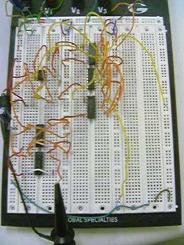
10 Figure 8. Phase delay circuit System Tag Hardware The tag created for this system was built on a proto board. The chips were powered by a 5 Volt power supply, and drew a current of.02amps. The overall power consumption of the entire tag came out to be 0.1Watts. The chips laid out on the board consisted of two 8- bit shift registers, one 555D timer chip, two 4 bit counters, two quad AND gate chips, one inverter chip, one XOR gate chip, one 8 bit dip switch, and 5 toggle switches. A picture of the board lay out is included in Figure 9. The dip switches in the bottom of the board are where the initial conditions for the counter are set. The set of toggle switches on the right side of the board are used when the ID of the tag is changed. In order to reset the tag ID, first set the dip switches to the desired ID by using the inverse of equation 1. Then set all the switches to the upward position in order starting from the bottom switch to the top switch. Once the top switch is flipped, the clock is stopped. Next, flip all the switches back downward starting again from the bottom switch. Once the top switch has been flipped downward, the chip has
11 been reset, and is transmitting the new ID. A larger version of figure 9 can be found in the appendix. Figure 9. Tag Hardware layout System Interrogator Design The design for the interrogator for the RFID system consisted of multiple parts. The transmission and receiver antennas were two copper prefabricated horn and rectangular waveguides. There were to be placed next to each other, in order to use their similar radiation patters to essentially narrow the direction of transmission and reception by nullifying the noise of the adjacent antenna. The transmission antenna was to be attached to a function generator that would output a sine wave of 915 MHz, the frequency
12 commonly associated with UHF RFID. This wave is what irradiates the tag, and what gets modulated and reflected by the tag. The receiving antenna would be attached to a spectrum analyzer that would be set to monitor the peaks at frequencies near 915MHz. If the system is functioning correctly, the peaks should rise and fall according to the data being reflected from the tag. This data would then be run through a threshold chip, most likely a Schmitt trigger, and then logged into a computer through a data acquisition board. From here, the recovery of the tag s identification would take place in Matlab. Matlab Data Processing: Once the bit sequence being received from the interrogator has been logged and recovered, an algorithm was written in Matlab in order to simulate all the possible combinations of pseudorandom sequences that could be output by the tag, and compare them to the incoming sequence. Because there are 255 possible phase shift combinations that can generate the output pseudorandom sequence of the tag, there needed to be 255 simulated sequences to compare with the input data stream. Once a match has been found, the computer logs the phase shift used in the simulation, and returns this number as the ID of the tag. However, there is still another problem because the interrogator cannot tell when the sequence begins and when it ends. Although sampling 255 bits of the incoming waveform ensures that the entire sequence is captured, it does not ensure what bit the sequence begins and ends with. Thus if directly compared to the identical simulated
13 sequence, their phase differences would cause the comparison to give a false negative result. Thus, in order to ensure the correct tag ID, each simulated sequence needed to be bit shifted 255 times, and each time compared to the input data. Thus the total number of iterations for a 255 tag system turned out to be 65,025. The code for a rough implementation of this algorithm is included as an appendix. Data Extension The system described above is only designed to transmit the ID of a tag to the receiver, and not actual data. The tag built only contains chips to generate the pseudorandom sequence, but there is no data to mix it with. This system can easily be changed to include data, by simply multiplying the output pseudorandom sequence with a lower frequency data stream, and using the result to modulate the diode. However, in the implementation used for this demonstration, the pseudorandom sequence drove the modulating diode directly. On the receiver end of the system, in order to be extended to include data, much more of the data processing would have to be done in real time, in order to perform low pass filtering to recover the data. The same algorithm can be used, but the condition for match would be different. Instead of looking for a matching bit to bit correspondence between a simulated sequence and the input data stream, the algorithm would look for the presence of a low frequency waveform. This would be the data in the tag, and the phase shift that generated the pseudorandom sequence that caused the low frequency waveform to appear is the ID of the tag
14 Conclusions Radio Frequency Identification is a technology with the potential to change the world. More and more people are getting involved in this industry, and it is on the verge of flourishing. Major companies such as Wal-Mart are setting deadlines and mandates to switch their entire inventory to an RFID system in the near future. However, this fledgling technology is not yet developed to the point of a mass scale distribution. Problems involving anti-collision, read range and penetration depth have prevented RFID from hitting the market in a big way. But for every problem, there are numerous engineers working in the background to solve them. The design that was proposed and developed for this project solves the anticollision problem for up to 255 tags located in the sensing environment. Each part in the system was designed, developed and independently tested. However, due to time constraints, the components were never fully integrated together and tested as a whole unit. The scope of this project seemed too ambitious for a one semester time frame. Future work may include system integration and miniaturization of the components. Although the system was never fully implemented, the results from the testing are enough to show proof of concept
15 Appendix 1: Complete Circuit Diagram
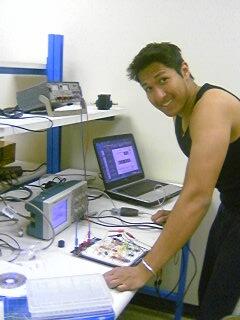
16 Appendix 2: Real Circuit Picture
17 Appendix 3: Matlab Code %This program takes in an input waveform from a DAQ board %and processes the signal to recover the ID of the chip %the signal was sent from %By Anil Rohatgi load inputtest 5 %inputtest5 is the received signal from the Data Acquisition board pickoff = 5; % finished test data initial1=[ ]; %initializing the chip xor1=0; xor2=0; % generating initial PN sequence for i=1:256 xor1=initial1(8); %selecting pickoff points xor2=initial1(pickoff); out(i)=initial1(8); for j=1:7 %shifting index=abs(9-j); initial1(index)=initial1(index-1); end if(xor1==xor2) %XOR initial1(1)=0; else initial1(1)=1; end end plot(out) % phase shift and summation modulated=out; %initializing the second signal that will be modulated answer=0; %Phase shift amount that generated input signal = RFID tag for shift=1:256 templast=modulated(256); %saves the original last value in the unshifted array to be assigned to the first one for k=1:255 %shifting the signals before multiplying them together index2=abs(257-k); modulated(index2)=modulated(index2-1); end modulated(1)=templast; %re-assigns the original last value to the first array position to loop the shift combined=modulated.*out; %multiply the original signal with the shifted signal for phase=1:256 %now, shifts the combined signal and compares it to the input signal. templast2=combined(256) ; for l=1:255 index3=abs(257-l); combined(index3)=combined(index3-1); end
18 end combined(1)=templast2; difference = combined-inputtest5; if (difference.*difference ==0) answer = shift end end


19 Appendix 4: Miscellaneous Pictures
Communication with FCC s Office of Engineering Technology Regarding ISM Compliance of Power-Optimized Waveforms
 Communication with FCC s Office of Engineering Technology Regarding ISM Compliance of Power-Optimized Waveforms Document ID: PG-TR-081120-GDD Date: 11 November 2008 Prof. Gregory D. Durgin 777 Atlantic
B.E. SEMESTER III (ELECTRICAL) SUBJECT CODE: X30902 Subject Name: Analog & Digital Electronics
 SUBJECT CODE: X30902 Subject Name: Analog & Digital Electronics") B.E. SEMESTER III (ELECTRICAL) SUBJECT CODE: X30902 Subject Name: Analog & Digital Electronics Sr. No. Date TITLE To From Marks Sign 1 To verify the application of op-amp as an Inverting Amplifier 2 To
B.E. SEMESTER III (ELECTRICAL) SUBJECT CODE: X30902 Subject Name: Analog & Digital Electronics Sr. No. Date TITLE To From Marks Sign 1 To verify the application of op-amp as an Inverting Amplifier 2 To
3.1 There are three basic logic functions from which all circuits can be designed: NOT (invert), OR, and
, OR, and") EE 2449 Experiment 3 Jack Levine and Nancy Warter-Perez, Revised 6/12/17 CALIFORNIA STATE UNIVERSITY LOS ANGELES Department of Electrical and Computer Engineering EE-2449 Digital Logic Lab EXPERIMENT 3
EE 2449 Experiment 3 Jack Levine and Nancy Warter-Perez, Revised 6/12/17 CALIFORNIA STATE UNIVERSITY LOS ANGELES Department of Electrical and Computer Engineering EE-2449 Digital Logic Lab EXPERIMENT 3
Computer-Based Project in VLSI Design Co 3/7
 Computer-Based Project in VLSI Design Co 3/7 As outlined in an earlier section, the target design represents a Manchester encoder/decoder. It comprises the following elements: A ring oscillator module,
HIGH LOW Astable multivibrators HIGH LOW 1:1
 1. Multivibrators A multivibrator circuit oscillates between a HIGH state and a LOW state producing a continuous output. Astable multivibrators generally have an even 50% duty cycle, that is that 50% of
Simulation Study for the Decoding of UHF RFID Signals
 PIERS ONLINE, VOL. 3, NO. 7, 2007 955 Simulation Study for the Decoding of UHF RFID Signals Shengli Wang 1, Shan Qiao 1,2, Shaoyuan Zheng 1, Zhiguang Fan 1 Jiangtao Huangfu 1, and Lixin Ran 1 1 Department
4/30/2012. General Class Element 3 Course Presentation. Practical Circuits. Practical Circuits. Subelement G7. 2 Exam Questions, 2 Groups
 General Class Element 3 Course Presentation ti ELEMENT 3 SUB ELEMENTS General Licensing Class Subelement G7 2 Exam Questions, 2 Groups G1 Commission s Rules G2 Operating Procedures G3 Radio Wave Propagation
Design and Implementation of FPGA Based Digital Base Band Processor for RFID Reader
 Indian Journal of Science and Technology, Vol 10(1), DOI: 10.17485/ijst/2017/v10i1/109394, January 2017 ISSN (Print) : 0974-6846 ISSN (Online) : 0974-5645 Design and Implementation of FPGA Based Digital
CHAPTER 2. Instructor: Mr. Abhijit Parmar Course: Mobile Computing and Wireless Communication ( )
") CHAPTER 2 Instructor: Mr. Abhijit Parmar Course: Mobile Computing and Wireless Communication (2170710) Syllabus Chapter-2.4 Spread Spectrum Spread Spectrum SS was developed initially for military and intelligence
CHAPTER 2 Instructor: Mr. Abhijit Parmar Course: Mobile Computing and Wireless Communication (2170710) Syllabus Chapter-2.4 Spread Spectrum Spread Spectrum SS was developed initially for military and intelligence
Radio Frequency Identification
 Radio Frequency Identification Retail item level Radio Frequency Tagging Market size: >1 Trillion die/year (Retail, item tags) Economic impact 5% of sales lost due to not on shelf 5-15% of some items stolen
Schmitt Trigger Inputs, Decoders
 Schmitt Trigger, Decoders Page 1 Schmitt Trigger Inputs, Decoders TTL Switching In this lab we study the switching of TTL devices. To do that we begin with a source that is unusual for logic circuits,
Part A: Spread Spectrum Systems
 1 Telecommunication Systems and Applications (TL - 424) Part A: Spread Spectrum Systems Dr. ir. Muhammad Nasir KHAN Department of Electrical Engineering Swedish College of Engineering and Technology February
CDMA Principle and Measurement
 CDMA Principle and Measurement Concepts of CDMA CDMA Key Technologies CDMA Air Interface CDMA Measurement Basic Agilent Restricted Page 1 Cellular Access Methods Power Time Power Time FDMA Frequency Power
Department of Electronics & Telecommunication Engg. LAB MANUAL. B.Tech V Semester [ ] (Branch: ETE)
![Department of Electronics & Telecommunication Engg. LAB MANUAL. B.Tech V Semester [ ] (Branch: ETE)](/thumbs/86/93078052.jpg "Department of Electronics & Telecommunication Engg. LAB MANUAL. B.Tech V Semester [ ] (Branch: ETE)") Department of Electronics & Telecommunication Engg. LAB MANUAL SUBJECT:-DIGITAL COMMUNICATION SYSTEM [BTEC-501] B.Tech V Semester [2013-14] (Branch: ETE) KCT COLLEGE OF ENGG & TECH., FATEHGARH PUNJAB TECHNICAL
Department of Electronics & Telecommunication Engg. LAB MANUAL SUBJECT:-DIGITAL COMMUNICATION SYSTEM [BTEC-501] B.Tech V Semester [2013-14] (Branch: ETE) KCT COLLEGE OF ENGG & TECH., FATEHGARH PUNJAB TECHNICAL
Preface... iii. Chapter 1: Diodes and Circuits... 1
 Table of Contents Preface... iii Chapter 1: Diodes and Circuits... 1 1.1 Introduction... 1 1.2 Structure of an Atom... 2 1.3 Classification of Solid Materials on the Basis of Conductivity... 2 1.4 Atomic
Exam Booklet. Pulse Circuits
 Exam Booklet Pulse Circuits Pulse Circuits STUDY ASSIGNMENT This booklet contains two examinations for the six lessons entitled Pulse Circuits. The material is intended to provide the last training sought
UMAINE ECE Morse Code ROM and Transmitter at ISM Band Frequency
 UMAINE ECE Morse Code ROM and Transmitter at ISM Band Frequency Jamie E. Reinhold December 15, 2011 Abstract The design, simulation and layout of a UMAINE ECE Morse code Read Only Memory and transmitter
Spread Spectrum Communications and Jamming Prof. Kutty Shajahan M G S Sanyal School of Telecommunications Indian Institute of Technology, Kharagpur
 Spread Spectrum Communications and Jamming Prof. Kutty Shajahan M G S Sanyal School of Telecommunications Indian Institute of Technology, Kharagpur Lecture - 06 Tutorial I Hello friends, welcome to this
COMBINATIONAL and SEQUENTIAL LOGIC CIRCUITS Hardware implementation and software design
 PH-315 COMINATIONAL and SEUENTIAL LOGIC CIRCUITS Hardware implementation and software design A La Rosa I PURPOSE: To familiarize with combinational and sequential logic circuits Combinational circuits
Propagation Group Research at Georgia Tech
 Propagation Group Research at Georgia Tech by Prof. Gregory D. Durgin 17 November 2004 Personal History Where I Came From My Most Influential VT Prof s Prof. David A. de Wolf Undergraduate Study Very mathematical
Definition of RF-ID. Lecture on RF-IDs
 Definition of RF-ID RF-ID: Radio Frequency Identification. Indicates the use of Electromagnetic waves to detect and identify TAGS (i.e. labels) purposely attached to objects Basic components (2) Interrogator
Chlorophyll a/b-chlorophyll a sensor for the Biophysical Oceanographic Sensor Array
 Intern Project Report Chlorophyll a/b-chlorophyll a sensor for the Biophysical Oceanographic Sensor Array Mary Ma Mentor: Zbigniew Kolber August 21 st, 2003 Introduction Photosynthetic organisms found
GCSE (9-1) WJEC Eduqas GCSE (9-1) in ELECTRONICS ACCREDITED BY OFQUAL DESIGNATED BY QUALIFICATIONS WALES SAMPLE ASSESSMENT MATERIALS
 WJEC Eduqas GCSE (9-1) in ELECTRONICS ACCREDITED BY OFQUAL DESIGNATED BY QUALIFICATIONS WALES SAMPLE ASSESSMENT MATERIALS") GCSE (9-1) WJEC Eduqas GCSE (9-1) in ELECTRONICS ACCREDITED BY OFQUAL DESIGNATED BY QUALIFICATIONS WALES SAMPLE ASSESSMENT MATERIALS Teaching from 2017 For award from 2019 GCSE ELECTRONICS Sample Assessment
GCSE (9-1) WJEC Eduqas GCSE (9-1) in ELECTRONICS ACCREDITED BY OFQUAL DESIGNATED BY QUALIFICATIONS WALES SAMPLE ASSESSMENT MATERIALS Teaching from 2017 For award from 2019 GCSE ELECTRONICS Sample Assessment
Module -18 Flip flops
 1 Module -18 Flip flops 1. Introduction 2. Comparison of latches and flip flops. 3. Clock the trigger signal 4. Flip flops 4.1. Level triggered flip flops SR, D and JK flip flops 4.2. Edge triggered flip
Part A: Spread Spectrum Systems
 1 Telecommunication Systems and Applications (TL - 424) Part A: Spread Spectrum Systems Dr. ir. Muhammad Nasir KHAN Department of Electrical Engineering Swedish College of Engineering and Technology March
Lecture 9: Spread Spectrum Modulation Techniques
 Lecture 9: Spread Spectrum Modulation Techniques Spread spectrum (SS) modulation techniques employ a transmission bandwidth which is several orders of magnitude greater than the minimum required bandwidth
An Empirical Study of UHF RFID Performance. Michael Buettner and David Wetherall Presented by Qian (Steve) He CS Prof.
 He CS Prof.") An Empirical Study of UHF RFID Performance Michael Buettner and David Wetherall Presented by Qian (Steve) He CS 577 - Prof. Bob Kinicki Overview Introduction Background Knowledge Methodology and Tools
An Empirical Study of UHF RFID Performance Michael Buettner and David Wetherall Presented by Qian (Steve) He CS 577 - Prof. Bob Kinicki Overview Introduction Background Knowledge Methodology and Tools
Low Power Pulse-Based Communication
 MERIT BIEN 2009 Final Report 1 Low Power Pulse-Based Communication Santiago Bortman and Paresa Modarres Abstract When designing small, autonomous micro-robotic systems, minimizing power consumption by
The figures and the logic used for the MATLAB are given below.
 MATLAB FIGURES & PROGRAM LOGIC: Transmitter: The figures and the logic used for the MATLAB are given below. Binary Data Sequence: For our project we assume that we have the digital binary data stream.
Number system: the system used to count discrete units is called number. Decimal system: the number system that contains 10 distinguished
 Number system: the system used to count discrete units is called number system Decimal system: the number system that contains 10 distinguished symbols that is 0-9 or digits is called decimal system. As
CDMA - QUESTIONS & ANSWERS
 CDMA - QUESTIONS & ANSWERS http://www.tutorialspoint.com/cdma/questions_and_answers.htm Copyright tutorialspoint.com 1. What is CDMA? CDMA stands for Code Division Multiple Access. It is a wireless technology
Operational Description
 Operational Description Wallterminal WT2000 ISO Tagit The Wallterminal WT2000 consists of the two components control unit and reader unit. The control unit is usually mounted in a save area inside the
Design of Adjustable Reconfigurable Wireless Single Core
 IOSR Journal of Electronics and Communication Engineering (IOSR-JECE) e-issn: 2278-2834,p- ISSN: 2278-8735. Volume 6, Issue 2 (May. - Jun. 2013), PP 51-55 Design of Adjustable Reconfigurable Wireless Single
Digital Logic Circuits
 Digital Logic Circuits Let s look at the essential features of digital logic circuits, which are at the heart of digital computers. Learning Objectives Understand the concepts of analog and digital signals
CHAPTER 6 ANALYSIS OF THREE PHASE HYBRID SCHEME WITH VIENNA RECTIFIER USING PV ARRAY AND WIND DRIVEN INDUCTION GENERATORS
 73 CHAPTER 6 ANALYSIS OF THREE PHASE HYBRID SCHEME WITH VIENNA RECTIFIER USING PV ARRAY AND WIND DRIVEN INDUCTION GENERATORS 6.1 INTRODUCTION Hybrid distributed generators are gaining prominence over the
Three-level Code Division Multiplex for Local Area Networks
 Three-level Code Division Multiplex for Local Area Networks Mokhtar M. 1,2, Quinlan T. 1 and Walker S.D. 1 1. University of Essex, U.K. 2. Universiti Pertanian Malaysia, Malaysia Abstract: This paper reports
Wideband Spectral Measurement Using Time-Gated Acquisition Implemented on a User-Programmable FPGA
 Wideband Spectral Measurement Using Time-Gated Acquisition Implemented on a User-Programmable FPGA By Raajit Lall, Abhishek Rao, Sandeep Hari, and Vinay Kumar Spectral measurements for some of the Multiple
Spread Spectrum. Chapter 18. FHSS Frequency Hopping Spread Spectrum DSSS Direct Sequence Spread Spectrum DSSS using CDMA Code Division Multiple Access
 Spread Spectrum Chapter 18 FHSS Frequency Hopping Spread Spectrum DSSS Direct Sequence Spread Spectrum DSSS using CDMA Code Division Multiple Access Single Carrier The traditional way Transmitted signal
CH 4. Air Interface of the IS-95A CDMA System
 CH 4. Air Interface of the IS-95A CDMA System 1 Contents Summary of IS-95A Physical Layer Parameters Forward Link Structure Pilot, Sync, Paging, and Traffic Channels Channel Coding, Interleaving, Data
12 BIT ACCUMULATOR FOR DDS
 12 BIT ACCUMULATOR FOR DDS ECE547 Final Report Aravind Reghu Spring, 2006 1 CONTENTS 1 Introduction 6 1.1 Project Overview 6 1.1.1 How it Works 6 1.2 Objective 8 2 Circuit Design 9 2.1 Design Objective
The SOL-20 Computer s Cassette interface.
 The SOL-20 Computer s Cassette interface. ( H. Holden. Dec. 2018 ) Introduction: The Cassette interface designed by Processor Technology (PT) for their SOL-20 was made to be compatible with the Kansas
Laboratory Manual CS (P) Digital Systems Lab
 Digital Systems Lab") Laboratory Manual CS 09 408 (P) Digital Systems Lab INDEX CYCLE I A. Familiarization of digital ICs and digital IC trainer kit 1 Verification of truth tables B. Study of combinational circuits 2. Verification
Laboratory Manual CS 09 408 (P) Digital Systems Lab INDEX CYCLE I A. Familiarization of digital ICs and digital IC trainer kit 1 Verification of truth tables B. Study of combinational circuits 2. Verification
(i) Determine the admittance parameters of the network of Fig 1 (f) and draw its - equivalent circuit.
 Determine the admittance parameters of the network of Fig 1 (f) and draw its - equivalent circuit.") I.E.S-(Conv.)-1995 ELECTRONICS AND TELECOMMUNICATION ENGINEERING PAPER - I Some useful data: Electron charge: 1.6 10 19 Coulomb Free space permeability: 4 10 7 H/m Free space permittivity: 8.85 pf/m Velocity
I.E.S-(Conv.)-1995 ELECTRONICS AND TELECOMMUNICATION ENGINEERING PAPER - I Some useful data: Electron charge: 1.6 10 19 Coulomb Free space permeability: 4 10 7 H/m Free space permittivity: 8.85 pf/m Velocity
Ultrasonic Positioning System EDA385 Embedded Systems Design Advanced Course
 Ultrasonic Positioning System EDA385 Embedded Systems Design Advanced Course Joakim Arnsby, et04ja@student.lth.se Joakim Baltsén, et05jb4@student.lth.se Simon Nilsson, et05sn9@student.lth.se Erik Osvaldsson,
ENGINEERING TRIPOS PART II A ELECTRICAL AND INFORMATION ENGINEERING TEACHING LABORATORY EXPERIMENT 3B2-B DIGITAL INTEGRATED CIRCUITS
 ENGINEERING TRIPOS PART II A ELECTRICAL AND INFORMATION ENGINEERING TEACHING LABORATORY EXPERIMENT 3B2-B DIGITAL INTEGRATED CIRCUITS OBJECTIVES : 1. To interpret data sheets supplied by the manufacturers
Course Outline Cover Page
 College of Micronesia FSM P.O. Box 159 Kolonia, Pohnpei Course Outline Cover Page Digital Electronics I VEE 135 Course Title Department and Number Course Description: This course provides the students
On Built-In Self-Test for Adders
 On Built-In Self-Test for s Mary D. Pulukuri and Charles E. Stroud Dept. of Electrical and Computer Engineering, Auburn University, Alabama Abstract - We evaluate some previously proposed test approaches
Department of Electronics & Communication Engineering LAB MANUAL SUBJECT: DIGITAL COMMUNICATION LABORATORY [ECE324] (Branch: ECE)
![Department of Electronics & Communication Engineering LAB MANUAL SUBJECT: DIGITAL COMMUNICATION LABORATORY [ECE324] (Branch: ECE)](/thumbs/96/127341232.jpg "Department of Electronics & Communication Engineering LAB MANUAL SUBJECT: DIGITAL COMMUNICATION LABORATORY [ECE324] (Branch: ECE)") Department of Electronics & Communication Engineering LAB MANUAL SUBJECT: DIGITAL COMMUNICATION LABORATORY [ECE324] B.Tech Year 3 rd, Semester - 5 th (Branch: ECE) Version: 01 st August 2018 The LNM Institute
Department of Electronics & Communication Engineering LAB MANUAL SUBJECT: DIGITAL COMMUNICATION LABORATORY [ECE324] B.Tech Year 3 rd, Semester - 5 th (Branch: ECE) Version: 01 st August 2018 The LNM Institute
ENGR-2300 Electronic Instrumentation Quiz 3 Spring Name: Solution Please write you name on each page. Section: 1 or 2
 ENGR-2300 Electronic Instrumentation Quiz 3 Spring 2018 Name: Solution Please write you name on each page Section: 1 or 2 4 Questions Sets, 20 Points Each LMS Portion, 20 Points Question Set 1) Question
2. WIRELESS IN LOCAL LOOP (WILL).
.") undamentals of WLL 1. INTRODUCTION Access Network, the network between local exchange and subscriber, in the Telecom Network accounts for a major portion of resources both in terms of capital and manpower.
undamentals of WLL 1. INTRODUCTION Access Network, the network between local exchange and subscriber, in the Telecom Network accounts for a major portion of resources both in terms of capital and manpower.
logic system Outputs The addition of feedback means that the state of the circuit may change with time; it is sequential. logic system Outputs
 Sequential Logic The combinational logic circuits we ve looked at so far, whether they be simple gates or more complex circuits have clearly separated inputs and outputs. A change in the input produces
ME 365 EXPERIMENT 8 FREQUENCY ANALYSIS
 ME 365 EXPERIMENT 8 FREQUENCY ANALYSIS Objectives: There are two goals in this laboratory exercise. The first is to reinforce the Fourier series analysis you have done in the lecture portion of this course.
Pearson Education Limited Edinburgh Gate Harlow Essex CM20 2JE England and Associated Companies throughout the world
 Pearson Education Limited Edinburgh Gate Harlow Essex CM20 2JE England and Associated Companies throughout the world Visit us on the World Wide Web at: www.pearsoned.co.uk Pearson Education Limited 2014
Width (W): 44 mm. bus connecting and branching terminal External supply --- Inputs: Number: up to 2 (depending on parameterization: channel 1 to 2)
: 44 mm. bus connecting and branching terminal External supply --- Inputs: Number: up to 2 (depending on parameterization: channel 1 to 2)") Product name: Design: 2-channel push button interface UP (flush-mounting type) Item no.: 1118 00 ETS search path: Gira Giersiepen / input / binary input, 2fold / Universal push putton interface 2fold Functional
Product name: Design: 2-channel push button interface UP (flush-mounting type) Item no.: 1118 00 ETS search path: Gira Giersiepen / input / binary input, 2fold / Universal push putton interface 2fold Functional
1. The decimal number 62 is represented in hexadecimal (base 16) and binary (base 2) respectively as
 and binary (base 2) respectively as") BioE 1310 - Review 5 - Digital 1/16/2017 Instructions: On the Answer Sheet, enter your 2-digit ID number (with a leading 0 if needed) in the boxes of the ID section. Fill in the corresponding numbered
BioE 1310 - Review 5 - Digital 1/16/2017 Instructions: On the Answer Sheet, enter your 2-digit ID number (with a leading 0 if needed) in the boxes of the ID section. Fill in the corresponding numbered
Digital Audio Broadcasting Eureka-147. Minimum Requirements for Terrestrial DAB Transmitters
 Digital Audio Broadcasting Eureka-147 Minimum Requirements for Terrestrial DAB Transmitters Prepared by WorldDAB September 2001 - 2 - TABLE OF CONTENTS 1 Scope...3 2 Minimum Functionality...3 2.1 Digital
Spread Spectrum Techniques
 0 Spread Spectrum Techniques Contents 1 1. Overview 2. Pseudonoise Sequences 3. Direct Sequence Spread Spectrum Systems 4. Frequency Hopping Systems 5. Synchronization 6. Applications 2 1. Overview Basic
Digital Video Broadcast Library (DVB)
") Digital Video Broadcast Library (DVB) Conforming to European Telecommunications Standard ETS 300 744 (March 1997) DVB SystemView by ELANIX Copyright 1994-2005, Eagleware Corporation All rights reserved.
Digital Video Broadcast Library (DVB) Conforming to European Telecommunications Standard ETS 300 744 (March 1997) DVB SystemView by ELANIX Copyright 1994-2005, Eagleware Corporation All rights reserved.
CHAPTER 5 NOVEL CARRIER FUNCTION FOR FUNDAMENTAL FORTIFICATION IN VSI
 98 CHAPTER 5 NOVEL CARRIER FUNCTION FOR FUNDAMENTAL FORTIFICATION IN VSI 5.1 INTRODUCTION This chapter deals with the design and development of FPGA based PWM generation with the focus on to improve the
Ultra-Wideband DesignGuide
 Ultra-Wideband DesignGuide January 2007 Notice The information contained in this document is subject to change without notice. Agilent Technologies makes no warranty of any kind with regard to this material,
Microcircuit Electrical Issues
 Microcircuit Electrical Issues Distortion The frequency at which transmitted power has dropped to 50 percent of the injected power is called the "3 db" point and is used to define the bandwidth of the
DS1267 Dual Digital Potentiometer Chip
 Dual Digital Potentiometer Chip www.dalsemi.com FEATURES Ultra-low power consumption, quiet, pumpless design Two digitally controlled, 256-position potentiometers Serial port provides means for setting
Wireless Communication Project : Spread Spectrum. Name: Qin Xiaosong Student ID:
 Wireless Communication Project : Spread Spectrum Name: Qin Xiaosong Student ID: 5100109073 June 23, 2013 Abstract This report has mainly recorded the process of the project of the Wireless Communication.
ETHERNET TESTING SERVICES
 ETHERNET TESTING SERVICES 10BASE-Te Embedded MAU Test Suite Version 1.1 Technical Document Last Updated: June 21, 2012 Ethernet Testing Services 121 Technology Dr., Suite 2 Durham, NH 03824 University
Pseudo Noise Sequence Generation using Elliptic Curve for CDMA and Security Application
 IJIRST International Journal for Innovative Research in Science & Technology Volume 1 Issue 11 April 2015 ISSN (online): 2349-6010 Pseudo Noise Sequence Generation using Elliptic Curve for CDMA and Security
HT9032. Calling Line Identification Receiver. Block Diagram. Features. Applications. General Description
 Calling Line Identification Receiver Features Operating voltage 3.5V~5.5V Bell 202 FSK and V.23 demodulation Ring detection input and output Carrier detection output Power down mode High input sensitivity
Master of Comm. Systems Engineering (Structure C)
") ENGINEERING Master of Comm. DURATION 1.5 YEARS 3 YEARS (Full time) 2.5 YEARS 4 YEARS (Part time) P R O G R A M I N F O Master of Communication System Engineering is a quarter research program where candidates
ENGINEERING Master of Comm. DURATION 1.5 YEARS 3 YEARS (Full time) 2.5 YEARS 4 YEARS (Part time) P R O G R A M I N F O Master of Communication System Engineering is a quarter research program where candidates
ECE 511: FINAL PROJECT REPORT GROUP 7 MSP430 TANK
 ECE 511: FINAL PROJECT REPORT GROUP 7 MSP430 TANK Team Members: Andrew Blanford Matthew Drummond Krishnaveni Das Dheeraj Reddy 1 Abstract: The goal of the project was to build an interactive and mobile
EE 307 Project #1 Whac-A-Mole
 EE 307 Project #1 Whac-A-Mole Performed 10/25/2008 to 11/04/2008 Report finished 11/09/2008 John Tooker Chenxi Liu Abstract: In this project, we made a digital circuit that operates Whac-A-Mole game. Quartus
Design of low-power, high performance flip-flops
 Int. Journal of Applied Sciences and Engineering Research, Vol. 3, Issue 4, 2014 www.ijaser.com 2014 by the authors Licensee IJASER- Under Creative Commons License 3.0 editorial@ijaser.com Research article
Combinational logic: Breadboard adders
 ! ENEE 245: Digital Circuits & Systems Lab Lab 1 Combinational logic: Breadboard adders ENEE 245: Digital Circuits and Systems Laboratory Lab 1 Objectives The objectives of this laboratory are the following:
Digital Electronics Course Objectives
 Digital Electronics Course Objectives In this course, we learning is reported using Standards Referenced Reporting (SRR). SRR seeks to provide students with grades that are consistent, are accurate, and
Chapter 15: Serial Controlled (HF) Radio Support
 Radio Support") 15-1 Chapter 15: Serial Controlled (HF) Radio Support This section describes the controller's interface for serial controlled radios. Most such radios are for the HF bands, but some such as the FT-736
15-1 Chapter 15: Serial Controlled (HF) Radio Support This section describes the controller's interface for serial controlled radios. Most such radios are for the HF bands, but some such as the FT-736
Spec. Instructor: Center
 PDHonline Course E379 (5 PDH) Digital Logic Circuits Volume III Spec ial Logic Circuits Instructor: Lee Layton, P.E 2012 PDH Online PDH Center 5272 Meadow Estatess Drive Fairfax, VA 22030-6658 Phone &
Module 3: Physical Layer
 Module 3: Physical Layer Dr. Associate Professor of Computer Science Jackson State University Jackson, MS 39217 Phone: 601-979-3661 E-mail: natarajan.meghanathan@jsums.edu 1 Topics 3.1 Signal Levels: Baud
Lecture 15 Analysis of Combinational Circuits
 Lecture 15 Analysis of Combinational Circuits Designing Combinational Logic Circuits A logic circuit having 3 inputs, A, B, C will have its output HIGH only when a majority of the inputs are HIGH. Step
WCDMA Basics Chapter 2 OBJECTIVES:
 WCDMA Basics Chapter 2 This chapter is designed to give the students a brief review of the WCDMA basics of the WCDMA Experimental System. This is meant as a review only as the WCDMA basics have already
T325 Summary T305 T325 B BLOCK 3 4 PART III T325. Session 11 Block III Part 3 Access & Modulation. Dr. Saatchi, Seyed Mohsen.
 T305 T325 B BLOCK 3 4 PART III T325 Summary Session 11 Block III Part 3 Access & Modulation [Type Dr. Saatchi, your address] Seyed Mohsen [Type your phone number] [Type your e-mail address] Prepared by:
Preface to the Third Edition. List of Abbreviations
 Contents Preface to the Third Edition List of Abbreviations 1 Introduction 1 1.1 Automatic Identification Systems 2 1.1.1 Barcode Systems 2 1.1.2 Optical Character Recognition 3 1.1.3 Biometric Procedures
Chapter 2 Overview - 1 -
 Chapter 2 Overview Part 1 (last week) Digital Transmission System Frequencies, Spectrum Allocation Radio Propagation and Radio Channels Part 2 (today) Modulation, Coding, Error Correction Part 3 (next
Web-Enabled Speaker and Equalizer Final Project Report December 9, 2016 E155 Josh Lam and Tommy Berrueta
 Web-Enabled Speaker and Equalizer Final Project Report December 9, 2016 E155 Josh Lam and Tommy Berrueta Abstract IoT devices are often hailed as the future of technology, where everything is connected.
CS302 - Digital Logic Design Glossary By
 CS302 - Digital Logic Design Glossary By ABEL : Advanced Boolean Expression Language; a software compiler language for SPLD programming; a type of hardware description language (HDL) Adder : A digital
MAINTENANCE MANUAL AUDIO MATRIX BOARD P29/
 MAINTENANCE MANUAL AUDIO MATRIX BOARD P29/5000056000 TABLE OF CONTENTS Page DESCRIPTION................................................ Front Cover CIRCUIT ANALYSIS.............................................
GCE AS. WJEC Eduqas GCE AS in ELECTRONICS ACCREDITED BY OFQUAL DESIGNATED BY QUALIFICATIONS WALES SAMPLE ASSESSMENT MATERIALS
 GCE AS WJEC Eduqas GCE AS in ELECTRONICS ACCREDITED BY OFQUAL DESIGNATED BY QUALIFICATIONS WALES SAMPLE ASSESSMENT MATERIALS Teaching from 207 For award from 208 AS ELECTRONICS Sample Assessment Materials
RFID. Presented by BESSER ASSOCIATES. Instructor: Al Scott
 RFID Presented by BESSER ASSOCIATES Instructor: Al Scott 1 COURSE OUTLINE Uses of RFID Basic RFID System ISM Frequency Bands Walmart Directive EPC RFID System How RF part of EPC System Works RF antennas
Design and Analysis of Row Bypass Multiplier using various logic Full Adders
 Design and Analysis of Row Bypass Multiplier using various logic Full Adders Dr.R.Naveen 1, S.A.Sivakumar 2, K.U.Abhinaya 3, N.Akilandeeswari 4, S.Anushya 5, M.A.Asuvanti 6 1 Associate Professor, 2 Assistant
INTEGRATED CIRCUITS. For a complete data sheet, please also download:
 INTEGRATED CIRCUITS DATA SHEET For a complete data sheet, please also download: The IC0 74HC/HCT/HCU/HCMOS Logic Family Specifications The IC0 74HC/HCT/HCU/HCMOS Logic Package Information The IC0 74HC/HCT/HCU/HCMOS
Learning Material Ver 1.1
 Data Formatting & Carrier Modulation Transmitter Trainer and Carrier Demodulation & Data Reformatting Receiver Trainer ST2106 & ST2107 Learning Material Ver 1.1 An ISO 9001 : 2000 company 94, Electronic
). The THRESHOLD works in exactly the opposite way; whenever the THRESHOLD input is above 2/3V CC
. The THRESHOLD works in exactly the opposite way; whenever the THRESHOLD input is above 2/3V CC") ENGR 210 Lab 8 RC Oscillators and Measurements Purpose: In the previous lab you measured the exponential response of RC circuits. Typically, the exponential time response of a circuit becomes important
ENGR 210 Lab 8 RC Oscillators and Measurements Purpose: In the previous lab you measured the exponential response of RC circuits. Typically, the exponential time response of a circuit becomes important
TIMA Lab. Research Reports
 ISSN 292-862 TIMA Lab. Research Reports TIMA Laboratory, 46 avenue Félix Viallet, 38 Grenoble France ON-CHIP TESTING OF LINEAR TIME INVARIANT SYSTEMS USING MAXIMUM-LENGTH SEQUENCES Libor Rufer, Emmanuel
TSTE17 System Design, CDIO. General project hints. Behavioral Model. General project hints, cont. Lecture 5. Required documents Modulation, cont.
 TSTE17 System Design, CDIO Lecture 5 1 General project hints 2 Project hints and deadline suggestions Required documents Modulation, cont. Requirement specification Channel coding Design specification
Learning Outcomes. Spiral 2 3. DeMorgan Equivalents NEGATIVE (ACTIVE LO) LOGIC. Negative Logic One hot State Assignment System Design Examples
 LOGIC. Negative Logic One hot State Assignment System Design Examples") 2-3. Learning Outcomes 2-3.2 Spiral 2 3 Negative Logic One hot State Assignment System Design Examples I understand the active low signal convention and how to interface circuits that use both active high
2-3. Learning Outcomes 2-3.2 Spiral 2 3 Negative Logic One hot State Assignment System Design Examples I understand the active low signal convention and how to interface circuits that use both active high
Capacitive Touch Sensing Tone Generator. Corey Cleveland and Eric Ponce
 Capacitive Touch Sensing Tone Generator Corey Cleveland and Eric Ponce Table of Contents Introduction Capacitive Sensing Overview Reference Oscillator Capacitive Grid Phase Detector Signal Transformer
Pulse-Width Modulation (PWM)
") Pulse-Width Modulation (PWM) Modules: Integrate & Dump, Digital Utilities, Wideband True RMS Meter, Tuneable LPF, Audio Oscillator, Multiplier, Utilities, Noise Generator, Speech, Headphones. 0 Pre-Laboratory
Pulse-Width Modulation (PWM) Modules: Integrate & Dump, Digital Utilities, Wideband True RMS Meter, Tuneable LPF, Audio Oscillator, Multiplier, Utilities, Noise Generator, Speech, Headphones. 0 Pre-Laboratory
 I.E.S-(Conv.)-2007 ELECTRONICS AND TELECOMMUNICATION ENGINEERING PAPER - II Time Allowed: 3 hours Maximum Marks : 200 Candidates should attempt Question No. 1 which is compulsory and FOUR more questions
DS1867 Dual Digital Potentiometer with EEPROM
 Dual Digital Potentiometer with EEPROM www.dalsemi.com FEATURES Nonvolatile version of the popular DS1267 Low power consumption, quiet, pumpless design Operates from single 5V or ±5V supplies Two digitally
Smart Antenna ABSTRACT
 Smart Antenna ABSTRACT One of the most rapidly developing areas of communications is Smart Antenna systems. This paper deals with the principle and working of smart antennas and the elegance of their applications
Digital Image Watermarking by Spread Spectrum method
 Digital Image Watermarking by Spread Spectrum method Andreja Samčovi ović Faculty of Transport and Traffic Engineering University of Belgrade, Serbia Belgrade, november 2014. I Spread Spectrum Techniques
Implementing Logic with the Embedded Array
 Implementing Logic with the Embedded Array in FLEX 10K Devices May 2001, ver. 2.1 Product Information Bulletin 21 Introduction Altera s FLEX 10K devices are the first programmable logic devices (PLDs)
Analysis, Design and Implementation of Automotive Breaking System Based on Gold Sequence with Correlation RADAR
 Analysis, Design and Implementation of Automotive Breaking System Based on Gold Sequence with Correlation RADAR Shrikant Kumar 1, Dr. Paresh Rawat 2 Department of Electronics and Communication, TCST Bhopal