Web-Enabled Speaker and Equalizer Final Project Report December 9, 2016 E155 Josh Lam and Tommy Berrueta
|
|
|
- Holly Higgins
- 6 years ago
- Views:
Transcription
1 Web-Enabled Speaker and Equalizer Final Project Report December 9, 2016 E155 Josh Lam and Tommy Berrueta
2 Abstract IoT devices are often hailed as the future of technology, where everything is connected. Our project adds to the growing list of IoT devices: a speaker and equalizer controlled from the internet. A website allows the user to use playback controls, select songs, and modify the equalization of the audio to their personal preference. Commands are sent to a Raspberry Pi which communicates with an FPGA via SPI. The FPGA filters the audio before sending it back to the Pi as an equalizer in the form of a filter bank with 7 FIR bandpass filters. The Pi then outputs PWM audio to a 4th order butterworth filter and then to an amplifier and set of speakers. However, in the actual implementation of the design, the filter bank did not work outside of simulation. Thus, the design was done using a single FIR filter rather than a full filter bank.

3 Introduction In an ever interconnected world, IoT devices look to enable devices previously independent to be able to be communicate and be controlled via the web. In particular for audio applications, IoT control could be hugely beneficial to remotely control speakers at an event or venue. This project describes the development of a web-enabled speaker and equalizer such that users can select songs via a web server and stream them through an equalizer where they are modified and finally output by speakers. A user could control the playback and equalization in real time and make sure the audio sounds as desired. The system is split up into three main partitions: Raspberry Pi, FPGA and external hardware. The Raspberry Pi hosts the web server where users can control the system. The FPGA hosts the hardware equalizer that is controlled by the settings on the web server. Finally, the external hardware consists of an 8x8 LED array to display current equalizer gains, a pair of speakers and a stereo amplifier to raise the level of the audio signals from the Pi to an audible level. Figure 1 shown below displays a top level view of the system architecture and communication between subsystems. Figure 1: Top-level system diagram.
 and a reset line. Out of the Pi, pin 18 was the PWM output.")
4 Schematics Figure 2: Breadboard schematic. Shown above in figure 2 is our final Breadboarded Project. Of note, the LED array is not shown here since it was not completed. Running between the Pi and the FPGA board are 5 signal lines; the four SPI lines (channel enable, serial clock, MISO, and MOSI) and a reset line. Out of the Pi, pin 18 was the PWM output. To convert from PWM into an analog signal, the PWM wave was sent through a 4th order low pass filter in the form of two Butterworth filters with Sallen-Key topology with a cutoff frequency of 15kHz. The operational amplifier used was single-sided since the PWM wave was also single-sided. The output of these filters was wired to the left and right input of the stereo amplifier, with GND being wired to the negative inputs. Finally, the two speakers were wired to the outputs of the amplifier. Raspberry Pi Design There are two main aspects of the code implemented on the Raspberry Pi; the main loop which handles SPI and PWM communication, and the numerous CGI scripts that control the main loop through shared memory. The Pi communicates with the FPGA and sends out audio through its SPI and PWM peripherals. All peripherals are accessed by writing to corresponding registers in the Pi s memory. These are mapped to using mmap. Much of this project s work was based off of EasyPIO.h (reference) which already initializes and sets up may of the Pi s peripherals, including GPIOs, timers and of course PWM and SPI. However, there were some slight modifications made to the script. The following sections detail those changes and how each peripheral is used.
5 1. GPIO: EasyPIO has functions that write to the registers that change the pin modes and also read and write from the pins. 2. SPI: The SPI peripheral is set up by setting the pin modes of pins 8, 9, 10, and 11 to ALT0. The SPI initialization allows the caller to set the SPI frequency and settings, which can be set to default operation by writing the settings bytes to 0. Sending and receiving is done through the SPI s FIFO register, After a value is written to the FIFO buffer, it is sent, and upon completion, the done bit of the Command and Status register is set to PWM: To write to the PWM, pin 18 is set to mode ALT5. EasyPIO.h initializes the PWM peripheral with the maximum frequency of 25MHz. While it was originally planned to write directly to pins 40 and 45, which are connected directly to the audio jack, the Pi apparently does not grant access to them and in fact only pin 18 is allowed PWM functionality. To write to PWM, the PWM s DAT register is written to to determine the duty cycle of the PWM wave. 4. Timer: The Pi has 4 internal timers running off of a 1 MHz clock. EasyPIO.h utilizes these by implementing delay functions on microsecond scales. To send the PWM samples out at the correct audio sampling frequency, these microsecond delays are used to wait for the length of the period of the frequency. This delay being microseconds is not completely accurate, resulting in slightly sped up or slowed down depending on what the delay is. Of note, it also take a non-zero amount of time to run the rest of the loop body, so the timer had to be experimentally tweaked to get the audio speed as close as possible to the actual rate. These delay functions set one of the four system timers to be a microsecond offset from the current timer. Then, once the current timer reaches this value, it will set a corresponding flag in the system timer s command and status register. A while loop would wait for this condition to be reached, freezing the system until it is. Of the four timers, timers 2 and 0 are often used for other processes and are often inconsistent in performance when used for delays. Timers 3 and 1, on the other hand, perform consistently but are prone to failing resulting in the entire program being stuck in an endless loop. The team s best guess for why this is is that the system timer that fails is somehow set to a different value which the current timer never reaches. To counteract this, the delay function was modified to utilize all four system timers, and exit the while loop if any one of the four timers set a flag. In this way, the only way for the system to fail would be if all four timers failed at the same time. After empirical observation this was deemed to happen infrequently, as the code would have to play several songs in succession before finally failing, an extreme edge case.
6 Website and CGI Scripts The website is at the center of the design, comprising of html action buttons that each trigger their own CGI executable scripts. A screenshot of the website is shown below, with descriptions of each button s function following. Each button redirects back to the project s webpage. Figure 3: Screenshot of website. 1. Play Button: The play button s script is where the main loop is written. The core functionality of the main loop is to take an audio sample, send it over SPI, receive a filtered sample, and send it through PWM. The main loop s settings, such as whether to play music or not or what song to play, all depend on bytes in shared memory. Shared memory is a C programming construct that allows different C scripts to communicate with each other by setting aside a block of memory that the scripts can all read and write to. In addition to redirecting back to the webpage, all scripts connect to the shared memory block using shmget. The outline of the shared memory is as follows in table 1 below:
7 Byte number Use 0 Unused 1 Status - MSB[Filter_On/-Off-, X, X, X, song_changed, locked/-open-, going/-stopped-, playing/-paused-]lsb 2 Song Number 3-9 Gains 0 to 6 Table 1: Shared memory mapping. The first byte is the status byte, where each bit represents a different status setting. Upon pressing the play button, the two least significant bits are set to [going playing]. The code then checks the locked/-open- status bit to determine whether to begin the main loop. The locked/-open- bit ensures that only one instance of the main loop is running at any time, as the play button can still be pressed even if a main loop is already running. If no loop is running, the default setting is open, but as soon as a loop begins (play button pressed), the bit is changed to locked, and will not open until the stop or reset button is pressed. Upon each loop iteration, the main code will check the status byte and respond accordingly. If the Filter_On bit is high, the loop will send received filtered audio to PWM. Otherwise it will send the unfiltered samples. If the song_changed bit is high, the loop will update the string holding the title of the song and re-read the wav file from memory to update the audio sample array. When changing the song, the code will also briefly set the reset pin to high to reset the FPGA. The next 4 bits are unused. The going/-stopped- bit and the playing/-pausedare distinct from one another since a paused song retains its previous sample location and the main loop still runs, but if the song is stopped, the previous sample location will not be held and the loop will exit. In the main loop, if a song is paused, the loop will continue to run (status still locked and going), but will not send SPI or PWM. The song number byte is where the current song number is stored and determines what song is playing. Lastly, the next 7 bytes are used to store the gain settings. 2. Pause, Stop and Reset Buttons: The pause, stop and reset buttons affect the status byte of the previously described shared memory segment. The pause button changes the playing/-paused- bit to 0 (paused) if the going bit is high. The stop button changes the 3 least significant status bits to 000 [open stopped paused]. Lastly, the reset button changes the status byte and the song byte to all zeros and sets all the gain bits to sevens. The reset button also briefly writes the reset pin to high to reset the FPGA.
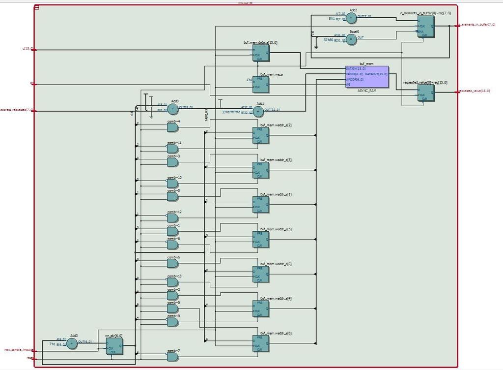
8 3. Song Change Buttons: When one of the song buttons is pressed, it will not only flip the song_changed bit to high, but also change the value stored on this byte corresponding to the song number pressed. Currently, only 12 songs are available to play, but since there is a full byte of information, there could be up to 256 songs without the need for another byte of memory. These songs are stored as wav files in the same folder as the CGI scripts so the executables are able to read them. 4. Filter Toggle Button: The filter on button changes the filter_on bit of the status byte. Specifically it does so by performing an XOR operation to toggle the bit from 1 to 0 or 0 to Gain Buttons: If a plus button is pressed, the gain stored there will be incremented, whereas it will be decremented if a minus button is pressed. The values are capped to be between 0 and 15, with a default value of 7. FPGA Design The FPGA houses the equalizer in the form of a bank of bandpass FIR filters with settable gains. The hardware consists of several submodules all which serve the purpose of streaming and filtering audio through the system. The system takes in audio samples via an SPI module which handles communication between the FPGA and the Raspberry Pi. 16 bit words are sent and received simultaneously as audio is streamed and filtered. In addition to the 16 bit audio sample, a 16 bit sample containing the equalizer gains follows. These two alternating samples are sorted by a finite state machine that sends samples into the FIFO buffer to be accessed by the FIR filters, and the gains to the FIR filters themselves to be used in the calculation. The FIFO buffer is a circular buffer that stores a certain window of samples. This buffer is used to carry out the convolution in the FIR filters. The FIR filter bank consists of a master FIR filter, and 6 slaves. The master filter is the only one that request samples from the FIFO buffer and then passes on those samples to all of the slave filters. This is done such that there only needs to be a single request to the memory at a time. The FIR filter topology itself is a fully pipelined multiply-accumulate architecture. The filter uses a single multiplier running a convolution in a loop between the audio samples and the filter coefficients. The filter coefficients themselves are pre-loaded into memory utilizing a memory initialization file that loads the designed filter into read only memory. The modules are described in more detail in the further sections: 1. SPI: The FPGA s SPI module implements a simple SPI slave that listens for 16-bit words. The module will take MOSI, CS, and SCLK as inputs connected from external pins. It will combine the received bits into 16 bit words and output them as q. It also takes internal input d to be sent
9 out as MISO. Another important logic element is the signal that keeps track of when a full word has been completely received. This done signal goes on to the parsing FSM which routes gains and samples to appropriate subsystems. 2. Parsing FSM: The parsing FSM groups counts every other done signal from the SPI module and sends the equalizer gains onto the FIR filter bank to wait until it gets used, and the audio samples onto the FIFO buffer to fill up the convolution window. 3. FIFO Buffer: The FIFO buffer stores and updates a certain window of input audio samples such that the FIR filters can request samples from the window in order to carry out a convolution. As new samples come in, the values themselves do not move and a pointer instead moves, making all reading and writing relative to the position of said pointer. The FIFO buffer takes in an address requested by the master FIR filter from the bank and will output the requested value. 4. Coefficient Memory: The coefficient memory is a read only memory that is initialized at synthesis with the values of all the coefficients required to design the different FIR filters. There will be as many memories as there are filters given that the coefficients themselves are what define the filters, otherwise they are just convolution modules. These values will be determined ahead of time by designing the filters in MATLAB and converted to the appropriate bit depth. 5. FIR Filter Bank: The FIR filter bank implements 7 FIR filters in parallel that will each carry out a convolution between a buffer of audio samples and the coefficients stored in memory. The resulting signals will be multiplied by the equalizer gains and then added together to create an aggregate filtered signal to be sent back to the Pi via SPI. A master filter will send address requests to the fifo modules and send the samples to the rest in order to avoid issues with communicating with a single memory. However, every filter will communicate with its own coefficient memory since these requests are independent of one another. The received coefficients and samples will be used in a pipelined multiply-accumulate topology to implement the convolution and output the final value to the SPI communication module. 6. LED Array Logic: The LED array logic module would use 16 pins from FPGA to display the equalizer gains as lit bars on the array. In order to display multiple bars simultaneously on the array, time-multiplexing of the pins pulling the LEDs high and low would have to be implemented.
10 However, the LED array was not in the final version of the project and thus was not written in code. Results While a fully integrated deliverable was achieved in the end, our final project did not achieve all deliverables outlined in our project proposal. On the Raspberry Pi side, almost all systems are robustly implemented. The output audio quality is very good considering it is PWM audio, with only a small hiss of noise. The shared memory seamlessly lets different buttons interact with the main loop that plays audio. However, running the main loop for an extended amount of time makes the Pi s microcontroller chip to heat up. Furthermore, the timer peripheral that controls the sample output rate is not absolutely reliable, nor exactly accurate, as there is a possibility of timer failure, and the speed is a best estimation of the correct sample rate. However, the possibility of failure has been observed to be infrequent and the audio sounds close enough to the accurate despite the limitations of the timer peripheral. On the FPGA side, a fully functional FIR filter module was successfully integrated with FIFO and SPI modules. This worked in both simulation and reality. However, in extending the full setup to include a full filter bank with 7 filters each with their own gains, we obtained a working simulation, but the code did not work in reality. The team suspects this was due to timing complications extending from an asynchronous design. Complications that a single FIR filter did not have issues with, but when expanded caused the full FIR filter bank to fail. A timing diagram showing the full FIR bank working in simulation is attached in the appendix. Finally, the 8x8 LED array was not able to be implemented due to time constraints. In total, instead of a web enabled speaker with a 7-bin EQ, our final delivered project was a web-enabled speaker with a toggle-able high pass filter. All Raspberry Pi functionality was achieved as desired and most FPGA functionality was as well. However, while simulation showed the system to function, reality did not prove to be as amenable.
11 Bibliography 1. Butterworth Sallen Key Topology Adafruit Amplifier Usage Shared memory Example Raspberry Pi Peripherals - RM-Peripherals.pdf 5. Digital Design and Computer Architecture Ch EasyPIO.h - Parts List Part Source Vendor Part # Price MCP6002 Op Amp Stereo Amplifier MAX98306 stockroom Adafruit 987 $8.95 (2x) 3 Speakers Adafruit 1314 $3.90 8x8 LED Array Adafruit 455 $3.95

12 Appendix Top Module: SPI Module:

13 FSM: FIFO Buffer:

 * 0x7 (number of")

14 Filter Bank: FIR Filter Filter Bank Simulation Steady State Results: Expected 55 = 0x37 = (0x0ff0 (input) * 0x80 (window size) * 0x7 (number of filters)) >> 16 Given filter tested was a unity gain, and equalizer values were all set to unity.
I hope you have completed Part 2 of the Experiment and is ready for Part 3.
 I hope you have completed Part 2 of the Experiment and is ready for Part 3. In part 3, you are going to use the FPGA to interface with the external world through a DAC and a ADC on the add-on card. You
Lab 1.2 Joystick Interface
 Lab 1.2 Joystick Interface Lab 1.0 + 1.1 PWM Software/Hardware Design (recap) The previous labs in the 1.x series put you through the following progression: Lab 1.0 You learnt some theory behind how one
Lab 3: Embedded Systems
 THE PENNSYLVANIA STATE UNIVERSITY EE 3OOW SECTION 3 FALL 2015 THE DREAM TEAM Lab 3: Embedded Systems William Stranburg, Sean Solley, Sairam Kripasagar Table of Contents Introduction... 3 Rationale... 3
Digital Guitar Effects Box
 Digital Guitar Effects Box Jordan Spillman, Electrical Engineering Project Advisor: Dr. Tony Richardson April 24 th, 2018 Evansville, Indiana Acknowledgements I would like to thank Dr. Richardson for advice
Game Console Design. Final Presentation. Daniel Laws Comp 499 Capstone Project Dec. 11, 2009
 Game Console Design Final Presentation Daniel Laws Comp 499 Capstone Project Dec. 11, 2009 Basic Components of a Game Console Graphics / Video Output Audio Output Human Interface Device (Controller) Game
Lab 2.2 Custom slave programmable interface
 Lab 2.2 Custom slave programmable interface Introduction In the previous labs, you used a system integration tool (Qsys) to create a full FPGA-based system comprised of a processor, on-chip memory, a JTAG
Hello, and welcome to this presentation of the STM32 Digital Filter for Sigma-Delta modulators interface. The features of this interface, which
 Hello, and welcome to this presentation of the STM32 Digital Filter for Sigma-Delta modulators interface. The features of this interface, which behaves like ADC with external analog part and configurable
Roland Kammerer. 13. October 2010
 Peripherals Roland Institute of Computer Engineering Vienna University of Technology 13. October 2010 Overview 1. Analog/Digital Converter (ADC) 2. Pulse Width Modulation (PWM) 3. Serial Peripheral Interface
EE445L Fall 2014 Quiz 2A Page 1 of 5
 EE445L Fall 2014 Quiz 2A Page 1 of 5 Jonathan W. Valvano First: Last: November 21, 2014, 10:00-10:50am. Open book, open notes, calculator (no laptops, phones, devices with screens larger than a TI-89 calculator,
RF4432 wireless transceiver module
 1. Description www.nicerf.com RF4432 RF4432 wireless transceiver module RF4432 adopts Silicon Lab Si4432 RF chip, which is a highly integrated wireless ISM band transceiver. The features of high sensitivity
Arduino Microcontroller Processing for Everyone!: Third Edition / Steven F. Barrett
 Arduino Microcontroller Processing for Everyone!: Third Edition / Steven F. Barrett Anatomy of a Program Programs written for a microcontroller have a fairly repeatable format. Slight variations exist
Embedded Test System. Design and Implementation of Digital to Analog Converter. TEAM BIG HERO 3 John Sopczynski Karim Shik-Khahil Yanzhe Zhao
 Embedded Test System Design and Implementation of Digital to Analog Converter TEAM BIG HERO 3 John Sopczynski Karim Shik-Khahil Yanzhe Zhao EE 300W Section 1 Spring 2015 Big Hero 3 DAC 2 INTRODUCTION (KS)
SPI, Talking to Chips, and Minimizing Noise
 Jonathan Mitchell 996069032 Stark Industries Application Note SPI, Talking to Chips, and Minimizing Noise How do you communicate with a piece of silicon? How do you communicate with a semiconductor. SPI
Figure 1: Functional Block Diagram
 MagAlpha MA750 Key features 8 bit digital and 12 bit PWM output 500 khz refresh rate 7.5 ma supply current Serial interface for data readout and settings QFN16 3x3mm Package General Description The MagAlpha
Hello and welcome to this Renesas Interactive Course that provides an overview of the timers found on RL78 MCUs.
 Hello and welcome to this Renesas Interactive Course that provides an overview of the timers found on RL78 MCUs. 1 The purpose of this course is to provide an introduction to the RL78 timer Architecture.
Ultrasonic Positioning System EDA385 Embedded Systems Design Advanced Course
 Ultrasonic Positioning System EDA385 Embedded Systems Design Advanced Course Joakim Arnsby, et04ja@student.lth.se Joakim Baltsén, et05jb4@student.lth.se Simon Nilsson, et05sn9@student.lth.se Erik Osvaldsson,
EE 307 Project #1 Whac-A-Mole
 EE 307 Project #1 Whac-A-Mole Performed 10/25/2008 to 11/04/2008 Report finished 11/09/2008 John Tooker Chenxi Liu Abstract: In this project, we made a digital circuit that operates Whac-A-Mole game. Quartus
EVDP610 IXDP610 Digital PWM Controller IC Evaluation Board
 IXDP610 Digital PWM Controller IC Evaluation Board General Description The IXDP610 Digital Pulse Width Modulator (DPWM) is a programmable CMOS LSI device, which accepts digital pulse width data from a
Activity 4: Due before the lab during the week of Feb
 Today's Plan Announcements: Lecture Test 2 programming in C Activity 4 Serial interfaces Analog output Driving external loads Motors: dc motors, stepper motors, servos Lecture Test Activity 4: Due before
DS1802 Dual Audio Taper Potentiometer With Pushbutton Control
 www.dalsemi.com FEATURES Ultra-low power consumption Operates from 3V or 5V supplies Two digitally controlled, 65-position potentiometers including mute Logarithmic resistive characteristics (1 db per
Stratix II Filtering Lab
 October 2004, ver. 1.0 Application Note 362 Introduction The filtering reference design provided in the DSP Development Kit, Stratix II Edition, shows you how to use the Altera DSP Builder for system design,
Digital-to-Analog Converter. Lab 3 Final Report
 Digital-to-Analog Converter Lab 3 Final Report The Ion Cannons: Shrinand Aggarwal Cameron Francis Nicholas Polito Section 2 May 1, 2017 1 Table of Contents Introduction..3 Rationale..3 Theory of Operation.3
Solar Mobius Final Report. Team 1821 Members: Advisor. Sponsor
 Senior Design II ECE 4902 Spring 2018 Solar Mobius Final Report Team 1821 Members: James Fisher (CMPE) David Pettibone (EE) George Oppong (EE) Advisor Professor Ali Bazzi Sponsor University of Connecticut
Figure 1: Functional Block Diagram
 MagAlpha MA120 Angular Sensor for 3-Phase Brushless Motor Key features U V W signals for block commutation Adjustable zero 500 khz refresh rate Ultra low latency: 3 µs Serial interface for settings 8.5
Debugging a Boundary-Scan I 2 C Script Test with the BusPro - I and I2C Exerciser Software: A Case Study
 Debugging a Boundary-Scan I 2 C Script Test with the BusPro - I and I2C Exerciser Software: A Case Study Overview When developing and debugging I 2 C based hardware and software, it is extremely helpful
Using Magnetic Sensors for Absolute Position Detection and Feedback. Kevin Claycomb University of Evansville
 Using Magnetic Sensors for Absolute Position Detection and Feedback. Kevin Claycomb University of Evansville Using Magnetic Sensors for Absolute Position Detection and Feedback. Abstract Several types
Brian Hanna Meteor IP 2007 Microcontroller
 MSP430 Overview: The purpose of the microcontroller is to execute a series of commands in a loop while waiting for commands from ground control to do otherwise. While it has not received a command it populates
EE 434 Final Projects Fall 2006
 EE 434 Final Projects Fall 2006 Six projects have been identified. It will be our goal to have approximately an equal number of teams working on each project. You may work individually or in groups of
Serial Communication AS5132 Rotary Magnetic Position Sensor
 Serial Communication AS5132 Rotary Magnetic Position Sensor Stephen Dunn 11/13/2015 The AS5132 is a rotary magnetic position sensor capable of measuring the absolute rotational angle of a magnetic field
ECE 511: FINAL PROJECT REPORT GROUP 7 MSP430 TANK
 ECE 511: FINAL PROJECT REPORT GROUP 7 MSP430 TANK Team Members: Andrew Blanford Matthew Drummond Krishnaveni Das Dheeraj Reddy 1 Abstract: The goal of the project was to build an interactive and mobile
Application Note. Smart LED Dimmer Controlled via Bluetooth AN-CM-225
 Application Note Smart LED Dimmer Controlled via Bluetooth AN-CM-225 Abstract This application note describes how to build a smart digital dimmer using GreenPAK SLG46620V. A dimmer is a common light switch
3-Channel Fun LED Driver
 3-Channel Fun LED Driver Description is a 3-channel fun LED driver which features two-dimensional auto breathing mode. It has One Shot Programming mode and PWM Control mode for RGB lighting effects. The
University of North Carolina-Charlotte Department of Electrical and Computer Engineering ECGR 3157 Electrical Engineering Design II Fall 2013
 Exercise 1: PWM Modulator University of North Carolina-Charlotte Department of Electrical and Computer Engineering ECGR 3157 Electrical Engineering Design II Fall 2013 Lab 3: Power-System Components and
Lock Cracker S. Lust, E. Skjel, R. LeBlanc, C. Kim
 Lock Cracker S. Lust, E. Skjel, R. LeBlanc, C. Kim Abstract - This project utilized Eleven Engineering s XInC2 development board to control several peripheral devices to open a standard 40 digit combination
Catalog
 Catalog 1. Description... - 3-2. Features... - 3-3. Application... - 3-4. Electrical specifications...- 4-5. Schematic... - 4-6. Pin Configuration... - 5-7. Antenna... - 6-8. Mechanical Dimension(Unit:
802.11g Wireless Sensor Network Modules
 RFMProducts are now Murata Products Small Size, Integral Antenna, Light Weight, Low Cost 7.5 µa Sleep Current Supports Battery Operation Timer and Event Triggered Auto-reporting Capability Analog, Digital,
AC Current click PID: MIKROE Weight: 27 g
 AC Current click PID: MIKROE-2523 Weight: 27 g AC Current click can measure alternating currents up to 30A and it features the MCP3201 ADC (analog to digital) converter and the MCP607 CMOS Op Amp, both
RF NiceRF Wireless Technology Co., Ltd. Rev
 - 1 - Catalog 1. Description...- 3-2. Features...- 3-3. Application...- 3-4. Electrical Specifications...- 4-5. Schematic...- 4-6. Pin Configuration...- 5-7. Antenna... - 6-8. Mechanical dimensions(unit:
Rochester Institute of Technology Real Time and Embedded Systems: Project 2a
 Rochester Institute of Technology Real Time and Embedded Systems: Project 2a Overview: Design and implement a STM32 Discovery board program exhibiting multitasking characteristics in simultaneously controlling
DNT2400. Low Cost 2.4 GHz FHSS Transceiver Module with I/O
 2.4 GHz Frequency Hopping Spread Spectrum Transceiver Point-to-point, Point-to-multipoint, Peer-to-peer and Tree-routing Networks Transmitter Power Configurable from 1 to 63 mw RF Data Rate Configurable
EE 314 Spring 2003 Microprocessor Systems
 EE 314 Spring 2003 Microprocessor Systems Laboratory Project #9 Closed Loop Control Overview and Introduction This project will bring together several pieces of software and draw on knowledge gained in
Sound Source Localizer
 Sound Source Localizer Joren Lauwers, Changping Chen Abstract In our final project, we will build a sound source localizer - a system that positions the source of human speech on a 2d map. We will sample
CHAPTER III THE FPGA IMPLEMENTATION OF PULSE WIDTH MODULATION
 34 CHAPTER III THE FPGA IMPLEMENTATION OF PULSE WIDTH MODULATION 3.1 Introduction A number of PWM schemes are used to obtain variable voltage and frequency supply. The Pulse width of PWM pulsevaries with
HOMANN DESIGNS. DigiSpeed. Instruction manual. Version 1.0. Copyright 2004 Homann Designs.
 HOMANN DESIGNS DigiSpeed Instruction manual Version 1.0 Copyright 2004 Homann Designs http://www.homanndesigns.com Table of Contents Introduction...3 Features...3 DigiSpeed Operation Description...5 Overview...5
ELCT 912: Advanced Embedded Systems
 ELCT 912: Advanced Embedded Systems Lecture 5: PIC Peripherals on Chip Dr. Mohamed Abd El Ghany, Department of Electronics and Electrical Engineering The PIC Family: Peripherals Different PICs have different
LM8322 Mobile I/O Companion Supporting Key-Scan, I/O Expansion, PWM, and ACCESS.bus Host Interface
 Mobile I/O Companion Supporting Key-Scan, I/O Expansion, PWM, and ACCESS.bus Host Interface 1.0 General Description The Mobile I/O Companion is a dedicated device to unburden a host processor from scanning
Interactive 1 Player Checkers. Harrison Okun December 9, 2015
 Interactive 1 Player Checkers Harrison Okun December 9, 2015 1 Introduction The goal of our project was to allow a human player to move physical checkers pieces on a board, and play against a computer's
Page 1/10 Digilent Analog Discovery (DAD) Tutorial 6-Aug-15. Figure 2: DAD pin configuration
 Tutorial 6-Aug-15. Figure 2: DAD pin configuration") Page 1/10 Digilent Analog Discovery (DAD) Tutorial 6-Aug-15 INTRODUCTION The Diligent Analog Discovery (DAD) allows you to design and test both analog and digital circuits. It can produce, measure and
Page 1/10 Digilent Analog Discovery (DAD) Tutorial 6-Aug-15 INTRODUCTION The Diligent Analog Discovery (DAD) allows you to design and test both analog and digital circuits. It can produce, measure and
RF4463F30 High Power wireless transceiver module
 RF4463F30 High Power wireless transceiver module 1. Description RF4463F30 adopts Silicon Lab Si4463 RF chip, which is a highly integrated wireless ISM band transceiver chip. Extremely high receive sensitivity
Exercise 3: Sound volume robot
 ETH Course 40-048-00L: Electronics for Physicists II (Digital) 1: Setup uc tools, introduction : Solder SMD Arduino Nano board 3: Build application around ATmega38P 4: Design your own PCB schematic 5:
Pulse-Width Modulation (PWM)
") Pulse-Width Modulation (PWM) Modules: Integrate & Dump, Digital Utilities, Wideband True RMS Meter, Tuneable LPF, Audio Oscillator, Multiplier, Utilities, Noise Generator, Speech, Headphones. 0 Pre-Laboratory
Pulse-Width Modulation (PWM) Modules: Integrate & Dump, Digital Utilities, Wideband True RMS Meter, Tuneable LPF, Audio Oscillator, Multiplier, Utilities, Noise Generator, Speech, Headphones. 0 Pre-Laboratory
Designing with STM32F3x
 Designing with STM32F3x Course Description Designing with STM32F3x is a 3 days ST official course. The course provides all necessary theoretical and practical know-how for start developing platforms based
Application Note. Brushless DC Motor Control AN-1114
 Application Note AN-1114 Abstract In this application note a GreenPAK configuration applicable for a single-phase BLDC motor is introduced. This application note comes complete with design files which
Cyclone II Filtering Lab
 May 2005, ver. 1.0 Application Note 376 Introduction The Cyclone II filtering lab design provided in the DSP Development Kit, Cyclone II Edition, shows you how to use the Altera DSP Builder for system
AN5086 Application note
 Application note I 2 S protocol emulation on STM32L0 Series microcontrollers using a standard SPI peripheral Introduction The I 2 S protocol is widely used to transfer audio data from a microcontroller
EE445L Fall 2014 Quiz 2A Page 1 of 5
 EE445L Fall 2014 Quiz 2A Page 1 of 5 Jonathan W. Valvano First: Last: November 21, 2014, 10:00-10:50am. Open book, open notes, calculator (no laptops, phones, devices with screens larger than a TI-89 calculator,
PSoC and Arduino Calculator
 EGR 322 Microcontrollers PSoC and Arduino Calculator Prepared for: Dr. Foist Christopher Parisi (390281) Ryan Canty (384185) College of Engineering California Baptist University 05/02/12 TABLE OF CONTENTS
A Highly Generalised Automatic Plugin Delay Compensation Solution for Virtual Studio Mixers
 A Highly Generalised Automatic Plugin Delay Compensation Solution for Virtual Studio Mixers Tebello Thejane zyxoas@gmail.com 12 July 2006 Abstract While virtual studio music production software may have
RedPitaya. FPGA memory map
 RedPitaya FPGA memory map Written by Revision Description Version Date Matej Oblak Initial 0.1 08/11/13 Matej Oblak Release1 update 0.2 16/12/13 Matej Oblak ASG - added burst mode ASG - buffer read pointer
SPI Slave to PWM Generation
 April 2011 Introduction Reference Design RD1107 Pulse-width modulation (PWM) uses a rectangular pulse wave whose pulse width is modulated resulting in the variation of the average value of the waveform.
Total Hours Registration through Website or for further details please visit (Refer Upcoming Events Section)
") Total Hours 110-150 Registration Q R Code Registration through Website or for further details please visit http://www.rknec.edu/ (Refer Upcoming Events Section) Module 1: Basics of Microprocessor & Microcontroller
Total Hours 110-150 Registration Q R Code Registration through Website or for further details please visit http://www.rknec.edu/ (Refer Upcoming Events Section) Module 1: Basics of Microprocessor & Microcontroller
Lab 5 Timer Module PWM ReadMeFirst
 Lab 5 Timer Module PWM ReadMeFirst Lab Folder Content 1) ReadMeFirst 2) Interrupt Vector Table 3) Pin out Summary 4) DriverLib API 5) SineTable Overview In this lab, we are going to use the output hardware
High Level Design Group: RF Detection Group Members: Joey Py e, André Magill, Shane Ryan, John Docalovich, Zack Bennett Advisor: Dr.
 Group: RF Detection Group Members: Joey Py e, André Magill, Shane Ryan, John Docalovich, Zack Bennett Advisor: Dr. Jonathan Chisum Table of Contents 1 Introduction 3 2 Problem Statement and Proposed Solution
A Low Resolution Vision System
 A Low Resolution Vision System E155 Final Project Report Charles Matlack and Andrew Mattheisen January 2, 2003 Abstract This project uses an array of 24 CdS photocells to form a crude image of its field
DNT24MCA DNT24MPA. Low Cost 2.4 GHz FHSS Transceiver Modules with I/O. DNT24MCA/MPA Absolute Maximum Ratings. DNT24MCA/MPA Electrical Characteristics
 - 2.4 GHz Frequency Hopping Spread Spectrum Transceivers - Direct Peer-to-peer Low Latency Communication - Transmitter RF Power Configurable - 10 or 63 mw - Built-in Chip Antenna - 250 kbps RF Data Rate
ACPL Data Sheet. Three-Channel Digital Filter for Sigma-Delta Modulators. Description. Features. Specifications.
 Data Sheet ACPL-0873 Three-Channel Digital Filter for Sigma-Delta Modulators Description The ACPL-0873 is a 3-channel digital filter designed specifically for Second Order Sigma-Delta Modulators in voltage
DATASHEET. Amicrosystems AMI-AD1224 HIGH PRECISION CURRENT-TO-DIGITAL CONVERSION MODULE PRODUCT DESCRIPTION FEATURES
 Amicrosystems DATASHEET AMI-AD1224 HIGH PRECISION CURRENT-TO-DIGITAL CONVERSION MODULE FEATURES Excellent long term bias stability 5ppm Extremely low nonlinearity 5ppm No latency, each conversion is accurate
RB-Dev-03 Devantech CMPS03 Magnetic Compass Module
 RB-Dev-03 Devantech CMPS03 Magnetic Compass Module This compass module has been specifically designed for use in robots as an aid to navigation. The aim was to produce a unique number to represent the
Appendix B. Design Implementation Description For The Digital Frequency Demodulator
 Appendix B Design Implementation Description For The Digital Frequency Demodulator The DFD design implementation is divided into four sections: 1. Analog front end to signal condition and digitize the
Internet of Things with Arduino and the CC3000
 Internet of Things with Arduino and the CC3000 WiFi chip In this guide, we are going to see how to connect a temperature & humidity sensor to an online platform for connected objects, Xively. The sensor
R & D Electronics DIGITAL IC TRAINER. Model : DE-150. Feature: Object: Specification:
 DIGITAL IC TRAINER Model : DE-150 Object: To Study the Operation of Digital Logic ICs TTL and CMOS. To Study the All Gates, Flip-Flops, Counters etc. To Study the both the basic and advance digital electronics
ANLAN203. KSZ84xx GPIO Pin Output Functionality. Introduction. Overview of GPIO and TOU
 ANLAN203 KSZ84xx GPIO Pin Output Functionality Introduction Devices in Micrel s ETHERSYNCH family have several GPIO pins that are linked to the internal IEEE 1588 precision time protocol (PTP) clock. These
PWM LED Color Control
 1 PWM LED Color Control Through the use temperature sensors, accelerometers, and switches to finely control colors. Daniyah Alaswad, Joshua Creech, Gurashish Grewal, & Yang Lu Electrical and Computer Engineering
CHAPTER 5 NOVEL CARRIER FUNCTION FOR FUNDAMENTAL FORTIFICATION IN VSI
 98 CHAPTER 5 NOVEL CARRIER FUNCTION FOR FUNDAMENTAL FORTIFICATION IN VSI 5.1 INTRODUCTION This chapter deals with the design and development of FPGA based PWM generation with the focus on to improve the
CSCI1600 Lab 4: Sound
 CSCI1600 Lab 4: Sound November 1, 2017 1 Objectives By the end of this lab, you will: Connect a speaker and play a tone Use the speaker to play a simple melody Materials: We will be providing the parts
Hello, and welcome to this presentation of the STM32G0 digital-to-analog converter. This block is used to convert digital signals to analog voltages
 Hello, and welcome to this presentation of the STM32G0 digital-to-analog converter. This block is used to convert digital signals to analog voltages which can interface with the external world. 1 The STM32G0
AN4507 Application note
 Application note PWM resolution enhancement through a dithering technique for STM32 advanced-configuration, general-purpose and lite timers Introduction Nowadays power-switching electronics exhibit remarkable
µchameleon 2 User s Manual
 µchameleon 2 Firmware Rev 4.0 Copyright 2006-2011 Starting Point Systems. - Page 1 - firmware rev 4.0 1. General overview...4 1.1. Features summary... 4 1.2. USB CDC communication drivers... 4 1.3. Command
Controlling DC Brush Motor using MD10B or MD30B. Version 1.2. Aug Cytron Technologies Sdn. Bhd.
 PR10 Controlling DC Brush Motor using MD10B or MD30B Version 1.2 Aug 2008 Cytron Technologies Sdn. Bhd. Information contained in this publication regarding device applications and the like is intended
Characteristic Sym Notes Minimum Typical Maximum Units Operating Frequency Range MHz. RF Chip Rate 11 Mcps RF Data Rates 1, 2, 5.
 RFM Products are now Murata products. Small Size, Light Weight, Low Cost 7.5 µa Sleep Current Supports Battery Operation Timer and Event Triggered Auto-reporting Capability Analog, Digital, Serial and
INTERFACING WITH INTERRUPTS AND SYNCHRONIZATION TECHNIQUES
 Faculty of Engineering INTERFACING WITH INTERRUPTS AND SYNCHRONIZATION TECHNIQUES Lab 1 Prepared by Kevin Premrl & Pavel Shering ID # 20517153 20523043 3a Mechatronics Engineering June 8, 2016 1 Phase
APPROACHES FOR ANALOG FRONT END DESIGN IN ELECTRIC POWER SYSTEM PARAMETERS MEASURING
 APPROACHES FOR ANALOG FRONT END DESIGN IN ELECTRIC POWER SYSTEM PARAMETERS MEASURING Peter Ivanov Yakimov, Angel Todorov Stanchev, Nikolay Todorov Tuliev, Stefan Yordanov Ovcharov Faculty of Electronic
Lab 2: Designing an Optical Theremin. EE 300W Section 5 Team #3: Penn Power United Gregory Hodgkiss, Nasser Aljadeed 10/23/15
 Lab 2: Designing an Optical Theremin EE 300W Section 5 Team #3: Penn Power United Gregory Hodgkiss, Nasser Aljadeed 10/23/15 Abstract The purpose of this lab is to design an optical theremin, a musical
16 Channels LED Driver
 16 Channels LED Driver Description The SN3216 is a fun light LED controller with an audio modulation mode. It can store data of 8 frames with internal RAM to play small animations automatically. SN3216
Performing the Spectrogram on the DSP Shield
 Performing the Spectrogram on the DSP Shield EE264 Digital Signal Processing Final Report Christopher Ling Department of Electrical Engineering Stanford University Stanford, CA, US x24ling@stanford.edu
Mate Serial Communications Guide This guide is only relevant to Mate Code Revs. of 4.00 and greater
 Mate Serial Communications Guide This guide is only relevant to Mate Code Revs. of 4.00 and greater For additional information contact matedev@outbackpower.com Page 1 of 20 Revision History Revision 2.0:
Keytar Hero. Bobby Barnett, Katy Kahla, James Kress, and Josh Tate. Teams 9 and 10 1
 Teams 9 and 10 1 Keytar Hero Bobby Barnett, Katy Kahla, James Kress, and Josh Tate Abstract This paper talks about the implementation of a Keytar game on a DE2 FPGA that was influenced by Guitar Hero.
Sound Skulptor MC624 User manual
 Sound Skulptor MC624 User manual 1. Overview The MC624 lets you select one out of six stereo line level audio sources, adjust the level and route it to one out of four stereo amplified monitor pairs. The
PWM System. Microcomputer Architecture and Interfacing Colorado School of Mines Professor William Hoff
 PWM System 1 Pulse Width Modulation (PWM) Pulses are continuously generated which have different widths but the same period between leading edges Duty cycle (% high) controls the average analog voltage
Lynx Chipper Coded by Sage. Document Date : April 27 th 2011 VER: 0.1. (rough translation and additional guide by ctrix^disasterarea) Forward
 Forward") Lynx Chipper Coded by Sage Document Date : April 27 th 2011 VER: 0.1 (rough translation and additional guide by ctrix^disasterarea) Forward Please note this is written for an early beta build of the software
Lynx Chipper Coded by Sage Document Date : April 27 th 2011 VER: 0.1 (rough translation and additional guide by ctrix^disasterarea) Forward Please note this is written for an early beta build of the software
LORA1278F30 Catalogue
 Catalogue 1. Overview... 3 2. Feature... 3 3. Application... 3 4. Block Diagram... 4 5. Electrical Characteristics... 4 6. Schematic... 5 7. Speed rate correlation table... 6 8. Pin definition... 6 9.
The High-Performance Data Acquisition Circuit
 Freescale Semiconductor, Inc. Document Number: AN5101 Application Note Rev. 0, 04/2015 The High-Performance Data Acquisition Circuit By Jan Tomecek 1. Introduction Currently many applications use external
DS1807 Addressable Dual Audio Taper Potentiometer
 Addressable Dual Audio Taper Potentiometer www.dalsemi.com FEATURES Operates from 3V or 5V Power Supplies Ultra-low power consumption Two digitally controlled, 65-position potentiometers Logarithmic resistor
Fixed-function (FF) implementation for PSoC 3 and PSoC 5 devices
 implementation for PSoC 3 and PSoC 5 devices") 2.40 Features 8- or 16-bit resolution Multiple pulse width output modes Configurable trigger Configurable capture Configurable hardware/software enable Configurable dead band Multiple configurable kill
2.40 Features 8- or 16-bit resolution Multiple pulse width output modes Configurable trigger Configurable capture Configurable hardware/software enable Configurable dead band Multiple configurable kill
UART2PPM. User s Guide. Version 2.04 dated 02/20/16. Gregor Schlechtriem
 UART2PPM User s Guide Version 2.04 dated 02/20/16 Gregor Schlechtriem www.pikoder.com UART2PPM User s Guide Content Overview 3 PCC PiKoder Control Center 5 Getting started... 5 Real-time Control... 7 minissc
Adafruit Si4713 FM Radio Transmitter with RDS/RDBS Support
 Adafruit Si4713 FM Radio Transmitter with RDS/RDBS Support Created by lady ada Last updated on 2016-08-17 03:27:57 AM UTC Guide Contents Guide Contents Overview Pinouts Audio Inputs Power Pins Interface
Stratix Filtering Reference Design
 Stratix Filtering Reference Design December 2004, ver. 3.0 Application Note 245 Introduction The filtering reference designs provided in the DSP Development Kit, Stratix Edition, and in the DSP Development
Serial Control Hardware (RS-485)
") Serial Control Hardware (RS-485) The RS-485 port is available on either of the RJ45 connectors on the back panel of the unit. The 485 network operates at 19.2 kbaud, 8 bits, 1 stop bit/no parity/no hardware
Serial Control Hardware (RS-485) The RS-485 port is available on either of the RJ45 connectors on the back panel of the unit. The 485 network operates at 19.2 kbaud, 8 bits, 1 stop bit/no parity/no hardware
Final Project Report E3990 Electronic Circuits Design Lab. Wii-Lock. Magic Wand Remote Unlocking Device
 Final Project Report E3990 Electronic Circuits Design Lab Wii-Lock Magic Wand Remote Unlocking Device MacArthur Daughtery Brook Getachew David Kohn Joseph Wang Submitted in partial fulfillment of the requirements
LAX016 Series Logic Analyzer User Guide
 LAX016 Series Logic Analyzer User Guide QQ: 415942827 1 Contents I Overview... 4 1 Basic knowledge... 4 2 Product series... 4 3 Technical specification... 5 II Brief introduction to JkiSuite software...