Basic Electronics Engineering (BET- 102)
|
|
|
- Silvester Briggs
- 5 years ago
- Views:
Transcription
 which do not allow the passage of current through them are known as insulators.")


1 Basic Electronics Engineering (BET- 102) Probable Question 2018 (Summer) Group B 1. Describe conductor, semiconductor and insulator with respect to energy band diagram. [2015(S,w), 2016 Ans. Insulator - The substances (like wood, glass, mica etc) which do not allow the passage of current through them are known as insulators. - The valence band of these substance is full, where as the conduction band is completely empty. The forbidden energy gap between valence band and conduction band is very large. i.e 15 ev - Therefore a large amount of energy i.e. a very high electric field is required to push the valence electrons to the conduction band. - The resistivity of insulator is ( m) Conductor - The substances like copper, aluminium, silver etc which easily allow the passage of current through them are known as conductors. - There is no forbidden energy gap between conduction band and valence band. - Due to this overlapping, a large number of free electrons are available for conduction. So a slight potential difference applied across such substances cause a heavy flow of current through them. - The resistivity of insulator is ( ) Semiconductor - The substances like carbon, silicon, germanium etc whose electrical conductivity lies in between the conductors and insulators are known as semiconductors. - The forbidden energy gap between valence band and conduction band is very small i.e.1ev. - Therefore comparatively a smaller electric field (much smaller than insulator and much greater than conductor) is required to push the valence band to the conduction band. - A semiconductor is a substance which has resistivity (10-4 to 0.5 m) which is in between that of conductors and insulators i.e. Germanium, Silicon, carbon. { 1 }
2 2. With a neat sketch, explain the working principle of a P-N junction diode. [2016] Ans. Biasing of pn Junction When a pn junction is connected across an electric supply, the junction is said to be under biasing. The potential difference across the pn junction can be applied in two ways. i) Forward biasing ii) Forward biasing Reverse biasing When the positive terminal of a d.c source or battery is connected to p-type and negative terminal is connected to n-type semiconductor of a pn junction, the junction is said to be in forward-biasing. In this case, the applied forward potential acts in such a way that it establishes an electric field which reduces the field due to potential barrier. Thus the barrier potential at the junction is reduced. Since the potential barrier voltage is very small, a small forward voltage is sufficient to completely eliminate the barrier. Once the potential barrier is eliminated by forward voltage, a conducting path is established. Thus a large current starts flowing through the junction. This current is called forward current. Definition of Forward biasing The external voltage applied to a pn junction i.e. +ve terminal to p side & -ve terminal n side that cancels the potential barrier to constitute easy flow of current is called forward biasing. Reverse biasing When the positive terminal of a d. c. source or battery is connected to n-type and negative terminal to p-type semiconductor of a pn junction, the junction is said to be in reverse biasing. In this case, the applied reverse potential acts in such a way that it establishes an electric field which increases the field due to potential barrier. Thus, barrier potential at the junction is strengthened. The increased potential barrier carriers across the junction. Thus, a high resistive path is established by the junction and practically no current flow through the ckt. Definition of Reverse Biasing The external voltage applied to a pn junction that strengthens the potential barrier and presents the flow of current through it is called reverse biasing. { 2 }
3 3. What is zener breakdown & Explain the working principle of zener diode with neat diagram. Ans. Zener Breakdown : It occurs when both sides of Junction are heavily doped & depletion region is narrow. When a small reverse bias voltage is applied, a very strong electric field about 10 7 v/m is set up accross thin depletion layerwhich is enough to breakdown covalent bonds. Thus, { 3 } [2016] large no. of electrons and holes are produced which constitute reverse saturation current. The breakdown is called zener breakdown. When forward biased, the V-I characteristic is just like an ordinary diode. When reverse biased, as reverse voltage is increased, reverse current also known as zener current remains negligibly small up to knee of the curve. At this point, effect of breakdown process begins & from the knee point, the breakdown voltage (Zener breakdown voltage) remains essentially constant. This ability of zener diode is called regulating ability. It maintains essentially a constant voltage across its terminals over a specified range of zener current. 4. Briefly explain the working of LED & write its applications. [2015(S, W), 2016] Ans. LED (Light emitting diode) Definition - A light emitting diode is a diode that gives off visible light when forward biased. Construction The LEDs are made by using elements like gallium, phosphorus and Arsenic. By varying the quantities of these elements it is possible to produce light of different wave lengths with colours that include red, green, yellow and blue. Ex - when a LED is manufactured using gallium arsenide, it will produce a red light. If the LED is made with gallium phosphide, it will produce green light. Working Principle : When LED is forward biased, the electrons from the n- type material cross the pn junction and recombine with holes in the p-type material. When recombination takes place, the recombining electrons release energy in the form of heat and light. In germanium and silicon diodes, almost the entire energy is given up in the form of heat and emitted light is insignificant. Application of LED i) Power indicator ii) Seven segment display
4 5. What is rectifier? Write the working principle of half-wave rectifier with its merits & demerits? [2016, 2017w] Ans. Circuit Operation of Half Wave Rectifier Definition: A rectifier which conducts during only one half cycle of the i/p ac signal is called as a half wave rectifier. Circuit Diagram: Circuit Description: A half wave rectifier consists of a single diode in series with a load register. Most of the electronic ckt s requires low voltage DC So a transformer is use to convert 230 V. AC into low voltage AC such as 3, 6, 9, 12, 15 V. The o/p of rectifier will be available across the load resister R L. Circuit operation: Most of the electronic devices requires low voltage DC for it s function. Therefore 230V single phase AC is reduced to 12V. AC by the help of step down transformer. The 12V AC is then applied to the i/p of rectifier which converts it to 12V DC. During the +ve half cycle of i/p AC voltage, terminal A becomes +ve w.r.t terminal B. This makes the diode forward biased & hence it conducts current. During the -ve half cycle, the point A is -ve w.r.t point B. Under this condition, the diode is reverse biased & it conducts no current. There fore, current flows through the diode during +ve half cycle, of i/p AC voltage only In this way current flows through load(r L ) always in the same direction. Hence DC out put is obtained across R L as shown in the diagram. The output DC is pulsating DC. So we use a filter circuit for further smoothend o/p Merits of halfwave rectifier : Only one diode is required for rectification so cost is very low. The circuit is simple. Demerits of halfwave rectifier : Excess Ripple: The o/p contains more alternating components, therefore it needs heavy filter circuit to smooth o/p. Low ratio of rectification: The o/p is low because AC supply delivers power only for half the time. 6. Compare 3 types of rectifiers. [2015W] Ans. { 4 }
5 7. Write down the types of Filter and explain the operation of filter. [2015(S),2017] Ans. Types of filter : 1. Capacitor filter / Shunt Capacitor filter. 2. Inductor filter / Choke filter. 3. Inductor - capacitor filter / LC filter 4. - filter Capacitor Input or π - Filter : The capacitor input filter or -filter or CLC filter consists of a capacitor C1 connected across the rectifier output, a choke L in series and another filter capacitor C2 connected across the load in the form of a greek letter (pie). The pulsating out put from the rectifier is applied across the input terminals 1 & 2. (a) The filter capacitor C1: The capacitor C1 offers low reactance to A.C component of rectifier output while it offers infinite reactance to the D.C component. So C1 by passes A.C. component while D.C component goes to choke L. (b) Choke L: Choke L offers high reactance to the AC component but it offers almost zero reactance to the DC component. So it allows DC component to flow through it while un by passed AC component is blocked. (c) The filter capacitor C 2 : The filter capacitor C 2 bypasses AC component which choke has failed to block. So only DC component appears across the load. 8. Define, & derive relation between them. [2014Inst, New, 2015(S, W), 2016, 2017] Ans. Current amplification factor : The ratio between change in collector current to the change in emitter current at constant collector base voltage is known as Current amplification factor. Ic at constant V I CB e Current amplification factor : It is the ratio between change in collector current to change in base current. IC I B Current amplification factor : It is the ratio between change in emitter current to change in base current. { 5 }
6 Relation between α & β : IC.. (1) I B I I C (2) E I E = I C + I B I E I B I I C E I I Substituting the value of I B in equation (1) I I E I C Dividing I E in numerator & dominator I c / I E I / / 1 β = E I E Ic I E Relation between & : B C Now I E = I B + I C or or Substituting the value of in exp. (i), we get, Dividing the numerator and denominator of R. H. S. by, we get, 8. Describe Opto-coupler with neat diagram. [2016] Ans. Construction & Working principle : An optocoupler(optoelectronic coupler) is essentially a photo transistor and an LED combined in one package. When current flows in the LED. the emitted light is directed to the phototransistor, producitn current flow in the transistor. The coupler maybe operated as a switch, in which case both the LED and the phototransistor are normally off. A pulse of current through the LED causes the transistor to be switched on for the duration of the pulse. 9. Explain basic zener diode as a voltage regulator. [2015(S, WN), 2016, 2017] Ans Basic Zener Diode as a Voltage Regulator : The major application of a zener diode in the electronic ckt is as a voltage regulator. It provides a constant output voltage to the load from the source whose voltage may vary over sufficient range. { 6 }

7 Case-I The zener diode is reversely connected across the load RL across which the constant output is desired as shown in figure. The series resistance R absorbs the output voltage fluctuations so as to maintain constant voltage across the load so long as the input voltage does not fall below Vz. Suppose the input voltage increases. The zener diode is equivalent to a battery of voltage Vz. The output voltage remains constant at Vz = Vo. The excess voltage is dropped across the resistance R due to excess current flowing through zener diode. Hence the o/p voltage Vo remains constant irrespective of the change in input voltage Vin. Case - 2 Suppose the i/p voltage is constant, but the load resistance R L decreases. This will cause an increase in load current. The extra current can not come from the source because drop in R will not change as the zener diode is within its regulatiing range. The additional load current will come from a decrease in zener current Iz. Consequently the O/P voltage stays at constant value. 10. Explain the different types of IC s which are used as voltage regulators. [2015W. N, 2016, 2017] Ans. 5.3 IC s Voltage Regulator IC s Voltage Regulator - 78xx (as Fixed) : The 7800 series consists of three-terminal positive voltage regulators with seven voltage options. These ICs are designed as fixed voltage regulators and with adequate heat sinking can deliver output currents in excess of 1 A. These ICs also have internal thermal overload protection and internal short-circuit current limiting. Proper operation requires a common ground between input and output voltages.the difference betwen input and output voltages (V in - V 0 ), called droupt voltage, must be typically 2.0 V even during the low point onthe input ripple voltage. The capacitor C i is required if the regulator is located an appreciable distance from a power supply filter. Even though C 0 is not needed, it may be used to improve the transient response of the regulator. The 7800 regulators can also be used as current sources IC s Voltage Regulator - 79xx (as Fixed) : The 7900 series of fixed output negative voltage regulators are complements to the 7800 series devices. These negative regulators are available in the same seven voltage options as the 7800 devices. In addition, two extra voltage options, -2V and -5.2 V. are also available in the negative 7900 series. { 7 }
8 11. Discuss LM 317 [2016] Ans IC s Voltage Regulator - LM 317 (as Variable) : The LM317 series is the most commonly used general-purpose adjustable voltage regulator. Series adjustable three-terminal positive voltage regulators. The different grades of regulators in the series are available with output voltage of 1.2 to 57V and output current from 0.10 to 1.5A 9-46 (a). The LM 317 series regulators are available in standard transistor packages that are easily mounted and handled. The three terminals are V IN, V OUT and adjustment (ADJ). Shows a typical connection diagram for the LM 317 regulator. The LM 317 requires only two external resistors to set the output voltage. The LM 317 develops a nominal 1.25 V, referred to as the reference voltage V REF, between the output and adjustment terminal. This reference voltage is impressed across resistor R 1 and, since the voltage is constant, the current I 1 is also constant for a given value of R 1. Because resistor R 1 sets current I 1, it is called current set or program resistor. In addition to the current I 1, the current I ADJ from the adjustment terminal also flows through the output wet resistor R 2. The LM317 is designed such that I ADJ is very samll and constant with line and load changes. The Mximum value of adjustment pin current I ADJ is 100 A. V 0 = R 1 I 1 + R 2 (I 1 +I ADJ ) Where V REF = 1.25 V = reference voltage between the output and adjustment terminals. The current I ADJ is very small (100A) and constant. Terefore, the voltage drop across R 2 due to I ADJ is also very small and can be neglected. In short. { 8 }
9 12. Explain AC load line. [2016] Ans AC Load Line : The a.c. load line is a line on the output-characteristics of a transistor circuit which gives the values of I c and V ce when signal is applied. For a.c. equivalent circuit, only a.c. conditions are to be considered. In this case, the variations are so fast that the capacitors may be treated as short circuits. Moreover we need not consider the d.c. supplies. So in order to draw a.c. equivalent circuit, we reduce all the d.c. sources to zero and short circuit all the capacitors. The a.c. equivalent circuit is shown in fig. It is obvious from fig. that the resistor R C comes in parallel with the load R L and forms the a.c. load for amplifier. Now the variation in collector current and voltage are seen with the help of a.c. load line corresponding to this a.c. load. Hence a.c. load line is different from d.c.load line. Now we shall explain the procedure for drawing the a.c. load line. As regards a.c. signal, the transistor amplifier a.c. load R ac is given by From fig. 11-4(b), maximum collector-emitter voltage = V ce +I c R ac. This located a point C on collector emitter voltage axis. Maximum collector current = I c +V ce /R ac. This locates a point D on collector current axis. The a.c. load line is shown in Fig. 13. Explain essentials of transistor oscillator with neat diagram. [2015(S), 2016, 2017] Ans. Essentials of Transistor Oscillator The essential components of atransister oscillator are, i) Tank circuit ii) Amplifier iii) Positive feedbock network i) Tank circuit ii) iii) It consists of a LC network. It is the frequency determining network (FDN) Amplifier Its function is to amplify the oscillations produced by the LC circuit. Positive feedback network (PFN) Its function is to transfer part of the output energy to the LC circuit in proper phase. { 9 }
10 The amount of energy feedback is sufficient to meet I 2 R losses in the LC circuit. Frequency of Oscillation, Where, L = inductance C = Capacitance 14. Explain the term transducer. Classify it & give examples. [2016] Ans. Transducer is a device which transform one form of energy to another form of energy. Types of Transducers : Passive &active transducers : Passive transducers : It requires an external power supply & their o/p is a measure of some variation in physical parameter such as pressure, resistance & capacitance etc. This is also known as externaly powered transducers. Example : Resistive tranducer, Strain Gauge, inductive transducer s etc. Active Transducers : Active transducers are those which don t require an auxiliary power source to produce their o/p. They are also known as self generating type since they develop their own voltage or current output. Example : Thermocouple, photovoltaic cell & pizoelectric crystal etc. 15. What is multimeter? Classify it. Compare analog & digital multimeter. [2015W.N, 2016, 2017w] Ans. Multimeter : This is the most commonly used instrument by technicians and engineers in laboratory as well as other repair works. This instrument can make many (multi) measurements with reasonable accuracy such as A.C & D. C voltages, currents & resistances. Comparison between Analog & Digital Multimeter Analog Multimeter Digital Multimeter - Visual indication of changes in the reading - An excellent visual indication of changes in is not good. reading is acquired. - Accurate but not as much as digital multimeter - Highly accurate compared to analog. due to magnetic effect in the coil being degraded after usage. - Less costly & no power supply is required - More expensive & requires a power supply. - Range has to be adjusted by the user - Range is adjusted automatically. { 10 }

11 Group C 1. Define the Electronic Emission. Explain different types of Electronic Emission. [2010, 2012, 2015(S, W, 2016, 2017) Ans. Electron Emission : Definition : The liberation of electrons from the surface of a substance is called electron emission. In metals, the valence electrons in the outermost orbit are very loosely attached to the nucleus. These loosely attached electrons are called free electrons, that can be easily detached by applying some external energy Types of Electron Emission 1) Thermionic emission 2) Field emission 3) Photo electric emission 4) Secondary emission Thermionic Emission (Heat Energy) Definition : The process of electron emission from a metal surface by supplying thermal energy to it is known as thermionic emission. At ordinary temperatures, the energy possessed by free electrons in the metal is inadequate to cause them to escape from the surface. When it is applied to metal surface tempereture rises, Valence electrons acquire additional energy equal to the work function of the metal. So they can overcome the surface barrier and leave the metal surface. This process is called thermionic emission. Example : TV picture tube & CRT Field Emission : The process of elctron emission by the applications of storng electric field at the surface of a metal is known as field emission. When a metal surface is placed close to a high voltage conductor which is positive w.r.t. the metal surface, the electric field exerts attractive force on the free electrons in the metal. If the positive potential is great enough, it succeeds in overcoming the restraining forces of the metal surface and the free electrons will be emitted from the metal surface. The field emission is obtained at very low temperature. Therefore it is also called cold cathode emission or auto electric emission. { 11 }

12 Photo-electric Emission Electron emission from a metallic surface by the application of light known as photo electric emission. The emitter plate E and anode plate A are enclosed in an evacuated glass envelope G. When light of suitable intensity and frequency falls on the emitter, electrons are ejected from the surface by receiving energy from the light. Secondary Emission The emission of electrons from a metallic surface by the bombardment of high speed particles (electrons) is called secondary emission. When high speed electrons suddenly strike a metallic surface, they may give some or all of their kinetic energy to the free electrons in the metal. If the energy of the striking electrons is sufficient, it may cause free electrons to escape from the metal surface by receiving energy from striking electron. This phenomenon is called secondary emission. The electron that strike the metal are called primary electrons while the emitted electrons are known as secondary electrons. 2. Define extrinsic semi conductor and explain how p-type & n-type semi conductor formed with neat diogram. [2010, 2015(S), 2016 Ans. Extrinsic semiconductor Definition : The process of adding impurities to a semiconductor is known as doping and the dopped semiconductor is called impure semiconductor or extrinsic semiconductor. Depending upon the type of impurity added, extrinsic semiconductors are classified into two types i) n-type semiconductor ii) n-type semiconductor p-type semiconductor Definition :When a small amount of pentavalent impurity is added to a pure semiconductor, it is known as n- type semiconductor. The examples of pentavalent impurities are As (Arsenic), Sb (antimony) Such impurities which produce n-type semiconductor are known as donor impurities. For formation of n-type semiconductor, consider a pure germanium crystal. There are 4 valence electrons in the outermost orbit of the germanium. When a small amount of pentavalent impurity like arsenic is added to germanium crystal, a large number of free electrons become available in the crystal. Arsenic has five valence { 12 }
13 electrons. The four valence electrons of Arsenic form covalent bond with four valence electron of germanium atom. The fifth valence electron of Arsenic atom finds no place in covalent bonds and then it is free. So the majority carrier in n-type material is electron and minority carrier in n-type material is hole. So a small of Arsenic impurity provides enough free electrons to the semiconductor current conduction in n-type semiconductor P-type semiconductor Definition :When a small amount of trivalent impurity is added to a pure semiconductor, it is called p-type semiconductor. The trivalent impurities are gallium and indium which produce p-type semiconductor are known as acceptor impurities. Because the holes created can accept the electrons. When a small amount of gallium (trivalent) is added to germanium crystal, there exists a large number of holes is the crystal. Because gallium is trivalent i.e. it s atom has three valence electrons. The three valence electrons form covalent bonds with the three valence electrons of germanium atom. They can form only three single covalnet bonds. One electron is required to complete the 4th bond. This missing electron is called a hole. A small amount of gallium provides millions of holes. So holes are the majority carriers and electrons are minority carriers in p-type semiconductor. 3. Explain V-I characteristics of P-N junction diode. [2014Ins. New, 2015(S, W)] Ans. VI characteristics of PN junction diode The working of a P-N junction is easily understand by taking the help of VI characteristics curve. From the forward caracteristics it is seen that at first (region OA), the current increases very slowly and the curve is non-linear. It is because the external applied voltage is used up in overcoming the potential barrier. However, once the external voltage exceeds the potential is used up in overcoming the potential barrier. However, once the external voltage exceeds the potential barrier voltage, the PN junction behaves like an ordinary conductor. Therefore, the current rises very sharply with increase in external voltage (region AB on the curve). The curve is almost linear. With reverse bias to the PN junction i.e. p-type connected to negative terminal and n- type connected to positive terminal, potential barrier at the junction is increased. Therefore, the junction resistance becomes very high and practically no current flows through the circuit. { 13 }
14 4. Explain the working principle of tunnel diode. [2017w] Ans. Definition : A Tunnel diode is a pn junction that exhibits negative resistance between two values of forward voltage (i.e. between peak-point voltage and valley-point voltage). V-I Characteristic : As the forward voltage across the tunnel diode is increased from zero, electrons from the n-region tunnel through the potential barrier to the p- region. As the forward voltage increases, the diode current also increaes until the peak-point P is reached. The diode current has now reached peak current I P (=2.2 ma) at about peak-point voltage V P (=0.07 V). Until now the diode has exhibited positive resistance. As the voltage is increased beyond V P, the tunneling action starts decreasing and diode current decreases as the forward voltage is inceased until valley-point V is reached at valley-point voltage V V (=0.7V). In the region between peak-point and valley-point (i.e., between points P and V the diode exhibits negative resistance i.e., as the forward bias is increased, the current decreases. This suggests that tunnel diode, when operated in the negative resistance region, can be used as an oscillator or a switch. When forward bias is in ceased beyond valley-point voltage V V (=0.7 V), the tunnel diode behaves as a normal diode, In other words, from point V onwards, the diode current increase with the increase inforward voltage i.e. the diode exhibits positive resistance once again. Shows the symbol of tunnel diode. It may be noted that a tunnel diode has a high reverse current but operation under this condition is nbot generally used. 5. With neat diagram explain working of a full wave rectifier using CT transformer? Ans. Circuit Operationof Full Wave Rectifier (Center Tapped) A centre-tap fullwave rectifier is a circuit, which allows a unidirectional current to flow through the load during the entire input cycle. Circuit diagram: [2011(W), 2012, 2014Ins. New] { 14 }
15 Circuit description : The circuit uses two diodes which are connected to the centre tapped secondary winding of the transformer. The i/p signal is applied to the primary winding of the transformer. The centre-tap O on the secondary winding of a transformer is usually taken as ground or zero reference point. The voltage between the centre-tap & either end of the secondary winding is half of the secondary voltage. The centre-tapped secondary winding AB is connected to two diodes so that each diode uses one half cycle of i/p AC voltage. In otherwards, Diode D1 utilises the A.C voltage appearing across the upper half(oa) of secondary winding for rectification while diode D2 uses the lower half winding OB. Operation: During the +ve half-cycle of the secondary voltage, the end A of the secondary winding becomes +ve & end B is -ve. The anode of diode D1 is connected to +ve end A and cathode is connected to centre tap O voltage. Hence diode D1 is forward biased. This makes the diode D1 forward biased and diode D2 reverse biased So diode D1 conducts while D2 doesn t conduct. During -ve half-cycle, the end B becomes +ve and end A becomes -ve. This makes diode D 2 forward biased & diode D 1 reverse biased. So diode D 2 conducts while diode, D 1 does not conduct. So current flows through diode D 2 during -ve half cycle. Thus during +ve half cycle, current flows through diode D 1, load register R L and upper half of the secondary. During -ve half cycle, current flows through diode D 2, load resistor R L and Lower half of the secondary. So the current flows though the load resistor R L in the same direction i.e m to L during both positive & -ve half cycle of the i/p AC voltage. So the M end of the load is positive and L end is negative. 6. Describe the operation of Bridge Full wave rectifier with its advantages and disadvantages. [2015(S, W), 2016] Ans. Circuit Operationof Full Wave Rectifier (Bridge Rectifier) : It consists of 4- diodes D1, D2, D3, D4 Connected to form bridge rectifier. The A.C. supply to be rectified is applied to the diagonally opposite ends of the bridge to the diagonally opposite ends of the bridge through the transformer. { 15 }
16 Circuit Diagram Operation: During positive half-cycle of secondary voltage, the end P of the secondary winding becomes positive & end Q becomes negative. This makes diode D1 & D3 forward biased while diodes D2 & D4 are reverse biased. So only diods D1 and D3 conducts. The conventional current flow is shown by dotted arrows. The current flows from A to B through the load R L. During the negative half cycle of secondary voltage, end P becomes negative and end Q is positive. This makes diodes D2 & D4 forward biased where as diodes D 1 & D 3 are reverse biased. So only diodes D2 & D4 conducts. These two diodes will be in series through the load R L as shown in below. The current flow is shown by the solid arrows. The D.C current flows across R L. Merits: The need for center-tapped transformer is eliminated. The output is twice that of the centre-tap circuit for the same secondary voltage The PIV is one half that of the centre tap circuit. Demerits: It requires four diodes. 7. Describe transistor amplifier configurations i.e. CB, CE, & CC. [2015w.N, 2016, 2017] Ans. Transistor configurations / Transistor connection (i) (ii) (iii) Common base (CB) Common emitter (CE) Common collector (CC) CB using NPN & PNP { 16 }
![CE with NPN & PNP : CC using NPN & PNP : 8. Discuss unipolar transistor (JFET). [2015W, N, 2016, 2017w] Ans.](/docs-images/81/84327268/images/17-2.jpg "Working Principle : The JFET operates on the principle that width and hence resistance of the conducting channel can be varied by changing the reverse voltage V GS.")

17 CE with NPN & PNP : CC using NPN & PNP : 8. Discuss unipolar transistor (JFET). [2015W, N, 2016, 2017w] Ans. Working Principle : The JFET operates on the principle that width and hence resistance of the conducting channel can be varied by changing the reverse voltage V GS. In other words, the magnitude of drain current (I D ) can be changed by altering V GS. When a voltage V DS is applied between drain and source terminals and voltage on the gate is zero, the two pn junctions at the sides of the bar establish depletion layers. The electrons will flow from source to drain through a channel between the depletion layers. The size of these layers determines the width of the channel and hence the current conduction through the bar. When reverse voltage V GS is applied between the gate and source. The width of the depletion layers is increased. This reduces the width of conduction channel, thereby inceasing the resistance of n-type bar. Consequently, the current from source to drain is decreased. On the other hand,if the reverse voltage on the gate is decreased, the width of the depletion layers also decreases. This increases the width of the conducting channel and hence source to drain current. Thus current from source to drain can be controlled by the application of potential on the gate. For this reason, the device is called field effect transistor. It may be noted that a p-channel JFET operaters in the same manner as an n -channel JFET except that channel current carriers will be the holes instead of electrons and the { 17 }
18 polarities of V GS and V DS are reversed, figure for P type JFET with circuit diagram is given across. 9. Explain basic block diagram of dc regulated power supply. [2014 Inst. New, 2016, 2017w] Ans. Basic Block Diagram of DC Regulated Power Supply : The function of each block is given below : (i) Transformer : Usually, DC voltage is required for the operation of various electronic equipment is 6v, 9v or 12v. (ii) Rectifier : (iii) Filter: This voltage is quite small than the all mains voltage (in india it is 230v, 50Hz). Therefore before rectification a step down transformer is employed to decrease the voltage to the required level. It converts AC into pulsating DC. The rectifier may be half wave or full-wave (Centre-tap or bridge-type) Mostly bridge type full wave rectifier is preferred. It removes the ripples from the output of rectifier and smooths it out. The output received from the filter is constant till the mains voltage and load is kept constant. If either of the two is varied, dc voltage received at this point changes. Therefore a regulator is employed at the output stage. It is a circuit that keeps the output de voltage constant even if the AC mains voltage constant even if the AC mains voltage or load varies. Usually zener diode or glow-tube voltage regulator is used. 10. Explain single stage CE amplifier, with voltage-divider biasing. [2015W(N), 2016] Ans. Single Stage CE Transistor Amplifier with Voltage Divider Biasing When only one transister with its associated circuitry is used to increase the strength of a weak signal, the complete circuit or network is known as sigle stage trangister amplifier. It contains one transister and its associated biasing circuit. { 18 }
19 When a weak signal (v in ) is applied to the base of transister, a small current I B flows through it. This causes a much larger ac current through the Collector i.e I c = As the value of R C is quite high (5 to 10 k) a large voltage (V out = I c R C ) appears across it. This is how a transister amplifies a weak signal and behaves as an amplifier. Voltage divider bias : Applying Kirchoff s voltage law to the input circuit, we get V CC = I 1 R 1 + I 1 R 2 or, Voltage across R 2, Writing loop equations in base emitter circuit. Since V 2 = V BE + V E or V 2 = V BE + I E R E (since V E = I E R E ) or, I C I E c V2 V R I I v 2 E R E V E BE BE V R 2 E ( V Applying KVL to the output side, we get V cc = I C R C +V CE + I C R E (I C I E ) or, V CE = V CC -I C (R C +R E ) Stability factor = 1 BE is small ) 11. Explain working of thermocouple & mention its application. [2016] Ans. Thermocouple : The thermocouple consists of the junction of two dissimilar metal wires welded to a heating wire. - The current to be measured passes through the heater and thus heats the junction. - A millivoltmeter measures the voltage developed across the junction. The scale of the meter is calibreated to indicate the actual rms current in the heater. Working Principle { 19 }
20 A Junction of two dissimilar metals develops an electromotive force (emf) when heated. By using a current to heat the junction, an emf is produced which is proportional to the heating effect of the current. Since the heating effect of a curent is directly proportional to the rms value of the current (regardless of its waveform). the generated emf can be used as a measure of the rms level of the current. Application Thermocouple Ammeters Thermocouple Voltmeters Thermocouple Bridge Thermocouple wattmeter 12. Explain the block diagram of CRO. [2014Inst. N, 2015(S,W), 2016, 2017] Ans. Cathode Ray oscilloscope : This is the most important & versatile instrument used in laboratories. It gives a visual indication of a signal waveform. It is used for trouble shooting in radio & television receivers & for laboratory measurement. The oscilloscope an measure voltage amplitude, frequency & phase shift. In fact an oscilloscope works as an eye for electronic engineers Block Diagram of CRO : The heart of the oscilloscope is the cathode ray tube (CRT) which generates the electron beam, accelerates the beam to high velocity, deflects the beam to create image & containg the phosphor screen where the electron beam becomes visible. The power supply block provides the voltage required by the cathode ray tube to generate & accelerate the electron beam, as well as to supply the required operating voltage for other circuits of the oscilloscope. Time base generator generates the correct voltage to supply the cathode in a constant time dependent rate. The signal to be viewed is fed to a vertical amplifier, which increases the potential of the i/p signal to a level that will provide a usable deflection of the electron beam. { 20 }

 measurements with reasonable accuracy such as A.C & D. C voltages, currents & resistances.")
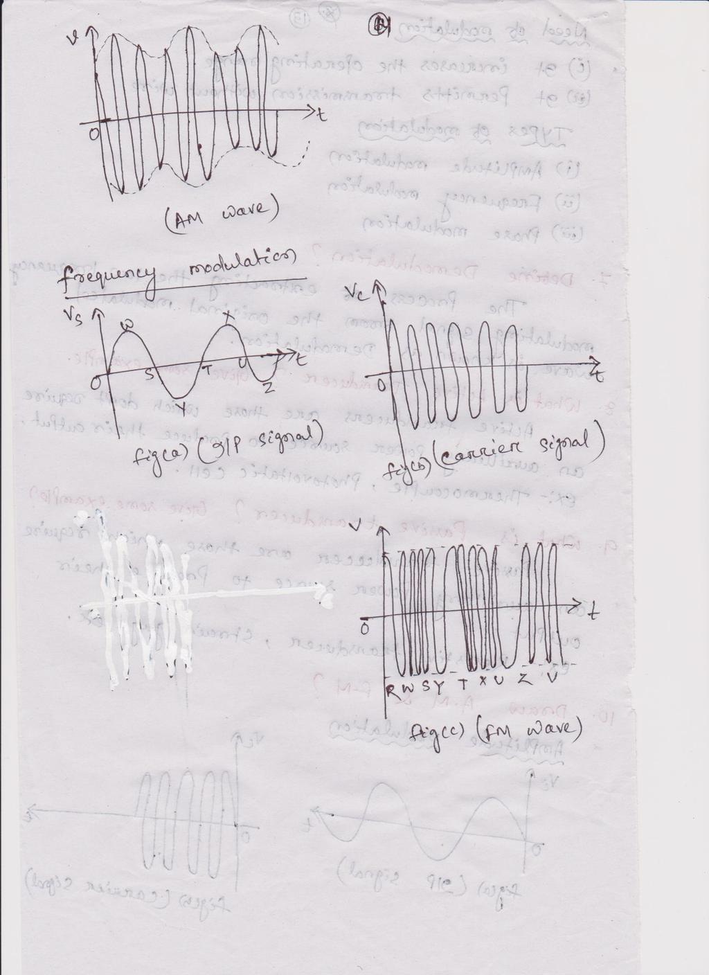
21 To synchronize horizontal deflection starts at the same point of the i/p vertical signal each time it sweeps, a synchronizing or triggering circuit is used. This ckt is link between the vertical i/p & horizontal time base. 13. Explain the operation of multimeter as voltmeter, ammeter and ohmmeter with proper diagrams. [2017w] Ans. Multimeter : It is of two types : This is the most commonly used instrument by technicians and engineers in laboratory as well as other repair works. This instrument can make many (multi) measurements with reasonable accuracy such as A.C & D. C voltages, currents & resistances. Since it is a milliam meter, voltmeter & ohmmeter combined together, so it is also called AVO meter. 1) Analog Multimeter 2) Digital Multimeter Analog Multimeter : To measure AC voltage a ractifier is connected in between input and moving system i.e galvanometer provided a series resistance when it is use to measure DC voltage. For measurement of DC current a shunt resistance is connected across the moving coil galvanometer. For measurement of AC current a rectifier is connected in between input and moving system. Digital Multimeter : For measurement of resistance a DC battery is connected in series with moving system. Digital multimeter contains typical number of moving parts. When a voltage or current passes through the meter, it converts them into a digital code (numerical code). The ckt used is called A/D converter. The code is then processed electronically to calculate the current or voltage. Digital multimeter display s the digital value of measurement automatically with decimal point. 14. Explain briefly Amplitude Modulation and Frequency Modulation. [2015W(N), 2016, 2017] Ans. Amplitude modulation: Definition: The process by which the amplitude of a carrier wave is varied in accordance with the modulating signal is called amplitude modulation. When a signal of frequency fs is modulated with carrier wave of frequency Fc, a resultant wave i.e modulated wave is produced. It retains the frequency of carrier wave i.e Fc, but it s amplitude varies in accordance with the message signal. Frequency Modulation: Definition: The process by which the frequency of a carrier wave is varied in accordance with the modulating signal is called frequency modulation. { 21 }
22 In frequency modulation the amplitude of the carrier wave (Vc) retains constant but it s frequency varies in accordance with the instantaneous magnitude of the signal. When the signal voltage is Zero the frequency of the carrier wave is not modulated & remains the same position [RSTU & V in fig.(c)] When the magnitude of signal is reaching it s +ve peak value, the frequency of the carrier wave (after modulation) also increases as represented by closely spaced cycles (Position W & X in fig (c)] Where as, during -ve peak value, the frequency of carrier decreased as represented by spaced cycles (Position Y & Z in fig (c)] { 22 }

23

24

25

26

27

28

29

30

31

32

33

34

35
36
SUMMER 13 EXAMINATION Subject Code: Model Answer Page No: / N
 Important Instructions to examiners: 1) The answers should be examined by key words and not as word-to-word as given in the model answer scheme. 2) The model answer and the answer written by candidate
Module 04.(B1) Electronic Fundamentals
 Electronic Fundamentals") 1.1a. Semiconductors - Diodes. Module 04.(B1) Electronic Fundamentals Question Number. 1. What gives the colour of an LED?. Option A. The active element. Option B. The plastic it is encased in. Option
1.1a. Semiconductors - Diodes. Module 04.(B1) Electronic Fundamentals Question Number. 1. What gives the colour of an LED?. Option A. The active element. Option B. The plastic it is encased in. Option
EXPERIMENTS USING SEMICONDUCTOR DIODES
 EXPERIMENT 9 EXPERIMENTS USING SEMICONDUCTOR DIODES Semiconductor Diodes Structure 91 Introduction Objectives 92 Basics of Semiconductors Revisited 93 A p-n Junction Operation of a p-n Junction A Forward
Downloaded from
 SOLID AND SEMICONDUCTOR DEVICES (EASY AND SCORING TOPIC) 1. Distinction of metals, semiconductor and insulator on the basis of Energy band of Solids. 2. Types of Semiconductor. 3. PN Junction formation
Sharjah Indian School, Sharjah ELECTRONIC DEVICES - Class XII (Boys Wing) Page 01
 Page 01") ELECTRONIC DEVICES - Class XII (Boys Wing) Page 01 Electronics is the fast developing branch of Physics. Before the discovery of transistors in 1948, vacuum tubes (thermionic valves) were used as the building
ELECTRONIC DEVICES - Class XII (Boys Wing) Page 01 Electronics is the fast developing branch of Physics. Before the discovery of transistors in 1948, vacuum tubes (thermionic valves) were used as the building
1) A silicon diode measures a low value of resistance with the meter leads in both positions. The trouble, if any, is
 A silicon diode measures a low value of resistance with the meter leads in both positions. The trouble, if any, is") 1) A silicon diode measures a low value of resistance with the meter leads in both positions. The trouble, if any, is A [ ]) the diode is open. B [ ]) the diode is shorted to ground. C [v]) the diode is
1) A silicon diode measures a low value of resistance with the meter leads in both positions. The trouble, if any, is A [ ]) the diode is open. B [ ]) the diode is shorted to ground. C [v]) the diode is
 Energy band diagrams Metals: 9. ELECTRONIC DEVICES GIST ρ= 10-2 to 10-8 Ω m Insulators: ρ> 10 8 Ω m Semiconductors ρ= 1 to 10 5 Ω m 109 A. Intrinsic semiconductors At T=0k it acts as insulator At room
 Electronic Devices 1. Current flowing in each of the following circuits A and respectively are: (Circuit 1) (Circuit 2) 1) 1A, 2A 2) 2A, 1A 3) 4A, 2A 4) 2A, 4A 2. Among the following one statement is not
Electronic Circuits I. Instructor: Dr. Alaa Mahmoud
 Electronic Circuits I Instructor: Dr. Alaa Mahmoud alaa_y_emam@hotmail.com Chapter 27 Diode and diode application Outline: Semiconductor Materials The P-N Junction Diode Biasing P-N Junction Volt-Ampere
BASIC ELECTRONICS ENGINEERING
 BASIC ELECTRONICS ENGINEERING Objective Questions UNIT 1: DIODES AND CIRCUITS 1 2 3 4 5 6 7 8 9 10 11 12 The process by which impurities are added to a pure semiconductor is A. Diffusing B. Drift C. Doping
MAHARASHTRA STATE BOARD OF TECHNICAL EDUCATION (Autonomous) (ISO/IEC Certified) Subject Code: Model Answer Page No: 1/
 (ISO/IEC Certified) Subject Code: Model Answer Page No: 1/") MAHARASHTRA STATE BOARD OF TECHNICAL EDUCATION (Autonomous) (ISO/IEC 27001 2005 Certified) SUMMER 13 EXAMINATION Subject Code: 12025 Model Answer Page No: 1/ Important Instructions to examiners: 1) The
MAHARASHTRA STATE BOARD OF TECHNICAL EDUCATION (Autonomous) (ISO/IEC 27001 2005 Certified) SUMMER 13 EXAMINATION Subject Code: 12025 Model Answer Page No: 1/ Important Instructions to examiners: 1) The
Chapter Semiconductor Electronics
 Chapter Semiconductor Electronics Q1. p-n junction is said to be forward biased, when [1988] (a) the positive pole of the battery is joined to the p- semiconductor and negative pole to the n- semiconductor
Section:A Very short answer question
 Section:A Very short answer question 1.What is the order of energy gap in a conductor, semi conductor, and insulator?. Conductor - no energy gap Semi Conductor - It is of the order of 1 ev. Insulator -
UNIT IX ELECTRONIC DEVICES
 UNT X ELECTRONC DECES Weightage Marks : 07 Semiconductors Semiconductors diode-- characteristics in forward and reverse bias, diode as rectifier. - characteristics of LED, Photodiodes, solarcell and Zener
MAHARASHTRA STATE BOARD OF TECHNICAL EDUCATION (Autonomous) (ISO/IEC Certified) Summer 2016 EXAMINATIONS.
 (ISO/IEC Certified) Summer 2016 EXAMINATIONS.") Summer 2016 EXAMINATIONS Subject Code: 17321 Model Answer Important Instructions to examiners: 1) The answers should be examined by key words and not as word-to-word as given in the answer scheme. 2) The
Summer 2016 EXAMINATIONS Subject Code: 17321 Model Answer Important Instructions to examiners: 1) The answers should be examined by key words and not as word-to-word as given in the answer scheme. 2) The
Shankersinh Vaghela Bapu Institute of Technology INDEX
 Shankersinh Vaghela Bapu Institute of Technology Diploma EE Semester III 3330905: ELECTRONIC COMPONENTS AND CIRCUITS INDEX Sr. No. Title Page Date Sign Grade 1 Obtain I-V characteristic of Diode. 2 To
MAHARASHTRA STATE BOARD OF TECHNICAL EDUCATION (Autonomous) (ISO/IEC Certified)
 (ISO/IEC Certified)") WINTER 16 EXAMINATION Model Answer Subject Code: 17213 Important Instructions to examiners: 1) The answers should be examined by key words and not as word-to-word as given in the model answer scheme. 2)
WINTER 16 EXAMINATION Model Answer Subject Code: 17213 Important Instructions to examiners: 1) The answers should be examined by key words and not as word-to-word as given in the model answer scheme. 2)
This tutorial will suit all beginners who want to learn the fundamental concepts of transistors and transistor amplifier circuits.
 About the Tutorial An electronic signal contains some information which cannot be utilized if doesn t have proper strength. The process of increasing the signal strength is called as Amplification. Almost
DE52/DC52 FUNDAMENTALS OF ELECTRICAL & ELECT ENGG DEC 2014
 Q.2 a. Derive an expression for the current flowing at any instant during the discharge of a capacitor C across a resistor R. b. The coil of a moving coil instrument is wound with 50 turns of wire. The
Objective Type Questions 1. Why pure semiconductors are insulators at 0 o K? 2. What is effect of temperature on barrier voltage? 3.
 Objective Type Questions 1. Why pure semiconductors are insulators at 0 o K? 2. What is effect of temperature on barrier voltage? 3. What is difference between electron and hole? 4. Why electrons have
WINTER 14 EXAMINATION. Model Answer. 1) The answers should be examined by key words and not as word-to-word as given in the
 The answers should be examined by key words and not as word-to-word as given in the") WINTER 14 EXAMINATION Subject Code: 17213 Model Answer Important Instructions to examiners: 1) The answers should be examined by key words and not as word-to-word as given in the model answer scheme. 2)
WINTER 14 EXAMINATION Subject Code: 17213 Model Answer Important Instructions to examiners: 1) The answers should be examined by key words and not as word-to-word as given in the model answer scheme. 2)
Chapter 14 Semiconductor Electronics Materials Devices And Simple Circuits
 Class XII Chapter 14 Semiconductor Electronics Materials Devices And Simple Circuits Physics Question 14.1: In an n-type silicon, which of the following statement is true: (a) Electrons are majority carriers
13. SEMICONDUCTOR DEVICES
 Synopsis: 13. SEMICONDUCTOR DEVICES 1. Solids are classified into two categories. a) Crystalline solids b) Amorphous solids 2. Crystalline solids : Crystalline solids have orderly arrangement of atoms
SRM INSTITUTE OF SCIENCE AND TECHNOLOGY (DEEMED UNIVERSITY)
") SRM INSTITUTE OF SCIENCE AND TECHNOLOGY (DEEMED UNIVERSITY) QUESTION BANK I YEAR B.Tech (II Semester) ELECTRONIC DEVICES (COMMON FOR EC102, EE104, IC108, BM106) UNIT-I PART-A 1. What are intrinsic and
SRM INSTITUTE OF SCIENCE AND TECHNOLOGY (DEEMED UNIVERSITY) QUESTION BANK I YEAR B.Tech (II Semester) ELECTRONIC DEVICES (COMMON FOR EC102, EE104, IC108, BM106) UNIT-I PART-A 1. What are intrinsic and
MAHARASHTRA STATE BOARD OF TECHNICAL EDUCATION (Autonomous) (ISO/IEC Certified) MODEL ANSWER
 (ISO/IEC Certified) MODEL ANSWER") Important Instructions to examiners: 1) The answers should be examined by key words and not as word-to-word as given in the model answer scheme. 2) The model answer and the answer written by candidate
Important Instructions to examiners: 1) The answers should be examined by key words and not as word-to-word as given in the model answer scheme. 2) The model answer and the answer written by candidate
Summer 2015 Examination. 1) The answers should be examined by key words and not as word-to-word as given in the model answer scheme.
 The answers should be examined by key words and not as word-to-word as given in the model answer scheme.") Summer 2015 Examination Subject Code: 17213 Model Answer Important Instructions to examiners: 1) The answers should be examined by key words and not as word-to-word as given in the model answer scheme.
Summer 2015 Examination Subject Code: 17213 Model Answer Important Instructions to examiners: 1) The answers should be examined by key words and not as word-to-word as given in the model answer scheme.
 SEMICONDUCTOR EECTRONICS MATERIAS, DEVICES AND SIMPE CIRCUITS Important Points: 1. In semiconductors Valence band is almost filled and the conduction band is almost empty. The energy gap is very small
UNIT-I SEMICONDUCTOR DEVICES
 SEMICONDUCTOR MATERIALS: UNIT-I SEMICONDUCTOR DEVICES INSULATOR: An insulator is a material that offers a very low level of conductivity under Pressure from an applied voltage source. In this material
ELECTRONIC DEVICES MARKS WEIGHTAGE 7 marks
 ELECTRONIC DEVICES MARKS WEIGHTAGE 7 marks QUICK REVISION (Important Concepts & Formulas) Electronics It is the branch of science, which deals with the study of flow and control of electrons through a
PHYS 3050 Electronics I
 PHYS 3050 Electronics I Chapter 4. Semiconductor Diodes and Transistors Earth, Moon, Mars, and Beyond Dr. Jinjun Shan, Associate Professor of Space Engineering Department of Earth and Space Science and
Lesson Plan. Week Theory Practical Lecture Day. Topic (including assignment / test) Day. Thevenin s theorem, Norton s theorem
 Day. Thevenin s theorem, Norton s theorem") Name of the faculty: GYANENDRA KUMAR YADAV Discipline: APPLIED SCIENCE(C.S.E,E.E.ECE) Year : 1st Subject: FEEE Lesson Plan Lesson Plan Duration: 31 weeks (from July, 2018 to April, 2019) Week Theory Practical
Name of the faculty: GYANENDRA KUMAR YADAV Discipline: APPLIED SCIENCE(C.S.E,E.E.ECE) Year : 1st Subject: FEEE Lesson Plan Lesson Plan Duration: 31 weeks (from July, 2018 to April, 2019) Week Theory Practical
EDC Lecture Notes UNIT-1
 P-N Junction Diode EDC Lecture Notes Diode: A pure silicon crystal or germanium crystal is known as an intrinsic semiconductor. There are not enough free electrons and holes in an intrinsic semi-conductor
ELECTRONIC DEVICES AND CIRCUITS
 ELECTRONIC DEVICES AND CIRCUITS 1. At room temperature the current in an intrinsic semiconductor is due to A. holes B. electrons C. ions D. holes and electrons 2. Work function is the maximum energy required
Table of Contents. iii
 Table of Contents Subject Page Experiment 1: Diode Characteristics... 1 Experiment 2: Rectifier Circuits... 7 Experiment 3: Clipping and Clamping Circuits 17 Experiment 4: The Zener Diode 25 Experiment
SETH JAI PARKASH POLYTECHNIC, DAMLA
 SETH JAI PARKASH POLYTECHNIC, DAMLA NAME OF FACULTY----------SANDEEP SHARMA DISCIPLINE---------------------- E.C.E (S.F) SEMESTER-------------------------2 ND SUBJECT----------------------------BASIC ELECTRONICS
Subject Code: Model Answer Page No: / N
 Important Instructions to examiners: 1) The answers should be examined by key words and not as word-to-word as given in the model answer scheme. 2) The model answer and the answer written by candidate
FINALTERM EXAMINATION. Spring PHY301- Circuit Theory
 Date 14/2/2013 Eini FINALTERM EXAMINATION Spring 2010 PHY301- Circuit Theory Time: 90 min Marks: 60 Question No: 1 If we connect 3 capacitors in parallel, the combined effect of all these capacitors will
CHAPTER 9: ELECTRONICS
 CHAPTER 9: ELECTRONICS 9.1 Cathode Rays 9.1.1 Thermionic Emission Thermionic emission is the emission of electrons from a heated metal surface. Factors that influence the rate of thermionic emission: Temperature
Discuss the basic structure of atoms Discuss properties of insulators, conductors, and semiconductors
 Discuss the basic structure of atoms Discuss properties of insulators, conductors, and semiconductors Discuss covalent bonding Describe the properties of both p and n type materials Discuss both forward
Intrinsic Semiconductor
 Semiconductors Crystalline solid materials whose resistivities are values between those of conductors and insulators. Good electrical characteristics and feasible fabrication technology are some reasons
Basic Electronics SYLLABUS BASIC ELECTRONICS. Subject Code : 15ELN15/25 IA Marks : 20. Hrs/Week : 04 Exam Hrs. : 03. Total Hrs. : 50 Exam Marks : 80
 SYLLABUS BASIC ELECTRONICS Subject Code : /25 IA Marks : 20 Hrs/Week : 04 Exam Hrs. : 03 Total Hrs. : 50 Exam Marks : 80 Course objectives: The course objective is to make students of all the branches
Lesson 08. Name and affiliation of the author: Professor L B D R P Wijesundera Department of Physics, University of Kelaniya.
 Lesson 08 Title of the Experiment: Identification of active components in electronic circuits and characteristics of a Diode, Zener diode and LED (Activity number of the GCE Advanced Level practical Guide
Basic Electronics: Diodes and Transistors. October 14, 2005 ME 435
 Basic Electronics: Diodes and Transistors Eşref Eşkinat E October 14, 2005 ME 435 Electric lectricity ity to Electronic lectronics Electric circuits are connections of conductive wires and other devices
CHAPTER FORMULAS & NOTES
 Formulae For u SEMICONDUCTORS By Mir Mohammed Abbas II PCMB 'A' 1 Important Terms, Definitions & Formulae CHAPTER FORMULAS & NOTES 1 Intrinsic Semiconductor: The pure semiconductors in which the electrical
15 - SEMICONDUCTOR ELECTRONICS: MATERIALS, DEVICES AND SIMPLE CIRCUITS Page 1
 15.1 Introduction MATERIALS, DEVICES AND SIMPLE CIRCUITS Page 1 The word electronics is coined from the words electron mechanics. The subject of electronics deals with the study of devices in which specific
State the application of negative feedback and positive feedback (one in each case)
") (ISO/IEC - 700-005 Certified) Subject Code: 073 Model wer Page No: / N Important Instructions to examiners: ) The answers should be examined by key words and not as word-to-word as given in the model answer
(ISO/IEC - 700-005 Certified) Subject Code: 073 Model wer Page No: / N Important Instructions to examiners: ) The answers should be examined by key words and not as word-to-word as given in the model answer
UNIT 3 Transistors JFET
 UNIT 3 Transistors JFET Mosfet Definition of BJT A bipolar junction transistor is a three terminal semiconductor device consisting of two p-n junctions which is able to amplify or magnify a signal. It
 Code No: Y0221/R07 Set No. 1 I B.Tech Supplementary Examinations, Apr/May 2013 BASIC ELECTRONIC DEVICES AND CIRCUITS (Electrical & Electronics Engineering) Time: 3 hours Max Marks: 80 Answer any FIVE Questions
Diode Limiters or Clipper Circuits
 Diode Limiters or Clipper Circuits Circuits which are used to clip off portions of signal voltages above or below certain levels are called limiters or clippers. Types of Clippers Positive Clipper Negative
Summer 2015 Examination. 1) The answers should be examined by key words and not as word-to-word as given in the model answer scheme.
 The answers should be examined by key words and not as word-to-word as given in the model answer scheme.") Summer 2015 Examination Subject Code: 17215 Model Answer Important Instructions to examiners: 1) The answers should be examined by key words and not as word-to-word as given in the model answer scheme.
Summer 2015 Examination Subject Code: 17215 Model Answer Important Instructions to examiners: 1) The answers should be examined by key words and not as word-to-word as given in the model answer scheme.
Diode conducts when V anode > V cathode. Positive current flow. Diodes (and transistors) are non-linear device: V IR!
 are non-linear device: V IR!") Diodes: What do we use diodes for? Lecture 5: Diodes and Transistors protect circuits by limiting the voltage (clipping and clamping) turn AC into DC (voltage rectifier) voltage multipliers (e.g. double
Diodes: What do we use diodes for? Lecture 5: Diodes and Transistors protect circuits by limiting the voltage (clipping and clamping) turn AC into DC (voltage rectifier) voltage multipliers (e.g. double
Downloaded from Downloaded from
 IV SEMESTER FINAL EXAMINATION-2002 The figure in the margin indicates full marks. [i] (110111) 2 = (?) 16 [ii] (788) 10 = (?) 8 Q. [1] [a] Explain the types of extrinsic semiconductors with the help of
Lecture -1: p-n Junction Diode
 Lecture -1: p-n Junction Diode Diode: A pure silicon crystal or germanium crystal is known as an intrinsic semiconductor. There are not enough free electrons and holes in an intrinsic semi-conductor to
TEACHING & EXAMINATION SCHEME For the Examination 2015 ELECTRONICS. B.Sc. Part - I
 TEACHING & EXAMINATION SCHEME For the Examination 2015 ELECTRONICS THEORY B.Sc. Part - I Elec. 101 Paper I Circuit Elements and Networks Pd/W Exam. Max. (45mts.) Hours Marks 150 2 3 50 Elec. 102 Paper
Università degli Studi di Roma Tor Vergata Dipartimento di Ingegneria Elettronica. Analogue Electronics. Paolo Colantonio A.A.
 Università degli Studi di Roma Tor Vergata Dipartimento di Ingegneria Elettronica Analogue Electronics Paolo Colantonio A.A. 2015-16 Introduction: materials Conductors e.g. copper or aluminum have a cloud
Unit - 19 Semiconductor Electronics
 Unit - 19 Semiconductor Electronics 321 Conductor :- Presence of free electrons Electrical resistivity is quite less Insulator :- No free electrons Very large electrical resistivity Semi-conductor :- Hole
Scheme Q.1 Attempt any SIX of following 12-Total Marks 1 A) Draw symbol of P-N diode, Zener diode. 2 M Ans: P-N diode
 Draw symbol of P-N diode, Zener diode. 2 M Ans: P-N diode") Q. No. WINTER 16 EXAMINATION (Subject Code: 17321) Model Answer Important Instructions to examiners: 1) The answers should be examined by key words and not as word-to-word as given in themodel answer scheme.
Q. No. WINTER 16 EXAMINATION (Subject Code: 17321) Model Answer Important Instructions to examiners: 1) The answers should be examined by key words and not as word-to-word as given in themodel answer scheme.
EC6202- ELECTRONIC DEVICES AND CIRCUITS UNIT TEST-1 EXPECTED QUESTIONS
 EC6202- ELECTRONIC DEVICES AND CIRCUITS UNIT TEST-1 EXPECTED QUESTIONS 1. List the PN diode parameters. 1. Bulk Resistance. 2. Static Resistance/Junction Resistance (or) DC Forward Resistance 3. Dynamic
MODEL ANSWER SUMMER 17 EXAMINATION 17213
 MODEL ANSWER SUMMER 17 EXAMINATION 17213 Subject Title: Basic Electronics Subject Code: Important Instructions to examiners: 1) The answers should be examined by key words and not as word-to-word as given
Diode Bridges. Book page
 Diode Bridges Book page 450-454 Rectification The process of converting an ac supply into dc is called rectification The device that carries this out is called a rectifier Half wave rectifier only half
Analog Electronic Circuits
 Analog Electronic Circuits Chapter 1: Semiconductor Diodes Objectives: To become familiar with the working principles of semiconductor diode To become familiar with the design and analysis of diode circuits
WINTER 17 EXAMINATION Subject Name: Basic Electronics Model Answer Sub Code:
 Important Instructions to examiners: 1) The answers should be examined by key words and not as word-to-word as given in the model answer scheme. 2) The model answer and the answer written by candidate
NEW HORIZON PRE UNIVERSITY COLLEGE LESSON PLAN FOR THE ACADEMIC YEAR Department of ELECTRONICS
 NEW HORIZON PRE UNIVERSITY COLLEGE LESSON PLAN FOR THE ACADEMIC YEAR 2017 2018 Department of ELECTRONICS I PUC Month: JUNE I 1. INTRODUCTION TO ELECTRONICS Electronics and its scope: Development of vacuum
SEMICONDUCTOR ELECTRONICS: MATERIALS, DEVICES AND SIMPLE CIRCUITS. Class XII : PHYSICS WORKSHEET
 SEMICONDUCT ELECTRONICS: MATERIALS, DEVICES AND SIMPLE CIRCUITS Class XII : PHYSICS WKSHEET 1. How is a n-p-n transistor represented symbolically? (1) 2. How does conductivity of a semiconductor change
Electronic devices-i. Difference between conductors, insulators and semiconductors
 Electronic devices-i Semiconductor Devices is one of the important and easy units in class XII CBSE Physics syllabus. It is easy to understand and learn. Generally the questions asked are simple. The unit
Scheme Q.1 Attempt any SIX of following: 12-Total Marks a) Draw symbol NPN and PNP transistor. 2 M Ans: Symbol Of NPN and PNP BJT (1M each)
 Draw symbol NPN and PNP transistor. 2 M Ans: Symbol Of NPN and PNP BJT (1M each)") Q. No. WINTER 16 EXAMINATION (Subject Code: 17319) Model Answer Important Instructions to examiners: 1) The answers should be examined by key words and not as word-to-word as given in the model answer
Q. No. WINTER 16 EXAMINATION (Subject Code: 17319) Model Answer Important Instructions to examiners: 1) The answers should be examined by key words and not as word-to-word as given in the model answer
Code No: R Set No. 1
 Code No: R05010204 Set No. 1 I B.Tech Supplimentary Examinations, Aug/Sep 2007 ELECTRONIC DEVICES AND CIRCUITS ( Common to Electrical & Electronic Engineering, Electronics & Communication Engineering,
Examples to Power Supply
 Examples to Power Supply Example-1: A center-tapped full-wave rectifier connected to a transformer whose each secondary coil has a r.m.s. voltage of 1 V. Assume the internal resistances of the diode and
Shankersinh Vaghela Bapu Institute of Technology
 Shankersinh Vaghela Bapu Institute of Technology B.E. Semester III (EC) 131101: Basic Electronics INDEX Sr. No. Title Page Date Sign Grade 1 [A] To Study the V-I characteristic of PN junction diode. [B]
F.Y. Diploma : Sem. II [CO/CD/CM/CW/IF] Basic Electronics
![F.Y. Diploma : Sem. II [CO/CD/CM/CW/IF] Basic Electronics](/thumbs/78/77332946.jpg "F.Y. Diploma : Sem. II [CO/CD/CM/CW/IF] Basic Electronics") F.Y. Diploma : Sem. II [CO/CD/CM/CW/IF] Basic Electronics Time : 3 Hrs.] Prelim Question Paper Solutions [Marks : 100 Q.1 Attempt any TEN of the following : [20] Q.1(a) Give the classification of capacitor.
F.Y. Diploma : Sem. II [CO/CD/CM/CW/IF] Basic Electronics Time : 3 Hrs.] Prelim Question Paper Solutions [Marks : 100 Q.1 Attempt any TEN of the following : [20] Q.1(a) Give the classification of capacitor.
MAHARASHTRA STATE BOARD OF TECHNICAL EDUCATION (Autonomous) (ISO/IEC Certified)
 (ISO/IEC Certified)") WINTER 18 EXAMINATION Subject Name: Basic Electronics Model Answer Subject Code: 17321 I m p o r t a n t I n s t r u c t i o n s t o e x a m i n e r s : 1) The answers should be examined by key words and
WINTER 18 EXAMINATION Subject Name: Basic Electronics Model Answer Subject Code: 17321 I m p o r t a n t I n s t r u c t i o n s t o e x a m i n e r s : 1) The answers should be examined by key words and
Lesson 5. Electronics: Semiconductors Doping p-n Junction Diode Half Wave and Full Wave Rectification Introduction to Transistors-
 Lesson 5 Electronics: Semiconductors Doping p-n Junction Diode Half Wave and Full Wave Rectification Introduction to Transistors- Types and Connections Semiconductors Semiconductors If there are many free
SYED AMMAL ENGINEERING COLLEGE
 SYED AMMAL ENGINEERING COLLEGE (Approved by the AICTE, New Delhi, Govt. of Tamilnadu and Affiliated to Anna University, Chennai) Established in 1998 - An ISO 9001:2008 Certified Institution Dr. E.M.Abdullah
Student Lecture by: Giangiacomo Groppi Joel Cassell Pierre Berthelot September 28 th 2004
 Student Lecture by: Giangiacomo Groppi Joel Cassell Pierre Berthelot September 28 th 2004 Lecture outline Historical introduction Semiconductor devices overview Bipolar Junction Transistor (BJT) Field
Class XII - Physics Semiconductor Electronics. Chapter-wise Problems
 lass X - Physics Semiconductor Electronics Materials, Device and Simple ircuit hapter-wise Problems Multiple hoice Question :- 14.1 The conductivity of a semiconductor increases with increase in temperature
INSTITUTE OF AERONAUTICAL ENGINEERING Dundigal, Hyderabad
 Course Name Course Code Class Branch INSTITUTE OF AERONAUTICAL ENGINEERING Dundigal, Hyderabad -500 043 AERONAUTICAL ENGINEERING TUTORIAL QUESTION BANK : ELECTRICAL AND ELECTRONICS ENGINEERING : A40203
ELECTRONICS ENGINEERING
 ELECTRONICS ENGINEERING 1. Just as a voltage amplifier signal voltage a power amplifier. 1.amplifier power 2.amplifier signal 3.converts the signal ac power into DC power 4.converts a dc power into useful
Experiments in Analog Electronics
 Ministry of Higher Education and Scientific Research University of Technology Department of Electrical Engineering Analog Electronics Laboratory Experiments in Analog Electronics By Firas Mohammed Ali
Pre-certification Electronics Questions. Answer the following with the MOST CORRECT answer.
 Electronics Questions Answer the following with the MOST CORRECT answer. 1. The cathode end terminal of a semiconductor diode can be identified by: a. the negative sign marked on the case b. a circular
070 ELECTRONICS WORKS EXAMINATION STRUCTURE
 070 ELECTRONICS WORKS EXAMINATION STRUCTURE The trade will be examined under the following components or subject grouping: Electronic Devices and Circuit, Radio Communication and Television. EXAMINATION
CHAPTER 1 DIODE CIRCUITS. Semiconductor act differently to DC and AC currents
 CHAPTER 1 DIODE CIRCUITS Resistance levels Semiconductor act differently to DC and AC currents There are three types of resistances 1. DC or static resistance The application of DC voltage to a circuit
ELECTRICITY AND ELECTRONICS
 ELECTRICITY AND ELECTRONICS (Maximum Marks: 100) (Time allowed: Three hours) (Candidates are allowed additional 15 minutes for only reading the paper. They must NOT start writing during this time.) Answer
Basic Electronics Prof. T.S. Natarajan Department of Physics Indian Institute of Technology, Madras
 Basic Electronics Prof. T.S. Natarajan Department of Physics Indian Institute of Technology, Madras Lecture 39 Silicon Controlled Rectifier (SCR) (Construction, characteristics (Dc & Ac), Applications,
CENTURION UNIVERSITY OF TECHNOLOGY AND MANAGEMENT SCHOOL OF ENGINEERING & TECHNOLOGYDEPARTMENT OF ELECTRONICS & COMMUNICATION ENGINEERING
 CENTURION UNIVERSITY OF TECHNOLOGY AND MANAGEMENT SCHOOL OF ENGINEERING & TECHNOLOGYDEPARTMENT OF ELECTRONICS & COMMUNICATION ENGINEERING ELECTRONIC DEVICES Section: ECE SEM: II PART-A 1. a) In a N-type
Practical Manual. Deptt.of Electronics &Communication Engg. (ECE)
") Practical Manual LAB: BASICS OF ELECTRONICS 1 ST SEM.(CSE/CV) Deptt.of Electronics &Communication Engg. (ECE) RAO PAHALD SINGH GROUP OF INSTITUTIONS BALANA(MOHINDER GARH)12302 Prepared By. Mr.SANDEEP KUMAR
Practical Manual LAB: BASICS OF ELECTRONICS 1 ST SEM.(CSE/CV) Deptt.of Electronics &Communication Engg. (ECE) RAO PAHALD SINGH GROUP OF INSTITUTIONS BALANA(MOHINDER GARH)12302 Prepared By. Mr.SANDEEP KUMAR
PAST EXAM PAPER & MEMO N3 ABOUT THE QUESTION PAPERS:
 EKURHULENI TECH COLLEGE. No. 3 Mogale Square, Krugersdorp. Website: www. ekurhulenitech.co.za Email: info@ekurhulenitech.co.za TEL: 011 040 7343 CELL: 073 770 3028/060 715 4529 PAST EXAM PAPER & MEMO N3
UNIT 3: FIELD EFFECT TRANSISTORS
 FIELD EFFECT TRANSISTOR: UNIT 3: FIELD EFFECT TRANSISTORS The field effect transistor is a semiconductor device, which depends for its operation on the control of current by an electric field. There are
Basic Electronics Learning by doing Prof. T.S. Natarajan Department of Physics Indian Institute of Technology, Madras
 Basic Electronics Learning by doing Prof. T.S. Natarajan Department of Physics Indian Institute of Technology, Madras Lecture 38 Unit junction Transistor (UJT) (Characteristics, UJT Relaxation oscillator,
QUESTION BANK EC6201 ELECTRONIC DEVICES UNIT I SEMICONDUCTOR DIODE PART A. It has two types. 1. Intrinsic semiconductor 2. Extrinsic semiconductor.
 FATIMA MICHAEL COLLEGE OF ENGINEERING & TECHNOLOGY Senkottai Village, Madurai Sivagangai Main Road, Madurai - 625 020. [An ISO 9001:2008 Certified Institution] QUESTION BANK EC6201 ELECTRONIC DEVICES SEMESTER:
Vidyalankar F.Y. Diploma : Sem. II [CO/CD/CM/CW/IF] Basic Electronics V F V K. V K = 0.7 for Si = 0.3 for Ge
![Vidyalankar F.Y. Diploma : Sem. II [CO/CD/CM/CW/IF] Basic Electronics V F V K. V K = 0.7 for Si = 0.3 for Ge](/thumbs/94/121292009.jpg "Vidyalankar F.Y. Diploma : Sem. II [CO/CD/CM/CW/IF] Basic Electronics V F V K. V K = 0.7 for Si = 0.3 for Ge") F.Y. Diploma : Sem. II [CO/CD/CM/CW/IF] Basic Electronics Time : 3 Hrs. Prelim Question Paper Solution Marks : 100 Q.1 Attempt any TEN of the following: [20] Q.1(a) Draw characteristics of PN junction
F.Y. Diploma : Sem. II [CO/CD/CM/CW/IF] Basic Electronics Time : 3 Hrs. Prelim Question Paper Solution Marks : 100 Q.1 Attempt any TEN of the following: [20] Q.1(a) Draw characteristics of PN junction
Emitter base bias. Collector base bias Active Forward Reverse Saturation forward Forward Cut off Reverse Reverse Inverse Reverse Forward
 SEMICONDUCTOR PHYSICS-2 [Transistor, constructional characteristics, biasing of transistors, transistor configuration, transistor as an amplifier, transistor as a switch, transistor as an oscillator] Transistor
MAHARASHTRA STATE BOARD OF TECHNICAL EDUCATION (Autonomous) (ISO/IEC Certified) Summer 2016 EXAMINATIONS
 (ISO/IEC Certified) Summer 2016 EXAMINATIONS") Summer 2016 EXAMINATIONS Subject Code: 17213 Model Answer Important Instructions to examiners: 1) The answers should be examined by key words and not as word-to-word as given in the answer scheme. 2) The
Summer 2016 EXAMINATIONS Subject Code: 17213 Model Answer Important Instructions to examiners: 1) The answers should be examined by key words and not as word-to-word as given in the answer scheme. 2) The
Semiconductor Devices
 About the Tutorial The electronic components exploiting the electronic properties of semiconductor materials, are termed as semiconductor devices. This tutorial discusses the functional operation of semiconductor
Maltase cross tube. D. Senthilkumar P a g e 1
 Thermionic Emission Maltase cross tube Definition: The emission of electrons when a metal is heated to a high temperature Explanation: In metals, there exist free electrons which are able to move around
Downloaded from
 Question 14.1: In an n-type silicon, which of the following statement is true: (a) Electrons are majority carriers and trivalent atoms are the dopants. (b) Electrons are minority carriers and pentavalent
THERMIONIC AND GASEOUS STATE DIODES
 THERMIONIC AND GASEOUS STATE DIODES Thermionic and gaseous state (vacuum tube) diodes Thermionic diodes are thermionic-valve devices (also known as vacuum tubes, tubes, or valves), which are arrangements
EE70 - Intro. Electronics
 EE70 - Intro. Electronics Course website: ~/classes/ee70/fall05 Today s class agenda (November 28, 2005) review Serial/parallel resonant circuits Diode Field Effect Transistor (FET) f 0 = Qs = Qs = 1 2π
UNIT I PN JUNCTION DEVICES
 UNIT I PN JUNCTION DEVICES 1. Define Semiconductor. 2. Classify Semiconductors. 3. Define Hole Current. 4. Define Knee voltage of a Diode. 5. What is Peak Inverse Voltage? 6. Define Depletion Region in
Diodes. Analog Electronics Lesson 4. Objectives and Overview:
 Analog Electronics Lesson 4 Diodes Objectives and Overview: This lesson will introduce p- and n-type material, how they form a junction that rectifies current, and familiarize you with basic p-n junction
Q1 A) Attempt any six: i) Draw the neat symbol of N-channel and P-channel FET
 Attempt any six: i) Draw the neat symbol of N-channel and P-channel FET") Subject Code:17319 Model Answer Page1 of 27 Important Instructions to examiners: 1) The answers should be examined by key words and not as word-to-word as given in the model answer scheme. 2) The model
Subject Code:17319 Model Answer Page1 of 27 Important Instructions to examiners: 1) The answers should be examined by key words and not as word-to-word as given in the model answer scheme. 2) The model