Virtual Access Technique Augments Test Coverage on Limited Access PCB Assemblies
|
|
|
- Austen Goodwin
- 5 years ago
- Views:
Transcription
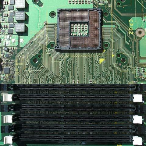
1 Virtual Access Technique Augments Test Coverage on Limited Access PCB Assemblies Anthony J. Suto Teradyne Inc. North Reading, Massachusetts Abstract Increased pressures to reduce time to market and time to volume have forced many manufacturers of populated printed circuit boards to rely on capacitively coupled, un-powered, vectorless in-circuit test techniques to identify open pins on ICs and connectors. Unfortunately, faster signals and higher-density printed circuit boards (PCBs) have placed pressures on designers to reduce the number of test pads that provide electrical access for vectorless test techniques. A powered-up test solution using boundary scan as the stimulus generator and a capacitive sensor plate for detection can address this loss of access. This virtual access method can quickly and effectively identify connectivity defects between boundary scan based ICs and other devices, including non-boundary scan devices, connectors, and sockets that lack physical test access. This test approach employs a novel set of time domain auto-correlation and cross-correlation algorithms that eliminate many of the restrictions associated with existing frequency domain alternatives. More specifically, this test method does not restrict the operating frequency of the boundary scan s clock signal (TCK) or the number of scan cells in the boundary scan chain. Analyzing the temporal response of a single event pulse in the time domain by use of matched filtering eliminates the need to generate the narrow range of stimulus frequencies that traditional capacitive sensor plate methods require. This virtual test method works with any boundary scan device that complies with the IEEE , or standards. A discussion of this test method as well as recent field data, lessons learned and obstacles overcome while implementing this technique on a high-end computer server product at a high volume production facility are disclosed. Introduction Detecting open solder connections on printed circuit board (PCB) assemblies continues to be a major challenge on today s manufacturing floor. Capacitive based vectorless techniques such as FrameScan FX TM have met the demand of finding such manufacturing defects on the majority of a PCB s solder connections. Vectorless test is a capacitive based sensing technology whereby a node on the board is excited by a low level sinusoidal signal and a capacitive sensor plate is placed proximate to the IC, socket or connector that is being interrogated for connectivity defects. This technique compares the capacitively coupled resultant signal amplitude against pre-determined test limits to determine whether there is an electrical connection to the device. This vectorless technology has become very popular in the in-circuit test industry due to the simplicity of program development and good coverage results. However, for this technique to be a viable test option, the incircuit test platform requires electrical access to the component that is being interrogated. Electrical access has been slowly deteriorating on printed circuit boards in certain market segments for some time now [1]. The affected markets include computing, networking/communications and RF. There are several factors behind this erosion of electrical access on these products. The first issue involves the increase in the PCB component I/O and wiring density and the subsequent move to employ high density interconnect (HDI) technologies on the PCB assembly in order to retain circuit connectivity. HDI boards generally exhibit line widths and spacing that are less than 4 mils with via geometries less than 6 mils and with connection densities greater than 130 pads/in 2. In addition, HDI assemblies can have small blind and buried vias and via-in-pad that allow area array packages to be connected on inner layers without exterior PCB layer access, thereby eliminating the possibility of a test pad. With such high board densities, it is simply impractical to place hundreds to thousands of conventional test pads that are 18 mils to 35 mils in diameter on the board for in-circuit test access. The second driving force that is eroding electrical access is related to the increase in signaling speed on printed circuit board traces. Many signal integrity (SI) engineers are reluctant to place test pads on high speed nets for fear of signal integrity degradation. Placing a test pad on a high speed signal creates an impedance discontinuity on the transmission line that can cause reflections and other signal degradation when the board is operating in mission mode. Test pads, when placed directly on top of the signal etch, can be compensated by placing anti-pads in the reference plane to raise the characteristic impedance at the pad to better match the line impedance, but few, if any SI engineers are willing to undergo the added simulation time and increased board complexity to implement such a compensation scheme.

2 Figure 1. Block diagram of powered opens technique With the increased loss of electrical access on certain PCB assemblies, alternative test methods can be implemented in order to retain test coverage on the assembly. Traditional IEEE boundary scan is one possible solution to the problem. Boundary scan compliant integrated circuit (IC) devices utilize built-in testability structures on the input and output device pins for the purpose of identifying typical process defects including open and shorted connections. Shorts between nets can typically be identified using boundary scan, provided that the pins of the device have self monitoring capability. Boundary scan devices that are interconnected to other scan devices can readily be tested for connectivity defects, but often times a boundary scan part connects to a socket or a connector that is vacant during the time that the assembly is being tested. These board interconnect scenarios require a different test method to regain fault coverage and pin level diagnostics. Virtual Access Test Method Powered Opens is a test technique developed several years ago that combines boundary scan and capacitive based opens technologies to create virtual access to PCB signal nets that may not have conventional test point access [2]. With this technique, a boundary scan device acts as an on-board stimulus generator while a capacitive sensor plate provides a means of detecting the resultant test signal. A high level block diagram of this combined test method is illustrated above in Figure 1. In this illustration, the test platform s digital resources are connected to the test access port, or TAP of the boundary scan device. The test system uses the TAP to initialize the device and to generate the required set of test vectors. The output stimulus consists of a single digital pulse per pin that is being tested. Whenever possible, all other pins on the device under test are held at a static logic level in order to isolate the sensor plate from any other on-board signal activity. Each pin that is tested has a unique time slot that is non-overlapping with any other pin activity to eliminate diagnostic ambiguity. The digital pulse from the boundary scan output pin is capacitively coupled to the sensor plate and is amplified by a local transimpedance amplifier that resides on top of the sensor plate. This signal is then processed through continuous time analog filters, is then digitized and then analyzed in the time domain to determine potential connectivity issues. There are two basic processes involved in identifying these connectivity defects. The first is called the learn phase, whereby a known good PCB assembly is tested to acquire the characteristic pin amplitude readings of the assembly during test program development. Typically several known good PCB assemblies are learned and an average profile is used as a reference for each connection. The second phase is the actual production test phase whereby boards of unknown quality are tested for open and short defect conditions using pass/fail thresholds that have been calculated from the learn phase.

3 Domains of Testing The boundary scan device that is used as an on-board stimulus generator can supply a repetitive signal such as a square wave, or a non-repetitive signal that can be a rising edge, a falling edge, or a pulse that combines the two edges. The signal analysis of the resultant signal can be performed in the time domain, or in the frequency domain. As a result, there are four possibilities in terms of signal generation and signal processing. The method described in this paper uses a non-repetitive pulse that is analyzed in the time domain because this combination offers a number of benefits over the other combinations as detailed below. Most vectorless capacitive opens test methods use a repetitive sinusoidal signal that is then processed in the frequency domain. The test frequency that is applied to the device under test is in the narrow range of approximately 8KHz to10khz. Applying a lower test frequency results in lower resultant signal amplitude that will ultimately decrease fault coverage. Signal frequencies above 10KHz will yield a larger signal, but can cause signal coupling between the printed circuit board and the sensor plate. The result is an increase in the quantity of false pass opportunities because the sensor plate is receiving signal strength from the board as well as from the tested component on the PCB. Frequency based testing, when applied to powered opens has a fundamental limitation in being able to successfully synthesize the minimum desired pin toggle frequencies under all board conditions. The reason for this is that the maximum boundary scan output pin toggle frequency is approximately equal to the boundary scan clock (TCK), divided by two and also divided by the number of scan cells that are active in the boundary scan chain (see Equation 1 below). Equation 1. Boundary scan output pin toggle frequency If, for example the boundary scan clock is operating at 2MHz, then a boundary scan chain with more than 125 scan cells will lower the pin toggle frequency below the desired 8KHz envelope. Increasing the frequency of the boundary scan clock is one possible solution, but specialized fixture electronics may be needed to deliver a clean clock signal to the board under test. In addition, today s devices that contain boundary scan can contain many hundreds of scan cells and the I/O count is predicted to increase in the future [3]. Utilizing a single event pulse to excite the device under test mitigates the dependency between the number of scan cells in the chain and the pin toggle frequency because the test is not constantly re-loading the scan chain to drive alternating one and zero patterns to an output pin to generate many cycles of a square wave test signal. A second advantage of using a single pulse rather than a periodic signal is that the throughput is improved. Figure 2 shows families of throughput curves as a function of the number of scan cells in the chain and the percentage of scan cells that are Figure 2. Powered opens throughput in pins tested per second

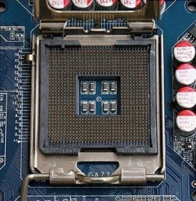
4 actually being tested using a 2MHz TCK signal. In many instances, the number of pins per second that can be tested is much greater than the traditional un-powered analog opens techniques which can typically test 500 pins per second. Signal Analysis A method of matched filtering correlates a known signal or template with the measured signal that is in question. Matched filters offer the maximum achievable signal to noise ratio (SNR) in the presence of white noise and are commonly implemented by cross correlation methods (Equation 2, second term) [4]. This signal processing technique can be found in radar signal processing and is used in this pulsed version of powered opens signal processing as well. Equation 2 details the auto correlation and cross-correlation functions where X(i) and Y(i) are the respective learned and production data vectors, Mx and My represent the mean values of these digitized data vectors and R(d) is the correlation coefficient that denotes the likelihood that the measured pin signal matches the learned reference signal in both temporal response and in magnitude. As part of the learn process during program development, multiple de-normalized auto-correlation values are calculated from the digitized data vectors for a pin and are averaged to create a reference autocorrelation coefficient and a reference data vector for the production floor cross correlation operation. The auto correlation section of the analysis also allows one to calculate the mean and standard deviation of a number of auto-correlation values to ensure that there is not excessive variation due to noise. Should there be excessive variation as indicated by a standard deviation value that is large, as compared to the mean value, the pin will be discounted from the test because the pin thresholds cannot reliably be set. The digitized data for a pin is sorted out from the digitizer s memory and reconstructed into a single long data vector (X(n)). This vector is created by simply placing the negative edge data samples directly after the last data point of the positive edge data samples. Equation 2. Denormalized autocorrelation and cross correlation, respectively During production testing, if the de-normalized cross-correlation value (Rd) is either less than or greater than the learned denormalized auto-correlation value by a certain percentage, then the pin is then deemed to be defective, otherwise the connection is considered a good one. The correlation technique that is described is very resistant to random noise in the signal which dramatically helps to reduce false calls on the manufacturer s production floor. Lessons Learned in Production As the name implies, powered opens is a test technique where at least a part of the board is powered up to allow the boundary scan devices to function. As a result, the PCB is considerably noisier than the traditional unpowered capacitive opens counterpart. As part of the test program development, it is important to minimize as much unwanted board activity by inhibiting or disabling items like crystal oscillators, phase locked loops, and un-needed switching power supplies. Secondly, good fixturing practices are vital for the success of any of the powered opens technologies. Specifically, the sensor probe plate needs to land consistently and reliably on the target device to be tested. This is especially true in the case of high pin count LGA processor sockets. In order to ensure this action, it was necessary to re-design the sensor plate and have the hangers attach directly to the plate rather than the buffer amplifier and to increase the number of hangers that attach the probe plate to the test fixture This change is illustrated in Figure 3. Figure 3. Powered Opens sensor plate
5 Powered Opens Performance The following section details some of the key performance metrics that were recorded on the LGA 1366 processor sockets on a server motherboard. The first metric that was evaluated relates to the repeatability of the measured pin values (when connected or open) across twenty three PCB assemblies and across three different operators. Referring to the left half side of Figure 4, the properly connected pins of all 22 boards are very tightly grouped and are very consistent in amplitude. The same is also true for the faulted pins shown at the bottom of the graphic. Note that the measured difference between a good and a faulted pin is greater than 12 to 1, allowing for easy fault identification. The boards were re-run a second time, as shown on the right half of the illustration and again, there was very good consistency between good pins and also with the open pin group. Using three different in-circuit operators to perform the tests (operators A, B and C) had no observable effect on the measurements indicating that there is no operator influence on the test outcome. A second metric deals with the standard deviation of the pin measurements and is an indicator of the relative amount of noise in the measured values. Referring to Figure 5, the independent axis depicts the pin number on the socket, while the dependent axis plots the ratio of the standard deviation to the mean pin value. This metric is an indicator of the noise to signal ratio and the lower the number, the better the repeatability of the measurements. As shown in the Figure, the average sigma/mean ratio is only 1% on average, which demonstrates how well the matched filtering via correlation techniques can reject board noise. The next metric to discuss is the process capability, of the CPK of the pin measurements. CPK, as defined in Equation number 3, is inversely proportional to the standard deviation, or variability, of a specific process or measurement. Equation 3. Process capability of measurement system The higher the value of a Cpk, the narrower the process distribution is as compared to the specification limits, and the less likely a false indictment of a pin will occur during production test. Most process engineers prefer a CPK of greater than 1.4 for a double sided test limit. Theoretically, a CPK of 1.4 infers that the false call rate will be about 27 parts per million. The production tests on the LGA 1366 processor sockets performed very well with an average CPK of Note that it is possible to artificially generate a high CPK value by simply increasing the upper and lower test limits. In this powered opens technique, the test limits are set within +/-30% of the average pin measurement to ensure that there will be few, if any false pass opportunities. These tight test limits also ensure that the CPK Figure is not inflated and is a realistic calculation.

6 Figure 4. LGA 1366 socket pin measurements Figure 5. Standard deviation to mean ratio for pin measurements Technique Limitations and Future Solutions Although the combination of capacitive opens and boundary scan can increase coverage on boards with density issues that cannot afford large test pads or on boards with high speed nets, there are several limitations that need to be mentioned.
7 The first limitation is that the boundary scan component pins can act as a stimulus source only if the pin is either an output pin or a bi-directional pin. As a result, nets that connect to boundary scan inputs are un-testable with this method. A second limitation relates to differential signals and fault diagnostics. If one of the two signals that comprise a differential pair is open, there will be a discernable signal change that can be used to diagnose an open pin condition on one of the two nets. If both pins are connected, the signals cancel each other and the capacitive detection scheme measures virtually no signal. The same no signal condition is also detected if both pins of the signal pair are open. As a result, a fault class of both nets open cannot be distinguished from a condition when both nets properly connected. However, a recently balloted IEEE P standard proposes enhancements to the boundary scan standard by adding new capabilities that will solve the above mentioned limitations with regard to input pins and differential signal diagnostics [5]. This same proposed standard also describes a solution that will effectively decouple the earlier described dependency of a boundary scan pin toggling frequency to the boundary scan chain length. Conclusion Powered opens allows for virtual access on high density PCB assemblies where there is limited board real-estate for test pad access and on high speed PCB signals that cannot tolerate the negative effects of electrical test pads. Matched filtering from cross correlation offers the maximum possible signal to noise ratio in a noise-prone powered up environment and minimizes the opportunity for false calls on the production line. Production data from LGA1366 sockets on server boards confirms that the pulse based test method is very capable in terms of noise immunity, throughput, repeatability and false call rate. When using time domain edge analysis instead of the more traditional frequency domain analysis, there are no restrictions on the number of scan cells in the chain. As a result, the time domain technique can identify common process defects and is compatible with present and future boundary scan compliant silicon devices. Figure 6. Process capability of LGA 1366 processor socket
8 References [1] inemi, Test, Inspection, and Measurement, Roadmap, [2] Anthony J. Suto, Power to the Opens, Test & Measurement World, May 2010, pp [3] inemi, Test, Inspection, and Measurement, Roadmap, 2011, pp13. [4] George L. Turin, An Introduction to Matched Filters, IRE Transactions on Information Theory, pp , June, [5] IEEE, P , Draft Standard for Boundary-Scan-Based Stimulus of Interconnections to Passive and/or Active Components, http//grouper.ieee/groups/1149/atoggle/

9 Virtual Access Technique Augments Test Coverage on Limited Access PCB Assemblies Anthony J. Suto North Reading, Massachusetts 2012 Apex Expo
10 Outline Industry PCB trends Powered Opens Description Tradeoffs in Powered Opens Techniques Production Data Limitations and Future Solutions Summary


11 Trends Causing Loss of Electrical Access Higher speed signaling HDI on PCB assemblies Area array packaging Board miniaturization 3 AJS


12 Boundary Scan Nets to Vacant Sockets and Connectors How to test? 4

13 Powered Opens Solution Combines boundary scan and vectorless techniques Uses Boundary scan devices as digital stimulus Signal detection uses capacitive based technology Gains virtual access to identify opens on connectors, sockets and IC devices Helps retain testability on densely populated PCB assemblies and on high speed signals 5
14 Functional Block Diagram
15 Matched Filtering via Cross Correlation R(d) = Σ [ X(i) - Mx ] x [Y(i -d) - My ] Uses a single pulse to test each pin connection During the learn phase, many pulses are synchronously digitized, point-bypoint averaged and a reference data vector is created along with an autocorrelation value During production, the pin data vector is cross-correlated with the averaged reference data vector The production correlation coefficient is compared against high and low test limits relative to the learned autocorrelation value to determine pin connectivity Reference data vector - mean x x x x x Production data vector - mean + Cross- Correlation R(d) = 2.15 Value 7
16 Why not Use Frequency Based Testing? Conventional opens techniques using frequency domain analysis require a test frequency of about 10KHz Frequency at IC s cell output linked to TCK frequency Approximately (TCK/2) / (number of cells in the chain) + overhead Typical ICT tester clock capabilities: ~ 2MHz clock without fixture electronics Large cell devices or chains may become un-testable using frequency technique ~ 100 cell scan chain maximum 2MHz v v Frequency = 10KHz t Periodic Signal Positive and Negative Edge t Non-periodic Signal 8
17 Frequency Testing with 100 Scan Cells Large signal and good coverage Part of mux output signal F toggle = 2MHz/2 / 100 = 10 KHz TCK = 2MHz TAP Controller 9
18 Frequency Testing with 200 Scan Cells Smaller signal and lower coverage Part of mux output signal F toggle = 2 MHz/2 / 200 = 5 KHz TCK = 2MHz TAP Controller
19 Frequency Testing With 400 Scan Cells Still smaller signal and even less coverage Part of mux output signal F toggle = 2 MHz /2 / 400 = 2.5 KHz TCK = 2MHz TAP Controller 11
20 Scan Chain Effect on Toggle Frequency

21 IC I/O and Cell Count is on the Rise Source: inemi 2011 Test and Inspection 13
22 Time Domain / Edge Detection Method Key Benefits No dependence upon output toggle frequency when analyzing the temporal response of edges only No restrictions with the number of scan cells in boundary scan chain Technique operates with today s existing silicon, no need for custom, non-standard silicon or added tester / fixture hardware


23 Resolves Some Boundary Scan Limitations Boundary Scan IC to Standard IC Test Coverage? BS PFS Maybe Yes* Boundary Scan IC to Connector No Yes Boundary Scan IC to Socket No * With successful device conditioning/disabling Yes 15
24 Powered Opens Test Case

25 High End Server Application Dual Nehalem processors with LGA1366 sockets Tylersburg IOH with boundary scan capability Testing the QPI busses for connectivity

 6.")
26 LGA 1366 Socket Server board processor socket IOH QPI Bus Test Access Port (TAP) 6.4 GT/sec ATE Digital Drivers

27 Sensor Plate Technology Improved LGA socket sensor plate for more repeatable placement Multiple hanger points for increased mechanical stability Hangers no longer attach to amplifier

28 Connected and Open Pin Values
29 Mean Values and Threshold Settings 21
30 Pin Standard Deviations / Noise 22
31 Throughput of Pulsed Technique 23
32 Excellent Process Capability (CPK) 24
33 Technique Limitations Both pulse and frequency techniques only work for boundary scan pins that are output pins or bi-directional pins Capacitive sense plate and amplifier Boundary Scan IC Connector Under test Testable Testable Un-Testable

34 Technique Limitations Differential signals have the same signature when both pins are connected and when both pins are open for both time and frequency domain techniques
35 Solving Technology Limitations IEEE P standard proposes enhancements to the boundary scan standard by adding new capabilities: A solution to provide stimulus capabilities to input only pins Resolution of diagnostic ambiguity with differential pins Providing a method of making a pin toggle frequency independent of the boundary scan chain length for frequency based test methods

36 Powered Opens Summary Virtual access test solution for nets with no test pad access or on dense boards that cannot afford test pad real estate Operates with all and compliant boundary scan devices with no cell count restrictions Low false call rates from matched filtering and time domain algorithms Can save on fixturing costs by removing fixture nails Helps solve tester pin-count limitations
37 Discussion
Virtual Access Technique Extends Test Coverage on PCB Assemblies
 Virtual Access Technique Extends Test Coverage on PCB Assemblies Anthony J. Suto Teradyne Inc. North Reading, Massachusetts Abstract With greater time to market and time to volume pressures, manufacturers
Principles of Analog In-Circuit Testing
 Principles of Analog In-Circuit Testing By Anthony J. Suto, Teradyne, December 2012 In-circuit test (ICT) has been instrumental in identifying manufacturing process defects and component defects on countless
Online Monitoring for Automotive Sub-systems Using
 Online Monitoring for Automotive Sub-systems Using 1149.4 C. Jeffrey, A. Lechner & A. Richardson Centre for Microsystems Engineering, Lancaster University, Lancaster, LA1 4YR, UK 1 Abstract This paper
Low Jitter, Low Emission Timing Solutions For High Speed Digital Systems. A Design Methodology
 Low Jitter, Low Emission Timing Solutions For High Speed Digital Systems A Design Methodology The Challenges of High Speed Digital Clock Design In high speed applications, the faster the signal moves through
There is a twenty db improvement in the reflection measurements when the port match errors are removed.
 ABSTRACT Many improvements have occurred in microwave error correction techniques the past few years. The various error sources which degrade calibration accuracy is better understood. Standards have been
Chapter 16 PCB Layout and Stackup
 Chapter 16 PCB Layout and Stackup Electromagnetic Compatibility Engineering by Henry W. Ott Foreword The PCB represents the physical implementation of the schematic. The proper design and layout of a printed
How Long is Too Long? A Via Stub Electrical Performance Study
 How Long is Too Long? A Via Stub Electrical Performance Study Michael Rowlands, Endicott Interconnect Michael.rowlands@eitny.com, 607.755.5143 Jianzhuang Huang, Endicott Interconnect 1 Abstract As signal
SMART LASER SENSORS SIMPLIFY TIRE AND RUBBER INSPECTION
 PRESENTED AT ITEC 2004 SMART LASER SENSORS SIMPLIFY TIRE AND RUBBER INSPECTION Dr. Walt Pastorius LMI Technologies 2835 Kew Dr. Windsor, ON N8T 3B7 Tel (519) 945 6373 x 110 Cell (519) 981 0238 Fax (519)
IEEE Standard Boundary Scan Testing on Agilent Medalist i3070 In Circuit Systems
 IEEE 1149.6 Standard Boundary Scan Testing on Agilent Medalist i3070 In Circuit Systems White Paper By Jun Balangue, Technical Marketing Engineer, Agilent Technologies, Inc. Abtract: This paper outlines
Antenna Measurements using Modulated Signals
 Antenna Measurements using Modulated Signals Roger Dygert MI Technologies, 1125 Satellite Boulevard, Suite 100 Suwanee, GA 30024-4629 Abstract Antenna test engineers are faced with testing increasingly
Chapter 2 Analog-to-Digital Conversion...
 Chapter... 5 This chapter examines general considerations for analog-to-digital converter (ADC) measurements. Discussed are the four basic ADC types, providing a general description of each while comparing
Design Guide for High-Speed Controlled Impedance Circuit Boards
 IPC-2141A ASSOCIATION CONNECTING ELECTRONICS INDUSTRIES Design Guide for High-Speed Controlled Impedance Circuit Boards Developed by the IPC Controlled Impedance Task Group (D-21c) of the High Speed/High
HOW SMALL PCB DESIGN TEAMS CAN SOLVE HIGH-SPEED DESIGN CHALLENGES WITH DESIGN RULE CHECKING MENTOR GRAPHICS
 HOW SMALL PCB DESIGN TEAMS CAN SOLVE HIGH-SPEED DESIGN CHALLENGES WITH DESIGN RULE CHECKING MENTOR GRAPHICS H I G H S P E E D D E S I G N W H I T E P A P E R w w w. p a d s. c o m INTRODUCTION Coping with
High Speed Digital Systems Require Advanced Probing Techniques for Logic Analyzer Debug
 JEDEX 2003 Memory Futures (Track 2) High Speed Digital Systems Require Advanced Probing Techniques for Logic Analyzer Debug Brock J. LaMeres Agilent Technologies Abstract Digital systems are turning out
CHAPTER 7 HARDWARE IMPLEMENTATION
 168 CHAPTER 7 HARDWARE IMPLEMENTATION 7.1 OVERVIEW In the previous chapters discussed about the design and simulation of Discrete controller for ZVS Buck, Interleaved Boost, Buck-Boost, Double Frequency
Increasing Performance Requirements and Tightening Cost Constraints
 Maxim > Design Support > Technical Documents > Application Notes > Power-Supply Circuits > APP 3767 Keywords: Intel, AMD, CPU, current balancing, voltage positioning APPLICATION NOTE 3767 Meeting the Challenges
Reinventing the Transmit Chain for Next-Generation Multimode Wireless Devices. By: Richard Harlan, Director of Technical Marketing, ParkerVision
 Reinventing the Transmit Chain for Next-Generation Multimode Wireless Devices By: Richard Harlan, Director of Technical Marketing, ParkerVision Upcoming generations of radio access standards are placing
The water-bed and the leaky bucket
 The water-bed and the leaky bucket Tim Williams Elmac Services Wareham, UK timw@elmac.co.uk Abstract The common situation of EMC mitigation measures having the opposite effect from what was intended, is
Practical Limitations of State of the Art Passive Printed Circuit Board Power Delivery Networks for High Performance Compute Systems
 Practical Limitations of State of the Art Passive Printed Circuit Board Power Delivery Networks for High Performance Compute Systems Presented by Chad Smutzer Mayo Clinic Special Purpose Processor Development
Instantaneous Inventory. Gain ICs
 Instantaneous Inventory Gain ICs INSTANTANEOUS WIRELESS Perhaps the most succinct figure of merit for summation of all efficiencies in wireless transmission is the ratio of carrier frequency to bitrate,
Testing of Complex Digital Chips. Juri Schmidt Advanced Seminar
 Testing of Complex Digital Chips Juri Schmidt Advanced Seminar - 11.02.2013 Outline Motivation Why testing is necessary Background Chip manufacturing Yield Reasons for bad Chips Design for Testability
I DDQ Current Testing
 I DDQ Current Testing Motivation Early 99 s Fabrication Line had 5 to defects per million (dpm) chips IBM wanted to get 3.4 defects per million (dpm) chips Conventional way to reduce defects: Increasing
Preventing transformer saturation in static transfer switches A Real Time Flux Control Method
 W H I T E PA P E R Preventing transformer saturation in static transfer switches A Real Time Flux Control Method TM 2 SUPERSWITCH 4 WITH REAL TIME FLUX CONTROL TM Preventing transformer saturation in static
MAKING TRANSIENT ANTENNA MEASUREMENTS
 MAKING TRANSIENT ANTENNA MEASUREMENTS Roger Dygert, Steven R. Nichols MI Technologies, 1125 Satellite Boulevard, Suite 100 Suwanee, GA 30024-4629 ABSTRACT In addition to steady state performance, antennas
Compact Series: S5065 & S5085 Vector Network Analyzers KEY FEATURES
 Compact Series: S5065 & S5085 Vector Network Analyzers KEY FEATURES Frequency range: 9 khz - 6.5 or 8.5 GHz Measured parameters: S11, S12, S21, S22 Wide output power adjustment range: -50 dbm to +5 dbm
Improving Loop-Gain Performance In Digital Power Supplies With Latest- Generation DSCs
 ISSUE: March 2016 Improving Loop-Gain Performance In Digital Power Supplies With Latest- Generation DSCs by Alex Dumais, Microchip Technology, Chandler, Ariz. With the consistent push for higher-performance
Hot Swap Controller Enables Standard Power Supplies to Share Load
 L DESIGN FEATURES Hot Swap Controller Enables Standard Power Supplies to Share Load Introduction The LTC435 Hot Swap and load share controller is a powerful tool for developing high availability redundant
Keysight Technologies Pulsed Antenna Measurements Using PNA Network Analyzers
 Keysight Technologies Pulsed Antenna Measurements Using PNA Network Analyzers White Paper Abstract This paper presents advances in the instrumentation techniques that can be used for the measurement and
CHAPTER 6 EMI EMC MEASUREMENTS AND STANDARDS FOR TRACKED VEHICLES (MIL APPLICATION)
") 147 CHAPTER 6 EMI EMC MEASUREMENTS AND STANDARDS FOR TRACKED VEHICLES (MIL APPLICATION) 6.1 INTRODUCTION The electrical and electronic devices, circuits and systems are capable of emitting the electromagnetic
147 CHAPTER 6 EMI EMC MEASUREMENTS AND STANDARDS FOR TRACKED VEHICLES (MIL APPLICATION) 6.1 INTRODUCTION The electrical and electronic devices, circuits and systems are capable of emitting the electromagnetic
LISN UP Application Note
 LISN UP Application Note What is the LISN UP? The LISN UP is a passive device that enables the EMC Engineer to easily distinguish between differential mode noise and common mode noise. This will enable
Simple Methods for Detecting Zero Crossing
 Proceedings of The 29 th Annual Conference of the IEEE Industrial Electronics Society Paper # 000291 1 Simple Methods for Detecting Zero Crossing R.W. Wall, Senior Member, IEEE Abstract Affects of noise,
CHAPTER 4. Practical Design
 CHAPTER 4 Practical Design The results in Chapter 3 indicate that the 2-D CCS TL can be used to synthesize a wider range of characteristic impedance, flatten propagation characteristics, and place passive
An Analog Phase-Locked Loop
 1 An Analog Phase-Locked Loop Greg Flewelling ABSTRACT This report discusses the design, simulation, and layout of an Analog Phase-Locked Loop (APLL). The circuit consists of five major parts: A differential
Understanding and Minimizing Ground Bounce
 Fairchild Semiconductor Application Note June 1989 Revised February 2003 Understanding and Minimizing Ground Bounce As system designers begin to use high performance logic families to increase system performance,
High Voltage Charge Pumps Deliver Low EMI
 High Voltage Charge Pumps Deliver Low EMI By Tony Armstrong Director of Product Marketing Power Products Linear Technology Corporation (tarmstrong@linear.com) Background Switching regulators are a popular
Silicon-Gate Switching Functions Optimize Data Acquisition Front Ends
 Silicon-Gate Switching Functions Optimize Data Acquisition Front Ends AN03 The trend in data acquisition is moving toward ever-increasing accuracy. Twelve-bit resolution is now the norm, and sixteen bits
to Moore and McCluskey the following formula calculates this number:
 An Introduction To Jtag/Boundary Scan Jtag/Boundary Scan is a test technology. It is the jump from physical access to a board s conductor tracks (necessary for the In-Circuit Test) with all its physical
PCB Trace Impedance: Impact of Localized PCB Copper Density
 PCB Trace Impedance: Impact of Localized PCB Copper Density Gary A. Brist, Jeff Krieger, Dan Willis Intel Corp Hillsboro, OR Abstract Trace impedances are specified and controlled on PCBs as their nominal
Thank you for downloading one of our ANSYS whitepapers we hope you enjoy it.
 Thank you! Thank you for downloading one of our ANSYS whitepapers we hope you enjoy it. Have questions? Need more information? Please don t hesitate to contact us! We have plenty more where this came from.
Improving CDM Measurements With Frequency Domain Specifications
 Improving CDM Measurements With Frequency Domain Specifications Jon Barth (1), Leo G. Henry Ph.D (2), John Richner (1) (1) Barth Electronics, Inc, 1589 Foothill Drive, Boulder City, NV 89005 USA tel.:
AN-1011 APPLICATION NOTE
 AN-111 APPLICATION NOTE One Technology Way P.O. Box 916 Norwood, MA 262-916, U.S.A. Tel: 781.329.47 Fax: 781.461.3113 www.analog.com EMC Protection of the AD715 by Holger Grothe and Mary McCarthy INTRODUCTION
CHAPTER. delta-sigma modulators 1.0
 CHAPTER 1 CHAPTER Conventional delta-sigma modulators 1.0 This Chapter presents the traditional first- and second-order DSM. The main sources for non-ideal operation are described together with some commonly
The data rates of today s highspeed
 HIGH PERFORMANCE Measure specific parameters of an IEEE 1394 interface with Time Domain Reflectometry. Michael J. Resso, Hewlett-Packard and Michael Lee, Zayante Evaluating Signal Integrity of IEEE 1394
Enhanced Resonant Inspection Using Component Weight Compensation. Richard W. Bono and Gail R. Stultz The Modal Shop, Inc. Cincinnati, OH 45241
 Enhanced Resonant Inspection Using Component Weight Compensation Richard W. Bono and Gail R. Stultz The Modal Shop, Inc. Cincinnati, OH 45241 ABSTRACT Resonant Inspection is commonly used for quality assurance
PX4 Frequently Asked Questions (FAQ)
") PX4 Frequently Asked Questions (FAQ) What is the PX4? The PX4 is a component in the complete signal processing chain of a nuclear instrumentation system. It replaces many different components in a traditional
PX4 Frequently Asked Questions (FAQ) What is the PX4? The PX4 is a component in the complete signal processing chain of a nuclear instrumentation system. It replaces many different components in a traditional
The shunt capacitor is the critical element
 Accurate Feedthrough Capacitor Measurements at High Frequencies Critical for Component Evaluation and High Current Design A shielded measurement chamber allows accurate assessment and modeling of low pass
Comparison of IC Conducted Emission Measurement Methods
 IEEE TRANSACTIONS ON INSTRUMENTATION AND MEASUREMENT, VOL. 52, NO. 3, JUNE 2003 839 Comparison of IC Conducted Emission Measurement Methods Franco Fiori, Member, IEEE, and Francesco Musolino, Member, IEEE
LIMITATIONS IN MAKING AUDIO BANDWIDTH MEASUREMENTS IN THE PRESENCE OF SIGNIFICANT OUT-OF-BAND NOISE
 LIMITATIONS IN MAKING AUDIO BANDWIDTH MEASUREMENTS IN THE PRESENCE OF SIGNIFICANT OUT-OF-BAND NOISE Bruce E. Hofer AUDIO PRECISION, INC. August 2005 Introduction There once was a time (before the 1980s)
PLANAR R54. Vector Reflectometer KEY FEATURES
 PLANAR R54 Vector Reflectometer KEY FEATURES Frequency range: 85 MHz 5.4 GHz Reflection coefficient magnitude and phase, cable loss, DTF Transmission coefficient magnitude when using two reflectometers
nanomca 80 MHz HIGH PERFORMANCE, LOW POWER DIGITAL MCA Model Numbers: NM0530 and NM0530Z
 datasheet nanomca 80 MHz HIGH PERFORMANCE, LOW POWER DIGITAL MCA Model Numbers: NM0530 and NM0530Z I. FEATURES Finger-sized, high performance digital MCA. 16k channels utilizing smart spectrum-size technology
LSI and Circuit Technologies for the SX-8 Supercomputer
 LSI and Circuit Technologies for the SX-8 Supercomputer By Jun INASAKA,* Toshio TANAHASHI,* Hideaki KOBAYASHI,* Toshihiro KATOH,* Mikihiro KAJITA* and Naoya NAKAYAMA This paper describes the LSI and circuit
UTILIZATION OF AN IEEE 1588 TIMING REFERENCE SOURCE IN THE inet RF TRANSCEIVER
 UTILIZATION OF AN IEEE 1588 TIMING REFERENCE SOURCE IN THE inet RF TRANSCEIVER Dr. Cheng Lu, Chief Communications System Engineer John Roach, Vice President, Network Products Division Dr. George Sasvari,
Reflectometer Series:
 Reflectometer Series: R54, R60 & R140 Vector Network Analyzers Clarke & Severn Electronics Ph +612 9482 1944 Email sales@clarke.com.au BUY NOW - www.cseonline.com.au KEY FEATURES Patent: US 9,291,657 No
Microcircuit Electrical Issues
 Microcircuit Electrical Issues Distortion The frequency at which transmitted power has dropped to 50 percent of the injected power is called the "3 db" point and is used to define the bandwidth of the
An Investigation into the Effects of Sampling on the Loop Response and Phase Noise in Phase Locked Loops
 An Investigation into the Effects of Sampling on the Loop Response and Phase oise in Phase Locked Loops Peter Beeson LA Techniques, Unit 5 Chancerygate Business Centre, Surbiton, Surrey Abstract. The majority
PDN Probes. P2100A/P2101A Data Sheet. 1-Port and 2-Port 50 ohm Passive Probes
 P2100A/P2101A Data Sheet PDN Probes 1-Port and 2-Port 50 ohm Passive Probes power integrity PDN impedance testing ripple PCB resonances transient step load stability and NISM noise TDT/TDR clock jitter
Simulating and Testing of Signal Processing Methods for Frequency Stepped Chirp Radar
 Test & Measurement Simulating and Testing of Signal Processing Methods for Frequency Stepped Chirp Radar Modern radar systems serve a broad range of commercial, civil, scientific and military applications.
Paul Schafbuch. Senior Research Engineer Fisher Controls International, Inc.
 Paul Schafbuch Senior Research Engineer Fisher Controls International, Inc. Introduction Achieving optimal control system performance keys on selecting or specifying the proper flow characteristic. Therefore,
QPI-AN1 GENERAL APPLICATION NOTE QPI FAMILY BUS SUPPLY QPI CONVERTER
 QPI-AN1 GENERAL APPLICATION NOTE QPI FAMILY EMI control is a complex design task that is highly dependent on many design elements. Like passive filters, active filters for conducted noise require careful
IC Decoupling and EMI Suppression using X2Y Technology
 IC Decoupling and EMI Suppression using X2Y Technology Summary Decoupling and EMI suppression of ICs is a complex system level engineering problem complicated by the desire for faster switching gates,
PHY Layout APPLICATION REPORT: SLLA020. Ron Raybarman Burke S. Henehan 1394 Applications Group
 PHY Layout APPLICATION REPORT: SLLA020 Ron Raybarman Burke S. Henehan 1394 Applications Group Mixed Signal and Logic Products Bus Solutions November 1997 IMPORTANT NOTICE Texas Instruments (TI) reserves
Debugging a Boundary-Scan I 2 C Script Test with the BusPro - I and I2C Exerciser Software: A Case Study
 Debugging a Boundary-Scan I 2 C Script Test with the BusPro - I and I2C Exerciser Software: A Case Study Overview When developing and debugging I 2 C based hardware and software, it is extremely helpful
Lecture 16: Design for Testability. MAH, AEN EE271 Lecture 16 1
 Lecture 16: Testing, Design for Testability MAH, AEN EE271 Lecture 16 1 Overview Reading W&E 7.1-7.3 - Testing Introduction Up to this place in the class we have spent all of time trying to figure out
Applications of 3D Electromagnetic Modeling in Magnetic Recording: ESD and Signal Integrity
 Applications of 3D Electromagnetic Modeling in Magnetic Recording: ESD and Signal Integrity CST NORTH AMERICAN USERS FORUM John Contreras 1 and Al Wallash 2 Hitachi Global Storage Technologies 1. San Jose
AN-1098 APPLICATION NOTE
 APPLICATION NOTE One Technology Way P.O. Box 9106 Norwood, MA 02062-9106, U.S.A. Tel: 781.329.4700 Fax: 781.461.3113 www.analog.com Methodology for Narrow-Band Interface Design Between High Performance
Jitter Analysis Techniques Using an Agilent Infiniium Oscilloscope
 Jitter Analysis Techniques Using an Agilent Infiniium Oscilloscope Product Note Table of Contents Introduction........................ 1 Jitter Fundamentals................. 1 Jitter Measurement Techniques......
DIGITALLY ASSISTED ANALOG: REDUCING DESIGN CONSTRAINTS USING NONLINEAR DIGITAL SIGNAL PROCESSING
 DIGITALLY ASSISTED ANALOG: REDUCING DESIGN CONSTRAINTS USING NONLINEAR DIGITAL SIGNAL PROCESSING Batruni, Roy (Optichron, Inc., Fremont, CA USA, roy.batruni@optichron.com); Ramachandran, Ravi (Optichron,
Agile Low-Noise Frequency Synthesizer A. Ridenour R. Aurand Spectrum Microwave
 Agile Low-Noise Frequency Synthesizer A. Ridenour R. Aurand Spectrum Microwave Abstract Simultaneously achieving low phase noise, fast switching speed and acceptable levels of spurious outputs in microwave
MEMS Ultra-Low Power Oscillator, khz Quartz XTAL Replacement
 33Features: MEMS Technology Small SMD package: 2.0 x 1.2 mm (2012) Fixed 32.768 khz output frequency NanoDrve TM programmable output swing for lowest power Pb-free, RoHS and REACH compliant Typical Applications:
Advanced Digital Receiver
 Advanced Digital Receiver MI-750 FEATURES Industry leading performance with up to 4 M samples per second 135 db dynamic range and -150 dbm sensitivity Optimized timing for shortest overall test time Wide
Transient calibration of electric field sensors
 Transient calibration of electric field sensors M D Judd University of Strathclyde Glasgow, UK Abstract An electric field sensor calibration system that operates in the time-domain is described and its
Design Fundamentals by A. Ciccomancini Scogna, PhD Suppression of Simultaneous Switching Noise in Power and Ground Plane Pairs
 Design Fundamentals by A. Ciccomancini Scogna, PhD Suppression of Simultaneous Switching Noise in Power and Ground Plane Pairs Photographer: Janpietruszka Agency: Dreamstime.com 36 Conformity JUNE 2007
Understanding Star Switching the star of the switching is often overlooked
 A Giga-tronics White Paper AN-GT110A Understanding Star Switching the star of the switching is often overlooked Written by: Walt Strickler V.P. of Business Development, Switching Giga tronics Incorporated
Todd H. Hubing Michelin Professor of Vehicular Electronics Clemson University
 Essential New Tools for EMC Diagnostics and Testing Todd H. Hubing Michelin Professor of Vehicular Electronics Clemson University Where is Clemson University? Clemson, South Carolina, USA Santa Clara Valley
Akiyama-Probe (A-Probe) technical guide This technical guide presents: how to make a proper setup for operation of Akiyama-Probe.
 technical guide This technical guide presents: how to make a proper setup for operation of Akiyama-Probe.") Akiyama-Probe (A-Probe) technical guide This technical guide presents: how to make a proper setup for operation of Akiyama-Probe. Version: 2.0 Introduction To benefit from the advantages of Akiyama-Probe,
Akiyama-Probe (A-Probe) technical guide This technical guide presents: how to make a proper setup for operation of Akiyama-Probe. Version: 2.0 Introduction To benefit from the advantages of Akiyama-Probe,
CHAPTER 4 A NEW CARRIER BASED PULSE WIDTH MODULATION STRATEGY FOR VSI
 52 CHAPTER 4 A NEW CARRIER BASED PULSE WIDTH MODULATION STRATEGY FOR VSI 4.1 INTRODUCTION The present day applications demand ac power with adjustable amplitude and frequency. A well defined mode of operation
Instantaneous Baseline Damage Detection using a Low Power Guided Waves System
 Instantaneous Baseline Damage Detection using a Low Power Guided Waves System can produce significant changes in the measured responses, masking potential signal changes due to structure defects [2]. To
Controlled Impedance. An introduction to the Manufacture of Controlled Impedance P.C.B. s
 Controlled Impedance An introduction to the Manufacture of Controlled Impedance P.C.B. s Introduction Over the past few years, we have received many requests for a basic introduction to the manufacture
Technical Report Printed Circuit Board Decoupling Capacitor Performance For Optimum EMC Design
 Technical Report Printed Circuit Board Decoupling Capacitor Performance For Optimum EMC Design Bruce Archambeault, Ph.D. Doug White Personal Systems Group Electromagnetic Compatibility Center of Competency
Internal Model of X2Y Chip Technology
 Internal Model of X2Y Chip Technology Summary At high frequencies, traditional discrete components are significantly limited in performance by their parasitics, which are inherent in the design. For example,
Voltage-to-Frequency and Frequency-to-Voltage Converter ADVFC32
 a FEATURES High Linearity 0.01% max at 10 khz FS 0.05% max at 100 khz FS 0.2% max at 500 khz FS Output TTL/CMOS Compatible V/F or F/V Conversion 6 Decade Dynamic Range Voltage or Current Input Reliable
Digital Receiver Experiment or Reality. Harry Schultz AOC Aardvark Roost Conference Pretoria 13 November 2008
 Digital Receiver Experiment or Reality Harry Schultz AOC Aardvark Roost Conference Pretoria 13 November 2008 Contents Definition of a Digital Receiver. Advantages of using digital receiver techniques.
Yet, many signal processing systems require both digital and analog circuits. To enable
 Introduction Field-Programmable Gate Arrays (FPGAs) have been a superb solution for rapid and reliable prototyping of digital logic systems at low cost for more than twenty years. Yet, many signal processing
Solution of Pipeline Vibration Problems By New Field-Measurement Technique
 Purdue University Purdue e-pubs International Compressor Engineering Conference School of Mechanical Engineering 1974 Solution of Pipeline Vibration Problems By New Field-Measurement Technique Michael
A COMPACT, AGILE, LOW-PHASE-NOISE FREQUENCY SOURCE WITH AM, FM AND PULSE MODULATION CAPABILITIES
 A COMPACT, AGILE, LOW-PHASE-NOISE FREQUENCY SOURCE WITH AM, FM AND PULSE MODULATION CAPABILITIES Alexander Chenakin Phase Matrix, Inc. 109 Bonaventura Drive San Jose, CA 95134, USA achenakin@phasematrix.com
Reduce Load Capacitance in Noise-Sensitive, High-Transient Applications, through Implementation of Active Filtering
 WHITE PAPER Reduce Load Capacitance in Noise-Sensitive, High-Transient Applications, through Implementation of Active Filtering Written by: Chester Firek, Product Marketing Manager and Bob Kent, Applications
Managing the Health and Safety of Li-Ion Batteries using a Battery Electronics Unit (BEU) for Space Missions
 for Space Missions") NASA Battery Power Workshop 11/27/07 11/29/07 Managing the Health and Safety of Li-Ion Batteries using a Battery Electronics Unit (BEU) for Space Missions George Altemose Aeroflex Plainview, Inc. www.aeroflex.com/beu
NASA Battery Power Workshop 11/27/07 11/29/07 Managing the Health and Safety of Li-Ion Batteries using a Battery Electronics Unit (BEU) for Space Missions George Altemose Aeroflex Plainview, Inc. www.aeroflex.com/beu
Designing with the Si9976DY N-Channel Half-Bridge Driver and LITTLE FOOT Dual MOSFETs
 Designing with the DY N-Channel Half-ridge Driver and s Wharton McDaniel The DY is a fully integrated half-bridge driver IC which was designed to work with the family of power products in 0- to 0-V systems.
Low-Cost Power Sources Meet Advanced ADC and VCO Characterization Requirements
 Low-Cost Power Sources Meet Advanced ADC and VCO Characterization Requirements Our thanks to Agilent Technologies for allowing us to reprint this article. Introduction Finding a cost-effective power source
THE PROBLEM of electromagnetic interference between
 IEEE TRANSACTIONS ON ELECTROMAGNETIC COMPATIBILITY, VOL. 50, NO. 2, MAY 2008 399 Estimation of Current Distribution on Multilayer Printed Circuit Board by Near-Field Measurement Qiang Chen, Member, IEEE,
Precision in Practice Achieving the best results with precision Digital Multimeter measurements
 Precision in Practice Achieving the best results with precision Digital Multimeter measurements Paul Roberts Fluke Precision Measurement Ltd. Abstract Digital multimeters are one of the most common measurement
IMAGE FORMATION THROUGH WALLS USING A DISTRIBUTED RADAR SENSOR NETWORK. CIS Industrial Associates Meeting 12 May, 2004 AKELA
 IMAGE FORMATION THROUGH WALLS USING A DISTRIBUTED RADAR SENSOR NETWORK CIS Industrial Associates Meeting 12 May, 2004 THROUGH THE WALL SURVEILLANCE IS AN IMPORTANT PROBLEM Domestic law enforcement and
EKT 314/4 LABORATORIES SHEET
 EKT 314/4 LABORATORIES SHEET WEEK DAY HOUR 4 1 2 PREPARED BY: EN. MUHAMAD ASMI BIN ROMLI EN. MOHD FISOL BIN OSMAN JULY 2009 Creating a Typical Measurement Application 5 This chapter introduces you to common
Basic Electronics Learning by doing Prof. T.S. Natarajan Department of Physics Indian Institute of Technology, Madras
 Basic Electronics Learning by doing Prof. T.S. Natarajan Department of Physics Indian Institute of Technology, Madras Lecture 26 Mathematical operations Hello everybody! In our series of lectures on basic
Table of Contents...2. About the Tutorial...6. Audience...6. Prerequisites...6. Copyright & Disclaimer EMI INTRODUCTION Voltmeter...
 1 Table of Contents Table of Contents...2 About the Tutorial...6 Audience...6 Prerequisites...6 Copyright & Disclaimer...6 1. EMI INTRODUCTION... 7 Voltmeter...7 Ammeter...8 Ohmmeter...8 Multimeter...9
Correct Measurement of Timing and Synchronisation Signals - A Comprehensive Guide
 Correct Measurement of Timing and Synchronisation Signals - A Comprehensive Guide Introduction This document introduces the fundamental aspects of making valid timing and synchronisation measurements and
Advances in Antenna Measurement Instrumentation and Systems
 Advances in Antenna Measurement Instrumentation and Systems Steven R. Nichols, Roger Dygert, David Wayne MI Technologies Suwanee, Georgia, USA Abstract Since the early days of antenna pattern recorders,
How the Braid Impedance of Instrumentation Cables Impact PI and SI Measurements
 How the Braid Impedance of Instrumentation Cables Impact PI and SI Measurements Istvan Novak (*), Jim Nadolny (*), Gary Biddle (*), Ethan Koether (**), Brandon Wong (*) (*) Samtec, (**) Oracle This session
Making Noise in RF Receivers Simulate Real-World Signals with Signal Generators
 Making Noise in RF Receivers Simulate Real-World Signals with Signal Generators Noise is an unwanted signal. In communication systems, noise affects both transmitter and receiver performance. It degrades
Design and Optimization of a Novel 2.4 mm Coaxial Field Replaceable Connector Suitable for 25 Gbps System and Material Characterization up to 50 GHz
 Design and Optimization of a Novel 2.4 mm Coaxial Field Replaceable Connector Suitable for 25 Gbps System and Material Characterization up to 50 GHz Course Number: 13-WA4 David Dunham, Molex Inc. David.Dunham@molex.com