Focusing X-ray beams below 50 nm using bent multilayers. O. Hignette Optics group. European Synchrotron Radiation Facility (FRANCE) Outline
|
|
|
- Andrea Howard
- 5 years ago
- Views:
Transcription
1 Focusing X-ray beams below 50 nm using bent multilayers O. Hignette Optics group European Synchrotron Radiation Facility (FRANCE) Outline Graded multilayers resolution limits 40 nanometers focusing Fabrication and metrology processes projection microscopy Perspectives 1

2 graded multilayer resolution limits diffraction limited full width half maximum Energy independant FWHM = 0.44 λ NA max 1.7 Λ f L Ultimate FHWM 4 nm Λ d-spacing λ Wavelength f focal length L mirror length NA numerical aperture Are volume diffraction scattering effects limiting factors?

3 Multilayer comparison with metal coated mirrors Metallic mirror width limit For Platinum FWHM = 21 nm FWHM = 0.44 λ NAmax 1.3λ θ c λ = 2 Λ sin θ angle of incidence 5X larger than Pt for 20 Angstrom d-spacing Small focal length with large acceptance possible High energy applications
4 Pushing the limits : double reflections and annular type architectures 4 mirrors KB NA MAX X 2 FWHM 2 nm Ellipsoid NA 2θ NA MAX X 4 FWHM 1 nm NA Wolter II NA MAX X 8 FWHM 0.5 nm
5 Limiting factors Alignment,vibrations, T drifts mirror figure errors and roughness Multilayer fabrication inaccuracies Volume effects (evanescent wave, phase shifts, scattering) Diffraction limited figure tolerances σ z = λ Λ = 27 sinθ Λ multilayer d-spacing λ Wavelength θ incidence angle σ z = 0.22 nm rms for Λ=3 nm σ z = 0.8 nm rms for Platinum sub-angstrom roughness for multilayers


6 ID19 line nanofocusing multilayer experiment Focus detection Graded ML Aperture slits Beam Dynamical bender Energy 24 Kev ΔE 6% focal length 80mm E incidence angle 5.5 mrd vertical 25 μm FWHM source at 150 m Mirror bender [W/B4C] 25
7 Nanowire fluorescence linewidth measurement 18 nm thickness 9 mrd incidence beam Carbon substrate 1.9 μ m Ruthenium ribbon piezo translation fluorescent volume equivallent fluo-nanowire function FWHM 18 nm Piezo translation


8 Raw data Line profile measurements nanowire volume deconvolution
9 Linesize versus acceptance

10 Mirror figure errors limitations? Wavefront phase error From Xray in situ metrology Figure error 0.75 nm PV line size vs acceptance Estimated error 25 nrd rms (Pencil beam method )


11 Vibrations measurements BPM XCCD camera Integration time <1 ms 3nm rms position noise estimate Vibrations environment was not adequate for this test 2 0 New design to be tested 20 nm
12 Manufacturing Metrology nanofocusing platform ( 6 KB systems - 40 nm) Start from (nearly) available technologies. incremental improvements Closed loop figuring metrology process Process steps Substrate figuring (bender attachment) optical metrology deterministic finishing multilayer sputtering, In situ Xray metrology multilayer phase correction
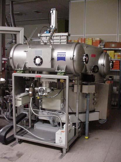
13 Fabrication processes used Processes Computer control polishing Differential Width profiling Stressed polishing Differential- profile coating Ion beam figuring (IBF) Smooth initial figuring deterministic correction with limited spatial resolution Partners APS optics group Zeiss General optics Crystal scientific Winlight


14 Figuring processes Lapping / Polishing Computer Controlled Stressed polishing Ion Beam Figuring Computer Controlled


15 Zeiss IBF capability Agreement in the sub-nm range!!! Zeiss D100 measurement face to the side Flat mirrors Bessy NOM Flat mirror for SPring8 Results: Zeiss D100 BESSY NOM Slope error 0.10 µrad rms 0.13 µrad rms Residual figure error 0.21 nm rms 0.56 nm rms 1.4 nm pv 2.3 nm pv Radius 60 km 61.2 km

16 APS- profile coating KB project R.Conley L.Assoufid 37 X 77 mm focal length mirrors


17 Dynamic KB : starting from existing designs ID19 low beta source at 150 m Energy 15 to 24 kev ID22 60 m high beta section slitted source Energy 17 kev

18 Shrinked design for dynamic KB Improvements Reduce focal length Mirror figure errors System vibrations Temperature induced drifts - feedback

 New commercial stitching")

19 Available metrology instrumentation for strong aspheres Need : 0.1 nm rms accuracy LTP accuracy being evaluated (Round Robin) New commercial stitching interferometers ADE phase shift, QED Evaluated by L. Assoufid at APS In situ Xray metrology (many other wavefront methods coming along)
 Focal plane")
 20")

20 pencil beam In situ metrology (wavefront derivative ) Focal plane deviations = 2 δα L δα L 80 mm FL multilayer (41 nm FWHM) 20 nanoradian rms slope precision figure error repeatabilty over 36 mm : 0.15 nm PV (0.03 nm rms)
21 Medium- long term perspectives Static multilayers mirrors preferred Substrate figuring : Zeiss, OSAKA U (JTEC), TINSLEY capability already at the nanometer level - Roughness to be confirmed Multilayers : Very steep gradients and phase correction feasability to be proven Metrology : Xray wavefront methods necessary and probably sufficient much beamtime needed. In situ figuring an attractive option
22 Pooling of synchrotron sources resources? Synchrotrons Challenge Establish a predictable secure procurement for all process operations keep control especially for metrology Market is small with respect to needed investments European FP7 initiative Europe -US collaborations Rely on what will be commercially available (OSAKA-JTEC)

 = 22 mm KB M = 9 D = 29 mm focus object z 1 z 2")

23 Application : projection microscopy Fresnel diffraction pattern - Spot size limited resolution Energy = 19 kev Magnification: (z 1 + z 2 )/z 1 = 3 Defocus: z 1 z 1 /(z 1 + z 2 ) = 22 mm KB M = 9 D = 29 mm focus object z 1 z 2 10 µm M = 18 D = 31 mm Defect of grating on a 100 nm scale revealed 2D detector 2 μm resolution P. Cloetens, O. Hignette


24 Phase Retrieval Possible single shot imaging with a priori information 10 μm 5 distances Neuron cell D = 45 mm Rel. Phase Map
 Al / Si alloy")


25 Application example : Magnified Tomography on ID19 (projection imaging) Al / Si alloy tomographic slice Si Pore Al 5 FeSi 75 μm Inside φ = 1 mm sample local tomography! E = 20.5 kev X-ray magnification ~ 80 (voxel size = 90 nm) R Mokso et al, submitted to Appl. Phys. Lett
26 Conclusions Reflective optics technology is now a serious candidate for < 10 nm nanofocusing Most needed technologies have been proven at a research level 1 nm goal needs huge (coordinated) efforts but not a total dream How and where to put resources to establish Full processes control Acknowledgements C.Morawe, P.Cloetens, R.Baker, A.Seifert, L Assoufid, R.Conley
27
28 Technologies developped at Short term KB nanofocusing projects system type coating focal length energy range spot size HXV(mm) kev (nanometers) dynamic multilayer 83 X X 50 dynamic multilayer 160 X X 200 dynamic multilayer 240 X X 40 dynamic Pt 80 X X 200 static Ni 60 X X 100 static Pt 37 X X 50
Characterisation of a novel super-polished bimorph mirror
 Characterisation of a novel super-polished bimorph mirror Kawal Sawhney 1, Simon Alcock 1, Hongchang Wang 1, John Sutter 1 and Riccardo Signorato 2 1 Diamond Light Source Ltd. UK 2 BASC, D-51429 Bergisch
Structure in out-of-focus beams of X-ray focusing mirrors: Causes and possible solutions. Fiona Rust Department of Physics, University of Bath
 Structure in out-of-focus beams of X-ray focusing mirrors: Causes and possible solutions John Sutter, Simon Alcock, Kawal Sawhney Diamond Light Source Ltd Fiona Rust Department of Physics, University of
Investigation of a Next Generation Piezo Bimorph Mirror
 Investigation of a Next Generation Piezo Bimorph Mirror Simon Alcock 1, Ioana Nistea 1, John Sutter 1, Kawal Sawhney 1, Jean-Jacques Fermé 2, Christophe Thellier 2, Luca Peverini 2 1 Optics & Metrology
Submicron focusing of hard X-rays with reflecting surfaces at the ESRF
 Submicron focusing of hard X-rays with reflecting surfaces at the ESRF Olivier Hignettel, Gerard Rostaing, Peter Cloetens, Amparo Rormneveaux, Wolfgang Ludwig, Andreas Freund European Synchrotron Radiation
Ion Beam Figuring precision optics for synchrotron radiation sources L. PEVERINI, J. J. FERME & C. du JEU
 www.thalesgroup.com Ion Beam Figuring precision optics for synchrotron radiation sources L. PEVERINI, J. J. FERME & C. du JEU Thales SESO S.A.S., Aix en Provence, 13593, France email: luca.peverini@fr.thalesgroup.com
Photon Diagnostics. FLASH User Workshop 08.
 Photon Diagnostics FLASH User Workshop 08 Kai.Tiedtke@desy.de Outline What kind of diagnostic tools do user need to make efficient use of FLASH? intensity (New GMD) beam position intensity profile on the
Nano Beam Position Monitor
 Introduction Transparent X-ray beam monitoring and imaging is a new enabling technology that will become the gold standard tool for beam characterisation at synchrotron radiation facilities. It allows
Breakout Session 3: Mirror Update. 2007/4/ /22 Peter M. Stefan LCLS Facility Advisory Committee (FAC) Meeting
 Meeting") Breakout Session 3: Mirror Update 2007/4/16-17 1/22 Peter M. Stefan LCLS Facility Advisory Committee (FAC) Meeting stefan@slac.stanford.edu Breakout Session 3: Mirror Update Overall Offset Mirror System
Breakout Session 3: Mirror Update 2007/4/16-17 1/22 Peter M. Stefan LCLS Facility Advisory Committee (FAC) Meeting stefan@slac.stanford.edu Breakout Session 3: Mirror Update Overall Offset Mirror System
Difrotec Product & Services. Ultra high accuracy interferometry & custom optical solutions
 Difrotec Product & Services Ultra high accuracy interferometry & custom optical solutions Content 1. Overview 2. Interferometer D7 3. Benefits 4. Measurements 5. Specifications 6. Applications 7. Cases
Correlation of mid-spatial features to image performance in aspheric mirrors
 Correlation of mid-spatial features to image performance in aspheric mirrors Flemming Tinker, Kai Xin Aperture Optical Sciences Inc., 27 Parson Ln. Unit G, Durham, CT 06422 ABSTRACT Modern techniques in
Wir schaffen Wissen heute für morgen
 Analyzing Wavefront and Spectrum of Hard X-ray Free-Electron Laser Radiation SLS (since 2001) Wir schaffen Wissen heute für morgen PSI: SLAC: SACLA: EuroXFEL: C. David, S. Rutishauser, P. Karvinen, I.
Performance of the SASE3 monochromator equipped with a provisional short grating. Variable line spacing grating specifications
 TECHNICAL REPORT Performance of the SASE monochromator equipped with a provisional short grating. Variable line spacing grating specifications N. Gerasimova for the X-Ray Optics and Beam Transport group
Optics for next generation light sources
 Optics for next generation light sources Anton Barty Centre for Free Electron Laser Science Hamburg, Germany Key issues Optical specifications Metrology (mirror surfaces) Metrology (wavefront, focal spot)
Hartmann wavefront sensing Beamline alignment
 Hartmann wavefront sensing Beamline alignment Guillaume Dovillaire SOS Trieste October 4th, 2016 G. Dovillaire M COM PPT 2016.01 GD 1 SOS Trieste October 4th, 2016 G. Dovillaire M COM PPT 2016.01 GD 2
First test experiments with FMB- Oxford direct drive DCM at the Sirius beamline of Synchrotron SOLEIL
 First test experiments with FMB- Oxford direct drive DCM at the Sirius beamline of Synchrotron SOLEIL Ciatto G., Moreno T., Aubert N., Feret P., Fontaine P. Synchrotron SOLEIL, L'Orme des Merisiers, Saint-Aubin,
State-of-the-art thin film X-ray optics for synchrotrons and FEL sources. Frank Hertlein Incoatec GmbH Geesthacht, Germany
 State-of-the-art thin film X-ray optics for synchrotrons and FEL sources Frank Hertlein Incoatec GmbH Geesthacht, Germany Incoatec: Innovative Coating Technologies Incoatec is founded with Bruker AXS in
Practical Flatness Tech Note
 Practical Flatness Tech Note Understanding Laser Dichroic Performance BrightLine laser dichroic beamsplitters set a new standard for super-resolution microscopy with λ/10 flatness per inch, P-V. We ll
New opportunities of freeform gratings using diamond machining
 New opportunities of freeform gratings using diamond machining Dispersing elements for Astronomy: new trends and possibilities 11/10/17 Cyril Bourgenot Ariadna Calcines Ray Sharples Plan of the talk Introduction
Carl Zeiss SMT. ACTOP 2008: Presentation Carl Zeiss Laser Optics. H. Thiess. LO-GOO Oct. 9, 2008
 Carl Zeiss SMT ACTOP 2008: Presentation Carl Zeiss Laser Optics H. Thiess LO-GOO Oct. 9, 2008 for public use Seite 1 Outline! Zeiss has decades of experience as optics manufacturer. Dedication to mirror
Challenges of Optics for High Repetition Rate XFEL Source
 Challenges of Optics for High Repetition Rate XFEL Source Liubov Samoylova, European XFEL GmbH ACTOP11, DIAMOND, April 5 th, 2011 2 European XFEL photon transport system - overview X-ray optics for XFEL:
Collector development with IR suppression and EUVL optics refurbishment at RIT
 Collector development with IR suppression and EUVL optics refurbishment at RIT Yuriy Platonov, Michael Kriese, Raymond Crucet, Yang Li, Vladimir Martynov, Licai Jiang, Jim Rodriguez Rigaku Innovative Technologies
EUV Micro-Exposure Tool (MET) for Near-Term Development Using a High NA Projection System
 for Near-Term Development Using a High NA Projection System") EUV Micro-Exposure Tool (MET) for Near-Term Development Using a High NA Projection System John S. Taylor, Donald Sweeney, Russell Hudyma Layton Hale, Todd Decker Lawrence Livermore National Laboratory
EUV Micro-Exposure Tool (MET) for Near-Term Development Using a High NA Projection System John S. Taylor, Donald Sweeney, Russell Hudyma Layton Hale, Todd Decker Lawrence Livermore National Laboratory
Bandpass Edge Dichroic Notch & More
 Edmund Optics BROCHURE Filters COPYRIGHT 217 EDMUND OPTICS, INC. ALL RIGHTS RESERVED 1/17 Bandpass Edge Dichroic Notch & More Contact us for a Stock or Custom Quote Today! USA: +1-856-547-3488 EUROPE:
EUV Multilayer Fabrication
 EUV Multilayer Fabrication Rigaku Innovative Technologies Inc. Yuriy Platonov, Michael Kriese, Jim Rodriguez ABSTRACT: In this poster, we review our use of tools & methods such as deposition flux simulation
The Design, Fabrication, and Application of Diamond Machined Null Lenses for Testing Generalized Aspheric Surfaces
 The Design, Fabrication, and Application of Diamond Machined Null Lenses for Testing Generalized Aspheric Surfaces James T. McCann OFC - Diamond Turning Division 69T Island Street, Keene New Hampshire
Physics 431 Final Exam Examples (3:00-5:00 pm 12/16/2009) TIME ALLOTTED: 120 MINUTES Name: Signature:
 TIME ALLOTTED: 120 MINUTES Name: Signature:") Physics 431 Final Exam Examples (3:00-5:00 pm 12/16/2009) TIME ALLOTTED: 120 MINUTES Name: PID: Signature: CLOSED BOOK. TWO 8 1/2 X 11 SHEET OF NOTES (double sided is allowed), AND SCIENTIFIC POCKET CALCULATOR
Physics 431 Final Exam Examples (3:00-5:00 pm 12/16/2009) TIME ALLOTTED: 120 MINUTES Name: PID: Signature: CLOSED BOOK. TWO 8 1/2 X 11 SHEET OF NOTES (double sided is allowed), AND SCIENTIFIC POCKET CALCULATOR
Steve O Dell
 Optics requirements for the Generation-X x-ray telescope Steve O Dell NASA Marshall Space Flight Center 2008.10.09-11 Authors Smithsonian Astrophysical Observatory (SAO) Roger Brissenden, Dan Schwartz,
Manufacturing Metrology Team
 The Team has a range of state-of-the-art equipment for the measurement of surface texture and form. We are happy to discuss potential measurement issues and collaborative research Manufacturing Metrology
Aspheric Lenses. Contact us for a Stock or Custom Quote Today! Edmund Optics BROCHURE
 Edmund Optics BROCHURE Aspheric Lenses products & capabilities Contact us for a Stock or Custom Quote Today! USA: +1-856-547-3488 EUROPE: +44 (0) 1904 788600 ASIA: +65 6273 6644 JAPAN: +81-3-3944-6210
Fiber Optic Communications
 Fiber Optic Communications ( Chapter 2: Optics Review ) presented by Prof. Kwang-Chun Ho 1 Section 2.4: Numerical Aperture Consider an optical receiver: where the diameter of photodetector surface area
Section 2: Lithography. Jaeger Chapter 2. EE143 Ali Javey Slide 5-1
 Section 2: Lithography Jaeger Chapter 2 EE143 Ali Javey Slide 5-1 The lithographic process EE143 Ali Javey Slide 5-2 Photolithographic Process (a) (b) (c) (d) (e) (f) (g) Substrate covered with silicon
APPLICATION NOTE
 THE PHYSICS BEHIND TAG OPTICS TECHNOLOGY AND THE MECHANISM OF ACTION OF APPLICATION NOTE 12-001 USING SOUND TO SHAPE LIGHT Page 1 of 6 Tutorial on How the TAG Lens Works This brief tutorial explains the
k λ NA Resolution of optical systems depends on the wavelength visible light λ = 500 nm Extreme ultra-violet and soft x-ray light λ = 1-50 nm
 Resolution of optical systems depends on the wavelength visible light λ = 500 nm Spatial Resolution = k λ NA EUV and SXR microscopy can potentially resolve full-field images with 10-100x smaller features
Test procedures Page: 1 of 5
 Test procedures Page: 1 of 5 1 Scope This part of document establishes uniform requirements for measuring the numerical aperture of optical fibre, thereby assisting in the inspection of fibres and cables
Lithography. 3 rd. lecture: introduction. Prof. Yosi Shacham-Diamand. Fall 2004
 Lithography 3 rd lecture: introduction Prof. Yosi Shacham-Diamand Fall 2004 1 List of content Fundamental principles Characteristics parameters Exposure systems 2 Fundamental principles Aerial Image Exposure
PHY 431 Homework Set #5 Due Nov. 20 at the start of class
 PHY 431 Homework Set #5 Due Nov. 0 at the start of class 1) Newton s rings (10%) The radius of curvature of the convex surface of a plano-convex lens is 30 cm. The lens is placed with its convex side down
Fabrication and alignment of 10X-Schwarzschild optics for F2X experiments
 Fabrication and alignment of 10X-Schwarzschild optics for F2X experiments a, Michael Shumway b,e, Lou Marchetti d, Donald Phillion c, Regina Soufli c, Manish Chandhok a, Michael Goldstein a, and Jeff Bokor
EE119 Introduction to Optical Engineering Spring 2003 Final Exam. Name:
 EE119 Introduction to Optical Engineering Spring 2003 Final Exam Name: SID: CLOSED BOOK. THREE 8 1/2 X 11 SHEETS OF NOTES, AND SCIENTIFIC POCKET CALCULATOR PERMITTED. TIME ALLOTTED: 180 MINUTES Fundamental
Experience of synchrotron sources and optics modelling at Diamond Light Source
 Experience of synchrotron sources and optics modelling at Diamond Light Source Lucia Alianelli Outline Microfocus MX beamline optics design (Principal Beamline Scientist G. Evans) Surface and interface
Modulation Transfer Function
 Modulation Transfer Function The Modulation Transfer Function (MTF) is a useful tool in system evaluation. t describes if, and how well, different spatial frequencies are transferred from object to image.
Design Description Document
 UNIVERSITY OF ROCHESTER Design Description Document Flat Output Backlit Strobe Dare Bodington, Changchen Chen, Nick Cirucci Customer: Engineers: Advisor committee: Sydor Instruments Dare Bodington, Changchen
Use of Computer Generated Holograms for Testing Aspheric Optics
 Use of Computer Generated Holograms for Testing Aspheric Optics James H. Burge and James C. Wyant Optical Sciences Center, University of Arizona, Tucson, AZ 85721 http://www.optics.arizona.edu/jcwyant,
NIST EUVL Metrology Programs
 NIST EUVL Metrology Programs S.Grantham, C. Tarrio, R.E. Vest, Y. Barad, S. Kulin, K. Liu and T.B. Lucatorto National Institute of Standards and Technology (NIST) Gaithersburg, MD USA L. Klebanoff and
Computer Generated Holograms for Optical Testing
 Computer Generated Holograms for Optical Testing Dr. Jim Burge Associate Professor Optical Sciences and Astronomy University of Arizona jburge@optics.arizona.edu 520-621-8182 Computer Generated Holograms
Research Article Fabrication and Performance Test of Fresnel Zone Plate with 35 nm Outermost Zone Width in Hard X-Ray Region
 Hindawi Publishing Corporation X-Ray Optics and Instrumentation Volume 2010, Article ID 824387, 6 pages doi:10.1155/2010/824387 Research Article Fabrication and Performance Test of Fresnel Zone Plate with
Sub-50 nm period patterns with EUV interference lithography
 Microelectronic Engineering 67 68 (2003) 56 62 www.elsevier.com/ locate/ mee Sub-50 nm period patterns with EUV interference lithography * a, a a b b b H.H. Solak, C. David, J. Gobrecht, V. Golovkina,
Technology Days GSFC Optics Technologies. Dr. Petar Arsenovic
 Technology Days 2011 GSFC Optics Technologies Dr. Petar Arsenovic Optics Capabilities Optical Design and Analysis Opto-mechanical Design and Fabrication Materials and Thin Films Component Development and
Cr, Co, Cu, Mo, Ag (others on request) Mean Reflectivity: R > 70%
 Mean Reflectivity: R > 70%") PARALLEL BEAM X-RAY OPTICS y Mirror length L Θ = f(x) b p/2 λ = 2d eff (x) sin Θ(x) eff x m Parallel beam width b=f(p,λ,l,,l,x m ) x Fabrication of high precision 6 mm parallel beam optics both on prefigured
PARALLEL BEAM X-RAY OPTICS y Mirror length L Θ = f(x) b p/2 λ = 2d eff (x) sin Θ(x) eff x m Parallel beam width b=f(p,λ,l,,l,x m ) x Fabrication of high precision 6 mm parallel beam optics both on prefigured
Application Note #548 AcuityXR Technology Significantly Enhances Lateral Resolution of White-Light Optical Profilers
 Application Note #548 AcuityXR Technology Significantly Enhances Lateral Resolution of White-Light Optical Profilers ContourGT with AcuityXR TM capability White light interferometry is firmly established
Optics for EUV Lithography
 Optics for EUV Lithography Dr. Sascha Migura, Carl Zeiss SMT GmbH, Oberkochen, Germany 2018 EUVL Workshop June 13 th, 2018 Berkeley, CA, USA The resolution of the optical system determines the minimum
On-line spectrometer for FEL radiation at
 On-line spectrometer for FEL radiation at FERMI@ELETTRA Fabio Frassetto 1, Luca Poletto 1, Daniele Cocco 2, Marco Zangrando 3 1 CNR/INFM Laboratory for Ultraviolet and X-Ray Optical Research & Department
Manufacturing, testing and alignment of Sentinel-2 MSI telescope mirrors
 Manufacturing, testing and alignment of Sentinel-2 MSI telescope mirrors P. Gloesener, F. Wolfs, F. Lemagne, C. Flebus AMOS Angleur, Belgium pierre.gloesener@amos.be P. Gloesener, F. Wolfs, F. Lemagne,
Characterization of Actinic Mask Blank Inspection for Improving Sensitivity
 Characterization of Actinic Mask Blank Inspection for Improving Sensitivity Yoshihiro Tezuka, Toshihiko Tanaka, Tsuneo Terasawa, Toshihisa Tomie * M-ASET, Tsukuba, Japan * M-ASRC, AIST, Tsukuba, Japan
Supplementary Information
 Supplementary Information Supplementary Figure 1. Modal simulation and frequency response of a high- frequency (75- khz) MEMS. a, Modal frequency of the device was simulated using Coventorware and shows
Femtosecond laser microfabrication in. Prof. Dr. Cleber R. Mendonca
 Femtosecond laser microfabrication in polymers Prof. Dr. Cleber R. Mendonca laser microfabrication focus laser beam on material s surface laser microfabrication laser microfabrication laser microfabrication
VUV-FEL User workshop, August 23-24, 2004
 Layout of the user facility Kai Tiedtke Kai Tiedtke, HASYLAB@ VUV-FEL User workshop, August 23-24, 2004 Kai.Tiedtke@desy.de Kai Tiedtke, HASYLAB@ Outline Photon beam transport Layout of the experimental
Diffractive optical elements and their potential role in high efficiency illuminators
 Diffractive optical elements and their potential role in high efficiency illuminators Patrick Naulleau Farhad Salmassi, Eric Gullikson, Erik Anderson Lawrence Berkeley National Laboratory Patrick Naulleau
X-ray generation by femtosecond laser pulses and its application to soft X-ray imaging microscope
 X-ray generation by femtosecond laser pulses and its application to soft X-ray imaging microscope Kenichi Ikeda 1, Hideyuki Kotaki 1 ' 2 and Kazuhisa Nakajima 1 ' 2 ' 3 1 Graduate University for Advanced
DCS laser for Thomson scattering diagnostic applications
 DCS laser for Thomson scattering diagnostic applications Authors Jason Zweiback 10/6/2015 jzweiback@logostech.net 1 Summary Motivation DCS laser Laser for Thomson scattering diagnostics 2 What is the Dynamic
3.0 Alignment Equipment and Diagnostic Tools:
 3.0 Alignment Equipment and Diagnostic Tools: Alignment equipment The alignment telescope and its use The laser autostigmatic cube (LACI) interferometer A pin -- and how to find the center of curvature
PROCEEDINGS OF SPIE. Structure in defocused beams of x- ray mirrors: causes and possible solutions
 PROCEEDINGS OF SPIE SPIEDigitalLibrary.org/conference-proceedings-of-spie Structure in defocused beams of x- ray mirrors: causes and possible solutions John P. Sutter, Simon G. Alcock, Fiona Rust, Hongchang
Status of the Electron Beam Transverse Diagnostics with Optical Diffraction Radiation at FLASH
 Status of the Electron Beam Transverse Diagnostics with Optical Diffraction Radiation at FLASH M. Castellano, E. Chiadroni, A. Cianchi, K. Honkavaara, G. Kube DESY FLASH Seminar Hamburg, 05/09/2006 Work
Spectrograph Lens Fabrication RFQ 22 Jan, 2003
 Spectrograph Lens Fabrication RFQ 22 Jan, 2003 1 Scope of Project This document describes the specifications for the fabrication of 18 optical elements to be used in the Prime Focus Imaging Spectrograph
Exam 3--PHYS 102--S10
 ame: Exam 3--PHYS 02--S0 Multiple Choice Identify the choice that best completes the statement or answers the question.. At an intersection of hospital hallways, a convex mirror is mounted high on a wall
Large Field of View, High Spatial Resolution, Surface Measurements
 Large Field of View, High Spatial Resolution, Surface Measurements James C. Wyant and Joanna Schmit WYKO Corporation, 2650 E. Elvira Road Tucson, Arizona 85706, USA jcwyant@wyko.com and jschmit@wyko.com
 http://goldberg.lbl.gov 1 To EUV or not to EUV? That is the question. Do we need EUV interferometry and EUV optical testing? 17 Things you need to know about perfecting EUV optics. 2 The main things you
Design of Photon Beamlines at the European XFEL
 Design of Photon Beamlines at the European XFEL Harald Sinn (THOCI1) FEL 2010 Malmö August 26, 2010 Construction progress at the European XFEL www.xfel.eu Experimental Hall in Schenefeld Injector building
CONFOCAL GRADED d-spacing MULTILAYER BEAM CONDITIONING OPTICS
 Copyright(C)JCPDS-International Centre for Diffraction Data 2000, Advances in X-ray Analysis, Vol.42 321 Copyright(C)JCPDS-International Centre for Diffraction Data 2000, Advances in X-ray Analysis, Vol.42
Photolithography II ( Part 2 )
") 1 Photolithography II ( Part 2 ) Chapter 14 : Semiconductor Manufacturing Technology by M. Quirk & J. Serda Saroj Kumar Patra, Department of Electronics and Telecommunication, Norwegian University of Science
1 Photolithography II ( Part 2 ) Chapter 14 : Semiconductor Manufacturing Technology by M. Quirk & J. Serda Saroj Kumar Patra, Department of Electronics and Telecommunication, Norwegian University of Science
Optical Components for Laser Applications. Günter Toesko - Laserseminar BLZ im Dezember
 Günter Toesko - Laserseminar BLZ im Dezember 2009 1 Aberrations An optical aberration is a distortion in the image formed by an optical system compared to the original. It can arise for a number of reasons
DEVELOPMENT OF A WAVELENGTH DISPERSIVE X-RAY FLUORESCENCE SPECTROMETER USING A MULTI-CAPILLARY X-RAY LENS FOR X-RAY DETECTION
 Copyright JCPDS - International Centre for Diffraction Data 2003, Advances in X-ray Analysis, Volume 46. 346 DEVELOPMENT OF A WAVELENGTH DISPERSIVE X-RAY FLUORESCENCE SPECTROMETER USING A MULTI-CAPILLARY
Recent Activities of the Actinic Mask Inspection using the EUV microscope at Center for EUVL
 Recent Activities of the Actinic Mask Inspection using the EUV microscope at Center for EUVL Takeo Watanabe, Tetsuo Harada, and Hiroo Kinoshita Center for EUVL, University of Hyogo Outline 1) EUV actinic
Product Information Version 1.0. ZEISS Xradia 810 Ultra Nanoscale X-ray Imaging at the Speed of Science
 Product Information Version 1.0 ZEISS Nanoscale X-ray Imaging at the Speed of Science Extending the Reach of 3D X-ray Imaging increases the throughput of nanoscale, three-dimensional X-ray imaging by up
Atomic Resolution Imaging with a sub-50 pm Electron Probe
 Atomic Resolution Imaging with a sub-50 pm Electron Probe Rolf Erni, Marta D. Rossell, Christian Kisielowski, Ulrich Dahmen National Center for Electron Microscopy, Lawrence Berkeley National Laboratory
Why is There a Black Dot when Defocus = 1λ?
 Why is There a Black Dot when Defocus = 1λ? W = W 020 = a 020 ρ 2 When a 020 = 1λ Sag of the wavefront at full aperture (ρ = 1) = 1λ Sag of the wavefront at ρ = 0.707 = 0.5λ Area of the pupil from ρ =
Fastest high definition Raman imaging. Fastest Laser Raman Microscope RAMAN
 Fastest high definition Raman imaging Fastest Laser Raman Microscope RAMAN - 11 www.nanophoton.jp Observation A New Generation in Raman Observation RAMAN-11 developed by Nanophoton was newly created by
Surface Finish Measurement Methods and Instrumentation
 125 years of innovation Surface Finish Measurement Methods and Instrumentation Contents Visual Inspection Surface Finish Comparison Plates Contact Gauges Inductive / Variable Reluctance (INTRA) Piezo Electric
The Formation of an Aerial Image, part 3
 T h e L i t h o g r a p h y T u t o r (July 1993) The Formation of an Aerial Image, part 3 Chris A. Mack, FINLE Technologies, Austin, Texas In the last two issues, we described how a projection system
Fabrication of Probes for High Resolution Optical Microscopy
 Fabrication of Probes for High Resolution Optical Microscopy Physics 564 Applied Optics Professor Andrès La Rosa David Logan May 27, 2010 Abstract Near Field Scanning Optical Microscopy (NSOM) is a technique
Introduction to Electron Microscopy
 Introduction to Electron Microscopy Prof. David Muller, dm24@cornell.edu Rm 274 Clark Hall, 255-4065 Ernst Ruska and Max Knoll built the first electron microscope in 1931 (Nobel Prize to Ruska in 1986)
GRINTECH GmbH. product information.
 GRINTECH GmbH product information www.grintech.de GRIN rod lenses Gradient index lenses for fiber coupling and beam shaping of laser diodes z l d s f Order example: GT-LFRL-100-025-50-CC (670) Design wavelength
Lecture 2: Geometrical Optics. Geometrical Approximation. Lenses. Mirrors. Optical Systems. Images and Pupils. Aberrations.
 Lecture 2: Geometrical Optics Outline 1 Geometrical Approximation 2 Lenses 3 Mirrors 4 Optical Systems 5 Images and Pupils 6 Aberrations Christoph U. Keller, Leiden Observatory, keller@strw.leidenuniv.nl
FIRST INDIRECT X-RAY IMAGING TESTS WITH AN 88-mm DIAMETER SINGLE CRYSTAL
 FERMILAB-CONF-16-641-AD-E ACCEPTED FIRST INDIRECT X-RAY IMAGING TESTS WITH AN 88-mm DIAMETER SINGLE CRYSTAL A.H. Lumpkin 1 and A.T. Macrander 2 1 Fermi National Accelerator Laboratory, Batavia, IL 60510
APPLICATION NOTE. Understanding the PV Specification. Introduction. Problems with PV
 APPLICATION NOTE Understanding the PV Specification Introduction An array of non-standard, arbitrary practices are frequently used in the optics industry to demonstrate conformance of a part to the traditional
Overview of performance and improvements to fixed exit double crystal monochromators at Diamond. Andrew Dent, Physical Science Coordinator, DLS
 Overview of performance and improvements to fixed exit double crystal monochromators at Diamond Andrew Dent, Physical Science Coordinator, DLS Overview Diffraction limit Geometric magnification Source
Inverted-COR: Inverted-Occultation Coronagraph for Solar Orbiter
 Inverted-COR: Inverted-Occultation Coronagraph for Solar Orbiter OATo Technical Report Nr. 119 Date 19-05-2009 by: Silvano Fineschi Release Date Sheet: 1 of 1 REV/ VER LEVEL DOCUMENT CHANGE RECORD DESCRIPTION
Sub-nanometer Interferometry Aspheric Mirror Fabrication
 UCRL-JC- 134763 PREPRINT Sub-nanometer Interferometry Aspheric Mirror Fabrication for G. E. Sommargren D. W. Phillion E. W. Campbell This paper was prepared for submittal to the 9th International Conference
EUV projection optics and active mirror development at SAGEM
 EUV projection optics and active mirror development at SAGEM R. Geyl,, M. Boutonne,, J.L. Carel,, J.F. Tanné, C. Voccia,, S. Chaillot,, J. Billet, Y. Poulard, X. Bozec SAGEM, Etablissement de St Pierre
An Off-Axis Hartmann Sensor for Measurement of Wavefront Distortion in Interferometric Detectors
 An Off-Axis Hartmann Sensor for Measurement of Wavefront Distortion in Interferometric Detectors Aidan Brooks, Peter Veitch, Jesper Munch Department of Physics, University of Adelaide Outline of Talk Discuss
Design and Manufacture of 8.4 m Primary Mirror Segments and Supports for the GMT
 Design and Manufacture of 8.4 m Primary Mirror Segments and Supports for the GMT Introduction The primary mirror for the Giant Magellan telescope is made up an 8.4 meter symmetric central segment surrounded
EUV and Soft X-Ray Optics
 David Attwood University of California, Berkeley Cheiron School September 2012 SPring-8 1 The short wavelength region of the electromagnetic spectrum n = 1 + i,
plasmonic nanoblock pair
 Nanostructured potential of optical trapping using a plasmonic nanoblock pair Yoshito Tanaka, Shogo Kaneda and Keiji Sasaki* Research Institute for Electronic Science, Hokkaido University, Sapporo 1-2,
Optical design of shining light through wall experiments
 Optical design of shining light through wall experiments Benno Willke Leibniz Universität Hannover (member of the ALPS collaboration) Vistas in Axion Physics: A Roadmap for Theoretical and Experimental
Nonintercepting Diagnostics for Transverse Beam Properties: from Rings to ERLs
 Nonintercepting Diagnostics for Transverse Beam Properties: from Rings to ERLs Alex H. Lumpkin Accelerator Operations Division Advanced Photon Source Presented at Jefferson National Accelerator Laboratory
Microscope anatomy, image formation and resolution
 Microscope anatomy, image formation and resolution Ian Dobbie Buy this book for your lab: D.B. Murphy, "Fundamentals of light microscopy and electronic imaging", ISBN 0-471-25391-X Visit these websites:
Point Autofocus Probe Surface Texture Measuring Instrument. PF-60 technical report
 Point Autofocus Probe Surface Texture Measuring Instrument PF-60 technical report ISO approved Mitaka measuring method for areal surface texture (ISO 25178-605) Document No, Title Published ISO 25178-6
Aberrations and adaptive optics for biomedical microscopes
 Aberrations and adaptive optics for biomedical microscopes Martin Booth Department of Engineering Science And Centre for Neural Circuits and Behaviour University of Oxford Outline Rays, wave fronts and
Synthesis of projection lithography for low k1 via interferometry
 Synthesis of projection lithography for low k1 via interferometry Frank Cropanese *, Anatoly Bourov, Yongfa Fan, Andrew Estroff, Lena Zavyalova, Bruce W. Smith Center for Nanolithography Research, Rochester
06SurfaceQuality.nb Optics James C. Wyant (2012) 1
 1") 06SurfaceQuality.nb Optics 513 - James C. Wyant (2012) 1 Surface Quality SQ-1 a) How is surface profile data obtained using the FECO interferometer? Your explanation should include diagrams with the appropriate
06SurfaceQuality.nb Optics 513 - James C. Wyant (2012) 1 Surface Quality SQ-1 a) How is surface profile data obtained using the FECO interferometer? Your explanation should include diagrams with the appropriate
Spatial resolution. Spatial resolution
 11/05/00 Refraction Compound refractive lenses (concave) Snigirev et al, NATURE 199 patents: Tomie 1995 x-rays: n = 1 - δ - i β < 1 www.accel.de Chromatic lenses Prod.: Lengeler @RWTH Aachen, D need of