imec image sensors and vision systems
|
|
|
- Chloe Patrick
- 6 years ago
- Views:
Transcription

1 imec image sensors and vision systems


2 IMEC FOCUS: SPECIALTY IMAGING Design innovation Process Technologies Machine Vision Industrial Instrumentation Key features: High speed Low power Low noise High-end transports, security & surveillance microscopy Life-Science & Medical Imaging High QE Radiation Hard + Space, Physics & Scientific Non- Visible sensing Spectral sensing 2


")
 Custom")


3 IMEC - POSITIONING 200mm / 8 wafer fab 0.13um CMOS based process imaging R&D imager DESIGN CMOS imager MANUFACTURING imager PACKAGING/TEST Dedicated team with 3-shift operations Qualification (characterization, reliability, testing) Optical package, assembly & test Vision system design (HW/SW) Co-design (of specific pixels, analog, digital blocks) Custom circuit calibration, simulation, verification Radiation-hard designs INFRASTRUCTURE DESIGN ENVIRONMENT PROCESS TECHNOLOGIES Specific substrate Pixels (3T, 4T, trench isolation, embedded CCD pixels in CMOS) BSI Backside illumination Hyperspectral filters Special ARCs (CMOS compatible) Stitching / Butting capabilities for large area imagers Radiation-hard coatings Micro-bumping, 3D integration with TSV interconnects
4 IMEC IMAGE SENSORS & VISION SYSTEMS Line scan imager Cell sorter Microscopy imaging X-Ray Electron detectors UV / EUV imager & detectors HYPER SPECTRAL VISION SYSTEM Snapshot imager Evaluation System LENS FREE VISION SYSTEM Industrial NON VISIBLE IMAGE SENSORS NIR Backside illumination (BSI) STEREO VISION VISION SYSTEM 3D stereo -vision ORGANIC IMAGE SENSORS LOW NOISE HIGH SPEED HIGH QE IMAGE SENSORS embedded CCD (in CMOS) 4


5 IMEC BACKSIDE ILLUMINATION PLATFORM Quantum Efficiency QE Higher fill factor Better sensitivity in visible Ultraviolet NIR detection Based on IMEC s 0.13 micron Cu BEOL process: Proprietary FSI process with support for variable pixel size 1 Advanced bonding, thinning, passivation modules 0.9 Dedicated ARCs developments Quantum Yield taken into account Wavelength (nm) Wavelength (nm)
6 IMEC ECCD PLATFORM Extra module in imec 130nm CMOS/CIS technology Narrow gap, single poly electrodes Customizable, BSI compatible CCD device Fully CMOS compatible for ROIC design Excellent charge transfer efficiency (CTE): > % First TDI imager available CCD pixels PG-1 PG-2 PG-3 PG-4 TX CMOS read-out VDD RST VDD SF RS Out read-out sequence FD (TDI = time delay integration)
 Broadband or Selectively sensitive to UV-VIS-NIR light OPD technologies @ imec")

7 ORGANIC PHOTO-DETECTORS (OPD) Hyperspectral OPD imaging Many patterned OPDs Ultra-thin layers of organic materials (<100 nm) Deposited from solution or evaporated High absorption coefficient (compared to Si) Broadband or Selectively sensitive to UV-VIS-NIR light OPD imec High-sensitivity imaging 1. OPD on CMOS backplane readout 2. OPD on flexible backplane readout Three patterned OPDs Near-Infrared enhancement Color filters on Si +NIR OPD pixels Enhanced performance (crosstalk, resolution, dynamic range, bandwidth) New functionalities (thin, light-weight, large-area)
8 IMEC IMAGE SENSORS & VISION SYSTEMS Line scan imager Cell sorter Microscopy imaging X-Ray Electron detectors UV / EUV imager & detectors HYPER SPECTRAL VISION SYSTEM Snapshot imager Evaluation System LENS FREE VISION SYSTEM Industrial NON VISIBLE IMAGE SENSORS NIR Backside illumination (BSI) STEREO VISION VISION SYSTEM 3D stereo -vision ORGANIC IMAGE SENSORS LOW NOISE HIGH SPEED HIGH QE IMAGE SENSORS embedded CCD (in CMOS)


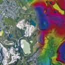
9 HYPERSPECTRAL IMAGING Improves vision and discrimination power by using spectral signature information of surface material / object being captured n 1 2


10 SPECTRAL IMAGING OPENS A NEW DIMENSION Spectrometer Color camera Hyperspectral camera λ y x B G R λ1,2,3 λ1..n y x Accurate spectral analysis of one spatial pixel only Seeing RGB colors of one image only spectral signature of images reveals objects chemical surface composition


11 CONVERGENCE OF IMAGING & SPECTROSCOPY High discrimination power SPECTROSCOPY Single point with highest spectral resolution IMEC approach: spectral filters integrated on pixels Bayer pattern OR Tiled pattern OR Wedge pattern IMAGING SPECTROSCOPY RGB filters on multiple pixels High speed, high spatial resolution IMAGING

12 IMEC APPROACH: FABRY-PEROT SPECTRAL FILTERS ON TOP OF IMAGE SENSOR L θ θ Wavelength selection depends on cavity length L k 2nLcos Tx (%) Narrow-band & high transmission efficiencies spectral filters Different cavity heights = different spectral wavelengths captured! FWHM ~ 5-20nm


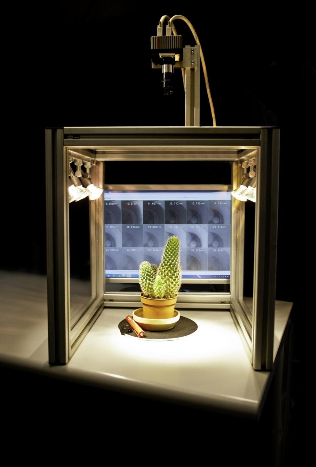
13 SPECTRAL FILTERS APPLIED TO COMMERCIAL SENSOR WAFERS USING SEMICONDUCTOR WAFER PROCESSING Example of IMEC hyperspectral filter structures processed at wafer-level on top of commercial CMOS image sensor wafer (here on CMOSIS s CMV2000 & CMV4000 sensors)


14 IMEC HYPERSPECTRAL TECHNOLOGY USP Filter response Filters fully integrated on pixels and CMOS compatible - Extra post-processing step in standard image sensor production - Small feature sizes OK as based on standard lithography - No assembly, no alignment nor stray light issues Optical filters & imager can be customized to match with final application requirements - Number of filters, central wavelength, FWHM - Possibility to fill sensor with ONLY selected bands of interest (not restricted to continuous wavelength, or range or specific line arrangement) FWHM 1 2 n Continuous Line-scan Custom Line-scan Snapshot Tiled Snapshot Bayer Mosaic All tunable: results in high speed, compact & cost-effective hyperspectral solution!
 NO SCAN = real-time HSI data-cubes acquisition Spatial vs.")

")
15 SUMMARY OF HSI SENSOR DESIGN APPROACHES Line-scan wedge design Snapshot tiled area design Snapshot mosaic per-pixel design Or Or SCANNING movement needed Highest spatial & spectral resolution achievable (e.g. 100 spectral band images of 4MPx resolution today) NO SCAN = real-time HSI data-cubes acquisition Spatial vs. Spectral resolution trade-off (e.g. 32 band images of 256x256 resolution today) Optical duplicator needed (e.g. 32 lens-array today) NO SCAN = real-time HSI data-cubes acquisition Spatial vs. Spectral resolution trade-off (e.g. 16 band images of 512x272 resolution today) Potential resolution reconstruction increase by de-mosaicing algorithms NO optical duplicator needed (standard lens camera integration)
16 1088 pixels LINE-SCAN SENSOR DESIGN (GEN 1) CMOSIS CMV pixels 8 pixels 1000nm 8 pixels 996nm 8 pixels 992nm spectral bands of 2048x8 spatial pixels each 8 pixels 608nm 8 pixels 604nm 8 pixels 600nm Key specifications - Spectral resolution: 100 bands in nm with 4nm incremental steps - FWHM: ~ 15nm - Spatial resolution: 2048 pixels x length of scan - Speed: up to 340 fps (full sensor frame)
17 1088 pixels LINE-SCAN SENSOR DESIGN (GEN 2) CMOSIS CMV pixels 900nm 8 pixels 895nm 8 pixels 890nm spectral bands of 2048x8 spatial pixels each 2048 pixels 8 pixels 480nm 8 pixels 475nm 8 pixels 470nm Key specifications - Spectral resolution: 100 bands in nm with 5nm incremental steps - FWHM: ~ 15nm - Spatial resolution: 2048 pixels x length of scan - Speed: up to 340 fps (full sensor frame) Sensor available Q4-2014

 - FWHM: ~ 15nm - Spatial resolution: 256x256 for each spectral band - Speed: up to 340 data-cubes / s (max")
18 1088 pixels SNAPSHOT TILED SENSOR DESIGN 1 tile = 256x256 pixels CMOSIS CMV nm 582nm 775nm 761nm 841nm 874nm 630nm 899nm 820nm 833nm 725nm 688nm 801nm 865nm 920nm 885nm 700nm 715nm 644nm 595nm 895nm 911nm 606nm 905nm 676nm 856nm 656nm 621nm 557nm 907nm 737nm 600nm 2048 pixels Key specifications - Spectral resolution: 32bands in nm with 12nm incremental steps (optical duplicator needed) - FWHM: ~ 15nm - Spatial resolution: 256x256 for each spectral band - Speed: up to 340 data-cubes / s (max sensor limit)
 = 16bands in 465-630nm with ~11nm incremental steps - FWHM: ~ 15nm - Spatial")
19 1088 pixels SNAPSHOT MOSAIC SENSOR DESIGN (GEN1) 4x4 mosaic = 16 bands CMOSIS CMV nm 546 nm 586 nm 630 nm 474 nm 534 nm 578 nm 624 nm 485 nm 522 nm 562 nm 608 nm 2x1mosaics 496 nm 510 nm 548 nm 600 nm 6x6 mosaic 4x4 mosaic Key specifications 2048 pixels - Spectral resolution: 4x4 mosaic (1filter / pixel) = 16bands in nm with ~11nm incremental steps - FWHM: ~ 15nm - Spatial resolution: from 512x272 (per band) up to 2Mpx (per band) depending on de-mosaicing algorithm - Speed: up to 340 data-cubes / s (max sensor limit) - No optical duplicator element needed = simplified camera design
20 IMEC HYPERSPECTRAL FILTER TECHNOLOGY ROADMAP Snapshot Mosaic per-pixel Integration of Panchromatic + spectral filters 4x4 Mosaic GEN nm (16bands) Mixing Panchromatic + HSI filters 4x4 Mosaic nm GEN2 5x5 Mosaic nm GEN3 Mixing RGB CF + HSI filters Snapshot Tile HSI Tiled filter pattern GEN nm (32bands) HSI Tiled filter pattern nm Line-scan Wedge HSI Wedge filter pattern GEN nm (100bands) HSI Wedge filter pattern GEN nm (100bands) HSI Wedge filter pattern nm (100bands)

21


 350 400 450 500 550")


22 WHERE IS THE KEY SPECTRAL INFORMATION? Color measurements m Chlorophyll absorption / vegetation reflectance nm Water absorption 970nm +1450nm +1850nm Fluorescence imaging peaks m Oxygenation in blood m CH4 2300nm CO2 2100nm +3500nm nm (nm) m Skin tones / tissue chromophores m Hydrocarbon organic compounds (Ethanol, Benzene, Aromatics, ETBE, MTBE, Toluene...) 1700nm -1900nm 2300nm -2400nm Minerals mapping PVC / plastic recycling


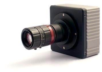
23 COMMERCIAL CAMERA PARTNERS FOR HSI SENSOR INTEGRATION High speed camera Cameralink or CoaXPress interface Compact optical design with ZIFF socket to swap different HSI sensors Robust camera implementation for use in industrial, medical and global security Intelligent D3 camera platform Giga/Ethernet interface Focus on remote sensing, UAV & machine vision Smart camera Giga/Ethernet interface Reprogrammable FPGA pre-processing hypercube data inside camera Focus on industrial & machine vision Intelligent vision module Giga/Ethernet interface Motorized optics Embedded HSI data processing include storage Multi-camera head option USB 3.0 vision camera High-speed USB3.0 camera interface Ultra compact camera: 26.4 x 26.4 x 21.2 mm 27grams weight only! Handheld mobile device First proof-of-concept of IMEC s HSI sensors integration to mobile Android OS open platform USB2.0 interface


24 NEW PARTNERSHIP WITH XIMEA WORLD S SMALLEST INDUSTRIAL USB3 VISION AND HYPERSPECTRAL IMAGING CAMERA 465nm 510nm 548nm 600nm 474nm 522nm 562nm 608nm 485nm 534nm 578nm 624nm 496nm 546nm 586nm 630nm

25 Precision farming: Detection, diagnosis and control of plant diseases environmental stresses weeds and invasive species Growth monitoring Treatment optimisation Yield prediction RGB Hyperspectral


26 KEY DRIVING HYPERSPECTRAL INDUSTRIAL APPLICATIONS Remote sensing UAV/drones & nano-satelites for: Precision agriculture Environment monitoring Terrestrial / maritime earth observation Life-science / spectroscopy instrumentation Imaging spectroscopy analyzers DNA sequencers / flow cytometers Water monitoring analyzers Blood / urine analyzers Machine vision / Optical sorting Food sorting / quality grading Pharmaceutical defect inspection Industrial inspection (plastic, ceramic, glass, etc...) Robotic machine vision Mining / Mineralogy Print quality inspection Automotive & Transport Night vision systems Fuel monitoring systems Medical imaging Security / Surveillance Surgery-guided imaging Fluorescence microscopy Endoscopy Ophthalmology / retina imaging Wounds imaging Industrial gas leaks monitoring Intrusion detection / authentication Rescue Forensics


 Source L")


27 THERE ARE ALSO HANDHELD & CONSUMER APPLICATIONS! Food quality grading (e.g. sugar content in fruits, monitoring calorie intake, etc...) Cosmetic / Skin tone measurement (e.g. make-up advice, etc...) Source L OREAL Skin-care / personalized medicine (e.g. melanoma, vitiligo, diabetic ulcers, wound care...) True Colors (e.g. white balancing, calibration, ALS ) Anti counterfeiting spectral tag readers


28 IMEC HYPERSPECTRAL IMAGING ROADMAP Establishing partnerships with multiple camera partners Public demo Multispectral video 32 bands at 180 fps Public demo nm 100 spectral bands HSI Evaluation Systems HSI Snapshot imager HSI cameras New filter architectures Per-pixel mosaic design nm additional coverage nm full coverage Explore new concepts IR filters bands coverage (1-2.5um) Microscopy set-up Medical applications HSI Line-scan imager Full system with imec sensor + camera + HSI software
29 IMEC IMAGE SENSORS & VISION SYSTEMS Line scan imager Cell sorter Microscopy imaging X-Ray Electron detectors UV / EUV imager & detectors HYPER SPECTRAL VISION SYSTEM Snapshot imager Evaluation System LENS FREE VISION SYSTEM Industrial (MEMS based) NON VISIBLE IMAGE SENSORS NIR Backside illumination (BSI) STEREO VISION VISION SYSTEM 3D stereo -vision ORGANIC IMAGE SENSORS LOW NOISE HIGH SPEED HIGH QE IMAGE SENSORS embedded CCD (in CMOS)

 = miniaturized + low cost - Large field-of-view ( FOV > 100mm 2 depending on imager size) - High resolution (e.g. < 1.")
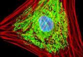
30 LENS-FREE IMAGING VS. CONVENTIONAL MICROSCOPE: COMPACT, COST-EFFECTIVE, SCALABLE MATCHED TO APPLICATION! Traditional phase-contrast microscope - Bulky, optically and mechanically complex - Expensive high quality lenses required - Limited field of view at high resolution - Focusing by mechanical movement of optical elements Not suitable for large-area inspection, because of limited single microscope throughput and difficulty to put many in parallel Lens-Free Imaging (LFI) microscope - No lenses (minimal optical and mech. components) = miniaturized + low cost - Large field-of-view ( FOV > 100mm 2 depending on imager size) - High resolution (e.g. < 1.4µm capable) - Auto-focus is part of post-processing steps achieved at software level Removing lenses enables very compact and cost-effective system and integrated approach can be massively parallelized for large area inspection


31 EXAMPLE OF LENS-FREE IMAGING LARGE FIELD OF VIEW WITH HIGH RESOLUTION High level of detail (1.23um resolution) Large field of view = imager size ~ 6.4mm x 4.6mm


32 RESOLUTION EXCEEDS LARGE FOV MICROSCOPE IMAGING Large FOV LFI Microscopy 4x 100 µm
33 IMEC IMAGE SENSORS & VISION SYSTEMS Line scan imager Cell sorter Microscopy imaging X-Ray Electron detectors UV / EUV imager & detectors HYPER SPECTRAL VISION SYSTEM Snapshot imager Evaluation System LENS FREE VISION SYSTEM Industrial (MEMS based) NON VISIBLE IMAGE SENSORS NIR Backside illumination (BSI) STEREO VISION VISION SYSTEM 3D stereo -vision ORGANIC IMAGE SENSORS LOW NOISE HIGH SPEED HIGH QE IMAGE SENSORS embedded CCD (in CMOS)
 Object shape: Object shape integrity Lighting")

34 STEREOMATCHING DEPTH MAP GENERATION Compact form factor: CMOS sensor-based Latency: Fairly low latency (<1 frame) Object shape: Object shape integrity Lighting condition: Good for indoor/outdoor Background: Can deal with complex background Distance range: Very long (vs. active TOF with IR) Reliability: with supplement Confidence index
35
36 KEY SPECIFICATION ITEMS Spec. Item Number Remark Disparity Levels 128 (1/8) 64 and 32 are also supported ; 1/8 fractional disparity Frame Rate & Resolution 60FPS 1280x x1080 is also supported Pixel Clock Rate (MHz) 100 MHz For TSMC 90nm library, using Cadence RC synthesis FPGA Clock Rate (MHz) 74 MHz For side-by-side 1920x1080 MDE/s MDE/s = (Frame Rate) * (Resolution) * (Dispartiy) / 10E6 Power Consumption 82.4 mw For using Cadence RC vectorless power analysis Extra DRAM size NO No frame buffer required Ambient Light > 100 Lux Depends also on camera SNR Rectification Real-time Through software register setting Gate Count 610 K MIN TYPICAL : 610k (for logic, VGA 60FPS, 128 level ) Latency <0.2 frame rate
37 IMEC IMAGE SENSORS & VISION SYSTEMS Line scan imager Cell sorter Microscopy imaging X-Ray Electron detectors UV / EUV imager & detectors HYPER SPECTRAL VISION SYSTEM Snapshot imager Evaluation System LENS FREE VISION SYSTEM Industrial (MEMS based) NON VISIBLE IMAGE SENSORS NIR Backside illumination (BSI) STEREO VISION VISION SYSTEM 3D stereo -vision ORGANIC IMAGE SENSORS LOW NOISE HIGH SPEED HIGH QE IMAGE SENSORS embedded CCD (in CMOS)
38 Thank you!
CMOS BASED HYPERSPECTRAL IMAGING FOR COMPACT / LOW-COST / HIGH-VOLUME IMAGING SPECTROSCOPY. SPIE Baltimore - April 2016
 CMOS BASED HYPERSPECTRAL IMAGING FOR COMPACT / LOW-COST / HIGH-VOLUME IMAGING SPECTROSCOPY SPIE Baltimore - April 2016 WHY DO WE NEED HYPERSPECTRAL IMAGING? to improve vision and discrimination power...
Miniaturized hyperspectral imaging cameras
 Fraunhofer IOSB KCM SpectroNet Collaboration Forum 2015 Miniaturized hyperspectral imaging cameras 1 Hyper spectral imaging (HSI) 2 HSI sensor types from imec filter layouts Linescan Snapshot Mosaic Snapshot
Hyperspectral imaging (HSI) goes embedded All rights reserved Max Larin, 1
 goes embedded All rights reserved Max Larin, 1") Hyperspectral imaging (HSI) goes embedded 2015 All rights reserved Max Larin, max.larin@ximea.com 1 Hyperspectral Imaging (HSI) goes embedded Seeing the invisible with Miniature intelligent HSI Cameras
Hyperspectral imaging (HSI) goes embedded 2015 All rights reserved Max Larin, max.larin@ximea.com 1 Hyperspectral Imaging (HSI) goes embedded Seeing the invisible with Miniature intelligent HSI Cameras
Interference metal/dielectric filters integrated on CMOS image sensors SEMICON Europa, 7-8 October 2014
 Interference metal/dielectric filters integrated on CMOS image sensors SEMICON Europa, 7-8 October 2014 laurent.frey@cea.fr Outline Spectral filtering applications Consumer Multispectral Prior art Organic
Image sensor combining the best of different worlds
 Image sensors and vision systems Image sensor combining the best of different worlds First multispectral time-delay-and-integration (TDI) image sensor based on CCD-in-CMOS technology. Introduction Jonathan
Imaging with hyperspectral sensors: the right design for your application
 Imaging with hyperspectral sensors: the right design for your application Frederik Schönebeck Framos GmbH f.schoenebeck@framos.com June 29, 2017 Abstract In many vision applications the relevant information
Jan Bogaerts imec
 imec 2007 1 Radiometric Performance Enhancement of APS 3 rd Microelectronic Presentation Days, Estec, March 7-8, 2007 Outline Introduction Backside illuminated APS detector Approach CMOS APS (readout)
More Imaging Luc De Mey - CEO - CMOSIS SA
 More Imaging Luc De Mey - CEO - CMOSIS SA Annual Review / June 28, 2011 More Imaging CMOSIS: Vision & Mission CMOSIS s Business Concept On-Going R&D: More Imaging CMOSIS s Vision Image capture is a key
The chemical camera for your microscope
 The chemical camera for your microscope» High Performance Hyper Spectral Imaging» Data Sheet The HSI VIS/NIR camera system is an integrated laboratory device for the combined color and chemical analysis.
INNOVATIVE SPECTRAL IMAGING
 INNOVATIVE SPECTRAL IMAGING food inspection precision agriculture remote sensing defense & reconnaissance advanced machine vision product overview INNOVATIVE SPECTRAL IMAGING Innovative diffractive optics
Short Wave Infrared (SWIR) Imaging In Machine Vision
 Imaging In Machine Vision") Short Wave Infrared (SWIR) Imaging In Machine Vision Princeton Infrared Technologies, Inc. Martin H. Ettenberg, Ph. D. President martin.ettenberg@princetonirtech.com Ph: +01 609 917 3380 Booth Hall 1 J12
Short Wave Infrared (SWIR) Imaging In Machine Vision Princeton Infrared Technologies, Inc. Martin H. Ettenberg, Ph. D. President martin.ettenberg@princetonirtech.com Ph: +01 609 917 3380 Booth Hall 1 J12
Hyperspectral Systems: Recent Developments and Low Cost Sensors. 56th Photogrammetric Week in Stuttgart, September 11 to September 15, 2017
 Hyperspectral Systems: Recent Developments and Low Cost Sensors 56th Photogrammetric Week in Stuttgart, September 11 to September 15, 2017 Ralf Reulke Humboldt-Universität zu Berlin Institut für Informatik,
e2v Launches New Onyx 1.3M for Premium Performance in Low Light Conditions
 e2v Launches New Onyx 1.3M for Premium Performance in Low Light Conditions e2v s Onyx family of image sensors is designed for the most demanding outdoor camera and industrial machine vision applications,
Spectral and Polarization Configuration Guide for MS Series 3-CCD Cameras
 Spectral and Polarization Configuration Guide for MS Series 3-CCD Cameras Geospatial Systems, Inc (GSI) MS 3100/4100 Series 3-CCD cameras utilize a color-separating prism to split broadband light entering
WHITE PAPER MINIATURIZED HYPERSPECTRAL CAMERA FOR THE INFRARED MOLECULAR FINGERPRINT REGION
 WHITE PAPER MINIATURIZED HYPERSPECTRAL CAMERA FOR THE INFRARED MOLECULAR FINGERPRINT REGION Denis Dufour, David Béland, Hélène Spisser, Loïc Le Noc, Francis Picard, Patrice Topart January 2018 Low-cost
HSI CAMERAS FOR FOOD SAFETY AND FRAUD DETECTION
 1 Max Larin, XIMEA HSI CAMERAS FOR FOOD SAFETY AND FRAUD DETECTION 2 What are we talking about? Food safety risks: Common for all countries, with some differences though 1/3 of population in developed
BaySpec SuperGamut OEM
 BaySpec SuperGamut OEM Spectrographs & Spectrometers RUGGED SOLID STATE HIGH RESOLUTION OPTIMIZED COOLING COST EFFECTIVE HIGH THROUGHPUT www.bayspec.com Specifications Model UV-NIR VIS-NIR NIR 900-1700nm
SPECIM, SPECTRAL IMAGING LTD.
 HSI IN A NUTSHELL SPECIM, SPECTRAL IMAGING LTD. World leading manufacturer and suppplier for hyperspectral imaging technology and solutions Hundreds of customers worldwide. Distributor and integrator network
MEMS Spectroscopy Overview
 MEMS Spectroscopy Overview LIVING IN A SENSORY WORLD Everyday, and in so many ways, we circulate in a world of sensors. We do so mainly without knowing it. MEMS, sensors and the Internet of Things (IoT)
746A27 Remote Sensing and GIS. Multi spectral, thermal and hyper spectral sensing and usage
 746A27 Remote Sensing and GIS Lecture 3 Multi spectral, thermal and hyper spectral sensing and usage Chandan Roy Guest Lecturer Department of Computer and Information Science Linköping University Multi
brief history of photography foveon X3 imager technology description
 brief history of photography foveon X3 imager technology description imaging technology 30,000 BC chauvet-pont-d arc pinhole camera principle first described by Aristotle fourth century B.C. oldest known
Moving from biomedical to industrial applications: OCT Enables Hi-Res ND Depth Analysis
 Moving from biomedical to industrial applications: OCT Enables Hi-Res ND Depth Analysis Patrick Merken a,c, Hervé Copin a, Gunay Yurtsever b, Bob Grietens a a Xenics NV, Leuven, Belgium b UGENT, Ghent,
SOLAR CELL INSPECTION WITH RAPTOR PHOTONICS OWL (SWIR) AND FALCON (EMCCD)
 AND FALCON (EMCCD)") Technical Note Solar Cell Inspection SOLAR CELL INSPECTION WITH RAPTOR PHOTONICS OWL (SWIR) AND FALCON (EMCCD) August 2012, Northern Ireland Solar cell inspection relies on imaging the photoluminescence
Technical Note Solar Cell Inspection SOLAR CELL INSPECTION WITH RAPTOR PHOTONICS OWL (SWIR) AND FALCON (EMCCD) August 2012, Northern Ireland Solar cell inspection relies on imaging the photoluminescence
Time Delay Integration (TDI), The Answer to Demands for Increasing Frame Rate/Sensitivity? Craige Palmer Assistant Sales Manager
, The Answer to Demands for Increasing Frame Rate/Sensitivity? Craige Palmer Assistant Sales Manager") Time Delay Integration (TDI), The Answer to Demands for Increasing Frame Rate/Sensitivity? Craige Palmer Assistant Sales Manager Laser Scanning Microscope High Speed Gated PMT Module High Speed Gating
Time Delay Integration (TDI), The Answer to Demands for Increasing Frame Rate/Sensitivity? Craige Palmer Assistant Sales Manager Laser Scanning Microscope High Speed Gated PMT Module High Speed Gating
450mm and Moore s Law Advanced Packaging Challenges and the Impact of 3D
 450mm and Moore s Law Advanced Packaging Challenges and the Impact of 3D Doug Anberg VP, Technical Marketing Ultratech SOKUDO Lithography Breakfast Forum July 10, 2013 Agenda Next Generation Technology
Specim. Making spectral imaging possible
 Specim Making spectral imaging possible SPECIM, Spectral Imaging Ltd. World leading manufacturer and suppplier for hyperspectral imaging technology and solutions Hundreds of customers worldwide. Distributor
MICRO SPECTRAL SCANNER
 MICRO SPECTRAL SCANNER The OEM μspectral Scanner is a components kit that can be interfaced to existing microscope ready to accept cameras with Cmount to obtain an hyper-spectral imaging system. With OEM
GUIDE TO SELECTING HYPERSPECTRAL INSTRUMENTS
 GUIDE TO SELECTING HYPERSPECTRAL INSTRUMENTS Safe Non-contact Non-destructive Applicable to many biological, chemical and physical problems Hyperspectral imaging (HSI) is finally gaining the momentum that
Challenges in Imaging, Sensors, and Signal Processing
 Challenges in Imaging, Sensors, and Signal Processing Raymond Balcerak MTO Technology Symposium March 5-7, 2007 1 Report Documentation Page Form Approved OMB No. 0704-0188 Public reporting burden for the
sensors & systems Imagine future imaging... Leti, technology research institute Contact:
 Imaging sensors & systems Imagine future imaging... Leti, technology research institute Contact: leti.contact@cea.fr From consumer markets to high-end applications smart home IR array for human activity
Tunable wideband infrared detector array for global space awareness
 Tunable wideband infrared detector array for global space awareness Jonathan R. Andrews 1, Sergio R. Restaino 1, Scott W. Teare 2, Sanjay Krishna 3, Mike Lenz 3, J.S. Brown 3, S.J. Lee 3, Christopher C.
ULS24 is built on 0.18um CMOS process at a world-leader specialty semiconductor foundry. LDO. 3.3v/1.8v 30mW. SPI uc (32-bit) 12 Mhz OSC
 12 Mhz OSC") Product overview The Anitoa ULS24 is an ultra-low-light CMOS image sensor. Its low cost, small form factor and high level of integration make it optimally suited for use in a portable device in medical,
Product overview The Anitoa ULS24 is an ultra-low-light CMOS image sensor. Its low cost, small form factor and high level of integration make it optimally suited for use in a portable device in medical,
How does prism technology help to achieve superior color image quality?
 WHITE PAPER How does prism technology help to achieve superior color image quality? Achieving superior image quality requires real and full color depth for every channel, improved color contrast and color
panda family ultra compact scmos cameras
 panda family ultra compact scmos cameras up to 95 % quantum efficiency 6.5 µm pixel size for a perfect fit in microscopy and life science applications 65 mm ultra compact design specifications panda family
Fundamentals of CMOS Image Sensors
 CHAPTER 2 Fundamentals of CMOS Image Sensors Mixed-Signal IC Design for Image Sensor 2-1 Outline Photoelectric Effect Photodetectors CMOS Image Sensor(CIS) Array Architecture CIS Peripherals Design Considerations
CCDs for Earth Observation James Endicott 1 st September th UK China Workshop on Space Science and Technology, Milton Keynes, UK
 CCDs for Earth Observation James Endicott 1 st September 2011 7 th UK China Workshop on Space Science and Technology, Milton Keynes, UK Introduction What is this talk all about? e2v sensors in spectrometers
Add CLUE to your SEM. High-efficiency CL signal-collection. Designed for your SEM and application. Maintains original SEM functionality
 Add CLUE to your SEM Designed for your SEM and application The CLUE family offers dedicated CL systems for imaging and spectroscopic analysis suitable for most SEMs. In addition, when combined with other
A 4 Megapixel camera with 6.5μm pixels, Prime BSI captures highly. event goes undetected.
 PRODUCT DATASHEET Prime BSI SCIENTIFIC CMOS CAMERA Can a camera single-handedly differentiate your product against competitors? With the Prime BSI, the answer is a resounding yes. Instrument builders no
What Makes Push-broom Hyperspectral Imaging Advantageous for Art Applications. Timo Hyvärinen SPECIM, Spectral Imaging Ltd Oulu Finland
 What Makes Push-broom Hyperspectral Imaging Advantageous for Art Applications Timo Hyvärinen SPECIM, Spectral Imaging Ltd Oulu Finland www.specim.fi Outline What is hyperspectral imaging? Hyperspectral
FRAUNHOFER INSTITUTE FOR PHOTONIC MICROSYSTEMS IPMS. Application Area. Quality of Life
 FRAUNHOFER INSTITUTE FOR PHOTONIC MICROSYSTEMS IPMS Application Area Quality of Life Overlay image of visible spectral range (VIS) and thermal infrared range (LWIR). Quality of Life With extensive experience
Hyper-spectral, UHD imaging NANO-SAT formations or HAPS to detect, identify, geolocate and track; CBRN gases, fuel vapors and other substances
 Hyper-spectral, UHD imaging NANO-SAT formations or HAPS to detect, identify, geolocate and track; CBRN gases, fuel vapors and other substances Arnold Kravitz 8/3/2018 Patent Pending US/62544811 1 HSI and
IKONOS High Resolution Multispectral Scanner Sensor Characteristics
 High Spatial Resolution and Hyperspectral Scanners IKONOS High Resolution Multispectral Scanner Sensor Characteristics Launch Date View Angle Orbit 24 September 1999 Vandenberg Air Force Base, California,
The Importance of Wavelengths on Optical Designs
 1 The Importance of Wavelengths on Optical Designs Bad Kreuznach, Oct. 2017 2 Introduction A lens typically needs to be corrected for many different parameters as e.g. distortion, astigmatism, spherical
Agilent Cary 610/620 FTIR microscopes and imaging systems RESOLUTION FOR EVERY APPLICATION
 Agilent Cary 610/620 FTIR microscopes and imaging systems RESOLUTION FOR EVERY APPLICATION AGILENT CARY 610/620 FTIR MICROSCOPES ADVANCING FTIR MICROSCOPY AND IMAGING Agilent s 610/620 FTIR microscopes
CMOS Image Sensors in Cell Phones, Cars and Beyond. Patrick Feng General manager BYD Microelectronics October 8, 2013
 CMOS Image Sensors in Cell Phones, Cars and Beyond Patrick Feng General manager BYD Microelectronics October 8, 2013 BYD Microelectronics (BME) is a subsidiary of BYD Company Limited, Shenzhen, China.
PICO MASTER 200. UV direct laser writer for maskless lithography
 PICO MASTER 200 UV direct laser writer for maskless lithography 4PICO B.V. Jan Tinbergenstraat 4b 5491 DC Sint-Oedenrode The Netherlands Tel: +31 413 490708 WWW.4PICO.NL 1. Introduction The PicoMaster
ULS24 Frequently Asked Questions
 List of Questions 1 1. What type of lens and filters are recommended for ULS24, where can we source these components?... 3 2. Are filters needed for fluorescence and chemiluminescence imaging, what types
Axsun OCT Swept Laser and System
 Axsun OCT Swept Laser and System Seungbum Woo, Applications Engineer Karen Scammell, Global Sales Director Bill Ahern, Director of Marketing, April. Outline 1. Optical Coherence Tomography (OCT) 2. Axsun
Simulation of High Resistivity (CMOS) Pixels
 Pixels") Simulation of High Resistivity (CMOS) Pixels Stefan Lauxtermann, Kadri Vural Sensor Creations Inc. AIDA-2020 CMOS Simulation Workshop May 13 th 2016 OUTLINE 1. Definition of High Resistivity Pixel Also
Simulation of High Resistivity (CMOS) Pixels Stefan Lauxtermann, Kadri Vural Sensor Creations Inc. AIDA-2020 CMOS Simulation Workshop May 13 th 2016 OUTLINE 1. Definition of High Resistivity Pixel Also
ISIS TC Meeting. International Spaceborne Imaging Spectroscopy (ISIS) GRSS Technical Committee Meeting, 16/07/2014, IGARSS 2014
 GRSS Technical Committee Meeting, 16/07/2014, IGARSS 2014") ISIS TC Meeting International Spaceborne Imaging Spectroscopy (ISIS) GRSS Technical Committee Meeting, 16/07/2014, IGARSS 2014 Andreas Müller (DLR) Cindy Ong (CSIRO) Uta Heiden (DLR) Agenda Hyperspectral
ISIS TC Meeting International Spaceborne Imaging Spectroscopy (ISIS) GRSS Technical Committee Meeting, 16/07/2014, IGARSS 2014 Andreas Müller (DLR) Cindy Ong (CSIRO) Uta Heiden (DLR) Agenda Hyperspectral
COLOUR INSPECTION, INFRARED AND UV
 COLOUR INSPECTION, INFRARED AND UV TIPS, SPECIAL FEATURES, REQUIREMENTS LARS FERMUM, CHIEF INSTRUCTOR, STEMMER IMAGING THE PROPERTIES OF LIGHT Light is characterized by specifying the wavelength, amplitude
Hyperspectral Imaging Basics for Forensic Applications
 Hyperspectral Imaging Basics for Forensic Applications Sara Nedley, ChemImage Corp. June 14, 2011 1 ChemImage Corporation Pioneers in Hyperspectral Imaging industry Headquartered in Pittsburgh, PA In operation
TDI Imaging: An Efficient AOI and AXI Tool
 TDI Imaging: An Efficient AOI and AXI Tool Yakov Bulayev Hamamatsu Corporation Bridgewater, New Jersey Abstract As a result of heightened requirements for quality, integrity and reliability of electronic
Bandpass Edge Dichroic Notch & More
 Edmund Optics BROCHURE Filters COPYRIGHT 217 EDMUND OPTICS, INC. ALL RIGHTS RESERVED 1/17 Bandpass Edge Dichroic Notch & More Contact us for a Stock or Custom Quote Today! USA: +1-856-547-3488 EUROPE:
Bringing Hyperspectral Imaging Into the Mainstream
 Bringing Hyperspectral Imaging Into the Mainstream Rich Zacaroli Product Line Manager, Commercial Hyperspectral Products Corning August 2018 Founded: 1851 Headquarters: Corning, New York Employees: ~46,000
High Speed Hyperspectral Chemical Imaging
 High Speed Hyperspectral Chemical Imaging Timo Hyvärinen, Esko Herrala and Jouni Jussila SPECIM, Spectral Imaging Ltd 90570 Oulu, Finland www.specim.fi Hyperspectral imaging (HSI) is emerging from scientific
FUTURE PROSPECTS FOR CMOS ACTIVE PIXEL SENSORS
 FUTURE PROSPECTS FOR CMOS ACTIVE PIXEL SENSORS Dr. Eric R. Fossum Jet Propulsion Laboratory Dr. Philip H-S. Wong IBM Research 1995 IEEE Workshop on CCDs and Advanced Image Sensors April 21, 1995 CMOS APS
High Resolution BSI Scientific CMOS
 CMOS, EMCCD AND CCD CAMERAS FOR LIFE SCIENCES High Resolution BSI Scientific CMOS Prime BSI delivers the perfect balance between high resolution imaging and sensitivity with an optimized pixel design and
MUSKY: Multispectral UV Sky camera. Valentina Caricato, Andrea Egidi, Marco Pisani and Massimo Zucco, INRIM
 MUSKY: Multispectral UV Sky camera Valentina Caricato, Andrea Egidi, Marco Pisani and Massimo Zucco, INRIM Outline Purpose of the instrument Required specs Hyperspectral or multispectral? Optical design
CMOS Today & Tomorrow
 CMOS Today & Tomorrow Uwe Pulsfort TDALSA Product & Application Support Overview Image Sensor Technology Today Typical Architectures Pixel, ADCs & Data Path Image Quality Image Sensor Technology Tomorrow
High-end CMOS Active Pixel Sensor for Hyperspectral Imaging
 R11 High-end CMOS Active Pixel Sensor for Hyperspectral Imaging J. Bogaerts (1), B. Dierickx (1), P. De Moor (2), D. Sabuncuoglu Tezcan (2), K. De Munck (2), C. Van Hoof (2) (1) Cypress FillFactory, Schaliënhoevedreef
PROJECT. DOCUMENT IDENTIFICATION D2.2 - Report on low cost filter deposition process DISSEMINATION STATUS PUBLIC DUE DATE 30/09/2011 ISSUE 2 PAGES 16
 GRANT AGREEMENT NO. ACRONYM TITLE CALL FUNDING SCHEME 248898 PROJECT 2WIDE_SENSE WIDE spectral band & WIDE dynamics multifunctional imaging SENSor ENABLING SAFER CAR TRANSPORTATION FP7-ICT-2009.6.1 STREP
Optical Characterization and Defect Inspection for 3D Stacked IC Technology
 Minapad 2014, May 21 22th, Grenoble; France Optical Characterization and Defect Inspection for 3D Stacked IC Technology J.Ph.Piel, G.Fresquet, S.Perrot, Y.Randle, D.Lebellego, S.Petitgrand, G.Ribette FOGALE
Lithography. 3 rd. lecture: introduction. Prof. Yosi Shacham-Diamand. Fall 2004
 Lithography 3 rd lecture: introduction Prof. Yosi Shacham-Diamand Fall 2004 1 List of content Fundamental principles Characteristics parameters Exposure systems 2 Fundamental principles Aerial Image Exposure
A scientific HDR Multi-spectral imaging platform. B. Dupont, Pyxalis, France.
 A scientific HDR Multi-spectral imaging platform B. Dupont, Pyxalis, France. OUTLINE HDPYX HDR Scientific Sensor platform First usage as hyperspectral device by Resolution Spectra and CSUG Perspectives
Integrated Multi-Aperture Imaging
 Integrated Multi-Aperture Imaging Keith Fife, Abbas El Gamal, Philip Wong Department of Electrical Engineering, Stanford University, Stanford, CA 94305 1 Camera History 2 Camera History Despite progress,
Adaptive Focal Plane Array - A Compact Spectral Imaging Sensor
 Adaptive Focal Plane Array - A Compact Spectral Imaging Sensor William Gunning March 5 2007 Report Documentation Page Form Approved OMB No. 0704-0188 Public reporting burden for the collection of information
Home Inspection Leak and Poor Insulation Detection
 Home Inspection Leak and Poor Insulation Detection A home inspection company wants an alternative method of inspection that takes less time, is more precise, less labor intensive, and gives the inspector
Angela Piegari ENEA, Optical Coatings Laboratory, Roma, Italy
 Optical Filters for Space Instrumentation Angela Piegari ENEA, Optical Coatings Laboratory, Roma, Italy Trieste, 18 February 2015 Optical coatings for Space Instrumentation Spectrometers, imagers, interferometers,
Choosing the Best Optical Filter for Your Application. Georgy Das Midwest Optical Systems, Inc.
 Choosing the Best Optical Filter for Your Application Georgy Das Midwest Optical Systems, Inc. Filters are a Necessity, Not an Accessory. Key Terms Transmission (%) 100 90 80 70 60 50 40 30 20 10 OUT-OF-BAND
TRUESENSE SPARSE COLOR FILTER PATTERN OVERVIEW SEPTEMBER 30, 2013 APPLICATION NOTE REVISION 1.0
 TRUESENSE SPARSE COLOR FILTER PATTERN OVERVIEW SEPTEMBER 30, 2013 APPLICATION NOTE REVISION 1.0 TABLE OF CONTENTS Overview... 3 Color Filter Patterns... 3 Bayer CFA... 3 Sparse CFA... 3 Image Processing...
FT-IR.
 FT-IR varian, inc. 610/620-IR ft-ir MICROSCOPY AND IMAGING SoLUTIONS www.varianinc.com VARIAN, INC. Setting the Standard Again When Only the Best Will Do The world leader in molecular spectroscopy innovation
Application Note. Digital Low-Light CMOS Camera. NOCTURN Camera: Optimized for Long-Range Observation in Low Light Conditions
 Digital Low-Light CMOS Camera Application Note NOCTURN Camera: Optimized for Long-Range Observation in Low Light Conditions PHOTONIS Digital Imaging, LLC. 6170 Research Road Suite 208 Frisco, TX USA 75033
Multi-function InGaAs detector with on-chip signal processing
 Multi-function InGaAs detector with on-chip signal processing Lior Shkedy, Rami Fraenkel, Tal Fishman, Avihoo Giladi, Leonid Bykov, Ilana Grimberg, Elad Ilan, Shay Vasserman and Alina Koifman SemiConductor
Observational Astronomy
 Observational Astronomy Instruments The telescope- instruments combination forms a tightly coupled system: Telescope = collecting photons and forming an image Instruments = registering and analyzing the
Improved sensitivity high-definition interline CCD using the KODAK TRUESENSE Color Filter Pattern
 Improved sensitivity high-definition interline CCD using the KODAK TRUESENSE Color Filter Pattern James DiBella*, Marco Andreghetti, Amy Enge, William Chen, Timothy Stanka, Robert Kaser (Eastman Kodak
Miniaturization trends in medical imaging enabled by full wafer level integration if micro camera modules
 Miniaturization trends in medical imaging enabled by full wafer level integration if micro camera modules About AWAIBA o Excellence in Custom design & Standard Sensor components for Medical imaging and
The first uncooled (no thermal) MWIR FPA monolithically integrated with a Si-CMOS ROIC: a 80x80 VPD PbSe FPA
 MWIR FPA monolithically integrated with a Si-CMOS ROIC: a 80x80 VPD PbSe FPA") DOI 10.516/irs013/i4.1 The first uncooled (no thermal) MWIR FPA monolithically integrated with a Si-CMOS ROIC: a 80x80 VPD PbSe FPA G. Vergara, R. Linares-Herrero, R. Gutiérrez-Álvarez, C. Fernández-Montojo,
DOI 10.516/irs013/i4.1 The first uncooled (no thermal) MWIR FPA monolithically integrated with a Si-CMOS ROIC: a 80x80 VPD PbSe FPA G. Vergara, R. Linares-Herrero, R. Gutiérrez-Álvarez, C. Fernández-Montojo,
SWS SWS62221 Spectral Sensor. General Description. Block Diagram
 SWS62221 Spectral Sensor General Description NeoSpectra sensors are the most compact and the lowest cost Fourier Transform InfraRed (FT-IR) spectrometers on the market today. They deliver the same functionality
Electron-Bombarded CMOS
 New Megapixel Single Photon Position Sensitive HPD: Electron-Bombarded CMOS University of Lyon / CNRS-IN2P3 in collaboration with J. Baudot, E. Chabanat, P. Depasse, W. Dulinski, N. Estre, M. Winter N56:
DESIGN AND CHARACTERIZATION OF A HYPERSPECTRAL CAMERA FOR LOW LIGHT IMAGING WITH EXAMPLE RESULTS FROM FIELD AND LABORATORY APPLICATIONS
 DESIGN AND CHARACTERIZATION OF A HYPERSPECTRAL CAMERA FOR LOW LIGHT IMAGING WITH EXAMPLE RESULTS FROM FIELD AND LABORATORY APPLICATIONS J. Hernandez-Palacios a,*, I. Baarstad a, T. Løke a, L. L. Randeberg
FPA-320x256-C InGaAs Imager
 FPA-320x256-C InGaAs Imager NEAR INFRARED (0.9 µm - 1.7 µm) IMAGE SENSOR FEATURES 320 x 256 Array Format Light Weight 44CLCC Package Hermetic Sealed Glass Lid Typical Pixel Operability > 99.5 % Quantum
NEXT GENERATION SILICON PHOTONICS FOR COMPUTING AND COMMUNICATION PHILIPPE ABSIL
 NEXT GENERATION SILICON PHOTONICS FOR COMPUTING AND COMMUNICATION PHILIPPE ABSIL OUTLINE Introduction Platform Overview Device Library Overview What s Next? Conclusion OUTLINE Introduction Platform Overview
Improving the Collection Efficiency of Raman Scattering
 PERFORMANCE Unparalleled signal-to-noise ratio with diffraction-limited spectral and imaging resolution Deep-cooled CCD with excelon sensor technology Aberration-free optical design for uniform high resolution
Nanotechnology, the infrastructure, and IBM s research projects
 Nanotechnology, the infrastructure, and IBM s research projects Dr. Paul Seidler Coordinator Nanotechnology Center, IBM Research - Zurich Nanotechnology is the understanding and control of matter at dimensions
minniescope TM -XS - videoscope with illumination; up to 1Mpixel resolution, under 1.4mm OD for medical or industrial applications
 DATA SHEET - videoscope with illumination; up to 1Mpixel resolution, under 1.4mm OD for medical or industrial applications introduction: With a distal tip diameter of less than 1.4mm, the is the world
BACKSIDE ILLUMINATED CMOS-TDI LINE SCANNER FOR SPACE APPLICATIONS
 BACKSIDE ILLUMINATED CMOS-TDI LINE SCANNER FOR SPACE APPLICATIONS O. Cohen, N. Ben-Ari, I. Nevo, N. Shiloah, G. Zohar, E. Kahanov, M. Brumer, G. Gershon, O. Ofer SemiConductor Devices (SCD) P.O.B. 2250,
pco.1300 solar cooled digital 12bit CCD camera system
 pco.1300 solar cooled digital 12bit CCD camera system designed for electroluminescence (EL) applications quantum efficiency of up to 13 % @ 880 nm superior low noise of typ. 6 e - rms @ 10 MHz resolution
Design and Performance of a Pinned Photodiode CMOS Image Sensor Using Reverse Substrate Bias
 Design and Performance of a Pinned Photodiode CMOS Image Sensor Using Reverse Substrate Bias 13 September 2017 Konstantin Stefanov Contents Background Goals and objectives Overview of the work carried
Automotive In-cabin Sensing Solutions. Nicolas Roux September 19th, 2018
 Automotive In-cabin Sensing Solutions Nicolas Roux September 19th, 2018 Impact of Drowsiness 2 Drowsiness responsible for 20% to 25% of car crashes in Europe (INVS/AFSA) Beyond Drowsiness Driver Distraction
Fastest high definition Raman imaging. Fastest Laser Raman Microscope RAMAN
 Fastest high definition Raman imaging Fastest Laser Raman Microscope RAMAN - 11 www.nanophoton.jp Observation A New Generation in Raman Observation RAMAN-11 developed by Nanophoton was newly created by
Spark Spectral Sensor Offers Advantages
 04/08/2015 Spark Spectral Sensor Offers Advantages Spark is a small spectral sensor from Ocean Optics that bridges the spectral measurement gap between filter-based devices such as RGB color sensors and
Introduction to Computer Vision
 Introduction to Computer Vision CS / ECE 181B Thursday, April 1, 2004 Course Details HW #0 and HW #1 are available. Course web site http://www.ece.ucsb.edu/~manj/cs181b Syllabus, schedule, lecture notes,
100 khz and 2 MHz digitization rates Choose low speed digitization for low noise or high speed for fast spectral acquisition.
 Now Powered by LightField PIXIS: 1 134 x 1 The PIXIS series from Princeton Instruments (PI) are fully integrated, low noise cameras with a 134 pixel format designed for quantitative scientific optical
Fast Laser Raman Microscope RAMAN
 Fast Laser Raman Microscope RAMAN - 11 www.nanophoton.jp Fast Raman Imaging A New Generation of Raman Microscope RAMAN-11 developed by Nanophoton was created by combining confocal laser microscope technology
Imaging Beyond the Visible in the Short Wave Infrared with Indium Gallium Arsenide
 Imaging Beyond the Visible in the Short Wave Infrared with Indium Gallium Arsenide Martin H. Ettenberg, Ph. D., Director of Imaging Products 3490 US Rt. 1, Bldg. 12 Princeton, NJ 08540 Ph: 609-520-0610
Vixar High Power Array Technology
 Vixar High Power Array Technology I. Introduction VCSELs arrays emitting power ranging from 50mW to 10W have emerged as an important technology for applications within the consumer, industrial, automotive
Compatible with Windows 8/7/XP, and Linux; Universal programming interfaces for easy custom programming.
 NIRvana: 640LN The NIRvana: 640LN from Princeton Instruments is a scientific-grade, deep-cooled, large format InGaAs camera for low-light scientific SWIR imaging and spectroscopy applications. The camera
IMAGE SENSOR EVOLUTION AND ENABLING 3D TECHNOLOGIES
 Fig. 5: Scanning Electron Microscopy images (TOP view, 3D view, Zoome including all metal levels of the BSI imager structure. (dashed line shows bonding IMAGE SENSOR EVOLUTION AND ENABLING 3D TECHNOLOGIES
Optional AR coating and wedge windows are available
 TThe PIXIS series from Princeton Instruments (PI) are fully integrated, low noise cameras designed for quantitative scientific imaging optical spectroscopy applications. Designed utilizing PI s exclusive