Intro PCBs. Jonathan Bachrach. September 8, EECS UC Berkeley
|
|
|
- Valentine Flowers
- 6 years ago
- Views:
Transcription
1 Intro PCBs Jonathan Bachrach EECS UC Berkeley September 8, 2016

2 Last Time Introduced Nucleo-L432KC 1

3 Today 2 Going to talk about PCBs and Soldering wisegeek

4 Traditional PCB CAD Design 3 schematic capture layout: place and route schematic sparkfun layout eagle

5 Breadboards 4 tedious to wire up things but easy to swap out components but other options are wire wrap etc wiring errors and fragile
6 What is PCB? 5 stack of layers: substrate, copper, soldermask, silkscreen manufactured at factory EngScope

7 Substrate 6 makes up bulk of board insulating layer typically made of FR-4 fiberglass laminate we use FR-1 as non toxic when milled

8 Copper Layer 7 makes electrical connections typically thin layer of copper foil bonded on substrate etched to the designed pattern Sean Klaiber

9 Copper Layer Features 8 pad is copper shape to which componet pins are soldered trace is copper wiring connecting pads copper pour also used to connect pads copper filled area usually copper pour is used as a ground Robin Mitchell

10 Solder Mask 9 is a layer of material which solder does not adhere to usually applied to entire board except for pads prevents solder from flowing onto traces soldermask is typically green and gives board its color available in other colors Sean Klaiber

11 Silkscreen 10 is a layer of material for artwork such as text and drawings usually contains component labels, name of board, and component outlines Robotroom

12 Conformal Coating 11 has extra protective layer to protect from elements usually silicone rubber, polyurethane, acrylic, or epoxy.


13 Single Sided Board 12 inexpensive has copper on only one side limited wiring possible quality inversely proportional to number of jumper wires RobotRoom

14 Double Sided Board 13 have copper on two sides: top and bottom vias or through holes are holes passing through one layer to the next often vias are plated so that they can connect copper between top and bottom layers RobotRoom

15 Multiple Layer Board 14 extra internal copper layers usually have power and ground planes more expensive as add layers EngScope

16 Vias 15 makes electrical connections typically thin layer of copper foil bonded on substrate called plated through hole or PTH etched to the designed pattern
17 Components 16 through hole older wires into holes surface mount newer tabs to pads


18 Through Hole Components 17 bigger mounted using wires and plated holes by Cyp by Christian Taube

19 Surface Mount Components 18 smaller mounted on one side tabs to pads by Zephyris

20 Soldering Techniques 19 soldering station with flux reflow place surface mount components onto solder paste wave soldering bath of solder instructables
21 Reflow Soldering 20 squeegee solder paste using solder mask dispense solder paste through syringe David Jones
22 Units 21 majority of components use imperial units for pin spacing standard is thousandth of an inch or mil use mm for mechanical and manufacturing type requirements like hole sizes and board dimensions

23 Design Rules 22 minimum trace width trace spacing drill size annular ring diameter Smart prototyping
24 Practical Concerns 23 keep trace sizes and spaces wider than minimum width appropriate to current because copper has resistance use ground plane on four layer board use ground and power planes

25 Design Rule Checker DRC 24 check net connectivity check that board meets design rules CAD tools run this for you manufacturers usually run this before submitting jobs Real time DRC in EasyEDA
26 Gerbers 25 file format for PCB manufacturing data board design software should be able to export in this format one file per board layer each file with 2D vector image also need NC Drill file for holes (in excellon file format)
27 Manufacturing 26 high volume silkscreen photoengraving small volume photomask and etch laser resist ablation pcb milling hobbyist laser-printed resist vinyl film and resist

28 Panelization 27 multiple boards on single panel used to reduces manufacturing time and cost broken into separate boards called depaneling some manufacturers will score between panels by Brian Benchoff
29 PCB Manufacturers 28 Advanced Circuits 4pcb.com: have special student offer $33 each Seeed Studios in China: $ shippingfor 10 copies of 5cm x 5cm board

30 History of PCBs 29 Invented in 1903 by Albert Hanson Thomas Edison played with conductors on linen Etching process patented by Arthur Berry in 1913 Paul Eisler invented modern PCB in 1936 Douglas Jones


31 Additive Manufacturing 30 limited conductivity Voltera


32 Printed Electronics 31 limited components


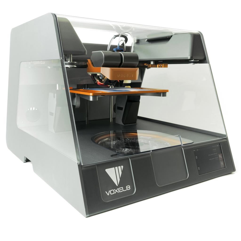
33 3D Printing Circuits Voxel8 32
34 Logistics 33 Find Partners 2 for labs up to 3 for projects Lab2 section tomorrow 4-5p Jacobs 220 no section this Monday Lab2 gear Borrow nucleos: buy later, bring more tomorrow Need breadboards and wires + microusb cable Sign up for Othermill training three slots between now and next Thursday Alternative slots: Fri 2-3:30p, Tue 5:30-7p, Wed 1-2:30p
35 Next Time 34 Milling boards Assembly and soldering
36 References 35 Learn Eagle: https: //learn.sparkfun.com/tutorials/using-eagle-board-schematic and https: //learn.sparkfun.com/tutorials/using-eagle-board-layout Printed Circuit Boards on Wikipedia: RobotRoom Articles: AlternateZone PCB Tutorial: electronics/files/pcbdesigntutorialreva.pdf EE4: Circuit Board Design by Ducky Lin for CalSol team
courtesy Wikipedia user Wikinaut
 What's a PCB? https://learn.sparkfun.com/tutorials/pcb-basics Printed circuit board is the most common name but may also be called printed wiring boards or printed wiring cards. Before the advent of the
Generic Multilayer Specifications for Rigid PCB s
 Generic Multilayer Specifications for Rigid PCB s 1.1 GENERAL 1.1.1 This specification has been developed for the fabrication of rigid SMT and Mixed Technology Multilayer Printed Circuit Boards (PCB's)
PCB Production Methods
 PCB Production Methods PCB Development Process Summary Manufacturing Constraints Gerber Schematic Board Manufacture This is art! Ensure that the schematic is accurate. Run the ERC often. This is art! Ensure
Milling PCBs. Jonathan Bachrach. September 14, EECS UC Berkeley
 Milling PCBs Jonathan Bachrach EECS UC Berkeley September 14, 2016 Last Time 1 PCBs wisegeek Today 2 Milling PCBs CNC 3 Computerized Numeric Control Benefits 4 Automation Precision Repeatability Flexibility
Sectional Design Standard for Flexible/Rigid-Flexible Printed Boards
 Sectional Design Standard for Flexible/Rigid-Flexible Printed Boards Developed by the Flexible Circuits Design Subcommittee (D-) of the Flexible Circuits Committee (D-0) of IPC Supersedes: IPC-2223C -
Creating another Printed Circuit Board
 Appendix C Creating another Printed Circuit Board In this chapter, we will learn the following to World Class standards: Starting with a Finished Schematic Creating the Layers for the Printed Circuit Board
Processing Gerber Files in CircuitPro
 Processing Gerber Files in CircuitPro Requirements 1. Circuit Pro version 1.5 revision 164 or higher 2. Set of Gerber Files Process Steps 1. Execute Process Planning Wizard. a. Press the process planning
Allegro New Products - DFM / Rule Checkers
 Allegro New Products - DFM / Rule Checkers Eric / Graser 16 / Oct / 2015 Topic Allegro DFM Checker in Allegro PCB Manufacturing Option Allegro PCB Rules Developer / Checker Option PCB Design & Production
Sunstone Circuits DFMplus Summary Report
 Job Name DFM081-wireless_controller_v0 Part Number Wireless_Controller Customer Name Contact Name Job Class IPC Class 2 Job View Creation Time 2014-08-14 15:55:31 Revision V0 Operator Name lyndap Contact
DESIGN FOR MANUFACTURABILITY (DFM)
") T H A N K S F O R A T T E N D I N G OUR TECHNICAL WEBINAR SERIES DESIGN FOR MANUFACTURABILITY (DFM) Presented by: We don t just sell PCBs. We sell sleep. Cirtech EDA is the exclusive SA representative
T H A N K S F O R A T T E N D I N G OUR TECHNICAL WEBINAR SERIES DESIGN FOR MANUFACTURABILITY (DFM) Presented by: We don t just sell PCBs. We sell sleep. Cirtech EDA is the exclusive SA representative
ECE453 Lab 5: FM Quadrature Demodulation / PCB Design Using Eagle
 ECE453 Lab 5: FM Quadrature Demodulation / PCB Design Using Eagle In this lab, you will work with your partner to design a printed circuit board for a quadrature demodulator IC and supporting components.
PCB layout tutorial MultiSim/Ultiboard
 PCB layout tutorial MultiSim/Ultiboard The basic steps in designing a PCB Paper design and prototype of the basic circuit. Identify the parts and the footprints that will be used. Make a circuit schematic,
Value Stream Map Process Flow
 Value Stream Map Process Flow Pre- Locate Data Value Stream Mapping Has The Following Characteristics: It Is A Comprehensive And Detailed Graphical Document That Lists Every Business Unit, Organization,
Page 1
 CONTENT INTRODUCTION 2 INPUT DATA FORMATS 3 INPUT DATA REQUIREMENTS 4 CLASSIFICATION 6 HOLES 8 COPPER LAYERS 10 BGAS 12 MECHANICAL LAYER 13 SOLDERMASK 15 LEGEND PRINT 17 CARBON 18 PEEL-OFF MASK 19 VIAFILL
Plated Through Hole Components. Padstack. Curso Prof. Andrés Roldán Aranda. 4º Curso Grado en Ingeniería de Tecnologías de Telecomunicación
 Plated Through Hole Components Padstack Curso 15-16 Prof. Andrés Roldán Aranda 4º Curso Grado en Ingeniería de Tecnologías de Telecomunicación 1.- Arquitectura del Pad 2.- Conceptos 3.- Tipología de Pads
RF circuit fabrication rules
 RF circuit fabrication rules Content: Single layer (ref. page 4) No vias (ref. page 4) With riveted vias (ref. pages 4,5,6) With plated vias (ref. pages 4, 5,7,8,9,10,11) Component assembly (ref. pages
Printed circuit boards-solder mask design basics
 Printed circuit boards-solder mask design basics Standards Information on the use of solder mask is contained in IPC-SM-840C Qualification and Performance of Permanent Solder Mask. The specification is
Design For Manufacture
 NCAB Group Seminar no. 11 Design For Manufacture NCAB GROUP Design For Manufacture Design for manufacture (DFM) What areas does DFM give consideration to? Common errors in the documentation Good design
South Bay Circuits. Manufacturability Guidelines. Printed Circuit Boards FOR. South Bay Circuits, Inc. 99 N. McKemy Ave Chandler, AZ 85226
 Manufacturability Guidelines FOR Printed Circuit Boards South Bay Circuits, Inc. 99 N. McKemy Ave Chandler, AZ 85226 GL-0503B By: Edward Rocha Dear Customer, The intention of this document is to provide
PCB Fundamentals Quiz
 1. PCBs should be fabricated with layers. a. Odd Number of b. Even Number of c. Any Number of 2. Which of the following is not taken into consideration when calculating the characteristic impedance for
Introduction to NI Multisim & Ultiboard Software version 14.1
 School of Engineering and Applied Science Electrical and Computer Engineering Department Introduction to NI Multisim & Ultiboard Software version 14.1 Dr. Amir Aslani August 2018 Parts Probes Tools Outline
Application Bulletin 240
 Application Bulletin 240 Design Consideration CUSTOM CAPABILITIES Standard PC board fabrication flexibility allows for various component orientations, mounting features, and interconnect schemes. The starting
CAPABILITIES Specifications Vary By Manufacturing Locations
 Revised June 2011 Toll Free: 1-800-979-4PCB (4722) www.4pcb.com sales@4pcb.com Material FR4 RoHS RF Materials CAPABILITIES Specifications Vary By Manufacturing Locations Number of Conductive Layers Standard
IEEE #: March 24, Rev. A
 Texas Tech University Electrical Engineering Department IEEE Student Branch Milling Tutorial An EE s Guide to Using the Milling Machine Written by: Juan Jose Chong Photos by: David Hawronsky IEEE #: 90499216
Tutorial In Practical Circuit Board Design Ben LeVesque ECE480 Team 3 November 9 th, 2007
 utorial In Practical Circuit Board Design Ben LeVesque ECE480 eam 3 November 9 th, 2007 Keywords Circuit board, Cadence, Layout, Capture, post processing, trace capacity, trace ampacity, Via Abstract his
Technology Flexible Printed Circuits Rev For latest information please visit
 Options and Characteristics Online calculation On explicit enquiry Quantity 1 pieces up to 1m² total area 1piece to mass production Number of layers 1 to 2 layers up to 6 layers Material thickness 0,05mm
Artwork: (A/W) An accurately scaled configuration used to produce the artwork master or production master.
 An accurately scaled configuration used to produce the artwork master or production master.") Adhesive: The material used for bonding two substrates of material together. (usually; LF of FR 0100) Adhesive Squeeze-Out: Adhesive will ooze out slightly during the lamination cycle. Annular Ring: That
Adhesive: The material used for bonding two substrates of material together. (usually; LF of FR 0100) Adhesive Squeeze-Out: Adhesive will ooze out slightly during the lamination cycle. Annular Ring: That
EECAD s MUST List. Requests for drawing numbers MUST be submitted via the EECAD job request form at
 Customers are required to follow certain criteria for all designs whether they are ultimately done in EECAD or by the customers themselves. These criteria, approved by EES Management, are listed below:
Wiring Projects. Chapter 5 Wiring Diagrams March 29, Wire List Wire List 3/28/2010
 Chapter 5 Wiring Diagrams March 29, 2010 Wiring Projects Electronic schematics are required to completely describe how the wiring will be connected to the components. The Cad Technician will develop the
Printed Electronic Design
 Published on Online Documentation for Altium Products (https://www.altium.com/documentation) Home > Printed Electronics Using Altium Documentation Modified by Phil Loughhead on Dec 11, 2018 Printed Electronic
Processing parameters of PCBs manufactured by TS PCB Techno-Service S.A.
 Processing parameters of PCBs manufactured by TS PCB Techno-Service S.A. Last update: jh 26.09.2017 Table of contents 1. Processing parameters of PCB materials... 3 1.1. Applied laminate types... 3 1.2.
PCB Fundamentals Quiz
 1. PCBs should be fabricated with layers. a. Odd Number of b. Even Number of c. Any Number of Reason: Using an odd number of layers may result in board warpage. 2. Which of the following is not taken into
Wire Epoxy filled groove
 147 Appendix D Finger construction steps In this procedure, \Upper mask" refers to a piece of copper which has been photomasked with the resist pattern for the upper electrodes and \lower mask" refers
Design for Manufacturing
 2 Design for Manufacturing This chapter will address the fabrication process of the PCB and the requirements of the manufacturer. Manufacturers are separated by their limitations or constraints into categories
Michael R. Creeden CEO/CID+ San Diego PCB, Inc. & EPTAC (858)
") Michael R. Creeden CEO/CID+ San Diego PCB, Inc. & EPTAC mike.creeden@sdpcb.com (858)271-5722 1. Why we collaborate? 2. When do we collaborate? 3. Who do we collaborate with? 4. What do we collaborate?
Michael R. Creeden CEO/CID+ San Diego PCB, Inc. & EPTAC mike.creeden@sdpcb.com (858)271-5722 1. Why we collaborate? 2. When do we collaborate? 3. Who do we collaborate with? 4. What do we collaborate?
PCB Artist Quickstart Guide Revision 01
 UT DALLAS Erik Jonsson School of Engineering & Computer Science PCB Artist Quickstart Guide Revision 01 Pete Semig Ph.D. Student-Dr. Jafari Analog Application Engineer-TI 1 Important Terminology PCB Artist
Test Pattern Artwork and Sample
 www.nts.com 1.800.270.2516 Test Pattern Artwork and Sample Preparation for UL 796 This document is intended to assist NTS' customers with preparing their samples for submission for testing under the Client
What the Designer needs to know
 White Paper on soldering QFN packages to electronic assemblies. Brian J. Leach VP of Sales and Marketing AccuSpec Electronics, LLC Defect free QFN Assembly What the Designer needs to know QFN Description:
ELECTRICAL CONNECTIONS
 ELECTRICAL CONNECTIONS Lesson 13 EET 150 Electrical Connections Learning Objectives In this lesson you will: see different methods of making electrical connections. learn a procedure for making soldered
Getting Started in Eagle Professional Schematic Software. Tyler Borysiak Team 9 Manager
 Getting Started in Eagle 7.3.0 Professional Schematic Software Tyler Borysiak Team 9 Manager 1 Executive Summary PCBs, or Printed Circuit Boards, are all around us. Almost every single piece of electrical
Optimalisation of the PCB design and PCB production to control cost
 Optimalisation of the PCB design and PCB production to control cost Edward Snelleman 1 Introduction Q.P.I. Group 1988 started to be active in the field of PCB supply/development and PCB Design 2015 member
Design For Manufacturability
 Colonial ELECTRONIC MANUFACTURERS, INCORPORATED Design For Manufacturability GUIDELINES DFM-1 REV-C One Chestnut Street Nashua, New Hampshire 03060 Telephone: (603) 881-8244 FAX: (603) 881-8186 1 DFM-1
TD-DEV V Technical Specification
 High-Efficiency MODULE Carrier Board TD-DEV-500-12V Technical Specification POWER SUPPLY TECHNOLOGY FEATURES Low profile 1U, 500W power supply High efficiency power supply Fully integrated with CPU control
Innovative pcb solutions used in medical and other devices Made in Switzerland
 Innovative pcb solutions used in medical and other devices Made in Switzerland Chocolate Watches Money.PCB`s innovative pcb`s... Customer = innovation driver Need to add more parts and I/O make smaller/thinner
Altium I (Circuit Design + Layout)
") Altium I (Circuit Design + Layout) ELEC391 Summer T1 2018 Contents PCB Design support for ELEC391 PCB design flow How to install Altium Designer 2016 Understanding Altium Designer Walk-through example
Altium I (Circuit Design + Layout) ELEC391 Summer T1 2018 Contents PCB Design support for ELEC391 PCB design flow How to install Altium Designer 2016 Understanding Altium Designer Walk-through example
Z-Wrap-110 Loss 31 July 01
 Z-Wrap-11 Loss 31 July 1 Z-Axis J. Sortor TEST METHOD: To accurately measure complex impedance, it is required that the network analyzer be calibrated up to the phase plane of the unit under test (UUT).
Low-Cost PCB Design 1
 Low-Cost PCB Design 1 PCB design parameters Defining PCB design parameters begins with understanding: End product features, uses, environment, and lifetime goals PCB performance, manufacturing, and yield
ATTRIBUTES STANDARD ADVANCED
 TECHNOLOGY MATRIX 2017 ATTRIBUTES STANDARD ADVANCED Line/Space.005 /.005.003 /.003 Copper Foil. Oz. Min/Max ½ / 2 3 / 8 Pad Size Int. (dia over Drill).014.008 Pad Size Ext. (dia over Drill).012.008 Drill-to-Metal
Our Top 10 Commonly Asked Soldering Questions This Year
 Our Top 10 Commonly Asked Soldering Questions This Year 1 Chip Component Shifting Can be related to components floating on the molten solder plus the equipment may have vibrations, which may not be felt
Wheatstone Bridge. M16C Microcontroller Strain Gauge (temperature compensation)
") Overview Eagle Version: 5.11.0 Circuit: Strain gauge amplifier for interface with a microcontroller. Time Requirements 2 + 2 + 2 hours. This three part guide is intended to provide an introduction to PCB
Overview Eagle Version: 5.11.0 Circuit: Strain gauge amplifier for interface with a microcontroller. Time Requirements 2 + 2 + 2 hours. This three part guide is intended to provide an introduction to PCB
EECO-Green SILVER-THROUGH-HOLE DOUBLE-SIDED PRINTED CIRCUIT BOARDS
 EECO-Green SILVER-THROUGH-HOLE DOUBLE-SIDED PRINTED CIRCUIT BOARDS PRODUCT OVERVIEW DESIGN CONSIDERATIONS FAQ s 880 Columbia St. Brea, CA 92821 TEL: (714) 835-6000 FAX: (714) 482-9429 Web: www.eecoswitch.com
PCB Design (with EAGLE tutorial) TA: Robert Likamwa ELEC 424, Fall 2010
 TA: Robert Likamwa ELEC 424, Fall 2010") PCB Design (with EAGLE tutorial) TA: Robert Likamwa ELEC 424, Fall 2010 Printed Circuit Boards What are they? How can I make one? 424 Project description Eagle Tutorial http://www.electronicmanufacturers.co.za/
PCB Design (with EAGLE tutorial) TA: Robert Likamwa ELEC 424, Fall 2010 Printed Circuit Boards What are they? How can I make one? 424 Project description Eagle Tutorial http://www.electronicmanufacturers.co.za/
2x2 mm LGA Package Guidelines for Printed Circuit Board Design. Figure 1. 2x2 mm LGA package marking information.
 2x2 mm LGA Package Guidelines for Printed Circuit Board Design This technical note is intended to provide information about Kionix s 2 x 2 mm LGA packages and guidelines for developing PCB land pattern
The Swiss Army Knife for the Lab Micro Material Processing with the LPKF ProtoLaser U4
 The Swiss Army Knife for the Lab Micro Material Processing with the LPKF ProtoLaser U4 Micro Machining in the Lab LPKF ProtoLasers have been in use in leading electronics laboratories around the world
Published on Online Documentation for Altium Products (http://www.altium.com/documentation)
") Published on Online Documentation for Altium Products (http://www.altium.com/documentation) Главная > Controlled Depth Drilling, or Back Drilling Новая эра документации Modified by Jun Chu on Apr 11, 2017
Published on Online Documentation for Altium Products (http://www.altium.com/documentation) Главная > Controlled Depth Drilling, or Back Drilling Новая эра документации Modified by Jun Chu on Apr 11, 2017
TCLAD: TOOLS FOR AN OPTIMAL DESIGN
 TCLAD: TOOLS FOR AN OPTIMAL DESIGN THINGS TO CONSIDER WHEN DESIGNING CIRCUITS Many factors come into play in circuit design with respect to etching, surface finishing and mechanical fabrication processes;
AltiumLive 2017: Creating Documentation for Successful PCB Manufacturing
 AltiumLive 2017: Creating Documentation for Successful PCB Manufacturing Julie Ellis TTM Field Applications Engineer Thomas Schneider Field Applications Engineer 1 Agenda 1 Complexity & Cost 2 3 4 5 6
First-aid kits for circuit boards, time-tested and guaranteed.
 First-aid kits for circuit boards, time-tested and guaranteed. CircuitMedic kits have been specifically designed to meet the requirements outlined in repair and rework guidelines published by IPC, the
PCB Layout. Date : 22 Dec 05. Prepare by : HK Sim Prepare by : HK Sim
 PCB Layout Date : 22 Dec 05 Main steps from Schematic to PCB Move from schematic to PCB Define PCB size Bring component from schematic to PCB Move the components to the desire position Layout the path
NextGIn( Connec&on'to'the'Next'Level' Application note // DRAFT Fan-out 0,50mm stapitch BGA using VeCS. Joan Tourné NextGIn Technology BV
 NextGIn( Connec&on'to'the'Next'Level' Application note // DRAFT Fan-out 0,50mm stapitch BGA using VeCS. Joan Tourné NextGIn Technology BV February 27 th 2017 In this document we describe the use of VeCS
First-Aid Kits for Circuit Boards
 First-Aid Kits for Circuit Boards CircuitMedic kits have been specifically designed to meet the requirements outlined in repair and rework guidelines published by IPC, the leading electronics manufacturing
TECHNICAL REPORT: CVEL Parasitic Inductance Cancellation for Filtering to Chassis Ground Using Surface Mount Capacitors
 TECHNICAL REPORT: CVEL-14-059 Parasitic Inductance Cancellation for Filtering to Chassis Ground Using Surface Mount Capacitors Andrew J. McDowell and Dr. Todd H. Hubing Clemson University April 30, 2014
Gerber Setup. Summary. Access. Options/Controls. General Tab. Modified by on 13-Sep Parent page: WorkspaceManager Dialogs
 Gerber Setup Old Content - visit altium.com/documentation Modified by on 13-Sep-2017 Parent page: WorkspaceManager Dialogs Summary Each Gerber file corresponds to one layer in the physical board the component
Printed Circuit Techniques
 Experiment # 0 Printed Circuit Techniques INTRODUCTION: More than 40 years after they first appeared, the printed-circuit boards (PCBs) are still the most important means of connecting components into
14.8 Designing Boards For BGAs
 exposure. Maintaining proper control of moisture uptake in components is critical to the prevention of "popcorning" of the package body or encapsulation material. BGA components, before shipping, are baked
Using EAGLE: Board Layout a
 Using EAGLE: Board Layout a learn.sparkfun.com tutorial Available online at: http://sfe.io/t111 Contents Previously on Using EAGLE Layers Overview Arranging the Board Routing the Board Checking for Errors
Inspection Method Sheet
 Inspection Method Sheet Part Number: Generic Part Name: PCB Filters Drawing Number: Generic Operation: In Process / Final Page 1 of 10 Written By: Myra Cope Doc. #: TT-PC-0378 Rev. 14 Date: 10-15-08 Applicable
WIRE LAYING METHODS AS AN ALTERNATIVE TO MULTILAYER PCB Sf
 Electrocomponent Science and Technology, 1984, Vol. 11, pp. 117-122 (C) 1984 Gordon and Breach Science Publishers, Inc 0305-3091/84/1102-0117 $18.50/0 Printed in Great Britain WIRE LAYING METHODS AS AN
Technology Overview. Blind Micro-vias. Embedded Resistors. Chip-on-flex. Multi-Tier Boards. RF Product. Multi-chip Modules. Embedded Capacitance
 Blind Micro-vias Embedded Resistors Multi-Tier Boards Chip-on-flex RF Product Multi-chip Modules Embedded Capacitance Technology Overview Fine-line Technology Agenda Corporate Overview Company Profile
METRIC PITCH BGA AND MICRO BGA ROUTING SOLUTIONS
 White Paper METRIC PITCH BGA AND MICRO BGA ROUTING SOLUTIONS June 2010 ABSTRACT The following paper provides Via Fanout and Trace Routing solutions for various metric pitch Ball Grid Array Packages. Note:
CAPABILITIES OF SYNERGISE PCB INC
 CAPABILITIES OF SYNERGISE PCB INC 2 Surface Treatment Surface Treatment Selective Surface Treatment HASL, L/F HASL, ENIG, Immersion Silver, Hard Gold(Plated gold), Flash Gold, Immersion Tin/Silver, OSP
MSL RAD Front-End-Electronics RADE PCB layout
 MSL RAD Front-End-Electronics RADE PCB layout Stephan I. Böttcher v04: December 12, 2006 The RADE board supports the readout of the neutron channel scintillator of the RAD instrument. The board will be
An Introduction to Electronics Systems Packaging. Prof. G. V. Mahesh. Department of Electronic Systems Engineering
 An Introduction to Electronics Systems Packaging Prof. G. V. Mahesh Department of Electronic Systems Engineering Indian Institute of Science, Bangalore Module No. # 07 Lecture No. # 33 Reflow and Wave
PCB technologies and manufacturing General Presentation
 PCB technologies and manufacturing General Presentation 1 Date : December 2014 3 plants for a global offer dedicated to the European market and export Special technologies, Harsh environment PCB for space
TN008. PCB Design Guidelines for 2x2 LGA Sensors. Introduction. 2x2 LGA Package Marking
 PCB Design Guidelines for 2x2 LGA Sensors Introduction This technical note is intended to provide information about Kionix s 2 x 2 mm LGA packages and guidelines for developing PCB land pattern layouts.
PCB Design considerations
 PCB Design considerations Better product Easier to produce Reducing cost Overall quality improvement PCB design considerations PCB Design to assure optimal assembly Place at least 3 fiducials (global fiducial)
Sectional Design Standard for High Density Interconnect (HDI) Printed Boards
 Printed Boards") IPC-2226 ASSOCIATION CONNECTING ELECTRONICS INDUSTRIES Sectional Design Standard for High Density Interconnect (HDI) Printed Boards Developed by the HDI Design Subcommittee (D-41) of the HDI Committee
IPC-2226 ASSOCIATION CONNECTING ELECTRONICS INDUSTRIES Sectional Design Standard for High Density Interconnect (HDI) Printed Boards Developed by the HDI Design Subcommittee (D-41) of the HDI Committee
CAD Layout Recommendations for the PowerBlox Family
 Solved by APPLICATION NOTE ANP4 TM CAD Layout Recommendations for the PowerBlox Family Introduction The Sipex PowerBlox family of parts offers designers a very high power density solution for wide input
Release your hardware hacker potential with KiCAD. Eric Thompson LowVoltageLabs.com
 Release your hardware hacker potential with KiCAD Eric Thompson LowVoltageLabs.com Create a board with KiCAD What is a PCB? What is a KiCAD? Block diagram Schematic Schematic attribute editor Error check
Line-Following Robot
 1 Line-Following Robot Printed Circuit Board Assembly Jeffrey La Favre October 5, 2014 After you have learned to solder, you are ready to start the assembly of your robot. The assembly will be divided
Pacific Antenna RF Probe assembly
 Pacific Antenna RF Probe assembly Parts In the Kit: 1 1/2 x 3 Blue PEX tube 2 5/8 O.D. vinyl caps 2 3/32 dia x 2 brass tube sections 2 Pogo spring contacts 1 4-40 x 7/16 pan head screw 1 4-40 x 1/4 pan
Design Guide for High-Speed Controlled Impedance Circuit Boards
 IPC-2141A ASSOCIATION CONNECTING ELECTRONICS INDUSTRIES Design Guide for High-Speed Controlled Impedance Circuit Boards Developed by the IPC Controlled Impedance Task Group (D-21c) of the High Speed/High
Gerber Setup. Modified by Susan Riege on 4-Aug Parent page: WorkspaceManager Dialogs
 Gerber Setup Modified by Susan Riege on 4-Aug-2015 Parent page: WorkspaceManager Dialogs Other Related Resources Options for Project - Options Tab (Dialog) Generate Output Files (Dialog) Aperture (Dialog)
LPKF TechGuide In-House PCB Prototyping
 LPKF TechGuide In-House PCB Prototyping Do you have any Questions about your Order? Do you Require Technical Support? You can find all sales and service contact information below. Our experienced employees
Product Specification - LPM Connector Family
 LPM Product Specification - LPM OVERVIEW Developed for mobile devices and other space-constrained applications, the Neoconix LPM line of connectors feature exceptional X-Y-Z density with a simple, highly
PCB Manufacture Capabilities
 Item Unit Description or parameter 1 Arlon material model AD350,AR1000,25FR,33N,Diclad527 2 Rogers material model Ro4350,Ro4350B,Ro4003,Ro4003C,Ro3003,RT5880 3 Rogers PP model Ro4403(0.10mm),Ro4450B(0.10mm),
Controlled Impedance Test
 Controlled Impedance Test by MARTYN GAUDION The increasing requirement for controlled impedance PCBs is well documented. As more designs require fast data rates, and shrinking dies on new silicon mean
Overcoming the Challenges of HDI Design
 ALTIUMLIVE 2018: Overcoming the Challenges of HDI Design Susy Webb Design Science Sr PCB Designer San Diego Oct, 2018 1 Challenges HDI Challenges Building the uvia structures The cost of HDI (types) boards
IT STARTS WITH THE DESIGN: THE CHALLENGE: THE PROBLEM: Page 1
 High Performance Multilayer PCBs Design and Manufacturability Judy Warner, Transline Technology Chris Savalia, Transline Technology Michael Ingham, Spectrum Integrity IT STARTS WITH THE DESIGN: Multilayer
Quiz Design Question. Signal Grounds. Wires Theory vs Reality
 Quiz Design Question Quiz Thu 2:30p The design question will involve one of Op amp or BJT(s) or MOSFET(s). One or more of these datasheets will be included in the exam: OP AMP http://web.mit.edu/6.101/www/reference/lm741.pdf
How to solder SMD component on Awesome PCB or any other kind of PCB.
 How to solder SMD component on Awesome PCB or any other kind of PCB. Step by step tutorial, with no steps to skip. Step 1 - What do we need? Step 2 - Fixing PCB Step 3 - Preparing for soldering Step 4
FPC connectors (0.3mm pitch) Front lock with FPC tabs
 Front lock with FPC tabs") AYF31 For FPC FPC connectors (0.3mm pitch) Front lock with FPC tabs Y3FT Series FEATURES 1. Low-profile, space-saving design (pitch: 0.3mm) The 0.9mm height, 3.0mm depth contributes to the miniaturization
AYF31 For FPC FPC connectors (0.3mm pitch) Front lock with FPC tabs Y3FT Series FEATURES 1. Low-profile, space-saving design (pitch: 0.3mm) The 0.9mm height, 3.0mm depth contributes to the miniaturization
RD51 ANNUAL REPORT WG1 - Technological Aspects and Development of New Detector Structures
 RD51 ANNUAL REPORT 2009 WG1 - Technological Aspects and Development of New Detector Structures Conveners: Serge Duarte Pinto (CERN), Paul Colas (CEA Saclay) Common projects Most activities in WG1 are meetings,
For FPC. FPC connectors (0.2mm pitch) Back lock
 Back lock") 0.9 For FPC FPC connectors (0.2mm pitch) Back lock Y2B Series AYF21 New FEATURES 1. Slim and low profile design (Pitch: 0.2 mm) 0.2 mm pitch back lock design and the slim body with a 3.15 mm depth (with
0.9 For FPC FPC connectors (0.2mm pitch) Back lock Y2B Series AYF21 New FEATURES 1. Slim and low profile design (Pitch: 0.2 mm) 0.2 mm pitch back lock design and the slim body with a 3.15 mm depth (with
Design Analysis Process
 Prototype Design Analysis Process Rapid Prototyping What is rapid prototyping? A process that generates physical objects directly from geometric data without traditional tools Rapid Prototyping What is
High currents in safe paths
 High currents in safe paths Webinar November 3 rd 2015 Speaker: Andreas Schilpp www.we-online.de topics Flex-rigid technology with thick copper layers Update Design Rules Wirelaid Update UL-Listing Wirelaid
Rapid Prototyping Introduction ENGR 1182
 Rapid Prototyping Introduction ENGR 1182 Objectives What is Rapid Prototyping? How a 3D printer works 3D Printing in EED Laser Cutting in EED Design your own part option What is Rapid Prototyping? Rapid
For FPC. FPC connectors (0.3mm pitch) Back lock
 Back lock") 0.9 For FPC FPC connectors (0.3mm pitch) Back lock AYF33 Y3B/Y3BW Series New Y3B Y3BW is added. FEATURES 1. Slim and low profile design (Pitch: 0.3 mm) Back lock type and the slim body with a 3.15 mm depth
0.9 For FPC FPC connectors (0.3mm pitch) Back lock AYF33 Y3B/Y3BW Series New Y3B Y3BW is added. FEATURES 1. Slim and low profile design (Pitch: 0.3 mm) Back lock type and the slim body with a 3.15 mm depth
EMI Shielding and Grounding Materials
 EMI Shielding and Grounding Materials P-SHIELD Shielding and Grounding Materials Polymer Science, Inc. offers a complete EMI shielding and grounding materials product line. P-SHIELD EMI shielding materials
PCB Supplier of the Best Quality, Lowest Price and Reliable Lead Time. Low Cost Prototype Standard Prototype & Production Stencil PCB Design
 The Best Quality PCB Supplier PCB Supplier of the Best Quality, Lowest Price Low Cost Prototype Standard Prototype & Production Stencil PCB Design Visit us: www. qualiecocircuits.co.nz OVERVIEW A thin