Page 1
|
|
|
- Patricia Glenn
- 5 years ago
- Views:
Transcription
1 CONTENT INTRODUCTION 2 INPUT DATA FORMATS 3 INPUT DATA REQUIREMENTS 4 CLASSIFICATION 6 HOLES 8 COPPER LAYERS 10 BGAS 12 MECHANICAL LAYER 13 SOLDERMASK 15 LEGEND PRINT 17 CARBON 18 PEEL-OFF MASK 19 VIAFILL 20 HEATSINK PASTE 21 TRACK WIDTH GRAPHIC 22 Page 1
2 Introduction These Guidelines set out best practice to reduce the cost of your boards and to minimize the risk of errors arising during manufacture. Not all possible PCB design features are available on all our services. Look at our services overview to see more details. On some specific features we highlight the availability in a particular service. The world is divided into a part that works with the Metric system and a part that works with the Imperial system for defining measurements. The µm is 25.4 times smaller than the Mil. Dimensions for electronics are driven smaller all the time. To ensure the highest quality possible, we decided many years ago to work exclusively in the Metric system in our front end department. Therefore the basis of all measurements given in this document and in our website is the Metric system. All Imperial values are there for clarification and general understanding only. There is no general consensus throughout the global PCB industry on terminology, so if we feel any term we use may be unclear we have tried to explain it when it first appears. Page 2
3 Input data formats Accepted data formats for PCB layout data are: Artwork: - Gerber RS-274X (Extended Gerber with embedded apertures - developed by Gerber Systems) - DPF (Dynamic Process Format - developed by Ucamco NV) - Gerber RS-274D (Standard Gerber with a separate aperture file - developed by Gerber Systems) - Eagle.BRD file (CAD-data from CADsoft now Farnell) Artwork means all copper layers, soldermask and legend layers, board outline or mechanical layer, SMD paste layers, carbon layers, peel-off layers, etc. Drilling: - Excellon (1 or 2) + appropriate tool list (ideally embedded) - Sieb&Meyer + appropriate tool list (ideally embedded) - Gerber format RS-274X or RS-274D (only true drill data, not a drill map) - DPF (only true drill data, not a drill map) Please supply ONLY ASCII-encoded files. These files are man-readable so that our engineers can check them visually if needed during data preparation. So we don t accept formats such as EIA or EBCDIC. CAD PCB design data, other than from EAGLE, is NOT ACCEPTED! We do not accept CAD PCB design data other than EAGLE. 1. Converting CAD data into production data may lead to errors which we cannot cross-check 2. It is impossible to have legal copies of every CAD PCB design package in the market and to have the necessary knowledge to use them all correctly. As designers do not all use the same software version, we would need to have a whole range of update patches as well. Gerber is clear and unambiguous. It has been the industry-standard format for PCB manufacture for many years. Every PCB design package can output Gerber data and the process will be fully described in your CAD PCB design package handbook or help-files. You can check the accuracy of the Gerber output data by downloading one of the many free Gerber viewers available on the internet. We recommend GC-Prevue available as freeware from Page 3
 - For Drilling -- Excellon1 + appropriate tool list (ideally embedded) PCB Visualizer: For reasons of automated analysis and")

 from the single board data to your individual specification, the panel plan can be supplied as a Gerber or DPF file.")
 either using PCB Visualizer or with a Gerber viewer before you send it on to production.")
4 Input data requirements 1. Preferred data formats are: - For Artwork -- Extended Gerber (RS-274X) - For Drilling -- Excellon1 + appropriate tool list (ideally embedded) PCB Visualizer: For reasons of automated analysis and visualisation, the PCB Visualizer only accepts Extended Gerbers (RS-274X) or an EAGLE.BRD file. 2. Provide us ONLY with the data files needed for production. These are: - Gerber files for the copper layers, soldermask and legend layers, mechanical layer and SMD paste layers. Plus carbon, peel-off and via-fill layers as needed. - Excellon drill file(s) for drilling. - If you want us to prepare a customer panel ( array, matrix or biscuit ) from the single board data to your individual specification, the panel plan can be supplied as a Gerber or DPF file. Please DO NOT provide any additional files such as original CAD data (other than Eagle), Graphicode GWK files, PDF files, Word files (doc), Excel files (xls), part lists, placement and assembly information, etc. Where possible check your generated output data (Gerber & Excellon files) either using PCB Visualizer or with a Gerber viewer before you send it on to production. Make sure that all instructions or other necessary input needed for making the boards are included in the Gerber and Excellon files. 3. Use clear and easy to understand file naming and try to avoid long filenames. Make sure that we can easy determine the layer function from the filename. Good file naming: File naming is too long, not advisable: Bad file naming: no info on layer function in the file names: 4. DO NOT scale your data. All data provided must be scale 1/1 (100%). 5. Make sure that your Gerber files DO NOT contain apertures with a zero-size (size = 0.00mm or inches) and that your Excellon data DOES NOT have zero-sized tools (size=0.00mm or inches). Page 4
 in your Gerber & Excellon output files as in your CAD PCB design software.")
 used for your output (Gerber & Excellon) is at least a factor 10 better than the resolution (grid) used in your CAD PCB design")


5 6. Use the same offset for all your Gerber layers and the Excellon drill data. Preferably use no offset at all. All layers have a different offset! All layers have the same offset 7. Use the same units (mm or inch) in your Gerber & Excellon output files as in your CAD PCB design software. This will eliminate conversion or rounding errors. 8. Use the same resolution (grid) for your Gerber & Excellon data to allow a perfect match. Also make sure that the resolution (grid) used for your output (Gerber & Excellon) is at least a factor 10 better than the resolution (grid) used in your CAD PCB design software. Example: If you use a 10 mil resolution to draw your board in your CAD PCB design software, then use a 1mil output resolution for your Gerber & Excellon output. 9. Make sure that your data is supplied as seen from top to bottom through the PCB. DO NOT mirror (or reflect) any data layer image or drill. Viewing a PCB from top to bottom through the board is the universal practice in the PCB industry. We view and handle your data in that way, as does your CAD PCB design software. -> This means that when viewing your Gerber data, text on the top side of your board (copper, soldermask, legend) should be readable and text on the bottom side (copper, soldermask, legend) should be non-readable (= mirrored). Page 5

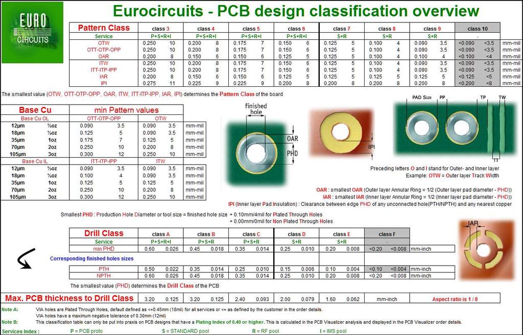
6 10. Put some small text (board identification, company name, etc...) in the copper layers. Make sure the text complies with the readability rules. This will help us to avoid mirroring errors. 11. RECOMMENDATION. In your Gerber files use flashed pads as often as possible. 12. RECOMMENDATION. In your CAD PCB design software try to create an aperture list for Gerber output which only shows the apertures used in the design. 13. Make sure that you include the board outline on all layers. This will enable us to properly align all layers in case of an offset problem. Also include the board outline in a separate Gerber mechanical plan. Classification Introduction We use pattern classes and drill classes as convenient shorthand to measure the manufacturability of the PCB. This controls whether the board can be pooled or not and has an impact on the pricing. The pattern class covers The minimum sizes for copper track (conductor) and gap (isolation) for Outer and Inner layers: - Outer layers OTT = Track to Track, OTP = Track to Pad, OPP = Pad to Pad and OTW = Track Width - Inner layers ITT = Track to Track, ITP = Track to Pad, IPP = Pad to Pad and ITW = Track Width The minimum copper rings on outer and inner layers (OAR = Outer Annular Ring, IAR = Inner Annular Ring) The minimum IPI (Inner layer Pad Isolation): IPI is the clearance between the edge of any unconnected hole (plated or non-plated) and the nearest copper (plane, track, pad). This is measured from the production tool size. Minimum IPI value is always IAR +75µm (3mil) The smallest of these values determines the pattern class. The drill class is based on the smallest production tool size on the board. For more information see the current Classification table on the next page Annular Ring calculations are done from the production TOOLSIZE for the holes, not from the finished hole ENDSIZE. --> For the conversion rules for ENDSIZE to TOOLSIZE see Holes section The Classification table shows the lower limit values of any given class. 2. The Annular Ring values OAR and IAR in the classification table are for plated holes (PTH). For connected non-plated (NPTH) holes we recommend a minimum annular ring of 0.30mm (12mil). As NPTH holes have no plated barrel, a smaller annular ring may lift during soldering or break away even during normal operating conditions. 3. The thickness of the starting copper foil determines the minimum pattern values that are possible. This means that the highest pattern class possible depends on the copper thicknesses. Thicker copper needs a wider isolation for reliable etching see the Classification table. Not all copper thicknesses are available in all services. See our services overview document for guidance. 4. RECOMMENDATION. Do not design up to the limits of any given classification. Always keep a small margin above the classification limits. This may be needed where the CAD output does not exactly match the design data due to rounding or matching errors caused by different units or grids (see section Input data requirements points 7 & 8) Page 6
7 Page 7
8 Holes 1. Tool lists for drill files are ALWAYS read by our CAM systems as finished hole sizes (ENDSIZE). 2. All PCB drills are manufactured in increments of 0.05 mm. So we convert the drill sizes given in the drill files or tool lists into millimeters and round to the nearest 0.05mm. For example: - Drill size of 31mil is converted to mm and then rounded to 0.80mm. - Drill size of 32mil is converted to mm and then rounded to 0.80mm. - Drill size of 33mil is converted to mm and then rounded to 0.85mm. 3. If possible, provide separate drill files for plated (PTH) and non-plated (NPTH) holes. If this is not possible, always specify different tools for PTH and NPTH holes and mark clearly which tools are PTH and which tools are NPTH. 4. When no PTH/NPTH info is given we use the following rules to determine PTH/NPTH: For 0-layer and 1-layer boards: ALL holes are considered as NPTH by default. For 2-layer and multilayer boards: ALL holes are considered PTH except the following cases which are considered NPTH: - Non-connected holes without copper pads. - Non-connected holes where the copper pad size is equal to or smaller than the drill TOOLSIZE (the copper pad will be removed in single image preparation) - Connected holes with a copper pad on 1 side (outer), no connection on any other layer (outer or inner) and no copper pad on the other side (outer). 5. VIA holes are Plated Through Holes, defined by default as <=0.45mm (18mil). VIA holes have a maximum negative tolerance of 0.30mm (12mil) and may be reduce to accommodate a larger annular ring when needed. If you need component holes of 0.45 mm or smaller with standard component hole tolerances, you can specify this in the order details. This default via-rule affects: - Finished hole size to production drill size (ENDSIZE to TOOLSIZE) conversion - The standard tolerance on via hole ENDSIZE diameter. 6. To allow for the plating in the hole we drill holes prior to plating at a larger size (drill over-sizing) The conversion rules from finished hole ENDSIZE to production TOOLSIZE are: TOOLSIZE = ENDSIZE mm (4mil) for Plated Through Holes (PTH) mm (2mil) for Non Plated Through Holes (NPTH) 7. Standard tolerances on drill ENDSIZE diameter. NPTH holes PTH holes +/- 0.05mm (+/- 2mil) +/- 0.10mm (+/- 4mil) VIA holes have a maximum negative tolerance of 0.30mm (12mil). For definition of VIA holes see point5 above. When no tolerances are specified in your data, we will produce according to our standard tolerance specifications. If you require tighter tolerances these should be clearly indicated in the mechanical layer and tool list. They will increase the cost of the PCB so should not be used without a compelling reason. 8. Drilled holes that overlap the board contour can be: - NPTH holes without copper pads: these NPTH holes will be treated as part of the board outline. - PTH holes with copper pads: these will be taken as plated holes on the board edge or Contour Cut PTH drills and should be clearly indicated in the mechanical layer. REMARK: Plated holes cutting the board edge are not available in the PCB proto service. Page 8


9 9. Overlapping drill holes. Do not overlap drill holes. These can cause broken drill bits and the small pieces of material left behind may cause voids in the plated hole barrels. The minimum drill hole to drill hole distance is 0.25mm (10mil). This is measured edge to edge of the drill TOOLSIZE. Do not use overlapping drill holes to define slots. See section Mechanical Layer for the correct way to indicate slots and internal cut-outs. 10. Annular Rings on oblong pads. The rules for annular rings on oblong pads are NOT different from round pads, but we allow some exceptions to the rules. Oblong pads with NPTH holes: - MUST ALWAYS FULLY COMPLY with the standard Annular Ring rules for any given pattern class. - The recommended Annular Ring for any NPTH hole is 0.30mm (12mil) - see section Classification point 2 Oblong pads with PTH holes The measurements below are taken from the production TOOLSIZE. - On the smallest side of the oblong pad the OAR must be >= 0.00mm (0mil) (i.e. no breakout is allowed) - On the longest side of the oblong pad in both directions the OAR must be >= 0.300mm (12mil) (but the hole need not be in the centre of the pad) - - The hole may not be positioned in such a way that it could disconnect the pad from the track.. Page 9
. Where possible, use contours or polygons to construct areas or planes.")
 wide - where the center of the line is the exact board outline. We will remove this line during the making of the production tools. 4.")
10 Copper layers 1. When generating output, use flashes for pads and avoid painted pads (i.e. pads filled with small draws) 2. Avoid filling large copper areas or copper planes with small draws ( painting ). Where possible, use contours or polygons to construct areas or planes. Contourized areas or Polygon Area fill are standard features in Extended Gerber output (RS-274X). 3. When generating output include the board outline in your copper layers. This is best done using a small line - e.g. 0.50mm (20mil) wide - where the center of the line is the exact board outline. We will remove this line during the making of the production tools. 4. Remove copper pads from NPTH holes if these pads are not used or connected to other copper. If you require copper pads on NPTH holes then it is advisable to use a minimum Outer Annular Ring (OAR) of 0.30mm (12mil) - see Classification point Check your final design for small areas of unconnected copper or narrow copper webs and slivers which can lead to problems in production. X: Must meet classification criterion for minimum Track Width (TW). A: Avoid if possible. B: Preferred design 6. Minimal clearance between edge of board and pattern. For routed boards: mm (10mil) on outer layers mm (16mil) on inner layers For boards with scoring (V-cut): mm (18mil) on outer and inner layers 7. If you require a copper area or plane to extend up to the board edge, then clearly indicate this in the mechanical layer. Copper up to the board edge should only be used where absolutely necessary because: 1. There is a risk of a rough board edge as the copper may tear during contour routing (profiling). 2. The copper can create electrical shorts between layers. 3. Copper up to the board edge is NOT compatible with scoring (V-cut). 8. If you require the board edge or part of it to be plated, then clearly indicate this in the mechanical layer. Page 10


, SMD or other pads closer than 2.00mm (80mil) to the gold fingers see drawing. 12.")
11 9. Any text placed in a copper layer has to comply with the design rules for the given class (see classification table). All copper text must be correctly readable. As a PCB is always viewed from top to bottom through the PCB, text on the top layer of your board should be readable and text on the bottom layer should be non-readable or mirrored. 10. Avoid peelables. Peelables occur during production and are small/narrow pieces of photo resist enclosed by pads, traces and/or planes which may peel away during processing and cause short or open circuits. All copper even within the same net must comply with the design rules for the given class (see classification table). 11. For gold connectors do not place any plated holes (PTH), SMD or other pads closer than 2.00mm (80mil) to the gold fingers see drawing. 12. ALWAYS provide the proper layer sequence for a multilayer board. The layer sequence can be given in several ways: - Indicate the layer numbers in the copper image by placing a logical number in each layer (1 for top layer, 2 for inner1, 3 for inner2, etc.). Make sure the numbers are positioned in such a way that they do not overlap, and can be seen through the complete PCB. - Name each layer file in a way which indicates clearly the sequence to be used (e.g. T(op), I(nner)1, I(nner)2, B(ottom). - Include in your Gerber mechanical layer a clear build-up drawing including all copper layers, soldermask and legend layers, additional layers like peel-off or carbon in the correct sequence and with the correct corresponding data file name. - Include a simple ASCII text file with your data indicating which file is to be used for which layer, preferably already in the correct build-up sequence (this is the least preferred solution: it is better if the build-up is indicated in the Gerber data as in the previous 3 suggestions). 13. RECOMMENDATION. If holes on inner layers are not connected on a particular layer, do not give them a pad in the inner layers. In any case we will remove all unconnected pads on the inner layers. Page 11
 and a Thermal Segment Width of 0.20mm (8mil). 15. Hatching patterns.")
: 0.60mm (24mil) - Minimum track width for pattern (B): 0.")

12 14. Thermal definition: make sure your thermal relief pads are properly defined and comply with the chosen pattern classification for Annular Rings (AR), Track Widths (Thermal Segment Width) and Gaps. Good practice for Thermals is to work with a Gap of 0.20mm (8mil) and a Thermal Segment Width of 0.20mm (8mil). 15. Hatching patterns. RECOMMENDATION: use full copper rather than hatching patterns in copper planes. If you need a hatching pattern, then use following minimum settings: - Minimum distance center to center between tracks of pattern (A): 0.60mm (24mil) - Minimum track width for pattern (B): 0.20mm (8mil) Any hatching pattern that DOES NOT meet these minimum requirements will be converted into a full copper plane. BGAs Designers sometimes ask us for some guidelines on BGAs. Independent of particular components you need to consider what size of pads you need to use and how many connections you need to bring out of the package. You should compare this with our current Classification table. Using only poolable options, you need to bear in mind that the minimum track to track and track to pad isolation is 0.100mm (4mil), the minimum track width is 0.100mm (4mil) and the smallest finished hole size is 0.15mm (6mil) if you want vias under the device. For a 0.15mm (6mil) finished hole size the smallest pad we need for a good annular ring is 0.450mm (18mil) on outer layers and 0.500mm (20mil) on inner layers. Making your board non-poolable, you can reduce the minimum track width and isolation to 0.090mm (3.5mil), the minimum hole size to 0.10mm (4mil) with a minimum pad size of 0.400mm (16mil) on outer layers and 0.450mm (18mil) on inner layers. This will increase the price. Page 12

13 Mechanical layer 1. RECOMMENDATION: ALWAYS include a Gerber mechanical layer in your data set. - A proper mechanical layer is VITAL to a good and flawless production of the PCB as it should provide us with all the needed mechanical information for the construction of your PCB. - In case of cut-outs or slots in your PCB, this layer is essential to the production! - DO NOT scale your mechanical layer, it should be 1 to 1 and reflect the exact dimensions of the PCB. - The mechanical layer is as for all layers - also viewed from top to bottom through your PCB, so do not mirror the mechanical layer. - ONLY include information in your mechanical layer that is needed 2. Do not provide actual routing layers for board contours or inside milling. Routing data is production-specific depending on the rout tools, tool compensations, routing order and direction used by each PCB fabricator. This means that we cannot use customer-provided routing layers. We need to completely rework them, which can lead to confusion and misinterpretations which may result in incorrect boards. It is our job as board producers to prepare correct production routing layers based on the information in your mechanical layer 3. A mechanical layer should MINIMALLY contain: - The exact board outlines, ideally including dimensions (mm or inch). - Exact positions and sizes for all inside milling, slots or cutouts, ideally including dimensions (mm or inch). Outlines are best shown using a small line - e.g. 0.50mm (20mil) wide - where the center of the line represents the exact board outline. When no dimensions are given we will always take the center of the contour lines to be the exact outline of the board, regardless of their thickness. 4. Additional information that should be included in the mechanical plan when needed: - A reference hole: the distance from one drill hole in X and Y to the PCB outline. This is particularly important when you only have NPTH holes without copper pads. - Positional indication of all drills using symbols (=drill map). Use different symbols for each different drill size. - PTH/NPTH indication for holes and slots - If you supply panelized data include proper indications for break-routing and/or scoring (V-cut) - A clear layer sequence or buildup drawing including all copper layers, soldermask and legend layers, any additional layers like peel-off or carbon, in the correct sequence viewed from top to bottom and with the correct corresponding data file name. Page 13


.")

14 non-poolable option: - Special build-up: If the build of your PCB requires material thicknesses, copper thicknesses or multilayer buildups which are different from our standard values then add this information to the layer sequence or buildup drawing. We ONLY use a drill map to cross-check the Excellon drill file(s) for correctness. A drill map will NEVER be used to generate a drill file as this gives too many opportunities for error. 5. The standard tool size used for all outline routing is 2.00mm (79mil). This means that the standard minimum radius for inside corners is 1.00mm (39.5mil). Requirements for a smaller radius on inner corners should be clearly indicated in the mechanical layer. DESIGN TIP: A sharp or 90 degrees inner corner can be obtained by placing a properly sized NPTH drill exactly on the board outline center of the inner corner or by a clever design of your board outline. 6. The smallest width for any routed slot is 0.50mm (20mil) ENDSIZE. Page 14
 boards Tolerance on contour dimensions (after")


15 7. Standard mechanical tolerances. Routed boards Tolerance on contour dimensions Tolerance on position of contour/cutouts to holes Tolerance on slot dimensions Width Length Scored (V-cut) boards Tolerance on contour dimensions (after board separation) +/- 0.20mm (+/- 8mil) +/- 0.20mm (+/- 8mil) +/-0.10mm (+/- 4mil) +/-0.20mm (+/- 8mil) +/- 0.30mm (+/- 12mil) When no tolerances are specified in your data, we will produce according to our standard tolerance specifications. If you require tighter tolerances these should be clearly indicated in the mechanical layer and tool list. They will increase the cost of the PCB so should not be used without a compelling reason. Soldermask 1. When generating output data for soldermask, there is no need to oversize or compensate the soldermask pads. It is better to leave the soldermask pads at the same size as the copper pads. We will then set the soldermask to suit the technological needs for proper production and assembly of the boards. Preferred version without oversizing. Less good: pads are oversized 2. Soldermask preparation rules that we use: We set the values for soldermask preparation according to the PCB pattern class. The different features are shown in the diagram: MAR (Mask Annular Ring) the clearance between the soldermask and the copper pad MSM (Mask SegMent) the bridge of soldermask between adjacent pads MOC (Mask Overlap Clearance) the soldermask cover between a track or plane and an adjacent soldermask window We always start by applying the standard values to the complete soldermask. Depending on the design we can reduce these standard values at particular places down to the minimum accepted values to generate the best soldermask. The standard value for MAR, MSM and MOC is mm (4mil) for all pattern classifications. Page 15
 will be removed. This will be converted to the image below if the Mask SegMent (MSM) between the pads is less than 0.0800mm (3.15mil) - For NPTH drills without copper pad the Mask Annular Ring (MAR) is ALWAYS 0.")

. Completely closed via holes can only be guaranteed using ViaFill (See section ViaFill) 4.")
16 The MINIMUM accepted values for MAR, MSM and MOC depend on the pattern classification according to the following table (values only in mm) - Mask Segments smaller then mm (3.15mil) will be removed. This will be converted to the image below if the Mask SegMent (MSM) between the pads is less than mm (3.15mil) - For NPTH drills without copper pad the Mask Annular Ring (MAR) is ALWAYS 0.125mm (4.92mil) independent of the pattern class. 3. Tented vias: the copper pad of the via is covered with soldermask. If you require tented vias please make sure that you generate your soldermask data without soldermask pads for vias. Tented via technology DOES NOT automatically mean that the via hole is fully closed or covered with soldermask. The maximum via ENDSIZE that can be closed with soldermask is 0.25mm (10mil). Completely closed via holes can only be guaranteed using ViaFill (See section ViaFill) 4. NPTH holes without copper pad should ALWAYS have a soldermask clearance pad. Page 16
 wide - where the center of the line is the exact board outline. We will remove the line from the final production ready data.")
17 5. When generating output include the board outline in your soldermask layers. This is best done using a small line - e.g. 0.50mm (20mil) wide - where the center of the line is the exact board outline. We will remove the line from the final production ready data. If you require board edge areas of your PCB to be free of soldermask, use a wide line to indicate the board outline. The line-width should be at least 2.00mm (79mil), resulting in 1.00mm (39.5mil) border free of soldermask. It is also advisable to indicate the soldermask-free border in the mechanical plan. Legend Print 1. Specifications for Legend Print: - Minimum Legend Line Width: 0.17mm (7mil) - Minimum Text height for good readability: 1.00mm (39.5mil). 2. The Legend Print will ALWAYS be broken or clipped against the corresponding soldermask layer. Clipping rules: - Legend clipping clearance is 0.10mm (4mil). This means that we clip the legend 0.10mm (4mil) back from the soldermask openings. - Any bits of line smaller than 0.17mm (7mil) are removed. In absence of a soldermask layer, the legend print is clipped against the corresponding copper layer. If there is no copper layer, the legend is clipped against the drill layer. DESIGN TIP: To avoid your legend being clipped maintain a minimum distance of 0.20mm (8mil) between your legend elements and the copper image. This 0.20mm (8mil) = 0.10mm (4mil) Soldermask Annular Ring mm (4mil) Legend Clipping Clearance. 3. All legend text must be correctly readable. As a PCB is always viewed from top to bottom through the PCB, text on the top layer of your board should be readable and text on the bottom layer should be non-readable or mirrored. 4. Include the board outline in your legend layers output data. This is best done using a small line - e.g. 0.50mm (20mil) wide - where the center of the line is the exact board outline. This line will be removed by us from your design. In all cases we will clip away any legend text within 0.25mm (10mil) of the board edge. 5. It is NOT ADVISABLE to place a legend layer on the copper layer side of a PCB without a soldermask layer. Page 17

 3. When generating output include the board outline in your carbon layer(s). This is best done using a small line - e.")
: 0.400mm (16mil) Minimum carbon line width: 0.")
 between the copper elements of a typical carbon finger contact. 6.")
18 Carbon 1. Carbon elements or patterns are printed with a conductive carbon ink and can be used for keyboard contacts, LCD contacts, jumpers, etc Always clearly indicate on which side of the PCB carbon is to be applied. This can be on one side or on both sides. Indicate the position by proper file naming and a clear buildup or layer sequence description in the mechanical layer (See section Input data requirements point 2, 3 and section Mechanical layer point 3) 3. When generating output include the board outline in your carbon layer(s). This is best done using a small line - e.g. 0.50mm (20mil) wide - where the center of the line is the exact board outline. We will remove this line from the production-ready data. 4. Overall carbon design rule specifications: Minimum carbon to carbon spacing (A): 0.400mm (16mil) Minimum carbon line width: 0.300mm (12mil) Minimum carbon on copper overlap (B): 0.200mm (8mil) Minimum carbon on soldermask overlap (C): 0.100mm (4mil) 5. These rules mean that you must have a minimal isolation or spacing of 0.80mm (16mil) between the copper elements of a typical carbon finger contact. 6. Some examples of properly designed carbon contacts: RED = copper, GREEN/LIGHT BLUE = soldermask opening, DARK BLUE = carbon Page 18

19 Peel-off mask 1. Peel-off masks are used to: - Protect selected solder holes and pads against solder plugging during mass soldering. - Protect gold-plated contacts or carbon elements during mass soldering. 2. Generally the peel-off mask is applied ONLY to 1 side of the PCB, usually the bottom side. If you require Peel-off on the top or bottom side of the PCB, please CLEARLY indicate this by means of proper file naming and clear buildup or layer sequence description in the mechanical layer (See section Input data requirements point 2, 3 and section Mechanical layer point 3) 3. When generating output include the board outline in your peel-off layer(s). This is best done using a small line - e.g. 0.50mm (20mil) wide - where the center of the line is the exact board outline. We will remove this line from the production ready data. 4. Overall peel-off design rule specifications: Minimum width of any Peel-off element (P): 0.500mm (20mil) Maximum coverable hole ENDSIZE (H): 6.00mm (236mil) Minimum overlap on copper pattern (V): 0.600mm (24mil) Minimum clearance to free copper (W): 0.600mm (24mil) Minimum distance from PCB outline: 0.500mm (20mil) Tolerance on position: +/-0.300mm (12mil) 5. Avoid using many different small peel-off areas randomly placed on your PCB. Make the peel-off area as large as possible by connecting the separate peel-off areas wherever practical. This will make it easier to remove the peel-off after soldering. Page 19

20 ViaFill 1. Completely closed via holes can only be guaranteed by using ViaFill. 2. The maximum via hole ENDSIZE that can be completely closed is 0.25mm (10mil). 3. ViaFill is done by covering the via pad and via hole with a second layer of soldermask. 4. ViaFill data should be provided as a Gerber file containing only the via pads that need to be filled and the PCB board outline. 5. When generating output include the board outline in your ViaFill layer. This is best done using a small line - e.g. 0.50mm (20mil) wide - where the center of the line is the exact board outline. We will remove this line from the production ready data. 6. Typically ViaFill is applied ONLY to 1 side of the PCB. Which side is dependent on the board design. CLEARLY indicate on which side of the PCB (top or bottom) the ViaFill should be applied. Use proper file naming and clear buildup or layer sequence description in the mechanical layer (See section Input data requirements point 2, 3 and section Mechanical layer point 3) Page 20


21 Heatsink paste 1. Heatsink paste is a paste that consists of a special polymer which is filled with finely dispersed solid particles. The polymer can easily be applied to a surface using screen or stencil printing and becomes fixed and functional after a drying or baking process. The dispersed solid particles provide the thermal conductivity needed for the paste to act as a heatsink. Heatsink paste can be used to create printed heatsinks of various geometric shapes directly on a PCB as an alternative to metal-foil heatsinks or externally fixed heatsinks. Example of heatsinks created with heatsink paste: 2. Always clearly indicate on which side of the PCB the heatsink paste is to be applied. This can be on one side or on both sides. Indicate the position by proper file naming and a clear buildup or layer sequence description in the mechanical layer (See section Input data requirements point 2, 3 and section Mechanical layer point 3) 3. When generating output include the board outline in your heatsink paste layer(s). This is best done using a small line - e.g. 0.50mm (20mil) wide - where the center of the line is the exact board outline. We will remove this line from the production ready data. 4. Overall heatsink paste design rule specifications: The area covered with heatsink paste must be soldermask free Minimum heatsink paste on copper overlap (A): 0.20mm (8mil) Minimum heatsink paste on soldermask overlap (B): 0.10mm (4mil) Minimum distance between heatsink paste and any adjacent soldermask opening (C): 0.50mm (20mil) Minimum distance between heatsink paste and the PCB outline (incl. NPTH holes and slots) (D): 0.50mm (20mil) Minimum heatsink paste line width: 0.30mm (12mil) 5. The recommended end size of the heat vias is between 0.80mm (32mil) and 1.20mm (48mil). 6. The recommended coating thickness of the heatsink paste is 100µ (4mil) or 200µ (8mil). 7. Heatsink paste is NOT compatible with Immersion Ag or Immersion Sn as plating finish. Page 21

22 Track Width Graphic Page 22
Design For Manufacture
 NCAB Group Seminar no. 11 Design For Manufacture NCAB GROUP Design For Manufacture Design for manufacture (DFM) What areas does DFM give consideration to? Common errors in the documentation Good design
DESIGN FOR MANUFACTURABILITY (DFM)
") T H A N K S F O R A T T E N D I N G OUR TECHNICAL WEBINAR SERIES DESIGN FOR MANUFACTURABILITY (DFM) Presented by: We don t just sell PCBs. We sell sleep. Cirtech EDA is the exclusive SA representative
T H A N K S F O R A T T E N D I N G OUR TECHNICAL WEBINAR SERIES DESIGN FOR MANUFACTURABILITY (DFM) Presented by: We don t just sell PCBs. We sell sleep. Cirtech EDA is the exclusive SA representative
PCB Production Methods
 PCB Production Methods PCB Development Process Summary Manufacturing Constraints Gerber Schematic Board Manufacture This is art! Ensure that the schematic is accurate. Run the ERC often. This is art! Ensure
Generic Multilayer Specifications for Rigid PCB s
 Generic Multilayer Specifications for Rigid PCB s 1.1 GENERAL 1.1.1 This specification has been developed for the fabrication of rigid SMT and Mixed Technology Multilayer Printed Circuit Boards (PCB's)
South Bay Circuits. Manufacturability Guidelines. Printed Circuit Boards FOR. South Bay Circuits, Inc. 99 N. McKemy Ave Chandler, AZ 85226
 Manufacturability Guidelines FOR Printed Circuit Boards South Bay Circuits, Inc. 99 N. McKemy Ave Chandler, AZ 85226 GL-0503B By: Edward Rocha Dear Customer, The intention of this document is to provide
CAPABILITIES OF SYNERGISE PCB INC
 CAPABILITIES OF SYNERGISE PCB INC 2 Surface Treatment Surface Treatment Selective Surface Treatment HASL, L/F HASL, ENIG, Immersion Silver, Hard Gold(Plated gold), Flash Gold, Immersion Tin/Silver, OSP
Technology Flexible Printed Circuits Rev For latest information please visit
 Options and Characteristics Online calculation On explicit enquiry Quantity 1 pieces up to 1m² total area 1piece to mass production Number of layers 1 to 2 layers up to 6 layers Material thickness 0,05mm
Low-Cost PCB Design 1
 Low-Cost PCB Design 1 PCB design parameters Defining PCB design parameters begins with understanding: End product features, uses, environment, and lifetime goals PCB performance, manufacturing, and yield
ATTRIBUTES STANDARD ADVANCED
 TECHNOLOGY MATRIX 2017 ATTRIBUTES STANDARD ADVANCED Line/Space.005 /.005.003 /.003 Copper Foil. Oz. Min/Max ½ / 2 3 / 8 Pad Size Int. (dia over Drill).014.008 Pad Size Ext. (dia over Drill).012.008 Drill-to-Metal
TCLAD: TOOLS FOR AN OPTIMAL DESIGN
 TCLAD: TOOLS FOR AN OPTIMAL DESIGN THINGS TO CONSIDER WHEN DESIGNING CIRCUITS Many factors come into play in circuit design with respect to etching, surface finishing and mechanical fabrication processes;
CAPABILITIES Specifications Vary By Manufacturing Locations
 Revised June 2011 Toll Free: 1-800-979-4PCB (4722) www.4pcb.com sales@4pcb.com Material FR4 RoHS RF Materials CAPABILITIES Specifications Vary By Manufacturing Locations Number of Conductive Layers Standard
PCB Design considerations
 PCB Design considerations Better product Easier to produce Reducing cost Overall quality improvement PCB design considerations PCB Design to assure optimal assembly Place at least 3 fiducials (global fiducial)
Value Stream Map Process Flow
 Value Stream Map Process Flow Pre- Locate Data Value Stream Mapping Has The Following Characteristics: It Is A Comprehensive And Detailed Graphical Document That Lists Every Business Unit, Organization,
Sunstone Circuits DFMplus Summary Report
 Job Name DFM081-wireless_controller_v0 Part Number Wireless_Controller Customer Name Contact Name Job Class IPC Class 2 Job View Creation Time 2014-08-14 15:55:31 Revision V0 Operator Name lyndap Contact
Fertigungsdaten aufbereiten mit GerbTool und VisualCAM
 FlowCAD Webinar Fertigungsdaten aufbereiten mit GerbTool und VisualCAM Overview Introduction News 16.2 Gerber Format Importing Data Layer Compare DFM Analysis Modifications on existing designs artwork
Gerber Setup. Modified by Susan Riege on 4-Aug Parent page: WorkspaceManager Dialogs
 Gerber Setup Modified by Susan Riege on 4-Aug-2015 Parent page: WorkspaceManager Dialogs Other Related Resources Options for Project - Options Tab (Dialog) Generate Output Files (Dialog) Aperture (Dialog)
What the Designer needs to know
 White Paper on soldering QFN packages to electronic assemblies. Brian J. Leach VP of Sales and Marketing AccuSpec Electronics, LLC Defect free QFN Assembly What the Designer needs to know QFN Description:
LPKF CircuitCAM 6.1 Stencil The New Software Interface for your LPKF StencilLaser
 Design Rule Check according to: IPC-7525A LPKF CircuitCAM 6.1 Stencil The New Software Interface for your LPKF StencilLaser Higher speeds greater efficiency 50% faster computing time Optimized paths 20%
Processing parameters of PCBs manufactured by TS PCB Techno-Service S.A.
 Processing parameters of PCBs manufactured by TS PCB Techno-Service S.A. Last update: jh 26.09.2017 Table of contents 1. Processing parameters of PCB materials... 3 1.1. Applied laminate types... 3 1.2.
TN008. PCB Design Guidelines for 2x2 LGA Sensors. Introduction. 2x2 LGA Package Marking
 PCB Design Guidelines for 2x2 LGA Sensors Introduction This technical note is intended to provide information about Kionix s 2 x 2 mm LGA packages and guidelines for developing PCB land pattern layouts.
Published on Online Documentation for Altium Products (http://www.altium.com/documentation)
") Published on Online Documentation for Altium Products (http://www.altium.com/documentation) Главная > Controlled Depth Drilling, or Back Drilling Новая эра документации Modified by Jun Chu on Apr 11, 2017
Published on Online Documentation for Altium Products (http://www.altium.com/documentation) Главная > Controlled Depth Drilling, or Back Drilling Новая эра документации Modified by Jun Chu on Apr 11, 2017
AltiumLive 2017: Creating Documentation for Successful PCB Manufacturing
 AltiumLive 2017: Creating Documentation for Successful PCB Manufacturing Julie Ellis TTM Field Applications Engineer Thomas Schneider Field Applications Engineer 1 Agenda 1 Complexity & Cost 2 3 4 5 6
2x2 mm LGA Package Guidelines for Printed Circuit Board Design. Figure 1. 2x2 mm LGA package marking information.
 2x2 mm LGA Package Guidelines for Printed Circuit Board Design This technical note is intended to provide information about Kionix s 2 x 2 mm LGA packages and guidelines for developing PCB land pattern
METRIC PITCH BGA AND MICRO BGA ROUTING SOLUTIONS
 White Paper METRIC PITCH BGA AND MICRO BGA ROUTING SOLUTIONS June 2010 ABSTRACT The following paper provides Via Fanout and Trace Routing solutions for various metric pitch Ball Grid Array Packages. Note:
TOLERANCE FORGOTTEN: IMPACTS OF TODAY S COMPONENT PACKAGING AND COPPER ROUTING ON ELECTRONIC
 TOLERANCE FORGOTTEN: IMPACTS OF TODAY S COMPONENT PACKAGING AND COPPER ROUTING ON ELECTRONIC Presented By: Dale Lee E-mail: Dale.Lee@Plexus.Com April 2013 High Layer Counts Wide Range Of Component Package
PCB Manufacture Capabilities
 Item Unit Description or parameter 1 Arlon material model AD350,AR1000,25FR,33N,Diclad527 2 Rogers material model Ro4350,Ro4350B,Ro4003,Ro4003C,Ro3003,RT5880 3 Rogers PP model Ro4403(0.10mm),Ro4450B(0.10mm),
RF circuit fabrication rules
 RF circuit fabrication rules Content: Single layer (ref. page 4) No vias (ref. page 4) With riveted vias (ref. pages 4,5,6) With plated vias (ref. pages 4, 5,7,8,9,10,11) Component assembly (ref. pages
Intro PCBs. Jonathan Bachrach. September 8, EECS UC Berkeley
 Intro PCBs Jonathan Bachrach EECS UC Berkeley September 8, 2016 Last Time Introduced Nucleo-L432KC 1 Today 2 Going to talk about PCBs and Soldering wisegeek Traditional PCB CAD Design 3 schematic capture
Creating another Printed Circuit Board
 Appendix C Creating another Printed Circuit Board In this chapter, we will learn the following to World Class standards: Starting with a Finished Schematic Creating the Layers for the Printed Circuit Board
Published on Online Documentation for Altium Products (http://www.altium.com/documentation)
") Published on Online Documentation for Altium Products (http://www.altium.com/documentation) Home > Gerber Setup A New Era for Documentation Modified by Phil Loughhead on Jun 17, 2017 The Gerber Setup dialog
Published on Online Documentation for Altium Products (http://www.altium.com/documentation) Home > Gerber Setup A New Era for Documentation Modified by Phil Loughhead on Jun 17, 2017 The Gerber Setup dialog
Design For Manufacturability
 Colonial ELECTRONIC MANUFACTURERS, INCORPORATED Design For Manufacturability GUIDELINES DFM-1 REV-C One Chestnut Street Nashua, New Hampshire 03060 Telephone: (603) 881-8244 FAX: (603) 881-8186 1 DFM-1
Design for Manufacturing
 2 Design for Manufacturing This chapter will address the fabrication process of the PCB and the requirements of the manufacturer. Manufacturers are separated by their limitations or constraints into categories
Plated Through Hole Components. Padstack. Curso Prof. Andrés Roldán Aranda. 4º Curso Grado en Ingeniería de Tecnologías de Telecomunicación
 Plated Through Hole Components Padstack Curso 15-16 Prof. Andrés Roldán Aranda 4º Curso Grado en Ingeniería de Tecnologías de Telecomunicación 1.- Arquitectura del Pad 2.- Conceptos 3.- Tipología de Pads
Sectional Design Standard for Flexible/Rigid-Flexible Printed Boards
 Sectional Design Standard for Flexible/Rigid-Flexible Printed Boards Developed by the Flexible Circuits Design Subcommittee (D-) of the Flexible Circuits Committee (D-0) of IPC Supersedes: IPC-2223C -
Application Bulletin 240
 Application Bulletin 240 Design Consideration CUSTOM CAPABILITIES Standard PC board fabrication flexibility allows for various component orientations, mounting features, and interconnect schemes. The starting
Via Stitching. Contents
 Via Stitching Contents Adding Stitching Vias to a Net Stitching Parameters Clearance from Same-net Objects and Edges Clearance from Other-net Objects Notes Via Style Related Videos Stitching Vias Via
Overcoming the Challenges of HDI Design
 ALTIUMLIVE 2018: Overcoming the Challenges of HDI Design Susy Webb Design Science Sr PCB Designer San Diego Oct, 2018 1 Challenges HDI Challenges Building the uvia structures The cost of HDI (types) boards
Fertigungsdaten bequem aufbereiten mit Cross Probe zum PCB Editor
 FlowCAD Webinar Fertigungsdaten bequem aufbereiten mit Cross Probe zum PCB Editor 14. November 2013 Introduction to VisualCAM/GerbTool Complete control over PCB designs Visual verification Analysis Optimization
EECAD s MUST List. Requests for drawing numbers MUST be submitted via the EECAD job request form at
 Customers are required to follow certain criteria for all designs whether they are ultimately done in EECAD or by the customers themselves. These criteria, approved by EES Management, are listed below:
Bob Willis Process Guides
 What is a Printed Circuit Board Pad? What is a printed circuit board pad, it may sound like a dumb question but do you stop to think what it really does and how its size is defined and why? A printed circuit
TN016. PCB Design Guidelines for 5x5 DFN Sensors. Introduction. Package Marking
 PCB Design Guidelines for 5x5 DFN Sensors Introduction This technical note is intended to provide information about Kionix s 5 x 5 mm DFN (non wettable flank, i.e. standard) packages and guidelines for
Application Note 5026
 Surface Laminar Circuit (SLC) Ball Grid Array (BGA) Eutectic Surface Mount Assembly Application Note 5026 Introduction This document outlines the design and assembly guidelines for surface laminar circuitry
Gerber Setup. Summary. Access. Options/Controls. General Tab. Modified by on 13-Sep Parent page: WorkspaceManager Dialogs
 Gerber Setup Old Content - visit altium.com/documentation Modified by on 13-Sep-2017 Parent page: WorkspaceManager Dialogs Summary Each Gerber file corresponds to one layer in the physical board the component
Michael R. Creeden CEO/CID+ San Diego PCB, Inc. & EPTAC (858)
") Michael R. Creeden CEO/CID+ San Diego PCB, Inc. & EPTAC mike.creeden@sdpcb.com (858)271-5722 1. Why we collaborate? 2. When do we collaborate? 3. Who do we collaborate with? 4. What do we collaborate?
Michael R. Creeden CEO/CID+ San Diego PCB, Inc. & EPTAC mike.creeden@sdpcb.com (858)271-5722 1. Why we collaborate? 2. When do we collaborate? 3. Who do we collaborate with? 4. What do we collaborate?
Elementary Dimensioning
 Elementary Dimensioning Standards Institutions ANSI - American National Standards Institute - creates the engineering standards for North America. ISO - International Organization for Standardization -
Design for Manufacturability of Rigid Multi-Layer Boards By: Tom Hausherr
 Design for Manufacturability of Rigid Multi-Layer Boards By: Tom Hausherr INTRODUCTION SECTION CONTENTS PAGE 1 INTRODUCTION...1-3 2 RAW MATERIALS SELECTION...2-3 2.1 Material Selection and Panel Utilization...2-3
Downloaded from MSFC-STD-3425 National Aeronautics and. BASELINE Space Administration December 12, 2006 EI42
 MSFC-STD-3425 National Aeronautics and BASELINE Space Administration December 12, 2006 George C. Marshall Space Flight Center Marshall Space Flight Center, Alabama 35812 EI42 MULTIPROGRAM/PROJECT COMMON-USE
Processing Gerber Files in CircuitPro
 Processing Gerber Files in CircuitPro Requirements 1. Circuit Pro version 1.5 revision 164 or higher 2. Set of Gerber Files Process Steps 1. Execute Process Planning Wizard. a. Press the process planning
Probe. Placement P Primer P. Copyright 2011, Circuit Check, Inc.
 Probe Placement P Primer P What's Involved? Control Design ICT Friendly UUT Location Location Location Increase your odds in the manufacturing process Good contact Small targets Agilent Bead Probes Suggested
Drawing Rules for Photomask Generation.
 Drawing Rules for Photomask Generation. Created by Steve DiBartolomeo Modified by John Dingley, JD Photo-Tools Ltd Introduction This note gives general guidance on setting data up for photomask generation
5 TIPS FOR SPECIFYING PCB HOLE SIZE TOLERANCE
 One of the more forgotten topics in PCB design are the holes through which components are mounted. Specifying the tolerance of hole dimensions in PCB fabrication ensures proper fit of plated-through-hole
TN019. PCB Design Guidelines for 3x2.5 LGA Sensors Revised. Introduction. Package Marking
 PCB Design Guidelines for 3x2.5 LGA Sensors Revised Introduction This technical note is intended to provide information about Kionix s 3 x 2.5 mm LGA packages and guidelines for developing PCB land pattern
PCB Design (with EAGLE tutorial) TA: Robert Likamwa ELEC 424, Fall 2010
 TA: Robert Likamwa ELEC 424, Fall 2010") PCB Design (with EAGLE tutorial) TA: Robert Likamwa ELEC 424, Fall 2010 Printed Circuit Boards What are they? How can I make one? 424 Project description Eagle Tutorial http://www.electronicmanufacturers.co.za/
PCB Design (with EAGLE tutorial) TA: Robert Likamwa ELEC 424, Fall 2010 Printed Circuit Boards What are they? How can I make one? 424 Project description Eagle Tutorial http://www.electronicmanufacturers.co.za/
Milling PCBs. Jonathan Bachrach. September 14, EECS UC Berkeley
 Milling PCBs Jonathan Bachrach EECS UC Berkeley September 14, 2016 Last Time 1 PCBs wisegeek Today 2 Milling PCBs CNC 3 Computerized Numeric Control Benefits 4 Automation Precision Repeatability Flexibility
BGA (Ball Grid Array)
") BGA (Ball Grid Array) National Semiconductor Application Note 1126 November 2002 Table of Contents Introduction... 2 Package Overview... 3 PBGA (PLASTIC BGA) CONSTRUCTION... 3 TE-PBGA (THERMALLY ENHANCED
BGA (Ball Grid Array) National Semiconductor Application Note 1126 November 2002 Table of Contents Introduction... 2 Package Overview... 3 PBGA (PLASTIC BGA) CONSTRUCTION... 3 TE-PBGA (THERMALLY ENHANCED
Printed circuit boards-solder mask design basics
 Printed circuit boards-solder mask design basics Standards Information on the use of solder mask is contained in IPC-SM-840C Qualification and Performance of Permanent Solder Mask. The specification is
Release Highlights for BluePrint-PCB Product Version 2.0.1
 Release Highlights for BluePrint-PCB Product Version 2.0.1 Introduction BluePrint Version 2.0.1 is a rolling release for BluePrint V2.0. BluePrint rolling releases are delivered as needed and allow us
Test Pattern Artwork and Sample
 www.nts.com 1.800.270.2516 Test Pattern Artwork and Sample Preparation for UL 796 This document is intended to assist NTS' customers with preparing their samples for submission for testing under the Client
PCB layout tutorial MultiSim/Ultiboard
 PCB layout tutorial MultiSim/Ultiboard The basic steps in designing a PCB Paper design and prototype of the basic circuit. Identify the parts and the footprints that will be used. Make a circuit schematic,
U.S. Circuit, Inc. Design for Manufacturability Guide
 U.S. Circuit, Inc. Design for Manufacturability Guide U S Circuit, Inc. Page 1 02/10/2016 TABLE OF CONTENTS Introduction Panels Materials Guidelines Step & Repeat Coupons IPC-4101 Base Materials Slash-Sheet
Improve SMT Assembly Yields Using Root Cause Analysis in Stencil Design
 Improve SMT Assembly Yields Using Root Cause Analysis in Stencil Design Greg Smith FCT Assembly, Inc. gsmith@fctassembly.com This paper and presentation was first presented at the 2017 IPC Apex Expo Technical
Inspection Method Sheet
 Inspection Method Sheet Part Number: Generic Part Name: PCB Filters Drawing Number: Generic Operation: In Process / Final Page 1 of 10 Written By: Myra Cope Doc. #: TT-PC-0378 Rev. 14 Date: 10-15-08 Applicable
AN5046 Application note
 Application note Printed circuit board assembly recommendations for STMicroelectronics PowerFLAT packages Introduction The PowerFLAT package (5x6) was created to allow a larger die to fit in a standard
Tutorial In Practical Circuit Board Design Ben LeVesque ECE480 Team 3 November 9 th, 2007
 utorial In Practical Circuit Board Design Ben LeVesque ECE480 eam 3 November 9 th, 2007 Keywords Circuit board, Cadence, Layout, Capture, post processing, trace capacity, trace ampacity, Via Abstract his
Design Guide: CNC Machining VERSION 3.4
 Design Guide: CNC Machining VERSION 3.4 CNC GUIDE V3.4 Table of Contents Overview...3 Tolerances...4 General Tolerances...4 Part Tolerances...5 Size Limitations...6 Milling...6 Lathe...6 Material Selection...7
LAND AND CONDUCTOR REPAIR (DVD-97ABC)
") This test consists of twenty multiple-choice questions. All questions are from the video: Land and Conductor Repair (DVD-97ABC). Each question has only one most correct answer. Circle the letter corresponding
This test consists of twenty multiple-choice questions. All questions are from the video: Land and Conductor Repair (DVD-97ABC). Each question has only one most correct answer. Circle the letter corresponding
courtesy Wikipedia user Wikinaut
 What's a PCB? https://learn.sparkfun.com/tutorials/pcb-basics Printed circuit board is the most common name but may also be called printed wiring boards or printed wiring cards. Before the advent of the
IT STARTS WITH THE DESIGN: THE CHALLENGE: THE PROBLEM: Page 1
 High Performance Multilayer PCBs Design and Manufacturability Judy Warner, Transline Technology Chris Savalia, Transline Technology Michael Ingham, Spectrum Integrity IT STARTS WITH THE DESIGN: Multilayer
14.8 Designing Boards For BGAs
 exposure. Maintaining proper control of moisture uptake in components is critical to the prevention of "popcorning" of the package body or encapsulation material. BGA components, before shipping, are baked
High currents in safe paths
 High currents in safe paths Webinar November 3 rd 2015 Speaker: Andreas Schilpp www.we-online.de topics Flex-rigid technology with thick copper layers Update Design Rules Wirelaid Update UL-Listing Wirelaid
Fill the Void IV: Elimination of Inter-Via Voiding
 Fill the Void IV: Elimination of Inter-Via Voiding Tony Lentz FCT Assembly Greeley, CO, USA Greg Smith BlueRing Stencils Lumberton, NJ, USA ABSTRACT Voids are a plague to our electronics and must be eliminated!
Improve SMT Assembly Yields Using Root Cause Analysis in Stencil Design
 Improve SMT Assembly Yields Using Root Cause Analysis in Stencil Design Greg Smith FCT Assembly, Inc. gsmith@fctassembly.com This paper and presentation was first presented at the 2017 IPC Apex Expo Technical
Ceramic Monoblock Surface Mount Considerations
 Introduction Technical Brief AN1016 Ceramic Monoblock Surface Mount Considerations CTS ceramic block filters, like many others in the industry, use a fired-on thick film silver (Ag) metallization. The
Flip-Chip PBGA Package ConstructionÑ Assembly and Board-Level Reliability
 Order Number: AN1850/D Rev. 0, 5/2000 Application Note Flip-Chip PBGA Package ConstructionÑ Assembly and Motorola introduced the ßip-chip plastic ball grid array (FC PBGA) packages as an alternative to,
Encoding and Code Wheel Proposal for TCUT1800X01
 VISHAY SEMICONDUCTORS www.vishay.com Optical Sensors By Sascha Kuhn INTRODUCTION AND BASIC OPERATION The TCUT18X1 is a 4-channel optical transmissive sensor designed for incremental and absolute encoder
STENCIL CONSIDERATIONS FOR MINIATURE COMPONENTS
 STENCIL CONSIDERATIONS FOR MINIATURE COMPONENTS William E. Coleman, Ph.D. Photo Stencil Colorado Springs, CO, USA ABSTRACT SMT Assembly is going through a challenging phase with the introduction of miniature
Printed Electronic Design
 Published on Online Documentation for Altium Products (https://www.altium.com/documentation) Home > Printed Electronics Using Altium Documentation Modified by Phil Loughhead on Dec 11, 2018 Printed Electronic
APPLICATION NOTE 6381 ORGANIC LAND GRID ARRAY (OLGA) AND ITS APPLICATIONS
 AND ITS APPLICATIONS") Keywords: OLGA, SMT, PCB design APPLICATION NOTE 6381 ORGANIC LAND GRID ARRAY (OLGA) AND ITS APPLICATIONS Abstract: This application note discusses Maxim Integrated s OLGA and provides the PCB design and
Keywords: OLGA, SMT, PCB design APPLICATION NOTE 6381 ORGANIC LAND GRID ARRAY (OLGA) AND ITS APPLICATIONS Abstract: This application note discusses Maxim Integrated s OLGA and provides the PCB design and
1 st Subject: Types and Conventions of Dimensions and Notes
 Beginning Engineering Graphics 7 th Week Lecture Notes Instructor: Edward N. Locke Topic: Dimensions, Tolerances, Graphs and Charts 1 st Subject: Types and Conventions of Dimensions and Notes A. Definitions
2. Design Recommendations when Using EZRadioPRO RF ICs
 EZRADIOPRO LAYOUT DESIGN GUIDE 1. Introduction The purpose of this application note is to help users design EZRadioPRO PCBs using design practices that allow for good RF performance. This application note
The Impact of Reduced Solder Alloy Powder Size on Solder Paste Print Performance. Presented by Karl Seelig, V.P. Technology AIM Metals & Alloys
 The Impact of Reduced Solder Alloy Powder Size on Solder Paste Print Performance Presented by Karl Seelig, V.P. Technology AIM Metals & Alloys Solder Powder Solder Powder Manufacturing and Classification
Optimalisation of the PCB design and PCB production to control cost
 Optimalisation of the PCB design and PCB production to control cost Edward Snelleman 1 Introduction Q.P.I. Group 1988 started to be active in the field of PCB supply/development and PCB Design 2015 member
200 MM WAFER CARRIER INTERFACE MANUAL
 CRITICAL MATERIALS HANDLING 200 MM WAFER CARRIER INTERFACE MANUAL Installation and use manual Datum A D1 B3 B2 D3b B B D3a Table of Contents Overview... 1 General Terminology and Definitions... 2 Definitions...3
BOARD DESIGN, SURFACE MOUNT ASSEMBLY AND BOARD LEVEL RELIABILITY ASPECTS OF FUSIONQUAD TM PACKAGES
 BOARD DESIGN, SURFACE MOUNT ASSEMBLY AND BOARD LEVEL RELIABILITY ASPECTS OF FUSIONQUAD TM PACKAGES Ahmer Syed 1, Sundar Sethuraman 2, WonJoon Kang 1, Gary Hamming 1, YeonHo Choi 1 1 Amkor Technology, Inc.
Artwork: (A/W) An accurately scaled configuration used to produce the artwork master or production master.
 An accurately scaled configuration used to produce the artwork master or production master.") Adhesive: The material used for bonding two substrates of material together. (usually; LF of FR 0100) Adhesive Squeeze-Out: Adhesive will ooze out slightly during the lamination cycle. Annular Ring: That
Adhesive: The material used for bonding two substrates of material together. (usually; LF of FR 0100) Adhesive Squeeze-Out: Adhesive will ooze out slightly during the lamination cycle. Annular Ring: That
Multilayer PCB Stackup Planning
 by Barry Olney In-Circuit Design Pty Ltd Australia This Application Note details tried and proven techniques for planning high speed Multilayer PCB Stackup configurations. Planning the multilayer PCB stackup
For FPC. FPC connectors (0.2mm pitch) Back lock
 Back lock") 0.9 For FPC FPC connectors (0.2mm pitch) Back lock Y2B Series AYF21 New FEATURES 1. Slim and low profile design (Pitch: 0.2 mm) 0.2 mm pitch back lock design and the slim body with a 3.15 mm depth (with
0.9 For FPC FPC connectors (0.2mm pitch) Back lock Y2B Series AYF21 New FEATURES 1. Slim and low profile design (Pitch: 0.2 mm) 0.2 mm pitch back lock design and the slim body with a 3.15 mm depth (with
High Frequency Single & Multi-chip Modules based on LCP Substrates
 High Frequency Single & Multi-chip Modules based on Substrates Overview Labtech Microwave has produced modules for MMIC s (microwave monolithic integrated circuits) based on (liquid crystal polymer) substrates
NextGIn( Connec&on'to'the'Next'Level' Application note // DRAFT Fan-out 0,50mm stapitch BGA using VeCS. Joan Tourné NextGIn Technology BV
 NextGIn( Connec&on'to'the'Next'Level' Application note // DRAFT Fan-out 0,50mm stapitch BGA using VeCS. Joan Tourné NextGIn Technology BV February 27 th 2017 In this document we describe the use of VeCS
ENGINEERING GRAPHICS ESSENTIALS. (A Text and Lecture Aid) Second Edition. Kirstie Plantenberg University of Detroit Mercy SDC PUBLICATIONS
 Second Edition. Kirstie Plantenberg University of Detroit Mercy SDC PUBLICATIONS") ENGINEERING GRAPHICS ESSENTIALS (A Text and Lecture Aid) Second Edition Kirstie Plantenberg University of Detroit Mercy SDC PUBLICATIONS Schroff Development Corporation www.schroff.com www.schroff-europe.com
ENGINEERING GRAPHICS ESSENTIALS (A Text and Lecture Aid) Second Edition Kirstie Plantenberg University of Detroit Mercy SDC PUBLICATIONS Schroff Development Corporation www.schroff.com www.schroff-europe.com
Engineering White Paper The Low Mass Solution to 0402 Tombstoning
 Corporate Headquarters 2401 W. Grandview Road Phoenix, Arizona 85023 855.SUNTRON Suntroncorp.com Engineering White Paper The Low Mass Solution to 0402 Tombstoning By Eric Reno, Product Engineer II July,
For FPC. FPC connectors (0.3mm pitch) Back lock
 Back lock") 0.9 For FPC FPC connectors (0.3mm pitch) Back lock AYF33 Y3B/Y3BW Series New Y3B Y3BW is added. FEATURES 1. Slim and low profile design (Pitch: 0.3 mm) Back lock type and the slim body with a 3.15 mm depth
0.9 For FPC FPC connectors (0.3mm pitch) Back lock AYF33 Y3B/Y3BW Series New Y3B Y3BW is added. FEATURES 1. Slim and low profile design (Pitch: 0.3 mm) Back lock type and the slim body with a 3.15 mm depth
QUALITY SEMICONDUCTOR, INC.
 Q QUALITY SEMICONDUCTOR, INC. AN-20 Board Assembly Techniques for 0.4mm Pin Pitch Surface Mount Packages Application Note AN-20 The need for higher performance systems continues to push both silicon and
CROSSTALK DUE TO PERIODIC PLANE CUTOUTS. Jason R. Miller, Gustavo Blando, Istvan Novak Sun Microsystems
 CROSSTALK DUE TO PERIODIC PLANE CUTOUTS Jason R. Miller, Gustavo Blando, Istvan Novak Sun Microsystems 1 Outline 1 Introduction 2 Crosstalk Theory 3 Measurement 4 Simulation correlation 5 Parameterized
PCB Fabrication Processes Brief Introduction
 PCB Fabrication Processes Brief Introduction AGS-Electronics, Ph: +1-505-550-6501 or +1-505-565-5102, Fx: +1-505-814-5778, Em: sales@ags-electronics.com, Web: http://www.ags-electronics.com Contents PCB
Dimensioning: There are a few simple best practices which can help us dimension a working drawing:
 Dimensioning and Tolerancing Prepared by: Michael Hypes Cornell University Preparation: One of the most common problems for new designers is choosing dimension that do not reflect the purpose of the part.
A range of techniques has been devised to quantify the amount of misregistration present in a laminated panel:
 Controlling Multilayer Registration Jim Dermody Operations Technology, Inc. T H E P R 0 B L E M How does one optimize the multilayer fabrication process for best registration of layers and drill patterns?
PCB Trace Impedance: Impact of Localized PCB Copper Density
 PCB Trace Impedance: Impact of Localized PCB Copper Density Gary A. Brist, Jeff Krieger, Dan Willis Intel Corp Hillsboro, OR Abstract Trace impedances are specified and controlled on PCBs as their nominal
Is Now Part of To learn more about ON Semiconductor, please visit our website at
 Is Now Part of To learn more about ON Semiconductor, please visit our website at www.onsemi.com ON Semiconductor and the ON Semiconductor logo are trademarks of Semiconductor Components Industries, LLC
ECE453 Lab 5: FM Quadrature Demodulation / PCB Design Using Eagle
 ECE453 Lab 5: FM Quadrature Demodulation / PCB Design Using Eagle In this lab, you will work with your partner to design a printed circuit board for a quadrature demodulator IC and supporting components.