Radio Frequency Electronics
|
|
|
- Aleesha Carroll
- 5 years ago
- Views:
Transcription


1 Radio Frequency Electronics Active omonents III Samuel Morse Born in 1791 in Massachusetts Fairly accomlished ainter After witnessing various electrical exeriments, got intrigued by electricity Designed the first single-wire telegrah Invented the concet relay what we now call reeaters reated Morse ode (digital communications?) Held several atents related to the telegrah Dies in 1872 Image from Wikiedia 1


2 Junction & Diffusion aacitance j V 1 V j0 R bi Junction caacitance mjc Junction caacitance j V 1 V j0 R bi mje Diffusion caacitance associated with current flowing through the baseemitter junction d I T V T g m T 2
3 BJT Hydrid π Model The basic hybrid-π model for a BJT becomes more and more inadequate as the oerating frequency increases. 3

4 Exanded Hybrid- Equivalent ircuit ~100 ~ M We can view these elements as arasites that surround the basic BJT. There are called arasitic elements. ~ 1 2 Parasitic elements 4


5 SPIE SPIE was not designed for RF work er se and has serious limitation in some areas. However, with roer modeling, one can do quite good RF simulations with SPIE SPIE use more comlex models than hybrid- Some SPIE arameters match u with hybrid- arameters, while other don t 5
6 SPIE ~ 1 2 6
7 SPIE RB J R IS JE RE BF VAF ~ 1 2 7


8 Exanded Hybrid- Equivalent ircuit Deending on the situation, we can ignore some of the arasitic elements. In RF work we can seldom ignore highlighted elements. π is normally >> µ However, because of the feedback from to B the effect of µ can be much bigger than that of π Both π, and µ are functions of Q-oint 8
9 Short ircuit Gain Ignore effect of R 1 and R 2 ouling caacitor R L 0 urrent amlifier 9


10 A. Kruger 10 Radio Frequency Electronics The University of Iowa Short-ircuit urrent Gain: BJT Frequency Resonse s V s V r V I b KL at inut KL at outut s g V I m c 0 1 s V I V g m s r s g h I I A m fe b c i 1 r s r g s r g h m m fe 1 1 With tyical values for µ and g m fe b c i h I I A
11 h fe g 1 s 1 s m r g m r r r Recall that at dc we used r π = β g m, β = g m r π f 2 r 1 ( ) f T f o Beta cutoff frequency Transition frequency 11
12 Short-ircuit urrent Gain: BJT Frequency Resonse Short-ircuit urrent Gain: BJT Frequency Resonse 12


13 Miller Effect and Miller aacitance B B E E Small (~ 1 F), but can have significant effect on frequency resonse B E 13
14 Physical Origin of Miller Effect Inverting amlifier 1 g ( R R )] M [ m L Voltage gain from B to (i.e., across μ?) M 1 voltage gain across Answer g R m L 14

15 Inherent Resistances and aacitances in n-hannel MOSFET Small Small Small gs gd 1 WL 2 ox 15

16 Equivalent ircuit for n-hannel ommon Source MOSFET 16
")
17 Unity-Gain Bandwidth Unity gain-band width is defined as the frequency where the magnitude of the short circuit current gain goes to 1. KL at inut node KL at outut node I i 1 Vgs j 1 gs V gs j gd I d g m V gs 1 V gs j gd A i I I d i g m j m j gs j gd gd g gs gd Set to 1 f T gm 2 ( gs gd) Similar to BJT f T gm 2 ( ) 17
18 MOSFET Miller aacitance Inverting amlifier M gd [ 1 gmrl ] Voltage gain from G to D (i.e., across gd?) Answer g R m L 18
19 Base Sreading Resistance EB Junction is forward-biased Emitter ++ n Base ollector B Junction is reverse-biased 19


20 Base Sreading Resistance EB Junction is forward-biased This resistance can often be ignored Emitter ++ n Base ollector B Junction is reverse-biased 20


21 Base Sreading Resistance EB Junction is forward-biased This resistance can often be ignored ++ Emitter n Base This resistance can often be ignored ollector This resistance is the base-sreading resistance r b, large, and can often not be ignored B Junction is reverse-biased 21
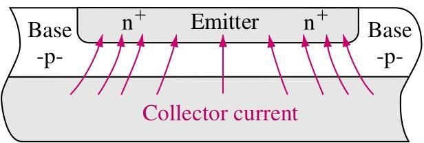
22 Base Sreading Resistance EB Junction is forward-biased Emitter ++ n Base Because of the base-sreading resistance, most of the hole injection occurs at the corners ollector Problematic with high-ower and high frequency devices. B Junction is reverse-biased 22
23 Emitter rowding in n BJT EB Junction is forward-biased Emitter ++ n Base ollector Emitter crowding at edges Problematic with high-ower and high frequency devices. B Junction is reverse-biased 23


24 Emitter rowding in nn BTT 24


25 Solution to Emitter rowding Since crowding occurs at edge, create base- and emitter connections with many edges 25

26 26
Radio Frequency Electronics
 Radio Frequency Electronics Active Components IV Samuel Morse Born in 79 in Massachusetts Fairly accomplished painter After witnessing various electrical experiments, got intrigued by electricity Designed
(11) Bipolar Op-Amp. Op-Amp Circuits:
 Bipolar Op-Amp. Op-Amp Circuits:") (11) O-Am Circuits: Biolar O-Am Learning Outcome Able to: Describe and analyze the dc and ac characteristics of the classic 741 biolar o-am circuit. eference: Neamen, Chater 13 11.0) 741 O-Am 11.1) Circuit
(11) O-Am Circuits: Biolar O-Am Learning Outcome Able to: Describe and analyze the dc and ac characteristics of the classic 741 biolar o-am circuit. eference: Neamen, Chater 13 11.0) 741 O-Am 11.1) Circuit
ESE 372 / Spring 2011 / Lecture 19 Common Base Biased by current source
 ESE 372 / Spring 2011 / Lecture 19 Common Base Biased by current source Output from Collector Start with bias DC analysis make sure BJT is in FA, then calculate small signal parameters for AC analysis.
Single-Stage BJT Amplifiers and BJT High-Frequency Model. Single-Stage BJT Amplifier Configurations
 1 Single-Stage BJT Amplifiers and BJT High-Frequency Model Asst. Prof. MONTREE SIRIPRUCHYANUN, D. Eng. Dept. of Teacher Training in Electrical Engineering, Faculty of Technical Education King Mongkut s
ESE319 Introduction to Microelectronics High Frequency BJT Model & Cascode BJT Amplifier
 High Frequency BJT Model & Cascode BJT Amplifier 1 Gain of 10 Amplifier Non-ideal Transistor C in R 1 V CC R 2 v s Gain starts dropping at > 1MHz. Why! Because of internal transistor capacitances that
Determining BJT SPICE Parameters
 Determining BJT SPICE Parameters Background Assume one wants to use SPICE to determine the frequency response for and for the amplifier below. Figure 1. Common-collector amplifier. After creating a schematic,
Bipolar Junction Transistor
 ESE 211 / Spring 2011 / Lecture 10 Bipolar Junction Transistor Let us first consider general transconductance amplifier loaded with short circuit Transconductance Obviously, power supplies are needed for
Bipolar Transistors. Ideal Transistor. Reading: (4-5 th edition) 8-16, Bipolar Transistor - Terminals. NPN Bipolar Transistor Physics
 8-16, Bipolar Transistor - Terminals. NPN Bipolar Transistor Physics") Bipolar Transistors deal Transistor Bipolar Transistor Terminals Reading: (45 th edition) 816, 2633 P Bipolar Transistor Physics Large Signal Model Early Effect Small Signal Model Modern Electronics: F3
Bipolar Transistors deal Transistor Bipolar Transistor Terminals Reading: (45 th edition) 816, 2633 P Bipolar Transistor Physics Large Signal Model Early Effect Small Signal Model Modern Electronics: F3
Chapter 4 DC Biasing BJTs. BJTs
 hapter 4 D Biasing BJTs BJTs Biasing Biasing: The D voltages applied to a transistor in order to turn it on so that it can amplify the A signal. Operating Point The D input establishes an operating or
Homework Assignment 05
 Homework Assignment 05 Question (2 points each unless otherwise indicated)(20 points). Estimate the parallel parasitic capacitance of a mh inductor with an SRF of 220 khz. Answer: (2π)(220 0 3 ) = ( 0
Last time: BJT CE and CB amplifiers biased by current source
 Last time: BJT CE and CB amplifiers biased by current source Assume FA regime, then VB VC V E I B I E, β 1 I Q C α I, V 0. 7V Calculate V CE and confirm it is > 0.2-0.3V, then BJT can be replaced with
BJT as an Amplifier and Its Biasing
 Microelectronic ircuits BJT as an Amplifier and Its Biasing Slide 1 Transfer haracteristics & Biasing Slide 2 BJT urrent-oltage relationship The collector current i I i i B s e i B vbe Is e T v BE T Emitter
dc Bias Point Calculations
 dc Bias Point Calculations Find all of the node voltages assuming infinite current gains 9V 9V 10kΩ 9V 100kΩ 1kΩ β = 270kΩ 10kΩ β = 1kΩ 1 dc Bias Point Calculations Find all of the node voltages assuming
Multistage Amplifiers
 Multistage Amplifiers Single-stage transistor amplifiers are inadequate for meeting most design requirements for any of the four amplifier types (voltage, current, transconductance, and transresistance.)
Physics of Bipolar Transistor
 Physics of Bipolar Transistor Motivations - In many electronic applications, amplifier is the most fundamental building block. Ex Audio amplifier: amplifies electric signal to drive a speaker RF Power
Lecture #7 BJT and JFET Frequency Response
 November 2014 Integrated Technical Education Cluster At AlAmeeria J-601-1448 Electronic Principals Lecture #7 BJT and JFET Frequency Response Instructor: Dr. Ahmad El-Banna Agenda Introduction General
Biasing. Biasing: The DC voltages applied to a transistor in order to turn it on so that it can amplify the AC signal.
 D iasing JT iasing iasing: The D voltages applied to a transistor in order to turn it on so that it can amplify the A signal. The D input establishes an operating or quiescent point called the Q-point.
The Miller Approximation. CE Frequency Response. The exact analysis is worked out on pp of H&S.
 CE Frequency Response The exact analysis is worked out on pp. 639-64 of H&S. The Miller Approximation Therefore, we consider the effect of C µ on the input node only V ---------- out V s = r g π m ------------------
CO2005: Electronics I. Transistor (BJT) Electronics I, Neamen 3th Ed. 1
 Electronics I, Neamen 3th Ed. 1") O2005: Electronics The Bipolar Junction Transistor (BJT) Electronics, Neamen 3th Ed. 1 Bipolar Transistor Structures N P 17 10 N D 19 10 N D 15 10 Electronics, Neamen 3th Ed. 2 Forward-Active Mode in the
O2005: Electronics The Bipolar Junction Transistor (BJT) Electronics, Neamen 3th Ed. 1 Bipolar Transistor Structures N P 17 10 N D 19 10 N D 15 10 Electronics, Neamen 3th Ed. 2 Forward-Active Mode in the
COMPARISON OF THE MOSFET AND THE BJT:
 COMPARISON OF THE MOSFET AND THE BJT: In this section we present a comparison of the characteristics of the two major electronic devices: the MOSFET and the BJT. To facilitate this comparison, typical
University of Southern C alifornia School Of Engineering Department Of Electrical Engineering
 University of Southern C alifornia School Of Engineering Department Of Electrical Engineering EE 348: Homework Assignment #04 Spring, 2001 (Due 02/27/2001) Choma Problem #16: n monolithic circuits, diodes
EE 434 Lecture 21. MOS Amplifiers Bipolar Devices
 434 ecture MOS Amplifiers ipolar Devices Quiz 3 The quiescent voltage across the 5K resistor in the circuit shown was measured to be 3. ) Determine the quiescent output voltage ) Determine the small signal
Week 12: Output Stages, Frequency Response
 ELE 2110A Electronic Circuits Week 12: Output Stages, Frequency esponse (2 hours only) Lecture 12-1 Output Stages Topics to cover Amplifier Frequency esponse eading Assignment: Chap 15.3, 16.1 of Jaeger
Chapter 4 Physics of Bipolar Transistors. EE105 - Spring 2007 Microelectronic Devices and Circuits. Structure and Symbol of Bipolar Transistor
 EE105 - Spring 2007 Microelectronic Devices and ircuits Lecture 10 Bipolar ransistors hapter 4 Physics of Bipolar ransistors 4.1 General onsiderations 4.2 Structure of Bipolar ransistor 4.3 Operation of
EEE225: Analogue and Digital Electronics
 EEE225: Analogue and Digital Electronics Lecture II James E. Green Department of Electronic Engineering University of Sheffield j.e.green@sheffield.ac.uk This Lecture 1 One Transistor Circuits Continued...
TO-92 SOT-23 Mark: 2A. TA = 25 C unless otherwise noted. Symbol Parameter Value Units
 2N396 / MMBT396 / MMPQ396 / PZT396 N Discrete POWER & Signal Technologies 2N396 MMBT396 E B E TO-92 SOT-23 Mark: 2A B MMPQ396 PZT396 E B E B E B E B SOI-6 SOT-223 B E This device is designed for general
University of Twente
 University of Twente Faculty of Electrical Engineering, Mathematics & Comuter Science Design of an audio ower amlifier with a notch in the outut imedance Remco Twelkemeijer MSc. Thesis May 008 Suervisors:
Homework Assignment 12
 Homework Assignment 12 Question 1 Shown the is Bode plot of the magnitude of the gain transfer function of a constant GBP amplifier. By how much will the amplifier delay a sine wave with the following
CHAPTER 3 THE BIPOLAR JUNCTION TRANSISTOR (BJT)
") HAPT 3 TH IPOLA JUNTION TANSISTO (JT) 1 In this chapter, we will: JT Discuss the physical structure and operation of the bipolar junction transistor. Understand the dc analysis of bipolar transistor circuits.
HAPT 3 TH IPOLA JUNTION TANSISTO (JT) 1 In this chapter, we will: JT Discuss the physical structure and operation of the bipolar junction transistor. Understand the dc analysis of bipolar transistor circuits.
การไบอ สทรานซ สเตอร. Transistors Biasing
 การไบอ สทรานซ สเตอร Transistors iasing iasing iasing: Applying D voltages to a transistor in order to turn it on so that it can amplify A signals. The D input establishes an operating or quiescent point
BJT Circuits (MCQs of Moderate Complexity)
") BJT Circuits (MCQs of Moderate Complexity) 1. The current ib through base of a silicon npn transistor is 1+0.1 cos (1000πt) ma. At 300K, the rπ in the small signal model of the transistor is i b B C r
BJT Circuits (MCQs of Moderate Complexity) 1. The current ib through base of a silicon npn transistor is 1+0.1 cos (1000πt) ma. At 300K, the rπ in the small signal model of the transistor is i b B C r
An Overview of Substrate Noise Reduction Techniques
 An Overview of Substrate Noise Reduction Techniques Shahab Ardalan, and Manoj Sachdev ardalan@ieee.org, msachdev@ece.uwaterloo.ca Deartment of Electrical and Comuter Engineering University of Waterloo
Building Blocks of Integrated-Circuit Amplifiers
 Building Blocks of ntegrated-circuit Amplifiers 1 The Basic Gain Cell CS and CE Amplifiers with Current Source Loads Current-source- or active-loaded CS amplifier Rin A o R A o g r r o g r 0 m o m o Current-source-
Lecture (06) Bipolar Junction Transistor
 Bipolar Junction Transistor") Lecture (06) Bipolar Junction Transistor By: Dr. Ahmed lshafee ١ Agenda BJT structure BJT operation BJT characteristics ٢ BJT structure The BJT is constructed with three doped semiconductor regions One
Lecture (06) Bipolar Junction Transistor By: Dr. Ahmed lshafee ١ Agenda BJT structure BJT operation BJT characteristics ٢ BJT structure The BJT is constructed with three doped semiconductor regions One
Switching threshold. Switch delay model. Input pattern effects on delay
 Switching threshold Low Power VLSI System Design Lecture 8 & 9: Transistor Sizing and Low Power Memory Design Prof. R. Iris ahar October & 4, 017 Define V M to be the oint where V in = V out (both PMOS
Lecture 4. Reading: Chapter EE105 Spring 2008 Lecture 4, Slide 2 Prof. Wu, UC Berkeley. Structure and Symbol of Bipolar Transistor
 Lecture 4 OULNE Bipolar Junction ransistor (BJ) General considerations Structure Operation in active mode Large signal model and characteristics ransconductance Small signal model he Early effect Reading:
Midterm 2 Exam. Max: 90 Points
 Midterm 2 Exam Name: Max: 90 Points Question 1 Consider the circuit below. The duty cycle and frequency of the 555 astable is 55% and 5 khz respectively. (a) Determine a value for so that the average current
Bipolar Junction Transistors (BJT)
") Bipolar Junction Transistors (BJT) deal Transistor Bipolar Transistor Terminals P Bipolar Transistor Physics Large Signal Model Early Effect Small Signal Model Reading: (Sedra, Smith, 7 th edition) 4.1
Bipolar Junction Transistors (BJT) deal Transistor Bipolar Transistor Terminals P Bipolar Transistor Physics Large Signal Model Early Effect Small Signal Model Reading: (Sedra, Smith, 7 th edition) 4.1
Bipolar Junction Transistors (BJTs) Overview
 Overview") 1 Bipolar Junction Transistors (BJTs) Asst. Prof. MONTREE SIRIPRUCHYANUN, D. Eng. Dept. of Teacher Training in Electrical Engineering, Faculty of Technical Education King Mongkut s Institute of Technology
1 Bipolar Junction Transistors (BJTs) Asst. Prof. MONTREE SIRIPRUCHYANUN, D. Eng. Dept. of Teacher Training in Electrical Engineering, Faculty of Technical Education King Mongkut s Institute of Technology
High-efficiency of MHz Inverter Constructed from Frequency Multiplying Circuit
 High-efficiency of MHz Inverter Constructed from Frequency Multilying Circuit Koji Orikawa, Jun-ichi Itoh Deartment of Electrical Engineering Nagaoka University of Technology Nagaoka, Jaan orikawa@vos.nagaokaut.ac.j
Lecture 6: Transistors Amplifiers. K.K. Gan Lecture 6: Transistors Amplifiers
 Lecture 6: Transistors Amplifiers ommon mitter Amplifier ( Simplified ): What's common (ground) a common emitter amp? The emitter! The emitter is connected (tied) to ground usually by a capacitor To an
6.976 High Speed Communication Circuits and Systems Lecture 5 High Speed, Broadband Amplifiers
 6.976 High Speed Communication Circuits and Systems Lecture 5 High Speed, Broadband Amplifiers Michael Perrott Massachusetts Institute of Technology Copyright 2003 by Michael H. Perrott Broadband Communication
UNIVERSITY OF CALIFORNIA AT BERKELEY College of Engineering Department of Electrical Engineering and Computer Sciences. Discussion Notes #9
 UNIVERSITY OF CALIFORNIA AT BERKELEY College of Engineering Department of Electrical Engineering and Computer Sciences Discussion Notes #9 EE 05 Spring 2007 Prof. Wu BJT Amplifiers Recall from Chapter
F7 Transistor Amplifiers
 Lars Ohlsson 2018-09-25 F7 Transistor Amplifiers Outline Transfer characteristics Small signal operation and models Basic configurations Common source (CS) CS/CE w/ source/ emitter degeneration resistance
D.C Biasing using a Single Power Supply
 4/6/0 D Biasing using a Single Power Supply /6 D. Biasing using a Single Power Supply The general form of a single-supply BJT amplifier biasing circuit is: - - Generally, we have three goals in designing
There are two basic types of FET s: The junction field effect transistor or JFET the metal oxide FET or MOSFET.
 Page 61 Field Effect Transistors The Fieldeffect transistor (FET) We know that the biolar junction transistor or BJT is a current controlled device. The FET or field effect transistor is a voltage controlled
Mini Project 2 Single Transistor Amplifiers. ELEC 301 University of British Columbia
 Mini Project 2 Single Transistor Amplifiers ELEC 301 University of British Columbia 44638154 October 27, 2017 Contents 1 Introduction 1 2 Investigation 1 2.1 Part 1.................................................
55:041 Electronic Circuits
 55:041 Electronic Circuits MOSFETs Sections of Chapter 3 &4 A. Kruger MOSFETs, Page-1 Basic Structure of MOS Capacitor Sect. 3.1 Width = 1 10-6 m or less Thickness = 50 10-9 m or less ` MOS Metal-Oxide-Semiconductor
BJT. Bipolar Junction Transistor BJT BJT 11/6/2018. Dr. Satish Chandra, Assistant Professor, P P N College, Kanpur 1
 BJT Bipolar Junction Transistor Satish Chandra Assistant Professor Department of Physics P P N College, Kanpur www.satish0402.weebly.com The Bipolar Junction Transistor is a semiconductor device which
Lecture #3 ( 2 weeks) Transistors
 Transistors") Spring 2015 Benha University Faculty of Engineering at Shoubra ECE-291 Electronic Engineering Lecture #3 ( 2 weeks) Transistors Instructor: Dr. Ahmad El-Banna 1 Agenda BJT Structure Basic Operation Transistor
Spring 2015 Benha University Faculty of Engineering at Shoubra ECE-291 Electronic Engineering Lecture #3 ( 2 weeks) Transistors Instructor: Dr. Ahmad El-Banna 1 Agenda BJT Structure Basic Operation Transistor
ET215 Devices I Unit 4A
 ITT Technical Institute ET215 Devices I Unit 4A Chapter 3, Section 3.1-3.2 This unit is divided into two parts; Unit 4A and Unit 4B Chapter 3 Section 3.1 Structure of Bipolar Junction Transistors The basic
Unit III FET and its Applications. 2 Marks Questions and Answers
 Unit III FET and its Applications 2 Marks Questions and Answers 1. Why do you call FET as field effect transistor? The name field effect is derived from the fact that the current is controlled by an electric
ITT Technical Institute. ET215 Devices 1. Unit 6 Chapter 3, Sections
 ITT Technical Institute ET215 Devices 1 Unit 6 Chapter 3, Sections 3.7-3.9 Chapter 3 Section 3.7 The Bipolar Transistor as a Switch Objectives: Explain how a transistor can be used as a switch 1. Compute
FINAL EXAMINATION SOLUTIONS
 FINAL EXAMINATION SOLUTIONS Electronics I for EE ourse Number EE 09-3 N 0460 Instructor: James K Beard, PhD beard@rowanedu Page of 3 Table of ontents Problem (0%)3 Solution 3 Problem (0%)5 Solution 6 Problem
Exercise 2: Collector Current Versus Base Current
 Exercise 2: Collector Current Versus Base Current EXERCISE OBJECTIVE When you have completed this exercise, you will be able to demonstrate the relationship of collector current to base current by using
Amplifier Frequency Response, Feedback, Oscillations; Op-Amp Block Diagram and Gain-Bandwidth Product
 Amplifier Frequency Response, Feedback, Oscillations; Op-Amp Block Diagram and Gain-Bandwidth Product Physics116A,12/4/06 Draft Rev. 1, 12/12/06 D. Pellett 2 Negative Feedback and Voltage Amplifier AB
6.012 Microelectronic Devices and Circuits
 Page 1 of 13 YOUR NAME Department of Electrical Engineering and Computer Science Massachusetts Institute of Technology 6.012 Microelectronic Devices and Circuits Final Eam Closed Book: Formula sheet provided;
5.25Chapter V Problem Set
 5.25Chapter V Problem Set P5.1 Analyze the circuits in Fig. P5.1 and determine the base, collector, and emitter currents of the BJTs as well as the voltages at the base, collector, and emitter terminals.
Chapter 3. Bipolar Junction Transistors
 Chapter 3. Bipolar Junction Transistors Outline: Fundamental of Transistor Common-Base Configuration Common-Emitter Configuration Common-Collector Configuration Introduction The transistor is a three-layer
Lecture 21: Voltage/Current Buffer Freq Response
 Lecture 21: Voltage/Current Buffer Freq Response Prof. Niknejad Lecture Outline Last Time: Frequency Response of Voltage Buffer Frequency Response of Current Buffer Current Mirrors Biasing Schemes Detailed
Lecture 14. Bipolar Junction Transistor (BJT) BJT 1-1
 BJT 1-1") Lecture 14 ipolar Junction Transistor (JT) JT 1-1 Outline ontinue JT iasing D analysis Fixed-bias circuit (revision) mitter-stabilized bias circuit oltage divider bias circuit D bias with voltage feedback
Lecture 14 ipolar Junction Transistor (JT) JT 1-1 Outline ontinue JT iasing D analysis Fixed-bias circuit (revision) mitter-stabilized bias circuit oltage divider bias circuit D bias with voltage feedback
Tutorial 2 BJTs, Transistor Bias Circuits, BJT Amplifiers FETs and FETs Amplifiers. Part 1: BJTs, Transistor Bias Circuits and BJT Amplifiers
 Tutorial 2 BJTs, Transistor Bias Circuits, BJT Amplifiers FETs and FETs Amplifiers Part 1: BJTs, Transistor Bias Circuits and BJT Amplifiers 1. Explain the purpose of a thin, lightly doped base region.
UNIVERSITY OF CALIFORNIA AT BERKELEY College of Engineering Department of Electrical Engineering and Computer Sciences.
 UNIVERSITY OF CALIFORNIA AT BERKELEY College of Engineering Department of Electrical Engineering and Computer Sciences Discussion #9 EE 05 Spring 2008 Prof. u MOSFETs The standard MOSFET structure is shown
EE 330 Lecture 16. Comparison of MOS Processes Bipolar Process
 330 Lecture 16 omparison of MOS Processes ipolar Process Review from last lecture P-Select Mask p-diffusion p-diffusion A-A Section Note the gate is self aligned!! - Section Review from last lecture n-select
EC2205 Electronic Circuits-1 UNIT III FREQUENCY RESPONSE OF AMPLIFIERS
 EC2205 Electronic Circuits-1 UNIT III FREQUENCY RESPONSE OF AMPLIFIERS PART A (2 MARK QUESTIONS) 1. Two amplifiers having gain 20 db and 40 db are cascaded. Find the overall gain in db. (NOV/DEC 2009)
8. Biasing Transistor Amplifiers
 8. iasing Transistor Amplifiers Lecture notes: Sec. 5 Sedra & Smith (6 th d): Sec. 5.4, 5.6 & 6.3-6.4 Sedra & Smith (5 th d): Sec. 4.4, 4.6 & 5.3-5.4 65, Winter013, F. Najmabadi ssues in developing a transistor
EE 435. Lecture 24. Offset Voltages Common Mode Feedback Circuits
 EE 435 Lecture 24 Offset Voltages Common Mode Feedback Circuits Review from last lecture Offset Voltage Two types of offset voltage: Systematic Offset Voltage Random Offset Voltage V OUT V ICQ fter fabrication
ES 330 Electronics II Homework # 1 (Fall 2016 SOLUTIONS)
") SOLUTIONS ES 330 Electronics II Homework # 1 (Fall 2016 SOLUTIONS) Problem 1 (20 points) We know that a pn junction diode has an exponential I-V behavior when forward biased. The diode equation relating
SOLUTIONS ES 330 Electronics II Homework # 1 (Fall 2016 SOLUTIONS) Problem 1 (20 points) We know that a pn junction diode has an exponential I-V behavior when forward biased. The diode equation relating
UNIT 3: FIELD EFFECT TRANSISTORS
 FIELD EFFECT TRANSISTOR: UNIT 3: FIELD EFFECT TRANSISTORS The field effect transistor is a semiconductor device, which depends for its operation on the control of current by an electric field. There are
Analog Electronics. Electronic Devices, 9th edition Thomas L. Floyd Pearson Education. Upper Saddle River, NJ, All rights reserved.
 Analog Electronics BJT Structure The BJT has three regions called the emitter, base, and collector. Between the regions are junctions as indicated. The base is a thin lightly doped region compared to the
ECE 442 Solid State Devices & Circuits. 15. Differential Amplifiers
 ECE 442 Solid State Devices & Circuits 15. Differential Amplifiers Jose E. Schutt-Aine Electrical & Computer Engineering University of Illinois jschutt@emlab.uiuc.edu ECE 442 Jose Schutt Aine 1 Background
Bipolar Junction Transistors
 ipolar Junction Transistor (JT ipolar Junction Transistors JT is a three-terminal device: emitter (, collector ( and base (. There are two types: pnp-type and npn-type. npn transistor: emitter & collector
! PN Junction. ! MOS Transistor Topology. ! Threshold. ! Operating Regions. " Resistive. " Saturation. " Subthreshold (next class)
") ESE370: ircuit-level Modeling, Design, and Optimization for Digital Systems Today! PN Junction! MOS Transistor Topology! Threshold Lec 7: September 16, 2015 MOS Transistor Operating Regions Part 1! Operating
ESE370: ircuit-level Modeling, Design, and Optimization for Digital Systems Today! PN Junction! MOS Transistor Topology! Threshold Lec 7: September 16, 2015 MOS Transistor Operating Regions Part 1! Operating
TO-92 SOT-23 Mark: 83. TA = 25 C unless otherwise noted. Symbol Parameter Value Units
 2N44 MMBT44 2N44 / MMBT44 B E TO-92 SOT-23 Mark: 83 B E This device is designed for use as general purpose amplifiers and switches requiring collector currents to 5 ma. Absolute Maximum Ratings* TA = 25
Preliminary Exam, Fall 2013 Department of Electrical and Computer Engineering University of California, Irvine EECS 170B
 Preliminary Exam, Fall 2013 Department of Electrical and Computer Engineering University of California, Irvine EECS 170B Problem 1. Consider the following circuit, where a saw-tooth voltage is applied
UNIT-1 Bipolar Junction Transistors. Text Book:, Microelectronic Circuits 6 ed., by Sedra and Smith, Oxford Press
 UNIT-1 Bipolar Junction Transistors Text Book:, Microelectronic Circuits 6 ed., by Sedra and Smith, Oxford Press Figure 6.1 A simplified structure of the npn transistor. Microelectronic Circuits, Sixth
MOS Field-Effect Transistors (MOSFETs)
") 6 MOS Field-Effect Transistors (MOSFETs) A three-terminal device that uses the voltages of the two terminals to control the current flowing in the third terminal. The basis for amplifier design. The basis
6 MOS Field-Effect Transistors (MOSFETs) A three-terminal device that uses the voltages of the two terminals to control the current flowing in the third terminal. The basis for amplifier design. The basis
Lecture 3: Transistors
 Lecture 3: Transistors Now that we know about diodes, let s put two of them together, as follows: collector base emitter n p n moderately doped lightly doped, and very thin heavily doped At first glance,
EE105 Fall 2015 Microelectronic Devices and Circuits
 EE105 Fall 2015 Microelectronic Devices and Circuits Prof. Ming C. Wu wu@eecs.berkeley.edu 511 Sutardja Dai Hall (SDH) 11-1 Transistor Operating Mode in Amplifiers Transistors are biased in flat part of
Chapter 7: Passive Filters
 EETOMAGNETI OMPATIBIITY HANDBOOK 1 hater 7: Passive Filters 7.1 eeat the analytical analysis given in this chater for the low-ass filter for an filter in shunt with the load. The and for this filter are
Electronic Circuits Laboratory EE462G Lab #8. BJT Common Emitter Amplifier
 lectronic ircuits Laboratory 46G Lab #8 JT ommon mitter Amplifier npn ipolar Junction Transistor JT in a common-emitter configuration ase ollector V _ n p n V _ mitter For most applications the JT is operated
Analog Integrated Circuit Design Exercise 1
 Analog Integrated Circuit Design Exercise 1 Integrated Electronic Systems Lab Prof. Dr.-Ing. Klaus Hofmann M.Sc. Katrin Hirmer, M.Sc. Sreekesh Lakshminarayanan Status: 21.10.2015 Pre-Assignments The lecture
Current Mirrors. Prof. Tai-Haur Kuo, EE, NCKU, Tainan City, Taiwan 4-1
 Current Mirrors Prof. Tai-Haur Kuo, EE, NCKU, Tainan City, Taiwan 4- 郭泰豪, Analog C Design, 08 { Prof. Tai-Haur Kuo, EE, NCKU, Tainan City, Taiwan 4- 郭泰豪, Analog C Design, 08 { Current Source and Sink Symbol
T- filters based dual-control dimmable electronic ballast
 3rd International Conference on Mechatronics, obotics and Automation (ICMA 5 T- filters based dual-control dimmable electronic ballast Huadong Wang, a,xu Cai, b,lili Liu Electronic Information and Electrical
Chapter 6. BJT Amplifiers
 Basic Electronic Devices and Circuits EE 111 Electrical Engineering Majmaah University 2 nd Semester 1432/1433 H Chapter 6 BJT Amplifiers 1 Introduction The things you learned about biasing a transistor
55:041 Electronic Circuits
 55:041 Electronic Circuits Mosfet Review Sections of Chapter 3 &4 A. Kruger Mosfet Review, Page-1 Basic Structure of MOS Capacitor Sect. 3.1 Width 1 10-6 m or less Thickness 50 10-9 m or less ` MOS Metal-Oxide-Semiconductor
1.2 Power MOSFET and IGBT
 Most alications for currents of some 10A use transistors with silicon chis that are integrated in otentialfree ower modules. These modules contain one or several transistor systems, diodes adated to the
Chapter 3 Bipolar Junction Transistors (BJT)
") Chapter 3 Bipolar Junction Transistors (BJT) Transistors In analog circuits, transistors are used in amplifiers and linear regulated power supplies. In digital circuits they function as electrical switches,
Chapter 3 Bipolar Junction Transistors (BJT) Transistors In analog circuits, transistors are used in amplifiers and linear regulated power supplies. In digital circuits they function as electrical switches,
SYLLABUS OSMANIA UNIVERSITY (HYDERABAD)
") UNIT - 1 i SYLLABUS OSMANIA UNIVERSITY (HYDERABAD) JUNCTION DIODE Different Types of PN Junction Formation Techniques, PN Junction Characteristics, Biasing, Band Diagrams and Current Flow, Diode Current
UNIT - 1 i SYLLABUS OSMANIA UNIVERSITY (HYDERABAD) JUNCTION DIODE Different Types of PN Junction Formation Techniques, PN Junction Characteristics, Biasing, Band Diagrams and Current Flow, Diode Current
(a) BJT-OPERATING MODES & CONFIGURATIONS
 BJT-OPERATING MODES & CONFIGURATIONS") (a) BJT-OPERATING MODES & CONFIGURATIONS 1. The leakage current I CBO flows in (a) The emitter, base and collector leads (b) The emitter and base leads. (c) The emitter and collector leads. (d) The base
(a) BJT-OPERATING MODES & CONFIGURATIONS 1. The leakage current I CBO flows in (a) The emitter, base and collector leads (b) The emitter and base leads. (c) The emitter and collector leads. (d) The base
UNIVERSITY PART-B ANSWERS UNIT-1
 UNERSTY PART-B ANSWERS UNT-. Discuss about the DC load line and Q point. (OR) What is D.C. load line, how will you select the operating point, explain it using common emitter amplifier characteristics
Field-Effect Transistor (FET) is one of the two major transistors; FET derives its name from its working mechanism;
 is one of the two major transistors; FET derives its name from its working mechanism;") Chapter 3 Field-Effect Transistors (FETs) 3.1 Introduction Field-Effect Transistor (FET) is one of the two major transistors; FET derives its name from its working mechanism; The concept has been known
Chapter 3 Field-Effect Transistors (FETs) 3.1 Introduction Field-Effect Transistor (FET) is one of the two major transistors; FET derives its name from its working mechanism; The concept has been known
Transistors. Bipolar Junction transistors Principle of operation Characteristics. Field effect transistors Principle of operation Characteristics
 Transistors ipolar Junction transistors Principle of operation haracteristics Field effect transistors Principle of operation haracteristics ntroduction Radio based on vacuum tubes Fundamental building
THE METAL-SEMICONDUCTOR CONTACT
 THE METAL-SEMICONDUCTOR CONTACT PROBLEM 1 To calculate the theoretical barrier height, built-in potential barrier, and maximum electric field in a metal-semiconductor diode for zero applied bias. Consider
Basic Electronics Prof. Dr. Chitralekha Mahanta Department of Electronics and Communication Engineering Indian Institute of Technology, Guwahati
 Basic Electronics Prof. Dr. Chitralekha Mahanta Department of Electronics and Communication Engineering Indian Institute of Technology, Guwahati Module: 2 Bipolar Junction Transistors Lecture-1 Transistor
ESE319 Introduction to Microelectronics BJT Intro and Large Signal Model
 BJT Intro and Large Signal Model 1 VLSI Chip Manufacturing Process 2 0.35 mm SiGe BiCMOS Layout for RF (3.5 GHz) Two-Stage Power Amplifier Each transistor above is realized as net of four heterojunction
Single-Stage Integrated- Circuit Amplifiers
 Single-Stage Integrated- Circuit Amplifiers Outline Comparison between the MOS and the BJT From discrete circuit to integrated circuit - Philosophy, Biasing, etc. Frequency response The Common-Source and
TO-92 SOT-23 Mark: 3G. TA = 25 C unless otherwise noted. Symbol Parameter Value Units
 MPSH MMBTH MPSH / MMBTH E B TO-92 SOT-2 Mark: G B E This device is designed for common-emitter low noise amplifier and mixer applications with collector currents in the µa to ma range to MHz, and low frequency
Radio Frequency Electronics
 Radio Frequency Electronics Active Components II Harry Nyquist Born in 1889 in Sweden Received B.S. and M.S. from U. North Dakota Received Ph.D. from Yale Worked and Bell Laboratories for all of his career
DIGITALLY CONTROLLED QUADRATURE OSCILLATOR EMPLOYING TWO ZC-CG-CDBAs
 DIGITALLY ONTOLLED QUADATUE OSILLATO EMPLOYING TWO Z-G-DBAs Josef Bajer, Dalibor Biolek UD/BUT, Det. of EE/Microelectronics Kounicova 65/Udolni 53, Brno, zech eublic dalibor.biolek@unob.cz ABSTAT: A simle