Biasing. Biasing: The DC voltages applied to a transistor in order to turn it on so that it can amplify the AC signal.
|
|
|
- Godfrey Black
- 5 years ago
- Views:
Transcription
1 D iasing JT
2 iasing iasing: The D voltages applied to a transistor in order to turn it on so that it can amplify the A signal.
3 The D input establishes an operating or quiescent point called the Q-point. Operating Point
4 The Three States of Operation Active or Linear egion Operation ase mitter junction is forward biased ase ollector junction is reverse biased utoff egion Operation ase mitter junction is reverse biased Saturation egion Operation ase mitter junction is forward biased ase ollector junction is forward biased
5 D iasing ircuits Fixed-bias circuit mitter-stabilized bias circuit oltage divider bias circuit D bias with voltage feedback mitter Follower configuration ommon base configuration
6 Fixed ias
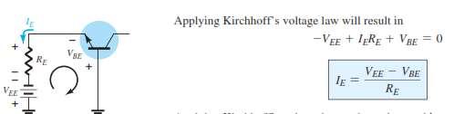
7 The ase-mitter Loop From Kirchhoff s voltage law: + = 0 Solving for base current:
8 ollector-mitter Loop ollector current: From Kirchhoff s voltage law:
9 Transistor Saturation When the transistor is operating in saturation, current through the transistor is at its maximum possible value. sat 0
10 The end points of the load line are: sat = / Load Line Analysis = 0 cutoff = = 0 ma The Q-point is the operating point: where the value of sets the value of that sets the values of and
11 ircuit alues Affect the Q-Point more


12 ircuit alues Affect the Q-Point more
13 ircuit alues Affect the Q-Point
14 mitter-stabilized ias ircuit Adding a resistor ( ) to the emitter circuit stabilizes the bias circuit.
15 ase-mitter Loop From Kirchhoff s voltage law: Since = ( + 1) : ( 1) 0 Solving for : - ( 1)
16 ollector-mitter Loop From Kirchhoff s voltage law: 0 Since : ( ) Also: -
17 mproved iased Stability Stability refers to a circuit condition in which the currents and voltages will remain fairly constant over a wide range of temperatures and transistor eta () values. Adding to the emitter improves the stability of a transistor.
18 Saturation Level The endpoints can be determined from the load line. cutoff : sat : 0 ma 0
19 oltage Divider ias This is a very stable bias circuit. The currents and voltages are nearly independent of any variations in.

20 xact Analysis

21 xact Analysis (cont.)
22 Approximate Analysis Where << 1 and 1 2 : Where > 10 2 : From Kirchhoff s voltage law: ) (
23 oltage Divider ias Analysis Transistor Saturation Level sat max Load Line Analysis utoff: 0mA Saturation: 0
24 D ias with oltage Feedback/ ollector Feedback onfiguration Another way to improve the stability of a bias circuit is to add a feedback path from collector to base. n this bias circuit the Q-point is only slightly dependent on the transistor beta,.
25 From Kirchhoff s voltage law: ase-mitter Loop 0 Where << : ' Knowing = and, the loop equation becomes: 0 Solving for : ( )
26 ollector-mitter Loop Applying Kirchoff s voltage law: + + = 0 Since and = : ( + ) + =0 Solving for : = ( + )
27 Saturation Analysis Transistor Saturation Level sat max Load Line Analysis utoff: 0 ma Saturation: 0
28 mitter follower onfiguration oltage is taken off from collector Saturation:

29 mitter follower onfiguration (cont.)
30 ommon ase onfiguration
31 ommon ase onfiguration (cont.)
32 Design Problem xample
33 Design Problem: Solution
34 Transistor Switching Networks Transistors with only the D source applied can be used as electronic switches. Transistors as inverters
35 i = 5 Saturation current: sat To ensure saturation: Switching ircuit alculations sat dc
36 i= 0
37 mitter-collector resistance at saturation and cutoff: sat sat sat cutoff O
38 Switching Time Transistor switching times: t on t r t d t off t s t f t r td ise time 10% to 90% Delay time t s t f Storage time Fall time 90% to 10%
39 PNP Transistors The analysis for pnp transistor biasing circuits is the same as that for npn transistor circuits. The only difference is that the currents are flowing in the opposite direction.
 ase-emitter loop")
40 PNP Transistors (cont.) ase-emitter loop ollector-emitter loop
41 Troubleshooting Hints Approximate voltages.7 for silicon transistors 25% to 75% of Test for opens and shorts with an ohmmeter. Test the solder joints. Test the transistor with a transistor tester or a curve tracer. Note that the load or the next stage affects the transistor operation.
การไบอ สทรานซ สเตอร. Transistors Biasing
 การไบอ สทรานซ สเตอร Transistors iasing iasing iasing: Applying D voltages to a transistor in order to turn it on so that it can amplify A signals. The D input establishes an operating or quiescent point
Chapter 4 DC Biasing BJTs. BJTs
 hapter 4 D Biasing BJTs BJTs Biasing Biasing: The D voltages applied to a transistor in order to turn it on so that it can amplify the A signal. Operating Point The D input establishes an operating or
Lecture 9. Bipolar Junction Transistor (BJT) BJT 1-1
 BJT 1-1") Lecture 9 ipolar Junction Transistor (JT) JT 1-1 Outline ontinue JT JT iasing D analysis Fixed-bias circuit mitter-stabilized bias circuit oltage divider bias circuit D bias with voltage feedback circuit
Lecture 9 ipolar Junction Transistor (JT) JT 1-1 Outline ontinue JT JT iasing D analysis Fixed-bias circuit mitter-stabilized bias circuit oltage divider bias circuit D bias with voltage feedback circuit
Lecture 14. Bipolar Junction Transistor (BJT) BJT 1-1
 BJT 1-1") Lecture 14 ipolar Junction Transistor (JT) JT 1-1 Outline ontinue JT iasing D analysis Fixed-bias circuit (revision) mitter-stabilized bias circuit oltage divider bias circuit D bias with voltage feedback
Lecture 14 ipolar Junction Transistor (JT) JT 1-1 Outline ontinue JT iasing D analysis Fixed-bias circuit (revision) mitter-stabilized bias circuit oltage divider bias circuit D bias with voltage feedback
CHAPTER 3 THE BIPOLAR JUNCTION TRANSISTOR (BJT)
") HAPT 3 TH IPOLA JUNTION TANSISTO (JT) 1 In this chapter, we will: JT Discuss the physical structure and operation of the bipolar junction transistor. Understand the dc analysis of bipolar transistor circuits.
HAPT 3 TH IPOLA JUNTION TANSISTO (JT) 1 In this chapter, we will: JT Discuss the physical structure and operation of the bipolar junction transistor. Understand the dc analysis of bipolar transistor circuits.
Session 4: Analog Circuits. BJT Biasing Single stage amplifier
 Session 4: Analog ircuits JT iasing Single stage amplifier 1 Outline JT Amplifier 2 JT: ipolar Junction Transistor i D A p D n R F F : Forward R : Reverse V D p n p n p n 1 2 1 : F 2 : R Active V 1 : F
fiziks Institute for NET/JRF, GATE, IIT-JAM, M.Sc. Entrance, JEST, TIFR and GRE in Physics
 nstitute for NT/JF, GAT, T-JAM, M.Sc. ntrance, JST, TF and G in Physics 3. ipolar Junction Transistors 3.1 Transistor onstruction Transistor is a three-layer semiconductor device consisting of either two
Electronic Devices, 9th edition Thomas L. Floyd. Input signal. R 1 and R 2 are selected to establish V B. If the V CE
 3/9/011 lectronic Devices Ninth dition Floyd hapter 5: Transistor ias ircuits The D Operating Point ias establishes the operating point (Q-point) of a transistor amplifier; the ac signal (ma) moves above
Electronics Fundamentals BIPOLAR TRANSISTORS. Construction, circuit symbols and biasing examples for NPN and PNP junction transistors.
 IPOLA TANSISTOS onstruction, circuit symbols and biasing examples for NPN and PNP junction transistors Slide 1 xternal bias voltages create an electric field, which pulls electrons (emitted into the base
Lecture (06) Bipolar Junction Transistor
 Bipolar Junction Transistor") Lecture (06) Bipolar Junction Transistor By: Dr. Ahmed lshafee ١ Agenda BJT structure BJT operation BJT characteristics ٢ BJT structure The BJT is constructed with three doped semiconductor regions One
Lecture (06) Bipolar Junction Transistor By: Dr. Ahmed lshafee ١ Agenda BJT structure BJT operation BJT characteristics ٢ BJT structure The BJT is constructed with three doped semiconductor regions One
Celso José Faria de Araújo, M.Sc.
 elso José Faria de Araújo, M.Sc. TH IPOLA JUNTION TANSISTOS - JT Objecties: Understand the basic principles of JT operation Interpret the transport model Identify operating regions of the JT and use simplified
Lecture (08) Bipolar Junction Transistor (2)
 Bipolar Junction Transistor (2)") Lecture (08) ipolar Junction Transistor (2) y: Dr. Ahmed lshafee 1 JT haracteristic ollector haracteristic urves 2 Applying fixed V, increasing V Saturation Assume that V is set to produce a certain value
Lecture (08) ipolar Junction Transistor (2) y: Dr. Ahmed lshafee 1 JT haracteristic ollector haracteristic urves 2 Applying fixed V, increasing V Saturation Assume that V is set to produce a certain value
Electronic Circuits Laboratory EE462G Lab #8. BJT Common Emitter Amplifier
 lectronic ircuits Laboratory 46G Lab #8 JT ommon mitter Amplifier npn ipolar Junction Transistor JT in a common-emitter configuration ase ollector V _ n p n V _ mitter For most applications the JT is operated
BJT as an Amplifier and Its Biasing
 Microelectronic ircuits BJT as an Amplifier and Its Biasing Slide 1 Transfer haracteristics & Biasing Slide 2 BJT urrent-oltage relationship The collector current i I i i B s e i B vbe Is e T v BE T Emitter
CO2005: Electronics I. Transistor (BJT) Electronics I, Neamen 3th Ed. 1
 Electronics I, Neamen 3th Ed. 1") O2005: Electronics The Bipolar Junction Transistor (BJT) Electronics, Neamen 3th Ed. 1 Bipolar Transistor Structures N P 17 10 N D 19 10 N D 15 10 Electronics, Neamen 3th Ed. 2 Forward-Active Mode in the
O2005: Electronics The Bipolar Junction Transistor (BJT) Electronics, Neamen 3th Ed. 1 Bipolar Transistor Structures N P 17 10 N D 19 10 N D 15 10 Electronics, Neamen 3th Ed. 2 Forward-Active Mode in the
Bipolar Junction Transistors
 ipolar Junction Transistor (JT ipolar Junction Transistors JT is a three-terminal device: emitter (, collector ( and base (. There are two types: pnp-type and npn-type. npn transistor: emitter & collector
FYSE400 ANALOG ELECTRONICS
 7.9.016 YS400 ANALOG LTONS LTU 1 ntroduction to ipolar Junction Transistor ircuits 1 NTODUTON The deal urrent-controlled urrent Source efore the detailed analyzation of transistor operation, we should
Biasing of BJT IENGINEERS- CONSULTANTS LECTURE NOTES SERIES ELECTRONICS ENGINEERING 1 YEAR UPTU. Page 1
 HTTP://NGNS.N/ NGNS- ONSULTANTS LTU NOTS SS LTONS NGNNG 1 YA UPTU iasing of JT As we know that JT can be operated in three regions: active, saturation and cutoff by applying proper voltage condition. n
The first transistor. (Courtesy Bell Telephone Laboratories.)
") Fig. 3.1 The first transistor. (Courtesy Bell Telephone Laboratories.) Fig. 3.2 Types of transistors: (a) pnp; (b) npn. : (a) pnp; : (b) npn Fig. 3.3 Forward-biased junction of a pnp transistor. Fig. 3.4
Fig. 3.1 The first transistor. (Courtesy Bell Telephone Laboratories.) Fig. 3.2 Types of transistors: (a) pnp; (b) npn. : (a) pnp; : (b) npn Fig. 3.3 Forward-biased junction of a pnp transistor. Fig. 3.4
8. Biasing Transistor Amplifiers
 8. iasing Transistor Amplifiers Lecture notes: Sec. 5 Sedra & Smith (6 th d): Sec. 5.4, 5.6 & 6.3-6.4 Sedra & Smith (5 th d): Sec. 4.4, 4.6 & 5.3-5.4 65, Winter013, F. Najmabadi ssues in developing a transistor
Chapter 3: Bipolar Junction Transistors
 Chapter 3: Bipolar Junction Transistors Transistor Construction There are two types of transistors: pnp npn pnp The terminals are labeled: E - Emitter B - Base C - Collector npn 2 Transistor Operation
Transistors as Amplifiers
 Transistors as Amplifiers The transistor works in the active region (a F ) around the quiescent point QP dc supply (dc voltage sources, dc current sources) asic amplifier with one transistor: S and amplifiers
Lecture #3 BJT Transistors & DC Biasing
 November 2014 Ahmad El-Banna Integrated Technical Education Cluster At AlAmeeria J-601-1448 Electronic Principals Lecture #3 BJT Transistors & DC Biasing Instructor: Dr. Ahmad El-Banna Agenda Transistor
DC Bias. Graphical Analysis. Script
 Course: B.Sc. Applied Physical Science (Computer Science) Year & Sem.: Ist Year, Sem - IInd Subject: Electronics Paper No.: V Paper Title: Analog Circuits Lecture No.: 3 Lecture Title: Analog Circuits
Introduction PNP C NPN C
 Introduction JT Transistors: A JT (or any transistor) can be used either as a switch with positions of on or off, or an amplifier that controls its output at all levels in between the extreme on or off
Chapter 5 Transistor Bias Circuits
 Chapter 5 Transistor Bias Circuits Objectives Discuss the concept of dc biasing of a transistor for linear operation Analyze voltage-divider bias, base bias, and collector-feedback bias circuits. Basic
I C I E =I B = I C 1 V BE 0.7 V
 Guide to NPN Amplifier Analysis Jason Woytowich 1. Transistor characteristics A BJT has three operating modes cutoff, active, and saturation. For applications, like amplifiers, where linear characteristics
Lecture 6. OUTLINE BJT (cont d) PNP transistor (structure, operation, models) BJT Amplifiers General considerations. Reading: Chapter
 PNP transistor (structure, operation, models) BJT Amplifiers General considerations. Reading: Chapter") Lecture 6 ANNOUNCMNTS HW#3, Prob. 2: Re-draw -plots for W reduced by a factor of 2. n case of a major earthquake: Try to duck/crouch on the floor in front of the seats for cover. Once the earthquake stops,
Lecture 6 ANNOUNCMNTS HW#3, Prob. 2: Re-draw -plots for W reduced by a factor of 2. n case of a major earthquake: Try to duck/crouch on the floor in front of the seats for cover. Once the earthquake stops,
Lecture 6: Transistors Amplifiers. K.K. Gan Lecture 6: Transistors Amplifiers
 Lecture 6: Transistors Amplifiers ommon mitter Amplifier ( Simplified ): What's common (ground) a common emitter amp? The emitter! The emitter is connected (tied) to ground usually by a capacitor To an
Analog Electronics (Course Code: EE314) Lecture 5 7: Junction contd, BJT. Course Instructor: Shree Prakash Tiwari
 Lecture 5 7: Junction contd, BJT. Course Instructor: Shree Prakash Tiwari") ndian nstitute of echnology Jodhpur, Year 2017 Analog lectronics (ourse ode: 314) Lecture 5 7: Junction contd, J ourse nstructor: Shree Prakash iwari mail: sptiwari@iitj.ac.in Webpage: http://home.iitj.ac.in/~sptiwari/
ndian nstitute of echnology Jodhpur, Year 2017 Analog lectronics (ourse ode: 314) Lecture 5 7: Junction contd, J ourse nstructor: Shree Prakash iwari mail: sptiwari@iitj.ac.in Webpage: http://home.iitj.ac.in/~sptiwari/
Exercise 2: AC Voltage and Power Gains
 Exercise 2: AC Voltage and Power Gains When you have completed this exercise, you will be able to determine voltage and power gains by using oscilloscope. The ac operation schematic for the COMPLEMENTARY
EXPERIMENT 12: SIMULATION STUDY OF DIFFERENT BIASING CIRCUITS USING NPN BJT
 EXPERIMENT 12: SIMULATION STUDY OF DIFFERENT BIASING CIRCUITS USING NPN BJT AIM: 1) To study different BJT DC biasing circuits 2) To design voltage divider bias circuit using NPN BJT SOFTWARE TOOL: PC
ET215 Devices I Unit 4A
 ITT Technical Institute ET215 Devices I Unit 4A Chapter 3, Section 3.1-3.2 This unit is divided into two parts; Unit 4A and Unit 4B Chapter 3 Section 3.1 Structure of Bipolar Junction Transistors The basic
Transistors. electrons N P N holes. Base. An NPN device makes a transistor
 NPN Transistor Theory Transistors Transistors are similar to diodes in that they are made up on ntype and ptype silicon. They differ in that Transistors are 3terminal devices (NPN or PNP), Transistors
Laboratory Four - Bipolar Junction Transistor (BJT)
") M/IS 3512 ioelectronics Laboratory Four - ipolar Junction Transistor (JT) Learning Objectives: Know how to differentiate between PNP & NPN JT transistors using a multimeter. e familiar with the operation
M/IS 3512 ioelectronics Laboratory Four - ipolar Junction Transistor (JT) Learning Objectives: Know how to differentiate between PNP & NPN JT transistors using a multimeter. e familiar with the operation
Chapter 4 Physics of Bipolar Transistors. EE105 - Spring 2007 Microelectronic Devices and Circuits. Structure and Symbol of Bipolar Transistor
 EE105 - Spring 2007 Microelectronic Devices and ircuits Lecture 10 Bipolar ransistors hapter 4 Physics of Bipolar ransistors 4.1 General onsiderations 4.2 Structure of Bipolar ransistor 4.3 Operation of
Chapter 3. Bipolar Junction Transistors
 Chapter 3. Bipolar Junction Transistors Outline: Fundamental of Transistor Common-Base Configuration Common-Emitter Configuration Common-Collector Configuration Introduction The transistor is a three-layer
Chapter 3 Bipolar Junction Transistors (BJT)
") Chapter 3 Bipolar Junction Transistors (BJT) Transistors In analog circuits, transistors are used in amplifiers and linear regulated power supplies. In digital circuits they function as electrical switches,
Chapter 3 Bipolar Junction Transistors (BJT) Transistors In analog circuits, transistors are used in amplifiers and linear regulated power supplies. In digital circuits they function as electrical switches,
EE 434 Lecture 21. MOS Amplifiers Bipolar Devices
 434 ecture MOS Amplifiers ipolar Devices Quiz 3 The quiescent voltage across the 5K resistor in the circuit shown was measured to be 3. ) Determine the quiescent output voltage ) Determine the small signal
Università degli Studi di Roma Tor Vergata Dipartimento di Ingegneria Elettronica. Analogue Electronics. Paolo Colantonio A.A.
 Università degli Studi di Roma Tor Vergata Dipartimento di Ingegneria Elettronica Analogue Electronics Paolo olantonio A.A. 2015-16 ias issues The D bias point is affected by thermal issue due to the active
Electrical, Electronic and Digital Principles (EEDP) Lecture 3. Other BJT Biasing Techniques باسم ممدوح الحلوانى
 Lecture 3. Other BJT Biasing Techniques باسم ممدوح الحلوانى") Electrical, Electronic and Digital Principles (EEDP) Lecture 3 Other BJT Biasing Techniques د. باسم ممدوح الحلوانى Approximate Analysis Voltage-divider Bias Exact Analysis Ri = is the equivalent resistance
Electrical, Electronic and Digital Principles (EEDP) Lecture 3 Other BJT Biasing Techniques د. باسم ممدوح الحلوانى Approximate Analysis Voltage-divider Bias Exact Analysis Ri = is the equivalent resistance
Current Mirrors. Basic BJT Current Mirror. Current mirrors are basic building blocks of analog design. Figure shows the basic NPN current mirror.
 Current Mirrors Basic BJT Current Mirror Current mirrors are basic building blocks of analog design. Figure shows the basic NPN current mirror. For its analysis, we assume identical transistors and neglect
EE 330 Lecture 18. Characteristics of Finer Feature Size Processes. Bipolar Process
 330 Lecture 18 haracteristics of Finer Feature Size Processes ipolar Process How does the inverter delay compare between a 0.5u process and a 0.13u process? DD IN OUT IN OUT SS How does the inverter
I B. VCE =const. 25mV I C. V out = I C R C = β I B R C = βr C βr e
 Physics 338 L 6 Spring 2016 ipolar Junction Transistors 0. (a) Load Lines and haracteristic urves The below figure shows the characteristic curves for a JT along with the load line for the simple common
ELEC 2210 EXPERIMENT 7 The Bipolar Junction Transistor (BJT)
") ELEC 2210 EXPERIMENT 7 The Bipolar Junction Transistor (BJT) Objectives: The experiments in this laboratory exercise will provide an introduction to the BJT. You will use the Bit Bucket breadboarding system
ELEC 2210 EXPERIMENT 7 The Bipolar Junction Transistor (BJT) Objectives: The experiments in this laboratory exercise will provide an introduction to the BJT. You will use the Bit Bucket breadboarding system
ITT Technical Institute. ET215 Devices 1. Unit 6 Chapter 3, Sections
 ITT Technical Institute ET215 Devices 1 Unit 6 Chapter 3, Sections 3.7-3.9 Chapter 3 Section 3.7 The Bipolar Transistor as a Switch Objectives: Explain how a transistor can be used as a switch 1. Compute
Lecture 24: Bipolar Junction Transistors (1) Bipolar Junction Structure, Operating Regions, Biasing
 Bipolar Junction Structure, Operating Regions, Biasing") Lecture 24: Bipolar Junction Transistors (1) Bipolar Junction Structure, Operating Regions, Biasing BJT Structure the BJT is formed by doping three semiconductor regions (emitter, base, and collector)
Lecture 24: Bipolar Junction Transistors (1) Bipolar Junction Structure, Operating Regions, Biasing BJT Structure the BJT is formed by doping three semiconductor regions (emitter, base, and collector)
Transistors and Applications
 Chapter 17 Transistors and Applications DC Operation of Bipolar Junction Transistors (BJTs) The bipolar junction transistor (BJT) is constructed with three doped semiconductor regions separated by two
Transistor Configuration
 Transistor Configuration 1 Objectives To review BJT biasing circuit. To study BJT amplifier circuit To understand the BJT configuration. To analyse single-stage BJT amplifier circuits. To study the differential
Chapter 2. Bipolar Junction Transistor
 Chapter 2 ipolar Junction Transistor 2.0 History The name bipolar is used because both types of carriers namely hole and electron are used in the transistor, as opposed to field effect transistor, which
Electrical, Electronic and Digital Principles (EEDP) Lecture 3. Other BJT Biasing Techniques باسم ممدوح الحلوانى
 Lecture 3. Other BJT Biasing Techniques باسم ممدوح الحلوانى") Electrical, Electronic and Digital Principles (EEDP) Lecture 3 Other BJT Biasing Techniques د. باسم ممدوح الحلوانى Approximate Analysis Voltage-divider Bias Exact Analysis Ri = is the equivalent resistance
Electrical, Electronic and Digital Principles (EEDP) Lecture 3 Other BJT Biasing Techniques د. باسم ممدوح الحلوانى Approximate Analysis Voltage-divider Bias Exact Analysis Ri = is the equivalent resistance
Transistor Biasing. DC Biasing of BJT. Transistor Biasing. Transistor Biasing 11/23/2018
 Transistor Biasing DC Biasing of BJT Satish Chandra Assistant Professor Department of Physics P P N College, Kanpur www.satish0402.weebly.com A transistors steady state of operation depends a great deal
REVIEW TRANSISTOR BIAS CIRCUIT
 EVIEW TANSISTO BIAS CICUIT OBJECTIVES Discuss the concept of dc biasing of a transistor for linear operation Analyze voltage-divider bias, base bias, and collectorfeedback bias circuits. Basic troubleshooting
ชาว ศวกรรมคอมพ วเตอร คณะว ศวกรรมศาสตร มหาว ทยาล ยเทคโนโลย ราชมงคลพระนคร
 EN2042102 วงจรไฟฟ าและอ เล กทรอน กส Circuits and Electronics บทท 7 ทรานซ สเตอร Bipolar Junction Transistor สาขาว ชาว ศวกรรมคอมพ วเตอร คณะว ศวกรรมศาสตร มหาว ทยาล ยเทคโนโลย ราชมงคลพระนคร Objectives Describe
CHAPTER 3: BIPOLAR JUNCION TRANSISTOR DR. PHẠM NGUYỄN THANH LOAN
 CHAPTER 3: BIPOLAR JUNCION TRANSISTOR DR. PHẠM NGUYỄN THANH LOAN Hanoi, 9/24/2012 Contents 2 Structure and operation of BJT Different configurations of BJT Characteristic curves DC biasing method and analysis
EXPERIMENT 5 CURRENT AND VOLTAGE CHARACTERISTICS OF BJT
 EXPERIMENT 5 CURRENT AND VOLTAGE CHARACTERISTICS OF BJT 1. OBJECTIVES 1.1 To practice how to test NPN and PNP transistors using multimeter. 1.2 To demonstrate the relationship between collector current
Lecture 12. Bipolar Junction Transistor (BJT) BJT 1-1
 BJT 1-1") Lecture 12 Bipolar Junction Transistor (BJT) BJT 1-1 Course Info Lecture hours: 4 Two Lectures weekly (Saturdays and Wednesdays) Location: K2 Time: 1:40 pm Tutorial hours: 2 One tutorial class every week
Lecture 12 Bipolar Junction Transistor (BJT) BJT 1-1 Course Info Lecture hours: 4 Two Lectures weekly (Saturdays and Wednesdays) Location: K2 Time: 1:40 pm Tutorial hours: 2 One tutorial class every week
Bipolar Junction Transistors
 Bipolar Junction Transistors Invented in 1948 at Bell Telephone laboratories Bipolar junction transistor (BJT) - one of the major three terminal devices Three terminal devices more useful than two terminal
Early Effect & BJT Biasing
 Early Effect & BJT Biasing Early Effect DC BJT Behavior DC Biasing the BJT 1 ESE319 Introduction to Microelectronics Early Effect Saturation region Forward-Active region 4 3 Ideal NPN BJT Transfer V Characteristic
Concepts to be Covered
 Introductory Medical Device Prototyping Analog Circuits Part 2 Semiconductors, http://saliterman.umn.edu/ Department of Biomedical Engineering, University of Minnesota Concepts to be Covered Semiconductors
Electronic Circuits - Tutorial 07 BJT transistor 1
 Electronic Circuits - Tutorial 07 BJT transistor 1-1 / 20 - T & F # Question 1 A bipolar junction transistor has three terminals. T 2 For operation in the linear or active region, the base-emitter junction
Chapter Two "Bipolar Transistor Circuits"
 Chapter Two "Bipolar Transistor Circuits" 1.TRANSISTOR CONSTRUCTION:- The transistor is a three-layer semiconductor device consisting of either two n- and one p-type layers of material or two p- and one
4.2.2 Metal Oxide Semiconductor Field Effect Transistor (MOSFET)
") 4.2.2 Metal Oxide Semiconductor Field Effect Transistor (MOSFET) The Metal Oxide Semitonductor Field Effect Transistor (MOSFET) has two modes of operation, the depletion mode, and the enhancement mode.
4.2.2 Metal Oxide Semiconductor Field Effect Transistor (MOSFET) The Metal Oxide Semitonductor Field Effect Transistor (MOSFET) has two modes of operation, the depletion mode, and the enhancement mode.
UNIT-III Bipolar Junction Transistor
 DC UNT-3.xplain the construction and working of JT. UNT- ipolar Junction Transistor A bipolar (junction) transistor (JT) is a three-terminal electronic device constructed of doped semiconductor material
The shape of the waveform will be the same, but its level is shifted either upward or downward. The values of the resistor R and capacitor C affect
 Diode as Clamper A clamping circuit is used to place either the positive or negative peak of a signal at a desired level. The dc component is simply added or subtracted to/from the input signal. The clamper
Bipolar Junction Transistor (BJT)
") Bipolar Junction Transistor (BJT) 1 Objectives To understand the structure of BJT. To explain and analyze the basic transistor circuits. To use transistors as an amplifier and electronic switch. To design
Bipolar Junction Transistor (BJT) 1 Objectives To understand the structure of BJT. To explain and analyze the basic transistor circuits. To use transistors as an amplifier and electronic switch. To design
D.C Biasing using a Single Power Supply
 4/6/0 D Biasing using a Single Power Supply /6 D. Biasing using a Single Power Supply The general form of a single-supply BJT amplifier biasing circuit is: - - Generally, we have three goals in designing
Electronics EECE2412 Spring 2017 Exam #2
 Electronics EECE2412 Spring 2017 Exam #2 Prof. Charles A. DiMarzio Department of Electrical and Computer Engineering Northeastern University 30 March 2017 File:12198/exams/exam2 Name: : General Rules:
Emitter base bias. Collector base bias Active Forward Reverse Saturation forward Forward Cut off Reverse Reverse Inverse Reverse Forward
 SEMICONDUCTOR PHYSICS-2 [Transistor, constructional characteristics, biasing of transistors, transistor configuration, transistor as an amplifier, transistor as a switch, transistor as an oscillator] Transistor
COE/EE152: Basic Electronics. Lecture 5. Andrew Selasi Agbemenu. Outline
 COE/EE152: Basic Electronics Lecture 5 Andrew Selasi Agbemenu 1 Outline Physical Structure of BJT Two Diode Analogy Modes of Operation Forward Active Mode of BJTs BJT Configurations Early Effect Large
An Introduction to Bipolar Junction Transistors. Prepared by Dr Yonas M Gebremichael, 2005
 An Introduction to Bipolar Junction Transistors Transistors Transistors are three port devices used in most integrated circuits such as amplifiers. Non amplifying components we have seen so far, such as
Analog Electronics. Electronic Devices, 9th edition Thomas L. Floyd Pearson Education. Upper Saddle River, NJ, All rights reserved.
 Analog Electronics BJT Structure The BJT has three regions called the emitter, base, and collector. Between the regions are junctions as indicated. The base is a thin lightly doped region compared to the
Electronic Troubleshooting
 Electronic Troubleshooting Chapter 3 Bipolar Transistors Most devices still require some individual (discrete) transistors Used to customize operations Interface to external devices Understanding their
The collector terminal is common to the input and output signals and is connected to the dc power supply. Common Collector Circuit
 Common Collector Circuit When you have completed this exercise, you will be able to determine the dc operating conditions of a common collector (CC) transistor circuit by using a typical CC circuit. You
Prof. Paolo Colantonio a.a
 Prof. Paolo olantonio a.a. 2011 12 ipolar transistors are one of the main building blocks in electronic systems They are used in both analogue and digital circuits They incorporate two pn junctions and
Electronic Devices. Floyd. Chapter 7. Ninth Edition. Electronic Devices, 9th edition Thomas L. Floyd
 Electronic Devices Ninth Edition Floyd Chapter 7 Power Amplifiers A power amplifier is a large signal amplifier that produces a replica of the input signal on its output. In the case shown here, the output
Unit/Standard Number. LEA Task # Alignment
 1 Secondary Competency Task List 100 SAFETY 101 Demonstrate an understanding of State and School safety regulations. 102 Practice safety techniques for electronics work. 103 Demonstrate an understanding
PART MAX2601ESA MAX2602ESA TOP VIEW
 9-; Rev 2; /97 VALUATION KIT AVAILAL.6V, W RF Power Transistors General Description The are RF power transistors optimized for use in portable cellular and wireless equipment that operates from three Nid/NiMH
UNIT 4 BIASING AND STABILIZATION
 UNIT 4 BIASING AND STABILIZATION TRANSISTOR BIASING: To operate the transistor in the desired region, we have to apply external dec voltages of correct polarity and magnitude to the two junctions of the
Bipolar Junction Transistors (BJTs) Overview
 Overview") 1 Bipolar Junction Transistors (BJTs) Asst. Prof. MONTREE SIRIPRUCHYANUN, D. Eng. Dept. of Teacher Training in Electrical Engineering, Faculty of Technical Education King Mongkut s Institute of Technology
1 Bipolar Junction Transistors (BJTs) Asst. Prof. MONTREE SIRIPRUCHYANUN, D. Eng. Dept. of Teacher Training in Electrical Engineering, Faculty of Technical Education King Mongkut s Institute of Technology
UNIT I - TRANSISTOR BIAS STABILITY
 UNIT I - TRANSISTOR BIAS STABILITY OBJECTIVE On the completion of this unit the student will understand NEED OF BIASING CONCEPTS OF LOAD LINE Q-POINT AND ITS STABILIZATION AND COMPENSATION DIFFERENT TYPES
DISCUSSION The best way to test a transistor is to connect it in a circuit that uses the transistor.
 Exercise 1: EXERCISE OBJECTIVE When you have completed this exercise, you will be able to test a transistor by forward biasing and reverse biasing the junctions. You will verify your results with an ohmmeter.
Transistor Characteristics
 Transistor Characteristics Topics covered in this presentation: Transistor Construction Transistor Operation Transistor Characteristics 1 of 15 The Transistor The transistor is a semiconductor device that
Electronic Circuits II Laboratory 01 Voltage Divider Bias
 Electronic Circuits II Laboratory 01 Voltage Divider Bias # Student ID Student Name Grade (10) 1 Instructor signature 2 3 4 5 Delivery Date -1 / 8 - Objective The objective of this exercise is to examine
Lecture 3: Transistors
 Lecture 3: Transistors Now that we know about diodes, let s put two of them together, as follows: collector base emitter n p n moderately doped lightly doped, and very thin heavily doped At first glance,
BJT Amplifiers: Overview
 Indian Institute of Technology Jodhpur, Year 07 Analog lectronics (ourse ode: 34) Lecture 9 0: BJT Biasing, Amplifiers ourse Instructor: Shree Prakash Tiwari mail: sptiwari@iitj.ac.in Webpage: http://home.iitj.ac.in/~sptiwari/
Chapter 3-2 Semiconductor devices Transistors and Amplifiers-BJT Department of Mechanical Engineering
 MEMS1082 Chapter 3-2 Semiconductor devices Transistors and Amplifiers-BJT Bipolar Transistor Construction npn BJT Transistor Structure npn BJT I = I + E C I B V V BE CE = V = V B C V V E E Base-to-emitter
ECE 121 Electronics (1)
") ECE 121 Electronics (1) Lec. 1: Introduction to BJT Instructor Dr. Maher Abdelrasoul http://www.bu.edu.eg/staff/mahersalem3 1 Outline Course Information Course Objectives BJT Introduction Transistor Construction
ECE 121 Electronics (1) Lec. 1: Introduction to BJT Instructor Dr. Maher Abdelrasoul http://www.bu.edu.eg/staff/mahersalem3 1 Outline Course Information Course Objectives BJT Introduction Transistor Construction
N9-1. Gain. Input and Output Impedances. Amplifier Types. Z out. Z in = AH( jω)
") Amplification We have seen in earlier notes that a carbon composition resistor continuously dissipates heat to the environment. Most circuit elements do likewise to some degree, including the capacitor
Amplification We have seen in earlier notes that a carbon composition resistor continuously dissipates heat to the environment. Most circuit elements do likewise to some degree, including the capacitor
This transistor circuit has a voltage divider circuit with an emitter resistor for bias stability.
 When you have completed this exercise, you will be able to describe the temperature effects on a voltage divider bias circuit by using a typical transistor circuit. You will verify your results with a
PHY405F 2009 EXPERIMENT 6 SIMPLE TRANSISTOR CIRCUITS
 PHY405F 2009 EXPERIMENT 6 SIMPLE TRANSISTOR CIRCUITS Due Date (NOTE CHANGE): Thursday, Nov 12 th @ 5 pm; Late penalty in effect! Most active electronic devices are based on the transistor as the fundamental
Physics 623 Transistor Characteristics and Single Transistor Amplifier Sept. 12, 2017
 Physics 623 Transistor Characteristics and Single Transistor Amplifier Sept. 12, 2017 1 Purpose To measure and understand the common emitter transistor characteristic curves. To use the base current gain
Chapter 3: TRANSISTORS. Dr. Gopika Sood PG Govt. College For Girls Sector -11, Chandigarh
 Chapter 3: TRANSISTORS Dr. Gopika Sood PG Govt. College For Girls Sector -11, Chandigarh OUTLINE Transistors Bipolar Junction Transistor (BJT) Operation of Transistor Transistor parameters Load Line Biasing
The Common Emitter Amplifier Circuit
 The Common Emitter Amplifier Circuit In the Bipolar Transistor tutorial, we saw that the most common circuit configuration for an NPN transistor is that of the Common Emitter Amplifier circuit and that
EE 330 Lecture 19. Bipolar Devices
 330 Lecture 19 ipolar Devices Review from last lecture n-well n-well n- p- Review from last lecture Metal Mask A-A Section - Section Review from last lecture D A A D Review from last lecture Should now
Exercise 2: Collector Current Versus Base Current
 Exercise 2: Collector Current Versus Base Current EXERCISE OBJECTIVE When you have completed this exercise, you will be able to demonstrate the relationship of collector current to base current by using
Transistor Biasing Nafees Ahamad
 Transistor Biasing Nafees Ahamad Asstt. Prof., EECE Deptt, DIT University, Dehradun Website: www.eedofdit.weebly.com Introduction The basic function of transistor is to do amplification. (CE connection)
Lecture 9 Transistors
 Lecture 9 Transistors Physics Transistor/transistor logic CMOS logic CA 1947 http://www.extremetech.com/extreme/164301-graphenetransistors-based-on-negative-resistance-could-spell-theend-of-silicon-and-semiconductors
Electronic Component Applications
 Western Technical College 10660124 Electronic Component Applications Course Outcome Summary Course Information Description Career Cluster Instructional Level Total Credits 2.00 Total Hours 60.00 Solid
MMBT2222A. SOT-23 Mark: 1P. SOT-6 Mark:.1B. TA = 25 C unless otherwise noted. Symbol Parameter Value Units
 PN2222A TO-92 MMPQ2222 SOI-6 MMT2222A SOT-23 Mark: P PZT2222A SOT-223 NMT2222 SOT-6 Mark:. 2 Discrete POWR & Signal Technologies 2 2 This device is for use as a medium power amplifier and switch requiring