Practical Design Considerations for a 3.3kW Bridgeless Totem-pole PFC Using GaN FETs. Jim Honea Transphorm Inc
|
|
|
- Camilla Welch
- 5 years ago
- Views:
Transcription


1 Practical Design Considerations for a 3.3kW Bridgeless Totem-pole PFC Using GaN FETs Jim Honea Transphorm Inc
 CCM bridgeless totem-pole PFC, Universal input range: 80VAC-265VAC, 50/60Hz, 15Arms Fixed Frequency Operation, with user-defined switching frequency (45-150kHz) Firmware-programmable VOUT:")
2 Overview of the Circuit Specifications 3.3kW (max) CCM bridgeless totem-pole PFC, Universal input range: 80VAC-265VAC, 50/60Hz, 15Arms Fixed Frequency Operation, with user-defined switching frequency (45-150kHz) Firmware-programmable VOUT: 373VDC-397VDC Integrated auxiliary power supply, provides second-stage power Applications Automotive on-board chargers (AEC-Q101 qualified GaN FETs now available ) Industrial power supplies 80 PLUS Titanium class power for telecom, data center, server
3 3 Design Details
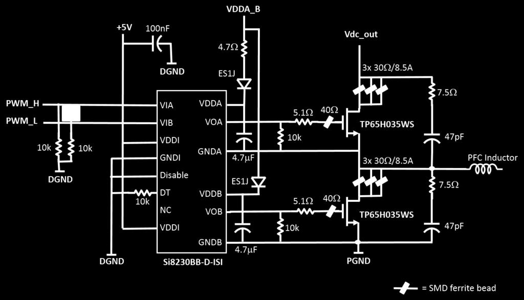
4 Block Diagram AC Line In L N Filter Input Current + Voltage sense PFC Inductor Synchronous Bridge + Vdc out - PE PWM Digital Control - DSP - Firmware Vout Sense Auxiliary DC/DC Converter


 Negative Half")
5 The Bridgless Totempole PFC Topology Simplified schematic, CCM operation S2 on S1 on S2 off S1 off Positive Half Cycle (Vac>0) Negative Half Cycle (Vac<0)
6 6 GaN Synchronous Half Bridge


7 GaN Cascode Power Switches 3 rd Generation GaN cascode technology. Normally-off 30V Si FET in series with normally-on 650V GaN FET Robust Si gate; standard gate drive; Vth=3.9V Also available: Ron=50, 72, mω SMD packaging
8 GaN Cascode Power Switches Qoss is the dominate component of Qrr
9 AEC-Q101 Qualified GaN Tests and Test Conditions Test Symbol Conditions Sample Pass Criteria TPH3205WSQA: First device with automotive qualification, in-stock and available. Additional devices are now in the qualification process. High Temperature Reverse Bias Highly Accelerated Temp and Humidity Temperature Cycle Temperature Cycling Hot Test HTRB HAST TC TCHT T J =150 C, V DS =650V, 1000 HRS 130 C, 85% RH, 33.3 PSI, Bias=100V, 96 HRS -55 C / 150 C, 2 Cycles / HR, 1000 Cycles 125 C Test After TC Wire Bond Integrity WBI 150 C, 500 HRS 3 lots, 77 parts per lot, 231 total parts 3 lots, 5 parts per lot, 15 total parts 0 Fails PASS 0 Fails PASS 0 Fails PASS 0 Fails PASS 0 Fails PASS Test Specifications Power Cycle PC 25 C / 125 C, T=105 C, 15,000 Cycles 0 Fails PASS Idss Igss Parameter Spec Limit Max Shift Allowed <40µA <100nA Dynamic R(on) 62mΩ <20% Vth 2.6/1.6 V <20% 5x increase (10x increase for environmental testing) Not applicable (low leakage) High Temperature Storage Life High Temperature Gate Bias (Cascode) High Temperature Gate Bias (HEMT only) High Humidity High Temp Reverse Bias Unbiased Accelerated Stress Test HTSL 150 C, 1000 HRS HTGB 150 C, 1000 HRS, V GSS =18V HTGB #2 H3TRB UHAST 150 C, 1000 HRS, V GSS =-35V 85 C/85% RH, 1000 HRS, 100V 130 C, 85% RH, 96 HRS 3 lots, 77 parts per lot, 231 total parts 0 Fails PASS 0 Fails PASS 0 Fails PASS 0 Fails PASS 0 Fails PASS Destructive Physical Analysis DPA Post TC & HAST 3 lots, 2 parts per lot, 6 total parts 0 Fails PASS


10 Effects of Off State Acceleration Factors Process variability is as important as determining acceleration factors Use plot with extrapolated lifetime for all devices tested ~300 devices from 9 different lots Test conditions ranged: VD from 1150V to 1300V Temperature from -20 C to 150 C Process evaluated at 480V Temperature range for automotive is -40 C to 150 C Nominal temperature expected to be 85 C Process shows 1% failure years Off state for -40 C 480V -40 C 85 C 150 C Process shows excellent extrapolated lifetime with good stability

11 GaN Half-Bridge Design Details
. http://www.transphormusa.")
12 GaN Half Bridge Design Details Ferrite bead in series with Drain: Damps ringing, overshoot increases. Overshoot is well within the specified transient-voltage limit (800V).
13 13 PFC Inductor Design
14 PFC inductor design Two versions of the inductor have been developed, - For use at different switching frequencies - Wound on the same toroidal core Frequency L (typical) Turns AWG Core R (T=25C) 45 khz 577 µh CH High Flux Ω 100 khz 338 µh CH High Flux Ω 45 khz 100 khz


15 PFC inductor design High Flux core permits operation at max current with a single core. Alternatives: - MPP or Sendust would require larger or stacked cores of the same size - Ferrite E core would be larger 15A 2 56Turns = 1188Ampere Turns
16 16 AC Power Entry: EMI Filter


17 EMI Filter 8121-RC 8121-RC PFC Inductor

18 EMI Filter This plot shows Z from the switching inductor node looking back into the AC line, neglecting the LISN terminating impedance. Test result from the TTP4000W066 4kW PFC evaluation board which uses the same EMI filer.
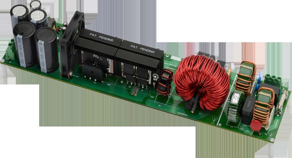

19 19 PCB
 Outer Layers: 2oz (70µm) b) Inner Layers: 1oz")

20 PCB 388mm Fabrication Notes: 4 Layers 92mm Board Thickness: 93 mils Copper Thickness: a) Outer Layers: 2oz (70µm) b) Inner Layers: 1oz (35µm) Material: a) Base material: FR4 140 Tg as per IPC-4101 b) Prepreg material: FR4 as per IPC-4101 Minimum track thickness: 6 mil Minimum spacing: 6 mil


21 PCB Vdc out Top Layer Agnd Dgnd Pgnd Mid Layer 2 +3V3 Vdc out Mid Layer 1 Pgnd Bottom Layer
22 22 Control: Algorithm, Firmware Implementation

23 Digital Signal Controller TMS320F28335PGFA Texas Instruments Digital Signal Controller (DSC). QFP package was used to accommodate small production runs. BGA is significantly smaller. Use of a vertical, fixed (soldered/no-connector) daughter board for the DSP would improve power density.
24 Control Diagram for the Totempole PFC 24
25 25 Test Results
26 Efficiency vs Load 99% Load Efficiency 50kHz 99% Load Efficiency 100kHz 98% 98% 97% 97% 96% Efficiency (%) 96% 95% 90 VAC 115 VAC 180 VAC 230 VAC 260 VAC Efficiency (%) 95% 94% 93% 92% 90 VAC 115 VAC 180 VAC 230 VAC 94% 91% 260 VAC 93% Input Power (W) [15Arms rated] 90% Input Power (W) [15Arms rated]
27 Power Factor vs Load 1 POWER FACTOR versus Input Power, 50kHz 1 POWER FACTOR versus Input Power, 100kHz 0,98 Power Factor 0,96 0,94 90VAC 115 VAC 180 VAC 230 VAC 260 VAC Power Factor 0,98 0,96 90VAC 115 VAC 180 VAC 230 VAC 260 VAC 0,92 0, Input Power (W) 0, Input Power (W)


28 Current and Voltage Waveforms 90 VAC, 50% Load. 90 VAC, 100% Load. Red: Vin, 100V/div Gold: Iin, 5A/div 5ms/div Red: Vin, 100V/div Gold: Iin, 10A/div 5ms/div 230 VAC, 50% Load. 230 VAC, 100% Load. Red: Vin, 200V/div Gold: Iin, 5A/div 5ms/div Red: Vin, 200V/div Gold: Iin, 10A/div 5ms/div


29 Start up Operation 90 VAC, 0% Load. Red: VIN, 100 V / div. Gold: IIN, 5 A / div. Green: Vout, 100 V / div., 200 ms / div. 90 VAC, 100% Load. Red: VIN, 100 V / div. Gold: IIN, 10 A / div. Green: Vout, 100 V / div., 200 ms / div.
30 Danke fürs Zuhören
VDSS (V) 650 V(TR)DSS (V) 800. RDS(on)eff (mω) max* 85. QRR (nc) typ 90. QG (nc) typ 10
 650 V(TR)DSS (V) 800. RDS(on)eff (mω) max* 85. QRR (nc) typ 90. QG (nc) typ 10") TP65H070L Series 650V GaN FET PQFN Series Preliminary Description The TP65H070L 650V, 72mΩ Gallium Nitride (GaN) FET are normally-off devices. It combines state-of-the-art high voltage GaN HEMT and low
TP65H070L Series 650V GaN FET PQFN Series Preliminary Description The TP65H070L 650V, 72mΩ Gallium Nitride (GaN) FET are normally-off devices. It combines state-of-the-art high voltage GaN HEMT and low
VDSS (V) 650 V(TR)DSS (V) 800 RDS(on)eff (mω) max* 180. QRR (nc) typ 47. QG (nc) typ 10
 650 V(TR)DSS (V) 800 RDS(on)eff (mω) max* 180. QRR (nc) typ 47. QG (nc) typ 10") TP65H150LSG 650V GaN FET PQFN Series Preliminary Datasheet Description The TP65H150LSG 650V, 150mΩ Gallium Nitride (GaN) FET are normally-off devices. They combine state-of-the-art high voltage GaN HEMT
TP65H150LSG 650V GaN FET PQFN Series Preliminary Datasheet Description The TP65H150LSG 650V, 150mΩ Gallium Nitride (GaN) FET are normally-off devices. They combine state-of-the-art high voltage GaN HEMT
Reference Design. TDTTP3300-RD 3.3kW Bridgeless Totem-pole PFC. Test Report
 Reference Design TDTTP3300-RD 3.3kW Bridgeless Totem-pole PFC Table of Contents 1 Introduction... 4 1.1 Design resources... 4 2 Power supply specifications... 5 3 3-D board image... 6 4 Performance data...
VDSS (V) 650. V(TR)DSS (V) 800 RDS(on)eff (mω) max* 180. QRR (nc) typ 52. QG (nc) typ 6.2
 650. V(TR)DSS (V) 800 RDS(on)eff (mω) max* 180. QRR (nc) typ 52. QG (nc) typ 6.2") 650V GaN FET PQFN Series Not recommended for new designs Description The TPH3206L Series 650V, 150mΩ Gallium Nitride (GaN) FETs are normally-off devices. They combine state-of-the-art high voltage GaN
650V GaN FET PQFN Series Not recommended for new designs Description The TPH3206L Series 650V, 150mΩ Gallium Nitride (GaN) FETs are normally-off devices. They combine state-of-the-art high voltage GaN
VDSS (V) 650 V(TR)DSS (V) 800. RDS(on)eff (mω) max* 130. QRR (nc) typ 54. QG (nc) typ 10
 650 V(TR)DSS (V) 800. RDS(on)eff (mω) max* 130. QRR (nc) typ 54. QG (nc) typ 10") 650V GaN FET PQFN Series Not recommended for new designs Description The TPH3208L Series 650V, 110mΩ Gallium Nitride (GaN) FETs are normally-off devices. They combine state-of-the-art high voltage GaN
650V GaN FET PQFN Series Not recommended for new designs Description The TPH3208L Series 650V, 110mΩ Gallium Nitride (GaN) FETs are normally-off devices. They combine state-of-the-art high voltage GaN
VDSS (V) 900. V(TR)DSS (V) 1000 RDS(on)eff (mω) max* 205. QRR (nc) typ 49. QG (nc) typ 10
 900. V(TR)DSS (V) 1000 RDS(on)eff (mω) max* 205. QRR (nc) typ 49. QG (nc) typ 10") 900V GaN FET in TO-220 (source tab) Description The TP90H180PS 900V, 170mΩ Gallium Nitride (GaN) FET is a normally-off device. It combines state-of-the-art high voltage GaN HEMT and low voltage silicon
900V GaN FET in TO-220 (source tab) Description The TP90H180PS 900V, 170mΩ Gallium Nitride (GaN) FET is a normally-off device. It combines state-of-the-art high voltage GaN HEMT and low voltage silicon
VDSS (V) 650 V(TR)DSS (V) 800 RDS(on)eff (mω) max* 180. QRR (nc) typ 52. QG (nc) typ 6.2 VIN=230VAC; VOUT=390VDC VIN=380VDC; VOUT=240VAC
 650 V(TR)DSS (V) 800 RDS(on)eff (mω) max* 180. QRR (nc) typ 52. QG (nc) typ 6.2 VIN=230VAC; VOUT=390VDC VIN=380VDC; VOUT=240VAC") 650V GaN FET in TO-220 (source tab) Description The TPH3206PSB 650V, 150mΩ Gallium Nitride (GaN) FET is a normally-off device. It combines state-of-the-art high voltage GaN HEMT and low voltage silicon
650V GaN FET in TO-220 (source tab) Description The TPH3206PSB 650V, 150mΩ Gallium Nitride (GaN) FET is a normally-off device. It combines state-of-the-art high voltage GaN HEMT and low voltage silicon
VDSS (V) 650 V(TR)DSS (V) 800 RDS(on)eff (mω) max* 60. QRR (nc) typ 136. QG (nc) typ 28 VIN=230VAC; VOUT=390VDC VIN=380VDC; VOUT=240VAC
 650 V(TR)DSS (V) 800 RDS(on)eff (mω) max* 60. QRR (nc) typ 136. QG (nc) typ 28 VIN=230VAC; VOUT=390VDC VIN=380VDC; VOUT=240VAC") 650V GaN FET in TO-247 (source tab) Description The TPH3205WSB 650V, 49mΩ Gallium Nitride (GaN) FET is a normally-off device. It combines state-of-the-art high voltage GaN HEMT and low voltage silicon
650V GaN FET in TO-247 (source tab) Description The TPH3205WSB 650V, 49mΩ Gallium Nitride (GaN) FET is a normally-off device. It combines state-of-the-art high voltage GaN HEMT and low voltage silicon
VDSS (V) 650 V(TR)DSS (V) 800 RDS(on)eff (mω) max* 130. QRR (nc) typ 54. QG (nc) typ 14 VIN=230VAC; VOUT=390VDC VIN=380VDC; VOUT=240VAC
 650 V(TR)DSS (V) 800 RDS(on)eff (mω) max* 130. QRR (nc) typ 54. QG (nc) typ 14 VIN=230VAC; VOUT=390VDC VIN=380VDC; VOUT=240VAC") 650V GaN FET TO-220 Series Description The TPH3208PS 650V, 110mΩ Gallium Nitride (GaN) FET is a normally-off device. It combines state-of-the-art high voltage GaN HEMT and low voltage silicon MOSFET technologies
650V GaN FET TO-220 Series Description The TPH3208PS 650V, 110mΩ Gallium Nitride (GaN) FET is a normally-off device. It combines state-of-the-art high voltage GaN HEMT and low voltage silicon MOSFET technologies
PRELIMINARY. VDSS (V) 600 V(TR)DSS (V) 750 RDS(on)eff (mω) max* 60. QRR (nc) typ 120. QG (nc) typ 22 PRELIMINARY
 600 V(TR)DSS (V) 750 RDS(on)eff (mω) max* 60. QRR (nc) typ 120. QG (nc) typ 22 PRELIMINARY") PRELIMINARY TPH3205ESBET 600V GaN FET in TO-268 (source tab) Description The TPH3205ESBET 600V, 49mΩ Gallium Nitride (GaN) FET is a normally-off device. It combines state-of-the-art high voltage GaN HEMT
PRELIMINARY TPH3205ESBET 600V GaN FET in TO-268 (source tab) Description The TPH3205ESBET 600V, 49mΩ Gallium Nitride (GaN) FET is a normally-off device. It combines state-of-the-art high voltage GaN HEMT
Reference Design. TDTTP3300-RD 3.3kW Bridgeless Totem-pole PFC. Test Report
 Reference Design TDTTP3300-RD 3.3kW Bridgeless Totem-pole PFC Table of Contents 1 Introduction... 4 1.1 Design resources... 4 2 Power supply specifications... 5 3 3-D board image... 6 4 Performance data...
VDS (V) min 650 VTDS (V) max 800 RDS(on) (mω) max* 130. Qrr (nc) typ 54. * Dynamic R(on)
 min 650 VTDS (V) max 800 RDS(on) (mω) max* 130. Qrr (nc) typ 54. * Dynamic R(on)") 650V Cascode GaN FET in TO-220 (source tab) Description The TPH3208PS 650V, 110mΩ gallium nitride (GaN) FET is a normally-off device. Transphorm GaN FETs offer better efficiency through lower gate charge,
650V Cascode GaN FET in TO-220 (source tab) Description The TPH3208PS 650V, 110mΩ gallium nitride (GaN) FET is a normally-off device. Transphorm GaN FETs offer better efficiency through lower gate charge,
Designing a 99% Efficient Totem Pole PFC with GaN. Serkan Dusmez, Systems and applications engineer
 Designing a 99% Efficient Totem Pole PFC with GaN Serkan Dusmez, Systems and applications engineer 1 What will I get out of this session? Purpose: Why GaN Based Totem-pole PFC? Design guidelines for getting
IBM Technology Symposium
 IBM Technology Symposium Impact of Input Voltage on Server PSU- Efficiency, Power Density and Cost Design. Build. Ship. Service. Sriram Chandrasekaran November 13, 2012 Presentation Outline Redundant Server
TPH3205WSB. 650V Cascode GaN FET in TO-247 (source tab)
") 650V Cascode GaN FET in TO-247 (source tab) Description The TPH3205WSB 650V, 52mΩ gallium nitride (GaN) FET is a normally-off device. Transphorm GaN FETs offer better efficiency through lower gate charge,
650V Cascode GaN FET in TO-247 (source tab) Description The TPH3205WSB 650V, 52mΩ gallium nitride (GaN) FET is a normally-off device. Transphorm GaN FETs offer better efficiency through lower gate charge,
VDS (V) min 600 VTDS (V) max 750 RDS(on) (mω) max* 63. Qrr (nc) typ 136. * Dynamic R(on)
 min 600 VTDS (V) max 750 RDS(on) (mω) max* 63. Qrr (nc) typ 136. * Dynamic R(on)") 600V Cascode GaN FET in TO-247 (source tab) Not recommended for new designs see TP65H050WS Description The TPH3205WS 600V, 52mΩ gallium nitride (GaN) FET is a normally-off device. Transphorm GaN FETs offer
600V Cascode GaN FET in TO-247 (source tab) Not recommended for new designs see TP65H050WS Description The TPH3205WS 600V, 52mΩ gallium nitride (GaN) FET is a normally-off device. Transphorm GaN FETs offer
VDS (V) min 650 VTDS (V) max 800 RDS(on) (mω) max* 60. Qrr (nc) typ 136. Qg (nc) typ 28. * Dynamic RDS(on)
 min 650 VTDS (V) max 800 RDS(on) (mω) max* 60. Qrr (nc) typ 136. Qg (nc) typ 28. * Dynamic RDS(on)") 650V Cascode GaN FET in TO-247 (source tab) Description The TPH3205WSB 650V, 49mΩ gallium nitride (GaN) FET is a normally-off device. Transphorm GaN FETs offer better efficiency through lower gate charge,
650V Cascode GaN FET in TO-247 (source tab) Description The TPH3205WSB 650V, 49mΩ gallium nitride (GaN) FET is a normally-off device. Transphorm GaN FETs offer better efficiency through lower gate charge,
VDS (V) min 600 VTDS (V) max 750 RDS(on) (mω) max* 180. Qrr (nc) typ 54. * Dynamic R(on)
 min 600 VTDS (V) max 750 RDS(on) (mω) max* 180. Qrr (nc) typ 54. * Dynamic R(on)") 600V Cascode GaN FET in TO-220 (drain tab) Description The 600V, 150mΩ gallium nitride (GaN) FET is a normally-off device. Transphorm GaN FETs offer better efficiency through lower gate charge, faster
600V Cascode GaN FET in TO-220 (drain tab) Description The 600V, 150mΩ gallium nitride (GaN) FET is a normally-off device. Transphorm GaN FETs offer better efficiency through lower gate charge, faster
TPH3212PS. 650V Cascode GaN FET in TO-220 (source tab)
") 650V Cascode GaN FET in TO-220 (source tab) Description The TPH3212PS 650V, 72mΩ gallium nitride (GaN) FET is a normally-off device. Transphorm GaN FETs offer better efficiency through lower gate charge,
650V Cascode GaN FET in TO-220 (source tab) Description The TPH3212PS 650V, 72mΩ gallium nitride (GaN) FET is a normally-off device. Transphorm GaN FETs offer better efficiency through lower gate charge,
Power of GaN. Enabling designers to create smaller, more efficient and higher-performing AC/DC power supplies
 Power of GaN Enabling designers to create smaller, more efficient and higher-performing AC/DC power supplies Steve Tom Product Line Manager, GaN Products stom@ti.com Solving power and energy-management
Application Note 0011
 0011 PQFN GaN FETs Paralleling PCB 1. Introduction Trasphorm s PQFN (Power Quad Flatpack No Lead) package incorporates a DPC (Direct Plated Cu) substrate and a Cu lead frame encapsulated in a green molding
GaN Based Power Conversion: Moving On! Tim McDonald APEC Key Component Technologies for Power Electronics in Electric Drive Vehicles
 1 GaN Based Power Conversion: Moving On! Key Component Technologies for Power Electronics in Electric Drive Vehicles Tim McDonald APEC 2013 2 Acknowledgements Collaborators: Tim McDonald (1), Han S. Lee
GaN in Practical Applications
 in Practical Applications 1 CCM Totem Pole PFC 2 PFC: applications and topology Typical AC/DC PSU 85-265 V AC 400V DC for industrial, medical, PFC LLC 12, 24, 48V DC telecomm and server applications. PFC
Design Guide. 100 khz Dual Active Bridge for 3.3kW Bi-directional Battery Charger. Introduction. Converter Design
 100 khz Dual Active Bridge for 3.3kW Bidirectional Battery Charger Introduction Dual Active Bridge (DAB) is a classic topology for bidirectional power conversion requiring a wide range of voltage transfer
Title. Description. Date 16 th August, Revision 1.1 RD W Telecoms DC/DC PSU Input : 37Vdc to 60Vdc Output : 32V/10A
 Title Description RD008 320W Telecoms DC/DC PSU Input : 37Vdc to 60Vdc Output : 32V/10A Date 16 th August, 2007 Revision 1.1 WWW.ConverterTechnology.CO.UK RD008 320W Push-Pull Converter August 16, 2007
GaN Reliability Through Integration and Application Relevant Stress Testing
 GaN Reliability Through Integration and Application Relevant Stress Testing APEC 2018 PSMA Sponsored Industry Session: Reliability and Ruggedness How to Address these Challenges in Wide Bandgap Semiconductor
High-Voltage (600 V) GaN Power Devices: Status and Benefits Power Electronics Conference 2017 Munich Airport Hilton, December 05, 2017
 GaN Power Devices: Status and Benefits Power Electronics Conference 2017 Munich Airport Hilton, December 05, 2017") High-Voltage (600 V) GaN Power Devices: Status and Benefits Power Electronics Conference 2017 Munich Airport Hilton, December 05, 2017 Th. Detzel, O. Häberlen, A. Bricconi, A. Charles, G. Deboy, T. McDonald
High-Voltage (600 V) GaN Power Devices: Status and Benefits Power Electronics Conference 2017 Munich Airport Hilton, December 05, 2017 Th. Detzel, O. Häberlen, A. Bricconi, A. Charles, G. Deboy, T. McDonald
Designing High density Power Solutions with GaN Created by: Masoud Beheshti Presented by: Xaver Arbinger
 Designing High density Power Solutions with GaN Created by: Masoud Beheshti Presented by: Xaver Arbinger Topics Why GaN? Integration for Higher System Performance Application Examples Taking GaN beyond
Designing Reliable and High-Density Power Solutions with GaN
 Designing Reliable and High-Density Power Solutions with GaN 1 Detailed agenda Why is GaN Exciting GaN Fundamentals Cost and Reliability Totem Pole PFC Isolated LLC Motor Drive LiDAR Driving GaN Choosing
Designing reliable and high density power solutions with GaN. Created by: Masoud Beheshti Presented by: Paul L Brohlin
 Designing reliable and high density power solutions with GaN Created by: Masoud Beheshti Presented by: Paul L Brohlin What will I get out of this presentation? Why GaN? Integration for System Performance
Symbol Parameter Typical
 PRODUCT SUMMARY (TYPICAL) V DS (V) 650 R DS(on) (m ) 110 Q rr (nc) 54 Features Low Q rr Free-wheeling diode not required Low-side Quiet Tab for reduced EMI RoHS compliant High frequency operation Applications
Get Your GaN PhD in Less Than 60 Minutes!
 Get Your GaN PhD in Less Than 60 Minutes! 1 Detailed agenda Why is GaN Exciting GaN Fundamentals Cost and Reliability Totem Pole PFC Isolated LLC Motor Drive LiDAR Driving GaN Choosing a GaN Tools 4 Why
Impact of Fringing Effects on the Design of DC-DC Converters
 Impact of Fringing Effects on the Design of DC-DC Converters Michael Seeman, Ph.D. Founder / CEO. 2018 APEC PSMA/PELS 2018. Outline Fringe-field loss: What does a power supply designer need to know? Which
State of Demonstrated HV GaN Reliability and Further Requirements
 State of Demonstrated HV GaN Reliability and Further Requirements APEC 2015 Charlotte, NC Tim McDonald Steffen Sack, Deepak Veereddy, Yang Pan, Hyeongnam Kim, Hari Kannan, Mohamed Imam Agenda What Composes
The Quest for High Power Density
 The Quest for High Power Density Welcome to the GaN Era Power Conversion Technology Drivers Key design objectives across all applications: High power density High efficiency High reliability Low cost 2
Breaking Speed Limits with GaN Power ICs March 21 st 2016 Dan Kinzer, COO/CTO
 Breaking Speed Limits with GaN Power ICs March 21 st 2016 Dan Kinzer, COO/CTO dan.kinzer@navitassemi.com 1 Efficiency The Need for Speed Tomorrow? Today 100kHz 1MHz 10MHz Bulky, Heavy Small, Light & Expensive
Demands for High-efficiency Magnetics in GaN Power Electronics
 APEC 2014, Fort Worth, Texas, March 16-20, 2014, IS2.5.3 Demands for High-efficiency Magnetics in GaN Power Electronics Yifeng Wu, Transphorm Inc. Table of Contents 1. 1 st generation 600V GaN-on-Si HEMT
AONS V N-Channel MOSFET
 AONS3634 3V N-Channel MOSFET General Description Trench Power MOSFET technology Low R DS(ON) Low Gate Charge High Current Capability RoHS and Halogen-Free Compliant Product Summary V DS I D (at V GS =V)
Vishay Siliconix AN724 Designing A High-Frequency, Self-Resonant Reset Forward DC/DC For Telecom Using Si9118/9 PWM/PSM Controller.
 AN724 Designing A High-Frequency, Self-Resonant Reset Forward DC/DC For Telecom Using Si9118/9 PWM/PSM Controller by Thong Huynh FEATURES Fixed Telecom Input Voltage Range: 30 V to 80 V 5-V Output Voltage,
Application Note 0009
 Recommended External Circuitry for Transphorm GaN FETs Application Note 9 Table of Contents Part I: Introduction... 2 Part II: Solutions to Suppress Oscillation... 2 Part III: The di/dt Limits of GaN Switching
GaN Power ICs at 1 MHz+: Topologies, Technologies and Performance
 GaN Power ICs at 1 MHz+: Topologies, Technologies and Performance PSMA Industry Session, Semiconductors Dan Kinzer, CTO/COO dan.kinzer@navitassemi.com March 2017 Power Electronics: Speed & Efficiency are
Interleaved PFC technology bring up low ripple and high efficiency
 Interleaved PFC technology bring up low ripple and high efficiency Tony Huang 黄福恩 Texas Instrument Sept 12,2007 1 Presentation Outline Introduction to Interleaved transition mode PFC Comparison to single-channel
MAXREFDES121# Isolated 24V to 3.3V 33W Power Supply
 System Board 6309 MAXREFDES121# Isolated 24V to 3.3V 33W Power Supply Maxim s power-supply experts have designed and built a series of isolated, industrial power-supply reference designs. Each of these
EVALUATION KIT AVAILABLE 28V, PWM, Step-Up DC-DC Converter PART V IN 3V TO 28V
 19-1462; Rev ; 6/99 EVALUATION KIT AVAILABLE 28V, PWM, Step-Up DC-DC Converter General Description The CMOS, PWM, step-up DC-DC converter generates output voltages up to 28V and accepts inputs from +3V
Application Note 0006
 VGS Transient Tolerance of Transphorm GaN FETs Abstract This document provides a guideline for allowable transient voltages between gate and source pins. Table of Contents Abstract... 1 Introduction...
Improving Totem-Pole PFC and On Board Charger performance with next generation components
 Improving Totem-Pole PFC and On Board Charger performance with next generation components Anup Bhalla 1) 1) United Silicon Carbide, Inc., 7 Deer Park Drive, Monmouth Jn., NJ USA E-mail: abhalla@unitedsic.com
Recommended External Circuitry for Transphorm GaN FETs. Zan Huang Jason Cuadra
 Recommended External Circuitry for Transphorm GaN FETs Zan Huang Jason Cuadra Application Note Rev. 1.0 November 22, 2016 Table of Contents 1 Introduction 3 2 Sustained oscillation 3 3 Solutions to suppress
A new era in power electronics with Infineon s CoolGaN
 A new era in power electronics with Infineon s CoolGaN Dr. Gerald Deboy Senior Principal Power Discretes and System Engineering Power management and multimarket division Infineon will complement each of
Making Reliable and High-Density GaN Solutions a Reality
 Making Reliable and High-Density GaN Solutions a Reality December 5, 2017 Franz Xaver Arbinger Masoud Beheshti 1 Today s Topics Why is GaN Exciting GaN Fundamentals Cost and Reliability Totem Pole PFC
Bias Stress Testing of SiC MOSFETs
 Bias Stress Testing of SiC MOSFETs Robert Shaw Manager, Test and Qualification August 15 th, 2014 Special thanks to the U.S. Department of Energy for funding this under SBIR DE-SC0011315. Outline Objectives
X-GaN TTP Simulation Manual Ver. 1.0
 Panasonic web simulation for Totem Pole PFC (TTP) featuring: 1. PGA26E07BA 600V 70mΩ / PGA26E19BA 600V 190mΩ X-GaN Power Transistor 2. AN34092B Single channel X-GaN Gate Driver IC 3. Web-based simulator
GS66502B Bottom-side cooled 650 V E-mode GaN transistor Preliminary Datasheet
 GS66502B Features 650 V enhancement mode power switch Bottom-side cooled configuration R DS(on) = 200 mω I DS(max) = 7.5 A Ultra-low FOM Island Technology die Low inductance GaNPX package Easy gate drive
Unlocking the Power of GaN PSMA Semiconductor Committee Industry Session
 Unlocking the Power of GaN PSMA Semiconductor Committee Industry Session March 24 th 2016 Dan Kinzer, COO/CTO dan.kinzer@navitassemi.com 1 Mobility (cm 2 /Vs) EBR Field (MV/cm) GaN vs. Si WBG GaN material
INTRODUCTION THEORY. Formulas:
 May 2011 Rev. 1.0.0 INTRODUCTION The XRP77XX series family integrates Internal Gate Drivers for all 4 PWM channels. These drivers are optimized to drive both high-side and low side N-MOSFETs for synchronous
+ - GaN. Output Voltage. Auxiliary Supply: Input High Voltage. Application Note: TDPS500E2C1Totem Pole PFC Evaluation Board GND. 1.
 L N Auxiliary Supply: Application Note: TDPS500E2C1 TDPS500E2C1Totem Pole PFC Evaluation Board 1. Introduction The Evaluation Board for a bridgeless totem-pole Power-Factor-Correction (PFC) circuit, using
235 W Maximum Power Dissipation (whole module) 470 T J Junction Operating Temperature -40 to 150. Torque strength
 470 T J Junction Operating Temperature -40 to 150. Torque strength") Discontinued PRODUCT SUMMARY (TYPICAL) V DS (V) 600 R DS(on) (m ) 30 GaN Power Hybrid HEMT Half-Bridge Module Features High frequency operation Free-wheeling diode not required Applications Compact DC-DC
Discontinued PRODUCT SUMMARY (TYPICAL) V DS (V) 600 R DS(on) (m ) 30 GaN Power Hybrid HEMT Half-Bridge Module Features High frequency operation Free-wheeling diode not required Applications Compact DC-DC
GS66504B Bottom-side cooled 650 V E-mode GaN transistor Preliminary Datasheet
 Features 650 V enhancement mode power switch Bottom-side cooled configuration R DS(on) = 100 mω I DS(max) = 15 A Ultra-low FOM Island Technology die Low inductance GaNPX package Easy gate drive requirements
Symbol Parameter Typical
 PRODUCT SUMMARY (TYPICAL) V DS (V) 600 R DS(on) ( ) 0.29 Q rr (nc) 29 Features Low Q rr Free-wheeling diode not required Low-side Quiet Tab for reduced EMI RoHS compliant High frequency operation Applications
GS66508P Bottom-side cooled 650 V E-mode GaN transistor Preliminary Datasheet
 Features 650 V enhancement mode power switch Bottom-side cooled configuration R DS(on) = 50 mω I DS(max) = 30 A Ultra-low FOM Island Technology die Low inductance GaNPX package Easy gate drive requirements
ANP030. Contents. Application Note AP2014/A Synchronous PWM Controller. 1. AP2014/A Specification. 2. Hardware. 3. Design Procedure. 4.
 Contents 1. AP2014/A Specification 1.1 Features 1.2 General Description 1.3 Pin Assignments 1.4 Pin Descriptions 1.5 Block Diagram 1.6 Absolute Maximum Ratings 2. Hardware 2.1 Introduction 2.2 Description
High voltage GaN cascode switches shift power supply design trends. Eric Persson Executive Director, GaN Applications and Marketing
 High voltage GaN cascode switches shift power supply design trends Eric Persson Executive Director, GaN Applications and Marketing September 4, 2014 1 Outline for Today s PSMA PTR Presentation Why do we
GS66508B Bottom-side cooled 650 V E-mode GaN transistor Preliminary Datasheet
 Features 650 V enhancement mode power switch Bottom-side cooled configuration R DS(on) = 50 mω I DS(max) = 30 A Ultra-low FOM Island Technology die Low inductance GaNPX package Easy gate drive requirements
25 Watt DC/DC converter using integrated Planar Magnetics
 technical note 25 Watt DC/DC converter using integrated Planar Magnetics Philips Components 25 Watt DC/DC converter using integrated Planar Magnetics Contents Introduction 2 Converter description 3 Converter
AN2001 Application note
 Application note VIPower : the VIPer53-E single output reference board with 90 to 264 Vac input, 24 W output Introduction The VIPer53-E combines an enhanced current mode PWM controller with a high voltage
GS66516B Bottom-side cooled 650 V E-mode GaN transistor Preliminary Datasheet
 Features 650 V enhancement mode power switch Bottom-side cooled configuration R DS(on) = 25 mω I DS(max) = 60 A Ultra-low FOM Island Technology die Low inductance GaNPX package Easy gate drive requirements
GaN Power ICs: Integration Drives Performance
 GaN Power ICs: Integration Drives Performance Stephen Oliver, VP Sales & Marketing stephen.oliver@navitassemi.com Bodo s Power Conference, Munich December 5 th, 2017 Navitas Semiconductor Inc. World s
Cree PV Inverter Tops 1kW/kg with All-SiC Design
 Cree PV Inverter Tops 1kW/kg with All-SiC Design Alejandro Esquivel September, 2014 Power Forum 2014 (Bologna) presentation sponsored by: Presentation Outline 1. Meeting an Industry Need a) 1kW/Kg b) No
ATR28XXS SERIES HYBRID - HIGH RELIABILITY DC-DC CONVERTER. 28V Input, Single Output. Description ATR. Features.
 PD-94549C HYBRID - HIGH RELIABILITY DC-DC CONVERTER ATR28XXS SERIES 28V Input, Single Output Description The ATR28XXS Series of DC-DC converters feature high power density and an extended temperature range
MOSFET. CoolMOS C6. Data Sheet. Industrial & Multimarket. Metal Oxide Semiconductor Field Effect Transistor
 MOSFET Metal Oxide Semiconductor Field Effect Transistor CoolMOS C6 600V CoolMOS C6 Power Transistor Data Sheet Rev. 2.0, 2009-09-25 Final Industrial & Multimarket IPA60R125C6, IPB60R125C6 IPP60R125C6
Single Switch Forward Converter
 Single Switch Forward Converter This application note discusses the capabilities of PSpice A/D using an example of 48V/300W, 150 KHz offline forward converter voltage regulator module (VRM), design and
EPC2107 Enhancement-Mode GaN Power Transistor Half-Bridge with Integrated Synchronous Bootstrap
 EPC7 Enhancement-Mode GaN Power Transistor Half-Bridge with Integrated Synchronous Bootstrap V DSS, V R DS(on), 9 m I D,.7 A EFFICIENT POWER CONVERSION HAL EPC7 Gallium Nitride is grown on Silicon Wafers
WD1015 WD1015. Descriptions. Features. Order information. Applications. Http//: 1.5MHz, 1.2A, Step-down DC-DC Converter
 1.5MHz, 1.2A, Step-down DC-DC Converter Http//:www.sh-willsemi.com Descriptions The is a high efficiency, synchronous step down DC-DC converter optimized for battery powered portable applications. It supports
MW75S single-output AC/DC power supply Power factor corrected Vin, 2 28Vout, 75 watts. I - M3 inserts. Max
 MW7S single-output AC/DC power supply Power factor corrected 9 26Vin, 2 28Vout, 7 watts HOW TO ORDER MW 7 - S M / 28 - I Series Total Output Power(W) Single Output Unscreened (I) or Screened(M) INPUT CHARACTERISTICS
GaN Reliability Report 2018
 GaN Reliability Report 2018 GaN-on-Silicon Reliability and Qualification Report A summary analysis of application-specific stress testing methodologies and results demonstrating the reliability of Gallium
The First Step to Success Selecting the Optimal Topology Brian King
 The First Step to Success Selecting the Optimal Topology Brian King 1 What will I get out of this session? Purpose: Inside the Box: General Characteristics of Common Topologies Outside the Box: Unique
1.2 KW, N+1 REDUNDANT, POWER-FACTOR CORRECTED, 12V FRONT END
 PS2379 CHARACTERIZATION 1.2 KW, N+1 REDUNDANT, POWER-FACTOR CORRECTED, 12V FRONT END October 26, 2005 Rev 1 Table of Contents 0. Introduction 4-16 1. Line Current Harmonics 17-18 2. Line Conducted EMI
800 W PFC evaluation board
 800 W PFC evaluation board EVAL_800W_PFC_C7_V2 / SP001647120 / SA001647124 High power density 800 W 130 khz platinum server design with analog & digital control Garcia Rafael (IFAT PMM ACDC AE) Zechner
ABC400 Series is a compact and efficient series of AC-DC open frame power supplies suited for telecom, datacom and many other applications.
 is a compact and efficient series of AC-DC open frame power supplies suited for telecom, datacom and many other applications. The family meets the international information technology safety standards
MP A, 55V, 100kHz Step-Down Converter with Programmable Output OVP Threshold
 The Future of Analog IC Technology MP24943 3A, 55V, 100kHz Step-Down Converter with Programmable Output OVP Threshold DESCRIPTION The MP24943 is a monolithic, step-down, switch-mode converter. It supplies
GS66516B Bottom-side cooled 650 V E-mode GaN transistor Preliminary Datasheet
 Features 650 V enhancement mode power switch Bottom-side cooled configuration R DS(on) = 25 mω I DS(max) = 60 A Ultra-low FOM Island Technology die Low inductance GaNPX package Easy gate drive requirements
SPS10-24 Series small size isolated DC/DC converters
 SPS10-24 Series small size isolated DC/DC converters Features High Efficiency Wide operating temperature range ( -40 C to +85 C ) Wide 2:1 input range Dimensions 35.60 x 8.50 x 26.0 (mm) Built in over
MAXREFDES116# ISOLATED 24V TO 5V 40W POWER SUPPLY
 System Board 6283 MAXREFDES116# ISOLATED 24V TO 5V 40W POWER SUPPLY Overview Maxim s power supply experts have designed and built a series of isolated, industrial power-supply reference designs. Each of
GaN based Power Devices. Michael A. Briere. RPI CFES Conference
 GaN based Power Devices Michael A. Briere ACOO Enterprises LLC Under contract to International Rectifier RPI CFES Conference January 25, 2013 1 Motivation : Potential Energy Savings Worldwide M.A. Briere
Incorporating Active-Clamp Technology to Maximize Efficiency in Flyback and Forward Designs
 Topic 2 Incorporating Active-Clamp Technology to Maximize Efficiency in Flyback and Forward Designs Bing Lu Agenda 1. Basic Operation of Flyback and Forward Converters 2. Active Clamp Operation and Benefits
n-channel Power MOSFET
 n-channel Power MOSFET OptiMOS Data Sheet 2.6, 2014-01-10 Final Industrial & Multimarket 1 Description OptiMOS 100V products are class leading power MOSFETs for highest power density and energy efficient
n-channel Power MOSFET
 n-channel Power MOSFET OptiMOS Data Sheet 2.5, 2011-09-16 Final Industrial & Multimarket 1 Description OptiMOS 150V products are class leading power MOSFETs for highest power density and energy efficient
12V-65W WIDE-RANGE INPUT MAINS ADAPTER USING THE L6566B
 APPLICATION NOTE 12V-65W WIDE-RANGE INPUT MAINS ADAPTER USING THE L6566B Introduction This note describes the characteristics and the features of a 65 W reference board, wide-range input mains, AC-DC adapter
MOSFET. CoolMOS E6. Data Sheet. Industrial & Multimarket. Metal Oxide Semiconductor Field Effect Transistor
 MOSFET Metal Oxide Semiconductor Field Effect Transistor CoolMOS E6 650V CoolMOS E6 Power Transistor Data Sheet Rev. 2.0, 2011-05-13 Final Industrial & Multimarket IPA65R190E6, IPB65R190E6 IPI65R190E6,
Reliability and qualification of CoolGaN
 White Paper Reliability and qualification of CoolGaN Abstract Infineon s CoolGaN TM gallium nitride on silicon (GaN-on-Si) HEMTs (high electron mobility transistors) represent a dramatic improvement in
n-channel Power MOSFET
 n-channel Power MOSFET OptiMOS Data Sheet 2.1, 2011-09-08 Final Industrial & Multimarket 1 Description OptiMOS 30V products are class leading power MOSFETs for highest power density and energy efficient
CHAPTER 3. SINGLE-STAGE PFC TOPOLOGY GENERALIZATION AND VARIATIONS
 CHAPTER 3. SINGLE-STAGE PFC TOPOLOG GENERALIATION AND VARIATIONS 3.1. INTRODUCTION The original DCM S 2 PFC topology offers a simple integration of the DCM boost rectifier and the PWM DC/DC converter.
ACT111A. 4.8V to 30V Input, 1.5A LED Driver with Dimming Control GENERAL DESCRIPTION FEATURES APPLICATIONS TYPICAL APPLICATION CIRCUIT
 4.8V to 30V Input, 1.5A LED Driver with Dimming Control FEATURES Up to 92% Efficiency Wide 4.8V to 30V Input Voltage Range 100mV Low Feedback Voltage 1.5A High Output Capacity PWM Dimming 10kHz Maximum
GS66516T Top-side cooled 650 V E-mode GaN transistor Preliminary Datasheet
 Features 650 V enhancement mode power switch Top-side cooled configuration R DS(on) = 25 mω I DS(max) = 60 A Ultra-low FOM Island Technology die Low inductance GaNPX package Easy gate drive requirements
AHE28XXD SERIES HYBRID-HIGH RELIABILITY DC/DC CONVERTER. 28V Input, Dual Output. Description AHE. Features.
 PD-94555B AHE28XXD SERIES 28V Input, Dual HYBRID-HIGH RELIABILITY DC/DC CONVERTER Description The AHE Series of DC/DC converters feature high power density and an extended temperature range for use in
Improvements of LLC Resonant Converter
 Chapter 5 Improvements of LLC Resonant Converter From previous chapter, the characteristic and design of LLC resonant converter were discussed. In this chapter, two improvements for LLC resonant converter
SiC Solution for Industrial Auxilliary Power Supply
 SiC Solution for Industrial Auxilliary Power Supply 05122017 Christian Felgemacher Application Engineer Power Systems Department ROHM s Power Devices ROHM s power item lineup covers wafers/bare dies, discrete
MPM V-5.5V, 4A, Power Module, Synchronous Step-Down Converter with Integrated Inductor
 The Future of Analog IC Technology MPM3840 2.8V-5.5V, 4A, Power Module, Synchronous Step-Down Converter with Integrated Inductor DESCRIPTION The MPM3840 is a DC/DC module that includes a monolithic, step-down,
ATW28XXD SERIES HYBRID-HIGH RELIABILITY DC/DC CONVERTERS. 28V Input, Dual Output. Description ATW. Features.
 PD-94557A HYBRID-HIGH RELIABILITY DC/DC CONVERTERS ATW28XXD SERIES 28V Input, Dual Description The ATW28XXD Series of DC/DC converters feature high power density and an extended temperature range for use
Gate Drive Optimisation
 Gate Drive Optimisation 1. Background Driving of gates of MOSFET, IGBT and SiC/GaN switching devices is a fundamental requirement in power conversion. In the case of ground-referenced drives this is relatively
Welcome. High Efficiency SMPS with Digital Loop Control
 Welcome High Efficiency SMPS with Digital Loop Control Presenter: Walter Mosa Company: MagneTek IBM Power and Cooling Technology Symposium September 20-21st FE 1U 800-12 High Density AC/DC Front-End Design