Application Note 0011
|
|
|
- Toby Chase
- 5 years ago
- Views:
Transcription
 package incorporates a DPC (Direct Plated Cu) substrate and a Cu lead frame encapsulated in a green molding compound for bottom electrical")

1 0011 PQFN GaN FETs Paralleling PCB 1. Introduction Trasphorm s PQFN (Power Quad Flatpack No Lead) package incorporates a DPC (Direct Plated Cu) substrate and a Cu lead frame encapsulated in a green molding compound for bottom electrical connection and thermal contact to printed circuit board. It provides high lateral electrical isolation and excellent heat dissipation in applications similar to a D2Pak but in a thinner form factor [1]. The new generation 650V/70mΩ PQFN packaging devices TP65H070LxG have been released, where the X is S or D meaning source tab or drain tab, respectively. For the traditional Si-MOSFET, there is only drain metal tab PQFN device as the bottom of the die is always drain terminal. GaN FETs have much higher dv/dt switching speed. For the bridge applications, if both high side and low side devices are drain tab ones and connected to the large copper PCB for heat dissipation, the low side drain tab will be the switching node. High dv/dt potential change on this copper area will behave like an antenna to radiate high frequency noise, or high the dv/dt will couple through the capacitance between PCB and heatsink or other signal layers to generate common mode noise current, resulting in Electromagnetic compatibility (EMC) issue or circuit malfulction. In order to solve this issue, it is better to choose source tab device for low side and drain tab device for high side. As a result, the tabs will connect to either power ground or high voltage DC rail where there are no high dv/dt switching, and the large copper plates helps build up decoupling capacitance to suppress the voltage spikes. The generation III devices provide 4V threshold gate voltage and better switching performance. For achieving higher power requirement, 2x PQFN in parallel is necessary. In this application note, the combination with LDG FETs on high side and LSG FETs on low side in paralleling will be discussed. 2. Cuicuit Parameters and PCB Layout for PQFN Paralleling It is similar to TO247 circuit, the symmetrical PCB layout is important for successfully paralleling [2]. Figure 1 shows the PQFN paralleling half bridge circuit schematic, in which the 2x TP65H070LSG and 2x TP65H070LDG are directly paralleled. Two Si8271 single device drivers are used to drive high side and low side devices as it provides >150V/ns CMTI capability and separated turn-on and turnoff pins for flexible on/off Rg setting. In this application Rg_on and Rg_off are set to 10 Ω, and a 15 Ω additional Rg is added to the gate of each device. A 220 Ω@100MHz gate ferrite bead (P.N.: MPZ1608S221ATA00) is used to suppress the gate noise, and the gate voltage is 0-12V. The high current ferrite beads are used to connect high side and low side devices. 2x 8.5A 30Ω@100MHz ferrite beads (P.N.: BLM21SN300SZ1D) connect to the high side source terminals, and another two connect to the low side drain Figure 1. PQFN paralleling half-bridge circuit an Transphorm Inc. Subject to change without notice.
 is selected for heat dissipation.")

 Figure 2 Paralleling PQFN half bridge circuit layout. Top layer, Middle layers, (c) Bottom layer. Figure 3 PQFN half bridge circuit picture 3.")

2 terminals. In this way, the high side drain tab and low side source tab connecting to the big copper plates for heat dissipation will not be broken. A 47pF+10Ω RC snubber putting closely to each device is to reduce the turn-off ringing. A solderable PQFN/D2-PAK heatsink (P.N.: 7106DG) is selected for heat dissipation. This heatsink is good for 2~2.5kW totem pole PFC application. For even higher power application, larger heatsink mounted on the bottom should be applied, the heat will transfer to the bottom layer through the thermal vias. Figure 2 shows the PCB layout for each layer. The circuit picture with boost inductor and heat sinks are shown in Figure 3. (c) Figure 2 Paralleling PQFN half bridge circuit layout. Top layer, Middle layers, (c) Bottom layer. Figure 3 PQFN half bridge circuit picture 3. High Current Hard-switching Test High side and low side hard switching tests are conducted for circuit stability verification. Figure 4 and Figure 5 show the high side and low side switching test waveforms at 400V, respectively. It can be seen that the voltage ringing is suppressed, and there is only one voltage spike due to the ferrite beads. With 25 Ω gate resistor, the turn-on dv/dt is 44V/ns, and turn-off dv/dt is 57V/ns at 50A. The overshoot voltage spike is 466V. an

")
 Figure 5 Low side")


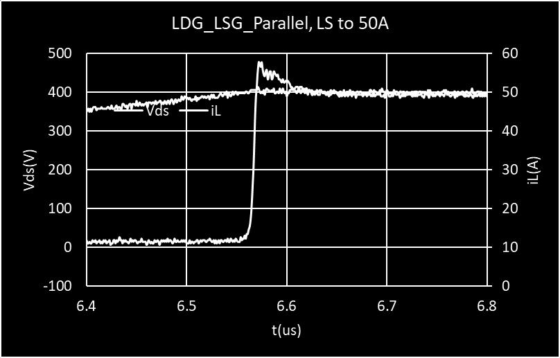
3 (c) Figure 4 High side device hard switching to 50A 50A switching waveform, the last turn-on switching waveform, (c) the last turn-off switching waveform (c) Figure 5 Low side device hard switching to 50A 50A switching waveform, the last turn-on switching waveform, (c) the last turn-off switching waveform 4. Efficiency Measurement and Calculation The efficiency is tested by configuring the halfbridge in synchronous rectification boost mode. The input voltage is 200V, output voltage is 400V and the circuit is an
4 switching at 50kHz or 100kHz with a 330 µh MPP core inductor. Figure 6 shows the efficiency curves, and the efficiency is over 99% at >1.25kW@50kHz and the efficiency is over 98.8% at >1.5kW@100kHz. The power rating at 100kHz is limited at 2.2kW due to the low side device case temperature rising to around 100 C, as shown in Figure 7. However, in the totem pole PFC application or full bridge inverters, the high side and low side devices will be operating in hard switching mode every half cycle, the switching loss can be evenly shared, therefore the temperature rising will be lower than boost converter. With the small SMD mounted heat sink, the paralleled PQFN is good to run over 2.5kW at the condition of high line and 100kHz switching frequency. as the turn-off loss is pretty small and it is relatively constant with no change with the current increasing. We can use the switching waveform with low side Vds and inductor current to do the calculation. Figure 6 Efficiency Measurement at 200Vin-400Vo, 50kHz and 100kHz Figure 8 A typical turn-on Vds and Ids waveform As shown in Figure 8, a typical turn-on waveform shows how the voltage and current change. In the first stage t1 period, the drain current will increase to the Irrm, and voltage across the drain and source will drop to Vdd2 due to the Lstray*di/dt, in the second stage t2 period, the Vds voltage will drop to zero and current goes down to the inductor current. We could not measure the drain current using regular low bandwidth current probe, but with the voltage and inductor current waveform and datasheet, we know Vdd, t1, t2, il, Qrr. The intermediate variable tr, ta, Irrm can be calculate as: tt aa = (ii LLtt 2 +2QQ rrrr )+ (ii LL tt 2 +2QQ rrrr ) 2 +8ii LL tt 1 QQ rrrr 2ii LL (1) tt rr = tt 1 tt aa (2) ii rrrrrr = 2QQ rrrr (3) tt aa +tt bb The turn-on loss can be described: EE oooo = 1 2 VV ddddii LL tt rr + VV dddd ii LL ii rrrrrr tt aa + VV dddd 1 2 ii LL ii rrrrrr tt bb Figure 7 Low side device case temprature at 100 CFM air flow condition The converter efficiency can also be estimated. The key part is to estimate the GaN FETs turn-on switching loss (4) Figure 9 shows the waveform at 5.2A turn-on. t1, t2 and Vdd2 are measured 9.6ns, 4.4ns and 220V, respectively, and the Qrr is 180nC@400V. The turn-on loss can be then estimated 58uJ. The Eon vs IL curve can be plotted in Figure 10, and the fitting equation is obtained. an

5 Figure 9 Vds and IL waveforms at low side device turn-on at 5.2A Figure 11 The measured efficiency vs estimated efficiency curve. Figure 10 The estimated turn-on energy for 2x70mΩ GenIII vs il at 400V The turn-off loss and high side device transition loss is small and constant around 23uJ. By carefully calculating other components losses, the converter efficiency curve can be plotted and the comparsion with measured result is shown in Figure 11. It is seen that the efficiency curve well match the measured curve. At light load, since the current drops to zero but Vds is not fully charged, the turn-on process is different from the hard-switching waveform, the estimated loss is a slightly lower. The loss breakdown is plotted in Figure 12 showing the losses on inductor, input/output capacitor, RC snubber circuit, and devices switching and conduction losses. an
6 Figure 12 Losses breakdown at 1.2kW Po and 2.5kW Po, fsw=50khz. Reference [1] AN0007: PQFN88 Lead-free 2nd Level Soldering Recommendations for Vapor Phase Reflow. Available: [2] AN0010: GaN FETs in Parallel Using Drain Ferrite Beads and RC Snubbers for High-power Applications. Available: an
Application Note 0009
 Recommended External Circuitry for Transphorm GaN FETs Application Note 9 Table of Contents Part I: Introduction... 2 Part II: Solutions to Suppress Oscillation... 2 Part III: The di/dt Limits of GaN Switching
VDSS (V) 650 V(TR)DSS (V) 800. RDS(on)eff (mω) max* 85. QRR (nc) typ 90. QG (nc) typ 10
 650 V(TR)DSS (V) 800. RDS(on)eff (mω) max* 85. QRR (nc) typ 90. QG (nc) typ 10") TP65H070L Series 650V GaN FET PQFN Series Preliminary Description The TP65H070L 650V, 72mΩ Gallium Nitride (GaN) FET are normally-off devices. It combines state-of-the-art high voltage GaN HEMT and low
TP65H070L Series 650V GaN FET PQFN Series Preliminary Description The TP65H070L 650V, 72mΩ Gallium Nitride (GaN) FET are normally-off devices. It combines state-of-the-art high voltage GaN HEMT and low
VDSS (V) 650 V(TR)DSS (V) 800 RDS(on)eff (mω) max* 180. QRR (nc) typ 47. QG (nc) typ 10
 650 V(TR)DSS (V) 800 RDS(on)eff (mω) max* 180. QRR (nc) typ 47. QG (nc) typ 10") TP65H150LSG 650V GaN FET PQFN Series Preliminary Datasheet Description The TP65H150LSG 650V, 150mΩ Gallium Nitride (GaN) FET are normally-off devices. They combine state-of-the-art high voltage GaN HEMT
TP65H150LSG 650V GaN FET PQFN Series Preliminary Datasheet Description The TP65H150LSG 650V, 150mΩ Gallium Nitride (GaN) FET are normally-off devices. They combine state-of-the-art high voltage GaN HEMT
VDSS (V) 650 V(TR)DSS (V) 800. RDS(on)eff (mω) max* 130. QRR (nc) typ 54. QG (nc) typ 10
 650 V(TR)DSS (V) 800. RDS(on)eff (mω) max* 130. QRR (nc) typ 54. QG (nc) typ 10") 650V GaN FET PQFN Series Not recommended for new designs Description The TPH3208L Series 650V, 110mΩ Gallium Nitride (GaN) FETs are normally-off devices. They combine state-of-the-art high voltage GaN
650V GaN FET PQFN Series Not recommended for new designs Description The TPH3208L Series 650V, 110mΩ Gallium Nitride (GaN) FETs are normally-off devices. They combine state-of-the-art high voltage GaN
VDSS (V) 650. V(TR)DSS (V) 800 RDS(on)eff (mω) max* 180. QRR (nc) typ 52. QG (nc) typ 6.2
 650. V(TR)DSS (V) 800 RDS(on)eff (mω) max* 180. QRR (nc) typ 52. QG (nc) typ 6.2") 650V GaN FET PQFN Series Not recommended for new designs Description The TPH3206L Series 650V, 150mΩ Gallium Nitride (GaN) FETs are normally-off devices. They combine state-of-the-art high voltage GaN
650V GaN FET PQFN Series Not recommended for new designs Description The TPH3206L Series 650V, 150mΩ Gallium Nitride (GaN) FETs are normally-off devices. They combine state-of-the-art high voltage GaN
VDSS (V) 650 V(TR)DSS (V) 800 RDS(on)eff (mω) max* 180. QRR (nc) typ 52. QG (nc) typ 6.2 VIN=230VAC; VOUT=390VDC VIN=380VDC; VOUT=240VAC
 650 V(TR)DSS (V) 800 RDS(on)eff (mω) max* 180. QRR (nc) typ 52. QG (nc) typ 6.2 VIN=230VAC; VOUT=390VDC VIN=380VDC; VOUT=240VAC") 650V GaN FET in TO-220 (source tab) Description The TPH3206PSB 650V, 150mΩ Gallium Nitride (GaN) FET is a normally-off device. It combines state-of-the-art high voltage GaN HEMT and low voltage silicon
650V GaN FET in TO-220 (source tab) Description The TPH3206PSB 650V, 150mΩ Gallium Nitride (GaN) FET is a normally-off device. It combines state-of-the-art high voltage GaN HEMT and low voltage silicon
VDSS (V) 650 V(TR)DSS (V) 800 RDS(on)eff (mω) max* 60. QRR (nc) typ 136. QG (nc) typ 28 VIN=230VAC; VOUT=390VDC VIN=380VDC; VOUT=240VAC
 650 V(TR)DSS (V) 800 RDS(on)eff (mω) max* 60. QRR (nc) typ 136. QG (nc) typ 28 VIN=230VAC; VOUT=390VDC VIN=380VDC; VOUT=240VAC") 650V GaN FET in TO-247 (source tab) Description The TPH3205WSB 650V, 49mΩ Gallium Nitride (GaN) FET is a normally-off device. It combines state-of-the-art high voltage GaN HEMT and low voltage silicon
650V GaN FET in TO-247 (source tab) Description The TPH3205WSB 650V, 49mΩ Gallium Nitride (GaN) FET is a normally-off device. It combines state-of-the-art high voltage GaN HEMT and low voltage silicon
VDSS (V) 900. V(TR)DSS (V) 1000 RDS(on)eff (mω) max* 205. QRR (nc) typ 49. QG (nc) typ 10
 900. V(TR)DSS (V) 1000 RDS(on)eff (mω) max* 205. QRR (nc) typ 49. QG (nc) typ 10") 900V GaN FET in TO-220 (source tab) Description The TP90H180PS 900V, 170mΩ Gallium Nitride (GaN) FET is a normally-off device. It combines state-of-the-art high voltage GaN HEMT and low voltage silicon
900V GaN FET in TO-220 (source tab) Description The TP90H180PS 900V, 170mΩ Gallium Nitride (GaN) FET is a normally-off device. It combines state-of-the-art high voltage GaN HEMT and low voltage silicon
Recommended External Circuitry for Transphorm GaN FETs. Zan Huang Jason Cuadra
 Recommended External Circuitry for Transphorm GaN FETs Zan Huang Jason Cuadra Application Note Rev. 1.0 November 22, 2016 Table of Contents 1 Introduction 3 2 Sustained oscillation 3 3 Solutions to suppress
VDSS (V) 650 V(TR)DSS (V) 800 RDS(on)eff (mω) max* 130. QRR (nc) typ 54. QG (nc) typ 14 VIN=230VAC; VOUT=390VDC VIN=380VDC; VOUT=240VAC
 650 V(TR)DSS (V) 800 RDS(on)eff (mω) max* 130. QRR (nc) typ 54. QG (nc) typ 14 VIN=230VAC; VOUT=390VDC VIN=380VDC; VOUT=240VAC") 650V GaN FET TO-220 Series Description The TPH3208PS 650V, 110mΩ Gallium Nitride (GaN) FET is a normally-off device. It combines state-of-the-art high voltage GaN HEMT and low voltage silicon MOSFET technologies
650V GaN FET TO-220 Series Description The TPH3208PS 650V, 110mΩ Gallium Nitride (GaN) FET is a normally-off device. It combines state-of-the-art high voltage GaN HEMT and low voltage silicon MOSFET technologies
235 W Maximum Power Dissipation (whole module) 470 T J Junction Operating Temperature -40 to 150. Torque strength
 470 T J Junction Operating Temperature -40 to 150. Torque strength") Discontinued PRODUCT SUMMARY (TYPICAL) V DS (V) 600 R DS(on) (m ) 30 GaN Power Hybrid HEMT Half-Bridge Module Features High frequency operation Free-wheeling diode not required Applications Compact DC-DC
Discontinued PRODUCT SUMMARY (TYPICAL) V DS (V) 600 R DS(on) (m ) 30 GaN Power Hybrid HEMT Half-Bridge Module Features High frequency operation Free-wheeling diode not required Applications Compact DC-DC
PRELIMINARY. VDSS (V) 600 V(TR)DSS (V) 750 RDS(on)eff (mω) max* 60. QRR (nc) typ 120. QG (nc) typ 22 PRELIMINARY
 600 V(TR)DSS (V) 750 RDS(on)eff (mω) max* 60. QRR (nc) typ 120. QG (nc) typ 22 PRELIMINARY") PRELIMINARY TPH3205ESBET 600V GaN FET in TO-268 (source tab) Description The TPH3205ESBET 600V, 49mΩ Gallium Nitride (GaN) FET is a normally-off device. It combines state-of-the-art high voltage GaN HEMT
PRELIMINARY TPH3205ESBET 600V GaN FET in TO-268 (source tab) Description The TPH3205ESBET 600V, 49mΩ Gallium Nitride (GaN) FET is a normally-off device. It combines state-of-the-art high voltage GaN HEMT
Designing reliable and high density power solutions with GaN. Created by: Masoud Beheshti Presented by: Paul L Brohlin
 Designing reliable and high density power solutions with GaN Created by: Masoud Beheshti Presented by: Paul L Brohlin What will I get out of this presentation? Why GaN? Integration for System Performance
Symbol Parameter Typical
 PRODUCT SUMMARY (TYPICAL) V DS (V) 650 R DS(on) (m ) 110 Q rr (nc) 54 Features Low Q rr Free-wheeling diode not required Low-side Quiet Tab for reduced EMI RoHS compliant High frequency operation Applications
VDS (V) min 650 VTDS (V) max 800 RDS(on) (mω) max* 60. Qrr (nc) typ 136. Qg (nc) typ 28. * Dynamic RDS(on)
 min 650 VTDS (V) max 800 RDS(on) (mω) max* 60. Qrr (nc) typ 136. Qg (nc) typ 28. * Dynamic RDS(on)") 650V Cascode GaN FET in TO-247 (source tab) Description The TPH3205WSB 650V, 49mΩ gallium nitride (GaN) FET is a normally-off device. Transphorm GaN FETs offer better efficiency through lower gate charge,
650V Cascode GaN FET in TO-247 (source tab) Description The TPH3205WSB 650V, 49mΩ gallium nitride (GaN) FET is a normally-off device. Transphorm GaN FETs offer better efficiency through lower gate charge,
VDS (V) min 650 VTDS (V) max 800 RDS(on) (mω) max* 130. Qrr (nc) typ 54. * Dynamic R(on)
 min 650 VTDS (V) max 800 RDS(on) (mω) max* 130. Qrr (nc) typ 54. * Dynamic R(on)") 650V Cascode GaN FET in TO-220 (source tab) Description The TPH3208PS 650V, 110mΩ gallium nitride (GaN) FET is a normally-off device. Transphorm GaN FETs offer better efficiency through lower gate charge,
650V Cascode GaN FET in TO-220 (source tab) Description The TPH3208PS 650V, 110mΩ gallium nitride (GaN) FET is a normally-off device. Transphorm GaN FETs offer better efficiency through lower gate charge,
Application Note 0006
 VGS Transient Tolerance of Transphorm GaN FETs Abstract This document provides a guideline for allowable transient voltages between gate and source pins. Table of Contents Abstract... 1 Introduction...
Demands for High-efficiency Magnetics in GaN Power Electronics
 APEC 2014, Fort Worth, Texas, March 16-20, 2014, IS2.5.3 Demands for High-efficiency Magnetics in GaN Power Electronics Yifeng Wu, Transphorm Inc. Table of Contents 1. 1 st generation 600V GaN-on-Si HEMT
Drive and Layout Requirements for Fast Switching High Voltage MOSFETs
 Drive and Layout Requirements for Fast Switching High Voltage MOSFETs Contents Introduction SuperJunction Technologies Influence of Circuit Parameters on Switching Characteristics Gate Resistance Clamp
Designing High density Power Solutions with GaN Created by: Masoud Beheshti Presented by: Xaver Arbinger
 Designing High density Power Solutions with GaN Created by: Masoud Beheshti Presented by: Xaver Arbinger Topics Why GaN? Integration for Higher System Performance Application Examples Taking GaN beyond
Symbol Parameter Typical
 PRODUCT SUMMARY (TYPICAL) V DS (V) 600 R DS(on) ( ) 0.29 Q rr (nc) 29 Features Low Q rr Free-wheeling diode not required Low-side Quiet Tab for reduced EMI RoHS compliant High frequency operation Applications
TPH3205WSB. 650V Cascode GaN FET in TO-247 (source tab)
") 650V Cascode GaN FET in TO-247 (source tab) Description The TPH3205WSB 650V, 52mΩ gallium nitride (GaN) FET is a normally-off device. Transphorm GaN FETs offer better efficiency through lower gate charge,
650V Cascode GaN FET in TO-247 (source tab) Description The TPH3205WSB 650V, 52mΩ gallium nitride (GaN) FET is a normally-off device. Transphorm GaN FETs offer better efficiency through lower gate charge,
Practical Design Considerations for a 3.3kW Bridgeless Totem-pole PFC Using GaN FETs. Jim Honea Transphorm Inc
 Practical Design Considerations for a 3.3kW Bridgeless Totem-pole PFC Using GaN FETs Jim Honea Transphorm Inc Overview of the Circuit Specifications 3.3kW (max) CCM bridgeless totem-pole PFC, Universal
GS66516T Top-side cooled 650 V E-mode GaN transistor Preliminary Datasheet
 Features 650 V enhancement mode power switch Top-side cooled configuration R DS(on) = 25 mω I DS(max) = 60 A Ultra-low FOM Island Technology die Low inductance GaNPX package Easy gate drive requirements
TPH3207WS TPH3207WS. GaN Power Low-loss Switch PRODUCT SUMMARY (TYPICAL) Absolute Maximum Ratings (T C =25 C unless otherwise stated)
 Absolute Maximum Ratings (T C =25 C unless otherwise stated)") PRODUCT SUMMARY (TYPICAL) V DS (V) 650 R DS(on) (m ) 35 Q rr (nc) 175 Features Low Q rr Free-wheeling diode not required Quiet Tab for reduced EMI at high dv/dt GSD pin layout improves high speed design
PRODUCT SUMMARY (TYPICAL) V DS (V) 650 R DS(on) (m ) 35 Q rr (nc) 175 Features Low Q rr Free-wheeling diode not required Quiet Tab for reduced EMI at high dv/dt GSD pin layout improves high speed design
Unlocking the Power of GaN PSMA Semiconductor Committee Industry Session
 Unlocking the Power of GaN PSMA Semiconductor Committee Industry Session March 24 th 2016 Dan Kinzer, COO/CTO dan.kinzer@navitassemi.com 1 Mobility (cm 2 /Vs) EBR Field (MV/cm) GaN vs. Si WBG GaN material
LD /07/ Channel LED Backlight Driver. General Description. Features. Applications. Typical Application REV: 05
 10/07/2011 4 Channel LED Backlight Driver REV: 05 General Description The LD7889 is a 4-channel linear current controller which combines with a boost switching controller. It s an ideal solution for driving
VDS (V) min 600 VTDS (V) max 750 RDS(on) (mω) max* 63. Qrr (nc) typ 136. * Dynamic R(on)
 min 600 VTDS (V) max 750 RDS(on) (mω) max* 63. Qrr (nc) typ 136. * Dynamic R(on)") 600V Cascode GaN FET in TO-247 (source tab) Not recommended for new designs see TP65H050WS Description The TPH3205WS 600V, 52mΩ gallium nitride (GaN) FET is a normally-off device. Transphorm GaN FETs offer
600V Cascode GaN FET in TO-247 (source tab) Not recommended for new designs see TP65H050WS Description The TPH3205WS 600V, 52mΩ gallium nitride (GaN) FET is a normally-off device. Transphorm GaN FETs offer
Breaking Speed Limits with GaN Power ICs March 21 st 2016 Dan Kinzer, COO/CTO
 Breaking Speed Limits with GaN Power ICs March 21 st 2016 Dan Kinzer, COO/CTO dan.kinzer@navitassemi.com 1 Efficiency The Need for Speed Tomorrow? Today 100kHz 1MHz 10MHz Bulky, Heavy Small, Light & Expensive
Get Your GaN PhD in Less Than 60 Minutes!
 Get Your GaN PhD in Less Than 60 Minutes! 1 Detailed agenda Why is GaN Exciting GaN Fundamentals Cost and Reliability Totem Pole PFC Isolated LLC Motor Drive LiDAR Driving GaN Choosing a GaN Tools 4 Why
SiC Transistor Basics: FAQs
 SiC Transistor Basics: FAQs Silicon Carbide (SiC) MOSFETs exhibit higher blocking voltage, lower on state resistance and higher thermal conductivity than their silicon counterparts. Oct. 9, 2013 Sam Davis
GaN in Practical Applications
 in Practical Applications 1 CCM Totem Pole PFC 2 PFC: applications and topology Typical AC/DC PSU 85-265 V AC 400V DC for industrial, medical, PFC LLC 12, 24, 48V DC telecomm and server applications. PFC
TPH3212PS. 650V Cascode GaN FET in TO-220 (source tab)
") 650V Cascode GaN FET in TO-220 (source tab) Description The TPH3212PS 650V, 72mΩ gallium nitride (GaN) FET is a normally-off device. Transphorm GaN FETs offer better efficiency through lower gate charge,
650V Cascode GaN FET in TO-220 (source tab) Description The TPH3212PS 650V, 72mΩ gallium nitride (GaN) FET is a normally-off device. Transphorm GaN FETs offer better efficiency through lower gate charge,
GS66508P Bottom-side cooled 650 V E-mode GaN transistor Preliminary Datasheet
 Features 650 V enhancement mode power switch Bottom-side cooled configuration R DS(on) = 50 mω I DS(max) = 30 A Ultra-low FOM Island Technology die Low inductance GaNPX package Easy gate drive requirements
PXD30-xxWS-xx-Single Output DC/DC Converters
 PXD30-xxWS-xx-Single Output DC/DC Converters 9 to 36 Vdc and 18 to 75 Vdc input, 1.5 to 15 Vdc Single Output, 30W Applications Wireless Network Telecom / Datacom Industry Control System Measurement Semiconductor
GS66508T Top-side cooled 650 V E-mode GaN transistor Preliminary Datasheet
 Features 650 V enhancement mode power switch Top-side cooled configuration R DS(on) = 50 mω I DS(max) = 30 A Ultra-low FOM Island Technology die Low inductance GaNPX package Easy gate drive requirements
GS66508T Top-side cooled 650 V E-mode GaN transistor Preliminary Datasheet
 Features 650 V enhancement mode power switch Top-side cooled configuration R DS(on) = 50 mω I DS(max) = 30 A Ultra-low FOM Island Technology die Low inductance GaNPX package Easy gate drive requirements
Power of GaN. Enabling designers to create smaller, more efficient and higher-performing AC/DC power supplies
 Power of GaN Enabling designers to create smaller, more efficient and higher-performing AC/DC power supplies Steve Tom Product Line Manager, GaN Products stom@ti.com Solving power and energy-management
An Experimental Comparison of GaN E- HEMTs versus SiC MOSFETs over Different Operating Temperatures
 An Experimental Comparison of GaN E- HEMTs versus SiC MOSFETs over Different Operating Temperatures Jianchun Xu, Yajie Qiu, Di Chen, Juncheng Lu, Ruoyu Hou, Peter Di Maso GaN Systems Inc. Ottawa, Canada
Designing a 99% Efficient Totem Pole PFC with GaN. Serkan Dusmez, Systems and applications engineer
 Designing a 99% Efficient Totem Pole PFC with GaN Serkan Dusmez, Systems and applications engineer 1 What will I get out of this session? Purpose: Why GaN Based Totem-pole PFC? Design guidelines for getting
Features. Description. Table 1: Device summary Order code Marking Package Packing STD30NF06LAG D30NF06L DPAK Tape and reel
 Automotive-grade N-channel 60 V, 0.022 Ω typ., 35 A STripFET II Power MOSFET in a DPAK package Datasheet - production data Features Order code VDS RDS(on) max. ID STD30NF06LAG 60 V 0.028 Ω 35 A AEC-Q101
GS66508T Top-side cooled 650 V E-mode GaN transistor Preliminary Datasheet
 Features 650 V enhancement mode power switch Top-side cooled configuration R DS(on) = 50 mω I DS(max) = 30 A Ultra-low FOM Island Technology die Low inductance GaNPX package Easy gate drive requirements
User s Manual ISL70040SEHEV2Z. User s Manual: Evaluation Board. High Reliability
 User s Manual ISL70040SEHEV2Z User s Manual: Evaluation Board High Reliability Rev 0.00 Nov 2017 USER S MANUAL ISL70040SEHEV2Z Evaluation Board for the ISL70040SEH and ISL70023SEH UG147 Rev.0.00 1. Overview
N-channel 100 V, 9.0 mω typ., 110 A STripFET II Power MOSFETs in D²PAK, TO-220 and TO-247 packages. Features. Description
 STB120NF10T4, STP120NF10, STW120NF10 N-channel 100 V, 9.0 mω typ., 110 A STripFET II Power MOSFETs in D²PAK, TO-220 and TO-247 packages Datasheet - production data TAB Features Order code VDS RDS(on) max.
Features. Description. Table 1: Device summary Order code Marking Package Packing STD20NF06LAG D20N6LF6 DPAK Tape and Reel
 Automotive-grade N-channel 60 V, 32 mω typ., 24 A STripFET II Power MOSFET in a DPAK package Datasheet - production data Features Order code VDS RDS(on) max. ID PTOT STD20NF06LAG 60 V 40 mω 24 A 60 W AEC-Q101
Gate Drive Optimisation
 Gate Drive Optimisation 1. Background Driving of gates of MOSFET, IGBT and SiC/GaN switching devices is a fundamental requirement in power conversion. In the case of ground-referenced drives this is relatively
User s Manual ISL70040SEHEV3Z. User s Manual: Evaluation Board. High Reliability
 User s Manual ISL70040SEHEV3Z User s Manual: Evaluation Board High Reliability Rev 0.00 Nov 2017 USER S MANUAL ISL70040SEHEV3Z Evaluation Board for the ISL70040SEH and ISL70024SEH UG146 Rev.0.00 1. Overview
GS66508B Bottom-side cooled 650 V E-mode GaN transistor Preliminary Datasheet
 Features 650 V enhancement mode power switch Bottom-side cooled configuration R DS(on) = 50 mω I DS(max) = 30 A Ultra-low FOM Island Technology die Low inductance GaNPX package Easy gate drive requirements
Revision. 007 PGA26E19BA. Product Standards PGA26E19BA. Established: Revised: Page 1 of 11
 Revision. 7 Product Standards Established: 24-9-25 Revised: 27--24 Page of Revision. 7 Type Application Structure GaN-Tr For power switching N-channel enhancement mode FET Equivalent Circuit Figure Out
STB13N60M2, STD13N60M2
 STB13N60M2, STD13N60M2 N-channel 600 V, 0.35 Ω typ., 11 A MDmesh M2 Power MOSFETs in D 2 PAK and DPAK packages Datasheet - production data Features Order code VDS@TJMAX. RDS(on) max. ID STB13N60M2 STD13N60M2
IRLR8721PbF IRLU8721PbF
 Applications l High Frequency Synchronous Buck Converters for Computer Processor Power l High Frequency Isolated DC-DC Converters with Synchronous Rectification for Telecom and Industrial Use l Lead-Free
Wide Band-Gap (SiC and GaN) Devices Characteristics and Applications. Richard McMahon University of Cambridge
 Devices Characteristics and Applications. Richard McMahon University of Cambridge") Wide Band-Gap (SiC and GaN) Devices Characteristics and Applications Richard McMahon University of Cambridge Wide band-gap power devices SiC : MOSFET JFET Schottky Diodes Unipolar BJT? Bipolar GaN : FET
Wide Band-Gap (SiC and GaN) Devices Characteristics and Applications Richard McMahon University of Cambridge Wide band-gap power devices SiC : MOSFET JFET Schottky Diodes Unipolar BJT? Bipolar GaN : FET
VDS (V) min 600 VTDS (V) max 750 RDS(on) (mω) max* 180. Qrr (nc) typ 54. * Dynamic R(on)
 min 600 VTDS (V) max 750 RDS(on) (mω) max* 180. Qrr (nc) typ 54. * Dynamic R(on)") 600V Cascode GaN FET in TO-220 (drain tab) Description The 600V, 150mΩ gallium nitride (GaN) FET is a normally-off device. Transphorm GaN FETs offer better efficiency through lower gate charge, faster
600V Cascode GaN FET in TO-220 (drain tab) Description The 600V, 150mΩ gallium nitride (GaN) FET is a normally-off device. Transphorm GaN FETs offer better efficiency through lower gate charge, faster
GS66506T Top-side cooled 650 V E-mode GaN transistor Preliminary Datasheet
 Features 650 V enhancement mode power switch Top-side cooled configuration R DS(on) = 67 mω I DS(max) = 22.5 A Ultra-low FOM Island Technology die Low inductance GaNPX package Easy gate drive requirements
ANP030. Contents. Application Note AP2014/A Synchronous PWM Controller. 1. AP2014/A Specification. 2. Hardware. 3. Design Procedure. 4.
 Contents 1. AP2014/A Specification 1.1 Features 1.2 General Description 1.3 Pin Assignments 1.4 Pin Descriptions 1.5 Block Diagram 1.6 Absolute Maximum Ratings 2. Hardware 2.1 Introduction 2.2 Description
TPH3202PS TPH3202PS. GaN Power Low-loss Switch PRODUCT SUMMARY (TYPICAL) TO-220 Package. Absolute Maximum Ratings (T C =25 C unless otherwise stated)
 TO-220 Package. Absolute Maximum Ratings (T C =25 C unless otherwise stated)") PRODUCT SUMMARY (TYPICAL) V DS (V) 600 R DS(on) ( ) 0.29 Q rr (nc) 29 Features Low Q rr Free-wheeling diode not required Low-side Quiet Tab for reduced EMI GSD pin layout improves high speed design RoHS
PRODUCT SUMMARY (TYPICAL) V DS (V) 600 R DS(on) ( ) 0.29 Q rr (nc) 29 Features Low Q rr Free-wheeling diode not required Low-side Quiet Tab for reduced EMI GSD pin layout improves high speed design RoHS
SiC Cascodes and its advantages in power electronic applications
 SiC Cascodes and its advantages in power electronic applications WBG Power Conference, Munich, 5 th December 2017 Christopher Rocneanu Director Sales Europe and North America cro@unitedsic.com +4915121063411
LD7889A 3/29/ Channel LED Backlight Driver. General Description. Features. Applications. Typical Application REV: 00
 3/29/2012 4-Channel LED Backlight Driver REV: 00 General Description The LD7889A is a 4-channel linear current controller which combines with a boost switching controller. It s an ideal solution for driving
HCD80R600R 800V N-Channel Super Junction MOSFET
 HCD80R600R 800V N-Channel Super Junction MOSFET Features Very Low FOM (R DS(on) X Q g ) Extremely low switching loss Excellent stability and uniformity 00% Avalanche Tested Application Switch Mode Power
Pitch Pack Microsemi full SiC Power Modules
 Pitch Pack Microsemi full SiC Power Modules October 2014 SiC Main Characteristics vs. Si Characteristics SiC vs. Si Results Benefits Breakdown field (MV/cm) Electron sat. velocity (cm/s) Bandgap energy
Features. Description. Table 1: Device summary Order code Marking Package Packing STN3NF06L 3NF06L SOT-223 Tape and reel
 N-channel 60 V, 0.07 Ω typ., 4 A STripFET II Power MOSFET in a SOT-223 package Datasheet - production data Features Order code VDS RDS(on) max. ID STN3NF06L 60 V 0.1 Ω 4 A Exceptional dv/dt capability
IRFR3709ZPbF IRFU3709ZPbF
 Applications l High Frequency Synchronous Buck Converters for Computer Processor Power l High Frequency Isolated DC-DC Converters with Synchronous Rectification for Telecom and Industrial Use l Lead-Free
Pin Configurations Package Pin Configurations LX 1 5 V IN SOT ADJ 3 4 I SENSE SOT89-5 Pin Description Pin Name NO. Description LX 1 Drain of pow
 700mA LED driver with internal switch General Description The is a continuous mode inductive step-down converter, designed for driving a single LED or multiple series connected LEDs efficiently from a
Features. Description. Table 1: Device summary Order code Marking Package Packing STL10N65M2 10N65M2 PowerFLAT 5x6 HV Tape and reel
 N-channel 650 V, 0.85 Ω typ., 4.5 A MDmesh M2 Power MOSFET in a PowerFLAT 5x6 HV package Datasheet - production data Features Order code VDS RDS(on) max. ID STL10N65M2 650 V 1.00 Ω 4.5 A 1 2 3 4 PowerFLAT
V DSS R DS(on) max Qg. 560 P C = 25 C Maximum Power Dissipation g 140 P C = 100 C Maximum Power Dissipation g Linear Derating Factor
 max Qg. 560 P C = 25 C Maximum Power Dissipation g 140 P C = 100 C Maximum Power Dissipation g Linear Derating Factor") Applications l High Frequency Synchronous Buck Converters for Computer Processor Power l High Frequency Isolated DC-DC Converters with Synchronous Rectification for Telecom and Industrial Use Benefits
Applications l High Frequency Synchronous Buck Converters for Computer Processor Power l High Frequency Isolated DC-DC Converters with Synchronous Rectification for Telecom and Industrial Use Benefits
GS66502B Bottom-side cooled 650 V E-mode GaN transistor Preliminary Datasheet
 GS66502B Features 650 V enhancement mode power switch Bottom-side cooled configuration R DS(on) = 200 mω I DS(max) = 7.5 A Ultra-low FOM Island Technology die Low inductance GaNPX package Easy gate drive
GS66516B Bottom-side cooled 650 V E-mode GaN transistor Preliminary Datasheet
 Features 650 V enhancement mode power switch Bottom-side cooled configuration R DS(on) = 25 mω I DS(max) = 60 A Ultra-low FOM Island Technology die Low inductance GaNPX package Easy gate drive requirements
AN2649 Application note
 Application note A power factor corrector with MDmesh TM II and SiC diode Introduction The electrical and thermal performances of switching converters are strongly influenced by the behavior of the switching
5.0V 5.0V. 20µs PULSE WIDTH Tj = 25 C. Tj = 150 C. V DS, Drain-to-Source Voltage (V) T J = 150 C 1.5. V GS, Gate-to-Source Voltage (V)
 T J = 150 C 1.5. V GS, Gate-to-Source Voltage (V)") 9MT050XF "FULL-BRIDGE" FREDFET MTP HEXFET Power MOSFET Features Low On-Resistance High Performance Optimised Built-in Fast Recovery Diodes Fully Characterized Capacitance and Avalanche Voltage and Current
9MT050XF "FULL-BRIDGE" FREDFET MTP HEXFET Power MOSFET Features Low On-Resistance High Performance Optimised Built-in Fast Recovery Diodes Fully Characterized Capacitance and Avalanche Voltage and Current
N-channel 600 V, Ω typ., 34 A MDmesh M2 EP Power MOSFETs in D²PAK, TO-220 and TO-247 packages. Features STW42N60M2-EP.
 N-channel 600 V, 0.076 Ω typ., 34 A MDmesh M2 EP Power MOSFETs in D²PAK, TO-220 and TO-247 packages Datasheet - production data Features TAB TAB Order code VDS @ TJmax RDS(on) max. ID STB42N60M2-EP D²PAK
HCD80R1K4E 800V N-Channel Super Junction MOSFET
 HCD80R1K4E 800V N-Channel Super Junction MOSFET Features Very Low FOM (R DS(on) X Q g ) Extremely low switching loss Excellent stability and uniformity 100% Avalanche Tested Application Switch Mode Power
MIC4414/4415. General Description. Features. Applications. Typical Application. 1.5A, 4.5V to 18V, Low-Side MOSFET Driver
 MIC4414/4415 1.5A, 4.5V to 18V, Low-Side MOSFET Driver General Description The MIC4414 and MIC4415 are low-side MOSFET drivers designed to switch an N-channel enhancement type MOSFET in low-side switch
V DSS R DS(on) max Qg
 max Qg") Applications l High Frequency Synchronous Buck Converters for Computer Processor Power l High Frequency Isolated DC-DC Converters with Synchronous Rectification for Telecom and Industrial Use l Lead-Free
Applications l High Frequency Synchronous Buck Converters for Computer Processor Power l High Frequency Isolated DC-DC Converters with Synchronous Rectification for Telecom and Industrial Use l Lead-Free
TO-220 G D S. T C = 25 C unless otherwise noted
 500V N-Channel MOSFET General Description This Power MOSFET is produced using Maple semi s advanced planar stripe DMOS technology. This advanced technology has been especially tailored to minimize on-state
HCD80R650E 800V N-Channel Super Junction MOSFET
 HCD80R650E 800V N-Channel Super Junction MOSFET Features Very Low FOM (R DS(on) X Q g ) Extremely low switching loss Excellent stability and uniformity 100% Avalanche Tested Application Switch Mode Power
ThinPAK 8x8. New High Voltage SMD-Package. April 2010 Version 1.0
 ThinPAK 8x8 New High Voltage SMD-Package Version 1.0 Content Introduction Package Specification Thermal Concept Application Test Conditions Impact on Efficiency and EMI Switching behaviour Portfolio and
Features MIC2193BM. Si9803 ( 2) 6.3V ( 2) VDD OUTP COMP OUTN. Si9804 ( 2) Adjustable Output Synchronous Buck Converter
 6.3V ( 2) VDD OUTP COMP OUTN. Si9804 ( 2) Adjustable Output Synchronous Buck Converter") MIC2193 4kHz SO-8 Synchronous Buck Control IC General Description s MIC2193 is a high efficiency, PWM synchronous buck control IC housed in the SO-8 package. Its 2.9V to 14V input voltage range allows
MIC2193 4kHz SO-8 Synchronous Buck Control IC General Description s MIC2193 is a high efficiency, PWM synchronous buck control IC housed in the SO-8 package. Its 2.9V to 14V input voltage range allows
HEXFET MOSFET TECHNOLOGY
 PD-91551D POWER MOSFET SURFACE MOUNT(SMD-1) Product Summary Part Number RDS(on) ID IRFN350 0.315 Ω 14A IRFN350 JANTX2N7227U JANTXV2N7227U REF:MIL-PRF-19500/592 400V, N-CHANNEL HEXFET MOSFET TECHNOLOGY
Application Note AN-1199
 Application Note AN-1199 Sensing Current with IR25750 By T. Ribarich Table of Contents Topic Page 1. Introduction..... 2 2. IR25750 Functional Description. 3 3. MOSFET VDS(on) Sensing.. 5 4. IGBT VCE(on)
8 S1, D2. Storage Temperature Range Soldering Temperature, for 10 seconds 300 (1.6mm from case )
") Co-Pack Dual N-channel HEXFET Power MOSFET and Schottky Diode Ideal for Synchronous Buck DC-DC Converters Up to A Peak Output Low Conduction Losses Low Switching Losses Low Vf Schottky Rectifier D D 2
Co-Pack Dual N-channel HEXFET Power MOSFET and Schottky Diode Ideal for Synchronous Buck DC-DC Converters Up to A Peak Output Low Conduction Losses Low Switching Losses Low Vf Schottky Rectifier D D 2
1.5MHz, 3A Synchronous Step-Down Regulator
 1.5MHz, 3A Synchronous Step-Down Regulator FP6165 General Description The FP6165 is a high efficiency current mode synchronous buck PWM DC-DC regulator. The internal generated 0.6V precision feedback reference
A Solution to Simplify 60A Multiphase Designs By John Lambert & Chris Bull, International Rectifier, USA
 A Solution to Simplify 60A Multiphase Designs By John Lambert & Chris Bull, International Rectifier, USA As presented at PCIM 2001 Today s servers and high-end desktop computer CPUs require peak currents
HCA60R080FT (Fast Recovery Diode Type) 600V N-Channel Super Junction MOSFET
 600V N-Channel Super Junction MOSFET") HCA60R080FT (Fast Recovery Diode Type) 600V N-Channel Super Junction MOSFET Features Very Low FOM (R DS(on) X Q g ) Extremely low switching loss Excellent stability and uniformity 00% Avalanche Tested
HCA60R080FT (Fast Recovery Diode Type) 600V N-Channel Super Junction MOSFET Features Very Low FOM (R DS(on) X Q g ) Extremely low switching loss Excellent stability and uniformity 00% Avalanche Tested
Features. Description. Table 1: Device summary Order code Marking Package Packing STW48N60M2-4 48N60M2 TO247-4 Tube
 N-channel 600 V, 0.06 Ω typ., 42 A MDmesh M2 Power MOSFET in a TO247-4 package Datasheet - production data Features Order code V DS @ T Jmax. R DS(on)max. I D STW48N60M2-4 650 V 0.07 Ω 42 A Excellent switching
Making Reliable and High-Density GaN Solutions a Reality
 Making Reliable and High-Density GaN Solutions a Reality December 5, 2017 Franz Xaver Arbinger Masoud Beheshti 1 Today s Topics Why is GaN Exciting GaN Fundamentals Cost and Reliability Totem Pole PFC
Features. Description. Table 1: Device summary Order code Marking Package Packing STB20N90K5 20N90K5 D²PAK Tape and reel
 N-channel 900 V, 0.21 Ω typ., 20 A MDmesh K5 Power MOSFET in a D²PAK package Datasheet - production data Features TAB Order code VDS RDS(on) max. ID STB20N90K5 900 V 0.25 Ω 20 A 2 3 1 D²PAK Industry s
HCS80R1K4E 800V N-Channel Super Junction MOSFET
 HCS80R1K4E 800V N-Channel Super Junction MOSFET Features Very Low FOM (R DS(on) X Q g ) Extremely low switching loss Excellent stability and uniformity 100% Avalanche Tested Application Switch Mode Power
Advanced Silicon Devices Applications and Technology Trends
 Advanced Silicon Devices Applications and Technology Trends Gerald Deboy Winfried Kaindl, Uwe Kirchner, Matteo Kutschak, Eric Persson, Michael Treu APEC 2015 Content Silicon devices versus GaN devices:
IRLR3717 IRLU3717 HEXFET Power MOSFET
 Applications l High Frequency Synchronous Buck Converters for Computer Processor Power l High Frequency Isolated DC-DC Converters with Synchronous Rectification for Telecom and Industrial Use PD - 94718B
MADR TR. Quad Driver for GaAs FET or PIN Diode Switches and Attenuators Rev. 4. Functional Schematic. Features.
 Features High Voltage CMOS Technology Four Channel Positive Voltage Control CMOS device using TTL input levels Low Power Dissipation Low Cost Lead-Free SOIC-16 Plastic Package Halogen-Free Green Mold Compound
N-channel 650 V, Ω typ., 16 A MDmesh M2 Power MOSFET in D2PAK, TO-220FP and TO-220 packages. Features STP24N65M2.
 STB24N65M2, STF24N65M2, STP24N65M2 N-channel 650 V, 0.185 Ω typ., 16 A MDmesh M2 Power MOSFET in D2PAK, TO-220FP and TO-220 packages Datasheet - production data Features Order codes VDS RDS(on) max ID
SSP20N60S / SSF20N60S 600V N-Channel MOSFET
 SSP20N60S / SSF20N60S 600V N-Channel MOSFET Description SJ-FET is new generation of high voltage MOSFET family that is utilizing an advanced charge balance mechanism for outstanding low on-resistance and
2N7620M2 THRU-HOLE (14-LEAD FLAT PACK) TECHNOLOGY. Product Summary
 TECHNOLOGY. Product Summary") PD-9735 RADIATION HARDENED LOGIC LEVEL POWER MOSFET THRU-HOLE (4-LEAD FLAT PACK) Product Summary Part Number Radiation Level RDS(on) ID IRHLA77Z4 K Rads (Si).6Ω.8A IRHLA73Z4 3K Rads (Si).6Ω.8A 2N762M2
PD-9735 RADIATION HARDENED LOGIC LEVEL POWER MOSFET THRU-HOLE (4-LEAD FLAT PACK) Product Summary Part Number Radiation Level RDS(on) ID IRHLA77Z4 K Rads (Si).6Ω.8A IRHLA73Z4 3K Rads (Si).6Ω.8A 2N762M2
DC/DC Converter 9 to 36Vdc and 18 to 75Vdc input voltage, 20 Watt Output Power; 3.3 to 15Vdc Single Output and ±12Vdc to ±15Vdc Dual Output
 THN 20WI Series Application Note DC/DC Converter 9 to 36Vdc and 18 to 75Vdc input voltage, 20 Watt Output Power; 3.3 to 15Vdc Single Output and ±12Vdc to ±15Vdc Dual Output Pending Applications Wireless
Application Note MHz, Class D Push-Pull, 1.7KW RF Generator with Microsemi DRF1300 Power MOSFET Hybrid
 13.56 MHz, Class D Push-Pull, 1.7KW RF Generator with Microsemi DRF1300 Power MOSFET Hybrid June 26, 2008 By Gui Choi Sr. RF Application Engineer The DRF1300/CLASS-D Reference design is available to expedite
DP9126IX. Non-Isolated Buck APFC Offline LED Power Switch FEATURES GENERAL DESCRIPTION APPLICATIONS TYPICAL APPLICATION CIRCUIT
 Non-Isolated Buck APFC Offline LED Power Switch DP9126IX FEATURES Active PFC for High PF and Low THD PF>0.9 with Universal Input Built-in HV Startup and IC Power Supply Circuit Internal 650V Power MOSFET
IR3101 Series 1.6A, 500V
 Half-Bridge FredFet and Integrated Driver Features Output power FredFets in half-bridge configuration High side gate drive designed for bootstrap operation Bootstrap diode integrated into package. Lower
HCS80R380R 800V N-Channel Super Junction MOSFET
 HCS8R38R 8V N-Channel Super Junction MOSFET Features Very Low FOM (R DS(on) X Q g ) Extremely low switching loss Excellent stability and uniformity % Avalanche Tested Application Switch Mode Power Supply
Features. Description. AM15572v1. Table 1. Device summary. Order codes Marking Package Packaging. STD13N65M2 13N65M2 DPAK Tape and reel
 N-channel 650 V, 0.37 Ω typ., 10 A MDmesh M2 Power MOSFET in a DPAK package Features Datasheet production data TAB 2 3 1 DPAK Figure 1. Internal schematic diagram, TAB Order code V DS R DS(on) max I D
RC-D Fast : RC-Drives IGBT optimized for high switching frequency
 RC-D Fast : RC-Drives IGBT optimized for high switching frequency Application Note Application Engineering IGBT July 2012, Mitja Rebec Power Management 1 Discretes Published by Infineon Technologies AG