My USM. Mustafa G. Guvench. Professor, Electrical Engineering
|
|
|
- Frederica Nicholson
- 5 years ago
- Views:
Transcription


1 My USM Mustafa G. Guvench Professor, Electrical Engineering
2 My Interests & Expertise CMOS Analog I.C. Design Silicon I.C. Processing Micro Machining and MEMS Optoelectronics (Photosensors( Photosensors) SENSORS (MEMS, Semiconductor) Instrumentation and Measurement
3 Courses I teach CMOS Analog I.C. Design ELE 444 Silicon I.C. Processing ELE 464 Optoelectronics ELE 467 Electronics I & II ELE 342&343 Others ELE


4 CMOS Analog Chip Design
 M.G.")
5 CMOS Analog Chip Design (Operational Amplifier) M.G.Guvench
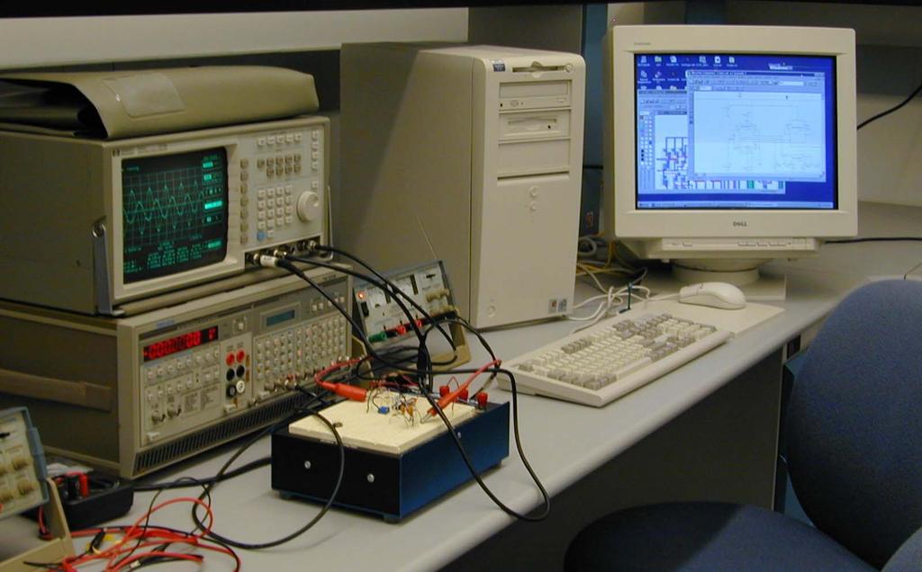
6 The Measurement System


7 MicroFab Laboratory I-V Characterization System

8 The Measurement System is used for Automated Measurement of Semi. Device Chs.

9 MicroFab Laboratory Hall-Effect Measurements

10 MicroFab Laboratory (Vacuum Deposition System)

11 Programmable Diffusion/Oxidation System s Controller in The MicroFab Laboratory

12 MicroFab Laboratory (Plasma Asher/Cleaner)

13 MicroFab Laboratory (Clean Room/Mask Aligner)

14 MicroFab Laboratory (Clean Room: PR Spinner)

15 Testing of a Double-Diffused Diffused P + NN + Junction PhotoDiode Fabricated in The MicroFabrication Lab.

16 Surface Micromachined

17 MEMS Sensors Multi_Project Chip M.G.Guvench

18 MEMS Sensors Multi_Project Chip Design: Layout M.G.Guvench

19 Electrostatic Field Sensors M.G.Guvench

20 Electrostatic Field Sensors M.G.Guvench
")
21 A Mass (Absorption/Deposition) Sensor M.G.Guvench
")
22 Mass (Absorption/Deposition) Sensor: Layout M.G.Guvench
")
23 Mass (Absorption/Deposition) Sensor: Layout M.G.Guvench

24 Resonant MEMS Sensor Test Setup M.G.Guvench

25 MEMS Micromotor

26 CMOS Intelligent PhotoSensor

 I 0.")

27 Design, Fabrication and Testing of Solar Cells (National( Semiconductor) I V


28 NSC-USM SOLAR CELL Finished Solar Cell Cross Section
29 Recent Student Projects Sputter Deposition and Characterization of Poly Silicon for MEMS, Greg Dunbar Solar Cell Fabrication from 8 inch Test Wafers and Redesign of a Solar Simulator, Caglar Gurcan CMOS Interface Circuit Design for Capacitive MEMS Sensors, Roy Waller Design of In-Vacuum Substrate Heater Kris Durgin
30 Current Student Projects Design and Fabrication of Solar Cell from 4-inch 4 Fairchild Wafers, Alan Blaisted & Ahmed Jama Design and Fabrication of Four-Quadrant PhotoDiode Sensor, Tho Ngo Snow A Laser Optic Communication System for Wireless Video Transmission, Hazem Zanoon Characterization and Modeling of MEMS Test Structures for Residual Stress (Fairchild( Fairchild) Ryan Goodwin
31 New Student Projects Continuation of Current Projects listed Oscillator Circuit Design for Quartz Crystal Resonant Gas Sensor Characterization and Modeling of MEMS Test Structures for Residual Stress (Fairchild( Fairchild) ReDesign of LabView Controlled Semiconductor I-V I V Measurement System LabView Controlled LED (or Laser Diode) Characterization System Redesign of Bode-3 3 in LabView for C.I.E. Lab Experiments
32 Published Student Projects 1. Guvench, M.G., Denis, A.M. and Gurcan, C., Automated Testing and Parameter Extraction of Solar Cells Fabricated from inch Large Test Wafers," abstract accepted, paper in preparation for presentation n at U.G.I.M., Boise, Idaho, July 2003, and to appear in the Proceedings of U.G.I.M Guvench, M.G. and Wood, E.C., A Waveform Generator and Driver r For MEMS Micromotors, Invited Talk at the Electrical Manufacturing and Coil Winders Association s EMCWA Expo 2002, Cincinnati, OH, Oct The paper is published in the Proceedings of EMCWA,, pp 1-4, Wood, E.C. and Guvench, M.G., A Programmable Controller/Driver for Electrostatic MEMS Micromotor," Proceedings of A.S.E.E., s.2559, paper no.2436, Guvench, M.G., Gile,, S., and Qazi,, S., Automated Measurement of Frequency Response of Electrical Networks, Filters and Amplifiers Proceedings of A.S.E.E.,, s.1359, 7pp., Guvench, M.G., Miske,, M. and Crain, E., Design, Fabrication and Testing of CMOS Operational Amplifiers " Proceedings of U.G.I.M.,, v.14, pp , 122, Guvench, M.G., Rollins, M., Guvench, S. and Denton, M., Automated Semiconductor Device Measurement System for Temperature and Magnetic Field Characterization Proceedings of A.S.E.E.,, s2259, 8pp., Guvench, M.G., Stone, R., Pennell, S. and Worcester, R., Programmable PID Temperature Control of Multi-Tube Multi-Zone
33 If Interested in Working with Me Prepare a detailed CV highlighting Work and Technical Experience, Attach a copy of your transcript, expected date of graduation How many hours per week you can commit, A statement of interest (what projects of mine interested you), Make an appointment with me ASAP.

34 The END
Automated Semiconductor Device Measurement System for Temperature and Magnetic Field Characterization
 Session 2259 Automated Semiconductor Device Measurement System for Temperature and Magnetic Field Characterization M.G. Guvench, M. Rollins, S. Guvench and M. Denton University of Southern Maine Summary
Solar Simulator and I-V Measurement System For Large Area Solar Cell Testing
 Session Number: 3659 Solar Simulator and I-V Measurement System For Large Area Solar Cell Testing M.G. Guvench, C. Gurcan*, K. Durgin and D. MacDonald* University of Southern Maine and *National Semiconductor,
Paper ID # Dr. Mustafa G. Guvench, University of Southern Maine
 Paper ID #13946 Automated Bode-Magnitude and Bode-Phase Frequency Response Testing of Analog Systems and Electronic Circuits Using Standard USB interfaced Test Instruments Dr. Mustafa G. Guvench, University
Course Outcome of M.Tech (VLSI Design)
") Course Outcome of M.Tech (VLSI Design) PVL108: Device Physics and Technology The students are able to: 1. Understand the basic physics of semiconductor devices and the basics theory of PN junction. 2.
Course Outcome of M.Tech (VLSI Design) PVL108: Device Physics and Technology The students are able to: 1. Understand the basic physics of semiconductor devices and the basics theory of PN junction. 2.
A Programmable Controller/Driver for Electrostatic MEMS Micromotors
 Session 2559 A Programmable Controller/Driver for Electrostatic MEMS Micromotors E. C. Wood and M. G. Guvench University of Southern Maine, Gorham, ME 04038 Abstract This paper describes the design, operation,
Optoelectronic Device and Fiber Link Characterization in Computer Integrated Electronics Laboratory
 Paper Number: 27-xxx Optoelectronic Device and Fiber Link Characterization in Computer Integrated Electronics Laboratory M.G. Guvench University of Southern Maine, Gorham, ME 438 guvench@usm.maine.edu
MICROMACHINED INTERFEROMETER FOR MEMS METROLOGY
 MICROMACHINED INTERFEROMETER FOR MEMS METROLOGY Byungki Kim, H. Ali Razavi, F. Levent Degertekin, Thomas R. Kurfess G.W. Woodruff School of Mechanical Engineering, Georgia Institute of Technology, Atlanta,
1 FUNDAMENTAL CONCEPTS What is Noise Coupling 1
 Contents 1 FUNDAMENTAL CONCEPTS 1 1.1 What is Noise Coupling 1 1.2 Resistance 3 1.2.1 Resistivity and Resistance 3 1.2.2 Wire Resistance 4 1.2.3 Sheet Resistance 5 1.2.4 Skin Effect 6 1.2.5 Resistance
Scientific Highlights 2016
 Scientific Highlights 2016 Science and Technology Sector Schools and Faculties Faculty of Science Louvain School of Engineering (EPL) Faculty of Architecture, Architectural Engineering and Urban Planning
MEMS in ECE at CMU. Gary K. Fedder
 MEMS in ECE at CMU Gary K. Fedder Department of Electrical and Computer Engineering and The Robotics Institute Carnegie Mellon University Pittsburgh, PA 15213-3890 fedder@ece.cmu.edu http://www.ece.cmu.edu/~mems
Specialization in Microelectronics. Wang Qijie Nanyang Assistant Professor in EEE March 8, 2013
 Specialization in Microelectronics Wang Qijie Nanyang Assistant Professor in EEE qjwang@ntu.edu.sg March 8, 2013 Electronic Engineering Option Microelectronics What is it about? Study of semiconductor
MEMS for RF, Micro Optics and Scanning Probe Nanotechnology Applications
 MEMS for RF, Micro Optics and Scanning Probe Nanotechnology Applications Part I: RF Applications Introductions and Motivations What are RF MEMS? Example Devices RFIC RFIC consists of Active components
EE C245 ME C218 Introduction to MEMS Design
 EE C245 ME C218 Introduction to MEMS Design Fall 2008 Prof. Clark T.-C. Nguyen Dept. of Electrical Engineering & Computer Sciences University of California at Berkeley Berkeley, CA 94720 Lecture 1: Definition
SAMPLE SLIDES & COURSE OUTLINE. Core Competency In Semiconductor Technology: 2. FABRICATION. Dr. Theodore (Ted) Dellin
 Dellin") & Digging Deeper Devices, Fabrication & Reliability For More Info:.com or email Dellin@ieee.org SAMPLE SLIDES & COURSE OUTLINE In : 2. A Easy, Effective, of How Devices Are.. Recommended for everyone who
& Digging Deeper Devices, Fabrication & Reliability For More Info:.com or email Dellin@ieee.org SAMPLE SLIDES & COURSE OUTLINE In : 2. A Easy, Effective, of How Devices Are.. Recommended for everyone who
Design of Micro robotic Detector Inspiration from the fly s eye
 Design of Micro robotic Detector Inspiration from the fly s eye Anshi Liang and Jie Zhou Dept. of Electrical Engineering and Computer Science University of California, Berkeley, CA 947 ABSTRACT This paper
Lecture Introduction
 Lecture 1 6.012 Introduction 1. Overview of 6.012 Outline 2. Key conclusions of 6.012 Reading Assignment: Howe and Sodini, Chapter 1 6.012 Electronic Devices and Circuits-Fall 200 Lecture 1 1 Overview
Design cycle for MEMS
 Design cycle for MEMS Design cycle for ICs IC Process Selection nmos CMOS BiCMOS ECL for logic for I/O and driver circuit for critical high speed parts of the system The Real Estate of a Wafer MOS Transistor
Low-Cost Far-Infrared FPA based on High-Volume Pressure Sensor Process
 Low-Cost Far-Infrared FPA based on High-Volume Pressure Sensor Process Michael Krueger 1, Ingo Herrmann 1 Robert Bosch GmbH - Automotive Electronics, Tuebinger Str. 13, D-776 Reutlingen, Germany, michael.krueger@de.bosch.com
Surface Micromachining
 Surface Micromachining An IC-Compatible Sensor Technology Bernhard E. Boser Berkeley Sensor & Actuator Center Dept. of Electrical Engineering and Computer Sciences University of California, Berkeley Sensor
Noel Technologies. Provider of Advanced Lithography and Semiconductor Thin Film Services
 Noel Technologies Provider of Advanced Lithography and Semiconductor Thin Film Services Noel Technologies Keith Best Biography Over the last 27 years, Keith Best has held a variety of semiconductor processing
Novel piezoresistive e-nose sensor array cell
 4M2007 Conference on Multi-Material Micro Manufacture 3-5 October 2007 Borovets Bulgaria Novel piezoresistive e-nose sensor array cell V.Stavrov a, P.Vitanov b, E.Tomerov a, E.Goranova b, G.Stavreva a
EE105 Fall 2015 Microelectronic Devices and Circuits. Invention of Transistors
 EE105 Fall 2015 Microelectronic Devices and Circuits Prof. Ming C. Wu wu@eecs.berkeley.edu 511 Sutardja Dai Hall (SDH) 1-1 Invention of Transistors - 1947 Bardeen, Shockley, and Brattain at Bell Labs Invented
Recent Developments in Multifunctional Integration. Stephan Guttowski, Head of Technology Park»Heterointegration«, Fraunhofer FMD
 Recent Developments in Multifunctional Integration Stephan Guttowski, Head of Technology Park»Heterointegration«, Fraunhofer FMD Founding Participants 2 One-Stop-Shop for developments from wafer technologies
Final Exam Topics. IC Technology Advancement. Microelectronics Technology in the 21 st Century. Intel s 90 nm CMOS Technology. 14 nm CMOS Transistors
 ANNOUNCEMENTS Final Exam: When: Wednesday 12/10 12:30-3:30PM Where: 10 Evans (last names beginning A-R) 60 Evans (last names beginning S-Z) Comprehensive coverage of course material Closed book; 3 sheets
MYUNGHWAN PARK Westchester Park Drive, APT 1510, College Park, Maryland MOBILE : (+1) ,
 ,") RESEARCH INTERESTS MYUNGHWAN PARK 6200 Westchester Park Drive, APT 1510, College Park, Maryland 20740 MOBILE : (+1) 240-678-9863, EMAIL : mhpark@umd.edu My overall research interest is the physics of integrated
RESEARCH INTERESTS MYUNGHWAN PARK 6200 Westchester Park Drive, APT 1510, College Park, Maryland 20740 MOBILE : (+1) 240-678-9863, EMAIL : mhpark@umd.edu My overall research interest is the physics of integrated
Plan Optik AG. Plan Optik AG PRODUCT CATALOGUE
 Plan Optik AG Plan Optik AG PRODUCT CATALOGUE 2 In order to service the high demand of wafers more quickly, Plan Optik provides off the shelf products in sizes from 2 up to 300mm diameter. Therefore Plan
Academic Course Description SRM University Faculty of Engineering and Technology Department of Electronics and Communication Engineering
 Academic Course Description SRM University Faculty of Engineering and Technology Department of Electronics and Communication Engineering EC0032 Introduction to MEMS Eighth semester, 2014-15 (Even Semester)
Industrialization of Micro-Electro-Mechanical Systems. Werner Weber Infineon Technologies
 Industrialization of Micro-Electro-Mechanical Systems Werner Weber Infineon Technologies Semiconductor-based MEMS market MEMS Market 2004 (total 22.7 BUS$) Others mostly Digital Light Projection IR Sensors
Smart Vision Chip Fabricated Using Three Dimensional Integration Technology
 Smart Vision Chip Fabricated Using Three Dimensional Integration Technology H.Kurino, M.Nakagawa, K.W.Lee, T.Nakamura, Y.Yamada, K.T.Park and M.Koyanagi Dept. of Machine Intelligence and Systems Engineering,
Curriculum Vitae. (Some of my experiences after 2003 & certifications are shown on the website)
") Curriculum Vitae Dr. Wang Qin Born: Nationality: E-mail: October, 1967, Zhejiang Province, China Singapore qwangabcd@gmail.com Hand phone: 65-84637402 Personal website: http://wangqinsite.weebly.com (Some
Curriculum Vitae Dr. Wang Qin Born: Nationality: E-mail: October, 1967, Zhejiang Province, China Singapore qwangabcd@gmail.com Hand phone: 65-84637402 Personal website: http://wangqinsite.weebly.com (Some
Silicon on Insulator CMOS and Microelectromechanical Systems: Mechanical Devices, Sensing Techniques and System Electronics
 Silicon on Insulator CMOS and Microelectromechanical Systems: Mechanical Devices, Sensing Techniques and System Electronics Dissertation Defense Francisco Tejada Research Advisor A.G. Andreou Department
Здра вствуйте, това рищи!
 Manufacturing of Smart Objects by Printing Technologies Здра вствуйте, това рищи! Moscow / RUS, June 05, 2013 Reinhard R. Baumann Chemnitz University of Technology Chair of Digital Printing Fraunhofer
UNIVERSITY OF UTAH ELECTRICAL ENGINEERING DEPARTMENT LABORATORY PROJECT NO. 3 DESIGN OF A MICROMOTOR DRIVER CIRCUIT
 UNIVERSITY OF UTAH ELECTRICAL ENGINEERING DEPARTMENT EE 1000 LABORATORY PROJECT NO. 3 DESIGN OF A MICROMOTOR DRIVER CIRCUIT 1. INTRODUCTION The following quote from the IEEE Spectrum (July, 1990, p. 29)
On-Wafer Integration of Nitrides and Si Devices: Bringing the Power of Polarization to Si
 On-Wafer Integration of Nitrides and Si Devices: Bringing the Power of Polarization to Si The MIT Faculty has made this article openly available. Please share how this access benefits you. Your story matters.
EE C245 ME C218 Introduction to MEMS Design Fall 2007
 EE C245 ME C218 Introduction to MEMS Design Fall 2007 Prof. Clark T.-C. Nguyen Dept. of Electrical Engineering & Computer Sciences University of California at Berkeley Berkeley, CA 94720 Lecture 1: Definition
Diode Sensor Lab. Dr. Lynn Fuller
 ROCHESTER INSTITUTE OF TECHNOLOGY MICROELECTRONIC ENGINEERING Diode Sensor Lab Dr. Lynn Fuller Webpage: http://people.rit.edu/lffeee 82 Lomb Memorial Drive Rochester, NY 14623-5604 Tel (585) 475-2035 Fax
EE C245 ME C218 Introduction to MEMS Design Fall 2010
 Instructor: Prof. Clark T.-C. Nguyen EE C245 ME C218 Introduction to MEMS Design Fall 2010 Prof. Clark T.-C. Nguyen Dept. of Electrical Engineering & Computer Sciences University of California at Berkeley
Mathematics and Science in Schools in Sub-Saharan Africa
 Mathematics and Science in Schools in Sub-Saharan Africa SEMICONDUCTORS What is a Semiconductor? What is a Semiconductor? Microprocessors LED Transistors Capacitors Range of Conduciveness The semiconductors
Faculty Development Program on Micro-Electro-Mechanical Systems (MEMS Sensor)
") Faculty Development Program on Micro-Electro-Mechanical Systems (MEMS Report MEMS sensors have been dominating the consumer products such as mobile phones, music players and other portable devices. With
Faculty Development Program on Micro-Electro-Mechanical Systems (MEMS Report MEMS sensors have been dominating the consumer products such as mobile phones, music players and other portable devices. With
Devices and Op-Amps p. 1 Introduction to Diodes p. 3 Introduction to Diodes p. 4 Inside the Diode p. 6 Three Diode Models p. 10 Computer Circuit
 Contents p. v Preface p. ix Devices and Op-Amps p. 1 Introduction to Diodes p. 3 Introduction to Diodes p. 4 Inside the Diode p. 6 Three Diode Models p. 10 Computer Circuit Analysis p. 16 MultiSIM Lab
Electronic Devices and Circuits
 Electronic Devices and Circuits I.J. Nagrath Electronic Devices and Circuits I.J. NAGRATH Adjunct Professor Former Deputy Director Birla Institute of Technology & Science Pilani New Delhi-110001 2012 ELECTRONIC
Micro Coriolis Mass Flow Sensor with Extended Range for a Monopropellant Micro Propulsion System
 DOI 10.516/sensor013/D.4 Micro Coriolis Mass Flow Sensor with Extended Range for a Monopropellant Micro Propulsion System Joost C. Lötters 1,, Jarno Groenesteijn, Marcel A. Dijkstra, Harmen Droogendijk,
Flexible Hybrid Electronics Fabricated with High-Performance COTS ICs using RTI CircuitFilm TM Technology
 Flexible Hybrid Electronics Fabricated with High-Performance COTS ICs using RTI CircuitFilm TM Technology Scott Goodwin 1, Erik Vick 2 and Dorota Temple 2 1 Micross Advanced Interconnect Technology Micross
Electronic Components (Elements)
") Lecture_3 Electronic Components (Elements) Instructor: IBRAHIM ABU-ISBEIH 25 July 2011 Reverse Engineering 1 Objectives: After completing this class, you will be able to identify the most commonly used
Lecture_3 Electronic Components (Elements) Instructor: IBRAHIM ABU-ISBEIH 25 July 2011 Reverse Engineering 1 Objectives: After completing this class, you will be able to identify the most commonly used
A Low-Cost Approach to Teaching Transmission Line Fundamentals and Impedance Matching
 A Low-Cost Approach to Teaching Transmission Line Fundamentals and Impedance Matching David M. Hata Portland Community College Abstract: As part of a NSF-funded Project, Portland Community College has
Electrical and Computer En - ELEC
 Electrical and Computer En - ELEC 1 Electrical and Computer En - ELEC Courses ELEC 2110 ELECTRIC CIRCUIT ANALYSIS (4) LEC. 3. LAB. 3. Pr. (PHYS 1610 or PHYS 1617) and (COMP 1200 or COMP 1210 or COMP 1217)
Graduation Design Project Proposal Form
 King Saud University College of Engineering Electrical Engineering Department Semester: 381 Graduation Design Project Proposal Form Project # E1 Project Title: Design, Manufacturing and Characterization
AC : MUMPS MULTI-USER-MEMS-PROCESSES AS TEACH- ING AND DESIGN TOOLS IN MEMS INSTRUCTION
 AC 2011-2264: MUMPS MULTI-USER-MEMS-PROCESSES AS TEACH- ING AND DESIGN TOOLS IN MEMS INSTRUCTION Mustafa G. Guvench, University of Southern Maine Mustafa G. Guvench received M.S. and Ph.D. degrees in Electrical
Dr. Lynn Fuller, Ivan Puchades
 ROCHESTER INSTITUTE OF TECHNOLOGY MICROELECTRONIC ENGINEERING Bulk Micromachined Laboratory Project Dr. Lynn Fuller, Ivan Puchades Motorola Professor 82 Lomb Memorial Drive Rochester, NY 14623-5604 Tel
Leveraging Opportunities for Capital Investment
 UGIM June 2016 Salt Lake City, Utah Leveraging Opportunities for Capital Investment Karl D. Hirschman & Scott P. Blondell Semiconductor & Microsystems Fabrication Laboratory Electrical & Microelectronic
MEMS Optical Scanner "ECO SCAN" Application Notes. Ver.0
 MEMS Optical Scanner "ECO SCAN" Application Notes Ver.0 Micro Electro Mechanical Systems Promotion Dept., Visionary Business Center The Nippon Signal Co., Ltd. 1 Preface This document summarizes precautions
GRADUATE PROGRAMMES Semester 2 Examination EXAM TIMETABLE
 PAGE: 1 OF 10 12-Mar-2018 (Mon) SBS TUTORIAL ROOM TR+5 BS7010 PRACTICAL COURSE IN ELECTRON MICROSCOPY & IMAGE PROCESSING OF MACROMOLECULAR COMPLEXES 12-Apr-2018 (Thu) SBS CLASSROOM 4 BS7005 PRACTICAL COURSE
+1 (479)
") Introduction to VLSI Design http://csce.uark.edu +1 (479) 575-6043 yrpeng@uark.edu Invention of the Transistor Vacuum tubes ruled in first half of 20th century Large, expensive, power-hungry, unreliable
Introduction to VLSI Design http://csce.uark.edu +1 (479) 575-6043 yrpeng@uark.edu Invention of the Transistor Vacuum tubes ruled in first half of 20th century Large, expensive, power-hungry, unreliable
Lasers Defect Correction in DRAM's Problem: very hard to make memory chips with no defects Memory chips have maximum density of devices Repeated
 Lasers Defect Correction in DRAM's Problem: very hard to make memory chips with no defects Memory chips have maximum density of devices Repeated structures all substitutable Create spare rows and columns
Si500 Silicon Oscillator Product Family. September 2008
 Si500 Silicon Oscillator Product Family September 2008 Introducing the Si500 Silicon Oscillator All silicon oscillator enables replacement of quartz and MEMS XOs with IC solution Supports any frequency
2007-Novel structures of a MEMS-based pressure sensor
 C-(No.16 font) put by office 2007-Novel structures of a MEMS-based pressure sensor Chang-Sin Park(*1), Young-Soo Choi(*1), Dong-Weon Lee (*2) and Bo-Seon Kang(*2) (1*) Department of Mechanical Engineering,
Electronic Components
 Engineering Project (1) Lecture_2 Electronic Components (Elements) Instructor: Eng. IBRAHIM ABU-ISBEIH 6 March 2012 Eng. Ibrahim Abu-Isbeih 1 Objectives: After completing this class, you will be able to
Study of MEMS Devices for Space Applications ~Study Status and Subject of RF-MEMS~
 Study of MEMS Devices for Space Applications ~Study Status and Subject of RF-MEMS~ The 26 th Microelectronics Workshop October, 2013 Maya Kato Electronic Devices and Materials Group Japan Aerospace Exploration
Development of a High Temperature Venus Seismometer and Extreme Environment Testing Chamber
 Development of a High Temperature Venus Seismometer and Extreme Environment Testing Chamber Gary W. Hunter, George E. Ponchak, Rodger W. Dyson, Glenn M. Beheim, Maximilian C. Scardelletti, and Roger D.
M a r c h 7, Contact Hours = per week
 FE1012 PHYSICS A NEW [Academic Units: 4.0 ; Semester 1 ; Pre-requisite: Nil ; Contact Hours: Lec: 39 hr ; Tut: 12 hrs] Vectors. Kinematics. Forces and torques. Newton s laws of motion. Impulse and momentum.
CMOS Digital Integrated Circuits Lec 2 Fabrication of MOSFETs
 CMOS Digital Integrated Circuits Lec 2 Fabrication of MOSFETs 1 CMOS Digital Integrated Circuits 3 rd Edition Categories of Materials Materials can be categorized into three main groups regarding their
MEMS Sensors: From Automotive. CE Applications. MicroNanoTec Forum Innovations for Industry April 19 th Hannover, Germany
 MEMS Sensors: From Automotive to CE Applications MicroNanoTec Forum Innovations for Industry 2010 April 19 th Hannover, Germany Oliver Schatz, CTO 1 Engineering April 2010 GmbH 2009. All rights reserved,
FABRICATION OF CMOS INTEGRATED CIRCUITS. Dr. Mohammed M. Farag
 FABRICATION OF CMOS INTEGRATED CIRCUITS Dr. Mohammed M. Farag Outline Overview of CMOS Fabrication Processes The CMOS Fabrication Process Flow Design Rules Reference: Uyemura, John P. "Introduction to
Performance and Characteristics of Silicon Avalanche Photodetectors in
 Performance and Characteristics of Silicon Avalanche Photodetectors in the C5 Process Paper Authors: Dennis Montierth 1, Timothy Strand 2, James Leatham 2, Lloyd Linder 3, and R. Jacob Baker 1 1 Dept.
Semiconductor Process Diagnosis and Prognosis for DSfM
 Semiconductor Process Diagnosis and Prognosis for DSfM Department of Electronic Engineering Prof. Sang Jeen Hong Nov. 19, 2014 1/2 Agenda 1. Semiconductor Manufacturing Industry 2. Roles of Semiconductor
Design of MEMS Piezoelectric Vibrational Energy Harvesters for Industrial and Commercial Applications
 Design of MEMS Piezoelectric Vibrational Energy Harvesters for Industrial and Commercial Applications Consumer Applications Civil Infrastructure Kathleen M. Vaeth, Vice President of Engineering microgen
High Power RF MEMS Switch Technology
 High Power RF MEMS Switch Technology Invited Talk at 2005 SBMO/IEEE MTT-S International Conference on Microwave and Optoelectronics Conference Dr Jia-Sheng Hong Heriot-Watt University Edinburgh U.K. 1
Lecture 8 Optical Sensing. ECE 5900/6900 Fundamentals of Sensor Design
 ECE 5900/6900: Fundamentals of Sensor Design Lecture 8 Optical Sensing 1 Optical Sensing Q: What are we measuring? A: Electromagnetic radiation labeled as Ultraviolet (UV), visible, or near,mid-, far-infrared
TEACHING & EXAMINATION SCHEME For the Examination 2015 ELECTRONICS. B.Sc. Part - I
 TEACHING & EXAMINATION SCHEME For the Examination 2015 ELECTRONICS THEORY B.Sc. Part - I Elec. 101 Paper I Circuit Elements and Networks Pd/W Exam. Max. (45mts.) Hours Marks 150 2 3 50 Elec. 102 Paper
Manufacturing Development of a New Electroplated Magnetic Alloy Enabling Commercialization of PwrSoC Products
 Manufacturing Development of a New Electroplated Magnetic Alloy Enabling Commercialization of PwrSoC Products Trifon Liakopoulos, Amrit Panda, Matt Wilkowski and Ashraf Lotfi PowerSoC 2012 CONTENTS Definitions
The Department of Advanced Materials Engineering. Materials and Processes in Polymeric Microelectronics
 The Department of Advanced Materials Engineering Materials and Processes in Polymeric Microelectronics 1 Outline Materials and Processes in Polymeric Microelectronics Polymeric Microelectronics Process
Triple i - The key to your success
 Triple i - The key to your success The needs and challenges of today s world are becoming ever more demanding. Standards are constantly rising. Creativity, reliability and high performance are basic prerequisites
Des MEMS aux NEMS : évolution des technologies et des concepts aux travers des développements menés au LETI
 Des MEMS aux NEMS : évolution des technologies et des concepts aux travers des développements menés au LETI Ph. Robert 1 Content LETI at a glance From MEMS to NEMS: 30 years of technological evolution
Electrical and Computer Engineering
 Electrical and Computer Engineering 1 Electrical and Computer Engineering The Electrical and Computer Engineering curricula produce well-educated graduates prepared to practice engineering at a professional
*************************************************************************
 for EE 151 Circuits I, EE 153 Circuits II, EE 121 Introduction to Electronic Devices, and CpE 111 Introduction to Computer Engineering. Missouri University of Science and Technology Introduction The required
Press Release A New Architecture for Miniaturization of Atomic Clocks Exploiting a Piezoelectric-Thin-Film Vibration
 January 23, 2018 National Institute of Information and Communications Technology Tohoku University Tokyo Institute of Technology Press Release A New Architecture for Miniaturization of Atomic Clocks Exploiting
RF MEMS for Low-Power Communications
 RF MEMS for Low-Power Communications Clark T.-C. Nguyen Center for Wireless Integrated Microsystems Dept. of Electrical Engineering and Computer Science University of Michigan Ann Arbor, Michigan 48109-2122
An Acoustic Transformer Powered Super-High Isolation Amplifier
 An Acoustic Transformer Powered Super-High Isolation Amplifier A number of measurements require an amplifier whose input terminals are galvanically isolated from its output and power terminals. Such devices,
Unit 2 Semiconductor Devices. Lecture_2.5 Opto-Electronic Devices
 Unit 2 Semiconductor Devices Lecture_2.5 Opto-Electronic Devices Opto-electronics Opto-electronics is the study and application of electronic devices that interact with light. Electronics (electrons) Optics
Nanoscale Material Characterization with Differential Interferometric Atomic Force Microscopy
 Nanoscale Material Characterization with Differential Interferometric Atomic Force Microscopy F. Sarioglu, M. Liu, K. Vijayraghavan, A. Gellineau, O. Solgaard E. L. Ginzton Laboratory University Tip-sample
EE 5611 Introduction to Microelectronic Technologies Fall Thursday, September 04, 2014 Lecture 02
 EE 5611 Introduction to Microelectronic Technologies Fall 2014 Thursday, September 04, 2014 Lecture 02 1 Lecture Outline Review on semiconductor materials Review on microelectronic devices Example of microelectronic
Figure 7 Dynamic range expansion of Shack- Hartmann sensor using a spatial-light modulator
 Figure 4 Advantage of having smaller focal spot on CCD with super-fine pixels: Larger focal point compromises the sensitivity, spatial resolution, and accuracy. Figure 1 Typical microlens array for Shack-Hartmann
Chapter 1, Introduction
 Introduction to Semiconductor Manufacturing Technology Chapter 1, Introduction hxiao89@hotmail.com 1 Objective After taking this course, you will able to Use common semiconductor terminology Describe a
OPTICAL GUIDED WAVES AND DEVICES
 OPTICAL GUIDED WAVES AND DEVICES Richard Syms John Cozens Department of Electrical and Electronic Engineering Imperial College of Science, Technology and Medicine McGRAW-HILL BOOK COMPANY London New York
A Laser-Based Thin-Film Growth Monitor
 TECHNOLOGY by Charles Taylor, Darryl Barlett, Eric Chason, and Jerry Floro A Laser-Based Thin-Film Growth Monitor The Multi-beam Optical Sensor (MOS) was developed jointly by k-space Associates (Ann Arbor,
Micro and Smart Systems
 Micro and Smart Systems Lecture - 39 (1)Packaging Pressure sensors (Continued from Lecture 38) (2)Micromachined Silicon Accelerometers Prof K.N.Bhat, ECE Department, IISc Bangalore email: knbhat@gmail.com
Deformable Membrane Mirror for Wavefront Correction
 Defence Science Journal, Vol. 59, No. 6, November 2009, pp. 590-594 Ó 2009, DESIDOC SHORT COMMUNICATION Deformable Membrane Mirror for Wavefront Correction Amita Gupta, Shailesh Kumar, Ranvir Singh, Monika
VLSI Design. Introduction
 Tassadaq Hussain VLSI Design Introduction Outcome of this course Problem Aims Objectives Outcomes Data Collection Theoretical Model Mathematical Model Validate Development Analysis and Observation Pseudo
Supplementary information for
 Supplementary information for A fast and low power microelectromechanical system based nonvolatile memory device Sang Wook Lee, Seung Joo Park, Eleanor E. B. Campbell & Yung Woo Park The supplementary
Nanotechnology, the infrastructure, and IBM s research projects
 Nanotechnology, the infrastructure, and IBM s research projects Dr. Paul Seidler Coordinator Nanotechnology Center, IBM Research - Zurich Nanotechnology is the understanding and control of matter at dimensions
Curriculum. Technology Education ELECTRONICS
 Curriculum Technology Education ELECTRONICS Supports Academic Learning Expectation # 3 Students and graduates of Ledyard High School will employ problem-solving skills effectively Approved by Instructional
CMOS as a Research Platform Progress Report -June 2001 to August 2002-
 CMOS as a Research Platform Progress Report -June 2001 to August 2002- Zhiping (James) Zhou Microelectronics Research Center Georgia Institute of Technology http://cmos.mirc.gatech.edu September 5, 2002
PSD Characteristics. Position Sensing Detectors
 PSD Characteristics Position Sensing Detectors Silicon photodetectors are commonly used for light power measurements in a wide range of applications such as bar-code readers, laser printers, medical imaging,
New Type of RF Switches for Signal Frequencies of up to 75 GHz
 New Type of RF Switches for Signal Frequencies of up to 75 GHz Steffen Kurth Fraunhofer ENAS, Chemnitz, Germany Page 1 Contents Introduction and motivation RF MEMS technology Design and simulation Test
TXC Proprietary Info June 2012
 Purpose To introduce TXC s MO (MEMS Oscillator). Objectives What is a MO Different BOM Structure between MO and XO Product Feature Product Advantage Target Application Manufacturing Flow TXC Core Competence
Recent Approaches to Develop High Frequency Power Converters
 The 1 st Symposium on SPC (S 2 PC) 17/1/214 Recent Approaches to Develop High Frequency Power Converters Location Fireworks Much snow Tokyo Nagaoka University of Technology, Japan Prof. Jun-ichi Itoh Dr.
SiGe based Grating Light Valves: A leap towards monolithic integration of MOEMS
 SiGe based Grating Light Valves: A leap towards monolithic integration of MOEMS S. Rudra a, J. Roels a, G. Bryce b, L. Haspeslagh b, A. Witvrouw b, D. Van Thourhout a a Photonics Research Group, INTEC
CONTENTS. Foreword S. D. Senturia. M. E. Motamedi Acknowledgments
 CONTENTS Foreword S. D. Senturia Preface M. E. Motamedi Acknowledgments xv xvii xix 1 Introduction 1 M. E. Motamedi 1.1 Integrated circuits and the evolution of micromachining 1 1.2 MEMS review 3 1.3 New
Wafer-level Vacuum Packaged X and Y axis Gyroscope Using the Extended SBM Process for Ubiquitous Robot applications
 Proceedings of the 17th World Congress The International Federation of Automatic Control Wafer-level Vacuum Packaged X and Y axis Gyroscope Using the Extended SBM Process for Ubiquitous Robot applications
Micromachined Floating Element Hydrogen Flow Rate Sensor
 Micromachined Floating Element Hydrogen Flow Rate Sensor Mark Sheplak Interdisciplinary Microsystems Group Mechanical and Aerospace Engineering Department University of Florida Start Date = 09/30/04 Planned