課程名稱 : 電子學 (2) 授課教師 : 楊武智 期 :96 學年度第 2 學期
|
|
|
- Blaze Lynch
- 6 years ago
- Views:
Transcription

1 課程名稱 : 電子學 (2) 授課教師 : 楊武智 學 期 :96 學年度第 2 學期 1
2 近代 電子學電子學 主要探討課題為 微電子電路設計原理電子電路設計原理 本教材分三部份 : 基礎 設計原理及應用 基礎部份 ( 電子學 (1) 電子學 (2)): 簡介 理想運算放大器 二極体 場效應電晶体 場效應電晶体 (MOSFET) 及雙極接面電晶体 (BJT) 原理部份 ( 電子學 (3) 電子學 (4)): 單級放大器 差動放大器 負回授 運算放大器電路電路及 CMOS 組合邏輯電路 應用部份 ( 電子學 (5)): 正反器 多諧振盪器及記憶體 ; 濾波器及調諧放大器 ; 信號產生器及波形整形 2
3 本教材內容, 主要為依據書為依據書本 Microelectronic circuits,, by Sedra/Smith, Fifth edition, 2004 所編撰講義, 僅供選課學生參考 3
4 其他參考 : Microelectronic circuit design by Jaeger/Blalock, Second edition, 2003 Introductory circuits for electrical and computer engineering by Nilsson/Riedel, 2002 Electronic principles: Physicals, Models, and Circuits by Gray/Searle, 1969 Physics and technology of semiconductor devices by A. S. Grove, 4
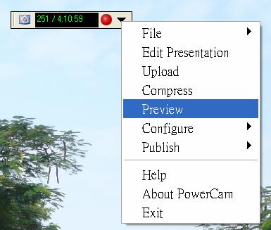
5 網路講義檔案兩種 :.pdf 一般講義檔只有文字說明.pcm 有聲動態講義檔有文字及語音說明對象 1. 課本閱讀困難 2. 上課無法充分理解 3. 自習用 可由 PowerCam 軟體讀取 PowerCam 可由學校義守大學 > 電算中心 > 電 算中心首頁 > 校內授權軟體 安裝 或由 powercam.com.tw/ 安裝 5
6 如何使用 PowerCam 請參考下步驟 Step 1 Step 2 6

7 Step 1 7
8 Step 2 8
9 9
10 教材左上符號 * Supplementary pages for illustration use. 補充教材 ~ The subject will not be covered in our current lecture. 目前略去 Examples in the Chapter will only be discussed on the class. 10
11 Chapter Four MOS Field-Effect Transistors (MOSFETs) 金氧半場效應電晶体 11
12 Introduction Three-terminal devices are far more useful than two- terminal ones. 三端子裝置比二端子裝置用途更多 The basic principle involved is the use of the voltage between two terminals to control the current flowing in the third terminal. 基本原理使用兩端電壓, 來控制第三端電流 There are two major types of three-terminal terminal semiconductor devices: the metal-oxide oxidesemiconductor field-effect effect transistor (MOSFET), which is study in this Chapter, and the bipolar junction transistor (BJT), which we shall study in Chapter 5. 三端子半導體半導體裝置有二主要型式 : 本章討論, 金氧半場效應電晶体 (MOSFET) 雙載子接面電晶体 (BJT), 則於下章討論 12
13 Compared to BJTs, MOSFETs can be made quite small (i.e., requiring a small area on the silicon IC chip), and their manufacture process is relatively simple. Also, their operation requires comparatively little power. 與 BJT 相較,MOSFET, 可做得更小 ( 需要更小矽 IC 晶元面積 ),, 製程簡單 同時, 使用更小功率 Furthermore, circuit designers have found ways to implement digital and analog functions utilizing MOSFETs almost exclusively (i.e., with very few or no resistors). 更而, 電路設計者可僅利用 MOSFET, 來實作數位及類比功能 ( 應用極少或不用電阻 ) 13
14 4.1 Device structure and physical operation 裝置結構及物理工作原理 The enhancement-type type MOSFET is the most widely used field-effect effect transistor. 在場效應電晶体, 加強型 MOSFET 為最常用 14
15 4.1.1 Device structure 裝置結構 Fig. 4.1 shows the physical structure of the n-channel enhancement-type type MOSFET. 圖 4.1 所示為 n 通道加強型 MOSFET 的物理結構 15
16 Figure 4.1 Physical structure of the enhancement-type NMOS transistor: (a) perspective view ( 透視圖 ); (b) cross-section ( 截面圖 ). Typically L = 0.1 to 3 μm, W = 0.2 to 100 μm, and the thickness of the oxide layer (t ox ) is in the range of 2 to 50 nm. 16
17 The transistor is fabricated on a p-type p substrate, which is a single-crystal silicon wafer that provide physical support for the device (and the entire circuit in the case of an integrated circuit). 電晶体為製於 p 型基體, 其為單晶矽晶片, 用來物理物理支撐裝置 ( 在積體電路時, 則為整個電路 ) Two heavily doped n-type n regions, indicated in the figure as the n + source and n + drain regions, are created in the substrate. 兩高濃度濃度參雜 n 區, 圖中的 n + 源極及 n + 汲極, 則製於基體上 A thin layer of silicon oxide (SiO 2 ) of thickness t ox (typically 2-50 nm), which is an excellent electrical insulator, is grown on the surface of the substrate, covering the area between the source and drain regions. 一極佳電絕緣極佳電絕緣薄層二氧化矽 (SiO 2 ), 厚度 t ox ( 典型 2-50 nm), 則長在基體表面, 涵蓋整個整個源極及汲極區空間源極及汲極區空間面積面積 17
18 Metal is deposited on top of the oxide layer to form the gate electrode of the device. In fact, most modern MOSFETs are fabricated using a process known as silicon-gate technology, in which a certain type of silicon, called polysilicon,, is used to form the gate electrode. 金屬沉積在氧化層頂上, 形成裝置的閘極 實際先進 MOSFET 製程為使用矽閘技術, 此時以多晶矽來形成閘電極 Metal contacts are also made to the source region, the drain region, and the substrate, also known as body. In actual IC, contact to the body is made at a location on the top of the device. 源極 汲極及基體 ( 亦稱母體 ) 製作金屬接點 實際 IC, 母體接點位置為在裝置頂層 18
19 Thus four terminals are brought out: the gate terminal (G), the source terminal (S), the drain terminal (D), and the substrate or body terminal (B). 接出四端子為 : 閘極閘 (G), 源極 (S), 汲極 (D) 及基體或母體 (B) At this point it should be clear that the name of the device (metal-oxide oxide-semiconductor FET) is derived from its physical structure. 金氧半場效應電晶体之名稱由此物理結構而得 19
20 + The notation n indicates heavily doped n-type silicon. Conversely, n is used to denote lightly doped n-type silicon. Similar notation applies for p-type silicon. 9 A nanometer (nm) ( ) is 10 m or 0.00 奈米 1 μm. 6 A micrometer ( μm) ( ), or micron, is 10 m. 微米 0.9 μm (or 900 nm) to 0.1 μm (or 100 nm) is submicron ( 次微米 ). Under 100 nm is deep submicron ( 深次微米 ) Sometimes the oxide thickness is expressed in angstroms. o 1 10 An angstrom ( A ) is 10 nm, or 10 m. 20
21 4.1.2 Operation with no gate voltage 沒閘極電壓時的操作 With no bias voltage applied to the gate, two back-to to-back diodes exist in series between drain and source. 當閘極沒偏電壓電壓加上加上時時, 在源極及汲極間為兩背對背二極體 These two back-to to-back diodes prevent current conduction from drain to source when a voltage v DS is applied. In fact, the path between drain and source has a very high resistance (of the order of Ω). 此兩背對背二極體, 使在加上 v DS 電壓下, 汲極至源極電流無法導通 實際上, 此間可看成存有一極高電阻 ( 次方達 Ω) 21

22 4.1.3 Creating a channel for current flow 造成通道使電流流動 Consider the situation depicted in Fig Here we have grounded the source and the drain and applied a positive voltage to the gate. 於圖 4.2 情況, 此處源極及汲極汲極接地, 而閘極加正電壓 22
23 The value of v GS at which a sufficient number of mobile electrons accumulate in the channel region to form a conducting channel is called the threshold voltage and is denoted V t. 當 v GS 上升至某值, 使足夠數目可動電子累積在通道區使, 而形一導電導電通道, 此電壓值稱門檻電壓, 以符號 V t 表示 V t for an n-channel n FET is positive. n 通道 FET, V t 為正 The value of V t is controlled during device fabrication and typically lies in the range of 0.5 V to 1.0 V. V t 值可於裝置製造時控制 典型為 0.5 V 至 1.0 V 23

24 4.1.4 Applying a small vds 加一小 vds We now apply a positive voltage v DS between drain and source, as shown in Fig
25 The conductance of the channel is proportional to the excess gate voltage (v V ), also known as the effective voltage or overdrive voltage. GS t Increasing v above the threshold voltage V GS enhances the channel, hence we name it enhancement-mode operation and enhancement-type MOSFET. t 25
26 Fig. 4.4 shows a sketch of i D versus v DS for various values of v GS. 26
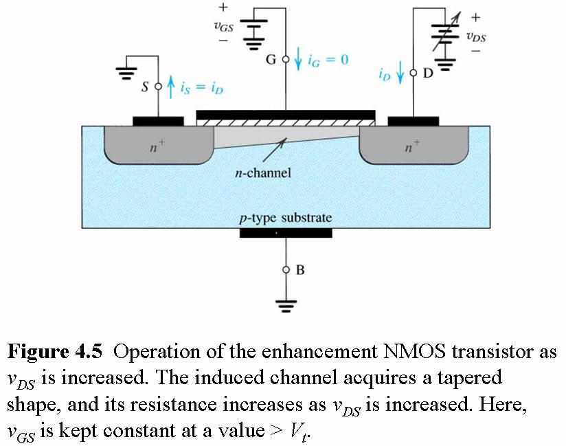
27 4.1.5 Operation as v DS 當 vds 增加 增加時的操作 increased DS For this purpose let v GS be held constant at a value greater than V t. 此時 v GS 值保持大於 V t Refer to Fig. 4.5, and note that v DS appears as a voltage drop across the length of the channel. 參看圖 4.5 注意, 此 v DS 為沿通道電壓降 27
28 The voltage between the gate and points along the channel decreases from v GS at the source end to v GS -v DS at the drain end. 閘與通道各點電壓, 從於源極端為 v GS, 沿途下降沿至汲極端為 v GS -v DS 28
29 29
30 Since the channel depth depends on this voltage, we find that the channel is no long of uniform depth; rather, the channel will take the tapered form shown in Fig. 4.5, being deepest at the source end and shallowest at the drain end. 因通道深度與此電壓有關, 故而通道深度深度將非均一, 而呈現逐漸變小, 如圖 4.5 在源極最深, 而汲極最淺 As v DS is increased, the channel becomes more tapered and its resistance increases correspondingly. 當 v DS 增加, 通道變得更尖細, 電阻對應亦增加 30

31 Thus the i D -v DS curve does not continue as a straight line but bends as shown in Fig 故而 i D -v DS 曲線不繼續呈現直線狀, 如圖 4.6 呈彎曲 See Fig. 4.4 Figure 4.6 The drain current i D versus the drain-to-source voltage v DS for an enhancementtype NMOS transistor operated with v GS > V t. 31
32 See Fig. 4.4 Figure 4.6 The drain current i D versus the drain-to-source voltage v DS for an enhancementtype NMOS transistor operated with v GS > V t. 32
33 Eventually, when v is increased to the value that GD t t DS the voltage between gate and channel at the drain end to V, that is, V = V or v v = V or v = v V GS DS t DS GS t the channel depth at the drain end decreases to almost zero, and the channel is said to be pinched off. 33
34 Increasing v beyond this value has little effect DS (theoretically, no effect) on the channel shape, and the current through the channel remains constant at the value reached for v = v V DS GS t. The drain current thus saturates at this value, and the MOSFET is said to have entered the saturation region of operation. Where v = v V DSsat GS t. 34
35 Obviously, for every value of v V, there is a corresponding value of v. The device operates in the saturation region if v DS v DSsat DSsat. GS t The region of the id v DS characteristic obtained for vds < vdss at is called the triode region. To help in visulizing the effect of v, we show in Fig. 4.7 sketches of the channel as v is increased GS DS while v is kept constant. DS 35
36 Figure 4.7 Increasing v DS causes the channel to acquire a tapered shape. Eventually, as v DS reaches v GS V t the channel is pinched off at the drain end. Increasing v DS above v GS V t has little effect (theoretically, no effect) on the channel s shape. 36
37 4.1.6 Derivation of the i D -v DS relationship 37

38 Figure 4.8 Derivation of the i D v DS characteristic of the NMOS transistor. 38
39 C ox = ε t ox ox : Capacitor formed by dielectric of oxide layer. where ε =3.9 ε is the permitivity of the silicon oxide, t ox 0 ox is the thickness of the oxide. μ n is the mobility of electrons in the channel. They are physical parameter whose value depends on the fabrication process technology. 39
40 The i-v relationship can be expressed as; W 1 2 In triode region, id = ( μncox) ( vgs Vt) vds 2 v DS, or L ' W 1 2 id = kn ( vgs Vt) vds 2 vds (4.5 a) L with k = μ C ' n n ox. In saturation region, where v v V, DS GS t 1 W 2 then id = 2 ( μncox) ( vgs V t), or L 1 ' W 2 id = 2 kn ( vgs Vt) (4.5 b) L with k = μ C ' n n ox 40
41 In the above equations, ' 2 n n ox μ C is a process transconductance parameters is denoted as k = μ C (A/V ). n ox and W/L is known as the aspect ratio of the MOSFET. transconductance: 跨導 aspect ratio: 縱橫比 41
42 Example 4.1 (p.245) (Considering a process technology, find its parameters and current, voltage.) 42
43 4.1.7 The p-channel p MOSFET A p-channel p enhancement-type type MOSFET (PMOS transistor), fabricated on an n-type n substrate with p + regions for the drain and source, has holes as charge carriers. The device operates in the same manner as the n-channel device except that v GS and v DS are negative and the threshold voltage V t is negative. Also, the current i D enters the source terminal and leaves through the drain terminal. Both PMOS and NMOS are utilized in complementary MOS or CMOS circuits, which is currently the dominant MOS technology. complementary: 互補式 43
44 4.1.8 Complementary MOS or CMOS Fig. 4.9 shows a cross-section section of a CMOS chip illustrating how the PMOS and NMOS transistors are fabricated. chip: 晶元 44
45 4.1.9 Operating the MOS transistor in the subthreshold region 工作於次門檻區的 MOS 電晶体 The above description of the n-channel n MOSFET operation implies that for v GS <V t, no current flows and the device is cutoff. This is not entirely true, for it has been found that for values of v GS smaller than but close to V t, a small drain current flows. In this subthreshold region of operation the drain current is exponentially related to v GS. 45
46 4.2 Current-voltage characteristics In this section we present the current- voltage characteristics of the enhancement MOS transistor. These characteristics can be measured at dc or at low frequencies and thus called static characteristics. 46
47 4.2.1 Circuit symbol Fig. 4.10(a) shows the circuit symbol for the n- n channel enhancement- type MOSFET. Figure 4.10 (a) Circuit symbol for the n- channel enhancement-type MOSFET. (b) Modified circuit symbol with an arrowhead on the source terminal to distinguish it from the drain and to indicate device polarity (i.e., n channel). (c) Simplified circuit symbol to be used when the source is connected to the body or when the effect of the body on device operation is unimportant. 47
48 4.2.2 The i D -v characteristics DS Fig. 4.11(a) shows an enhancemen t-type type MOSFET with voltages v GS and v DS applied and with the normal directions of current flow indicated. (a) An n-channel enhancement-type MOSFET with vgs and vds applied and with the normal directions of current flow indicated. 48
 indicate that there are three distinct regions of the operation: cutoff region, the triode region, and the saturation region.")
49 The characteristic curves in Fig. 4.11(b) indicate that there are three distinct regions of the operation: cutoff region, the triode region, and the saturation region. The saturation region is used if FET is used as an amplifier. For operation as a switch, the cutoff and triode regions are utilized. 49
50 Cutoff region ( (v GS <V ) t No enough carriers exist in the channel to form current. 50
51 Triode region (v( GS v DS > V t ) First, v GS V t (Induced channel) Then, v GD > V t (Continuos channel) In words, the n-channel n enhancement-type type MOSFET operates in the triode region when v GS is greater than V t and the drain voltage is lower than the gate voltage by at least V t volts. ' 1 2 id = k W n ( vgs Vt) vds 2 vds (4.11) L 51
52 ' 1 2 id = k W n ( vgs Vt) vds 2 vds (4.11) L If v is sufficiently small (v 2 V, where V =V V, DS DS OV OV GS t and the V is called gate-to-source overdrive voltage.), OV we can obtain a i -v characteristics near the origin in the form as i k ( v V ' W D n L GS t D ) v DS DS This linear relationship represents the operation of the MOS transistor as a linear resistance r whose value is controlled by v GS. DS 52
53 Saturation region (v( DS v GS -V t ) v GS V t (Induced channel) GD V t (Pinched-off channel) v GD In words, the n-channel n enhancement-type type MOSFET operates in the saturation region when v GS is greater than V t and the drain voltage does not fall below the gate voltage by more than V t volts. 53
54 Boundary between triode region and the saturation region is v DS = v GS V t In the saturation region, the drain current is i k v V 1 ' W 2 D = 2 n L ( GS t) (4.20) In saturation the MOSFET provides a drain current whose value is independent of the drain voltage v and is determined by the gate voltage v according the above square-law relationship, a sketch of which is shown in Fig GS DS 54
55 Figure 4.12 The i D v GS characteristic for an enhancement-type NMOS transistor in saturation (V t = 1 V, k n W/L = 1.0 ma/v 2 ). 55
56 Since the drain current is independent of drain voltage, the saturated MOSFET behaves as an ideal current source whose value is controlled by v according to the above nonlinear relationship. GS 56
57 Fig shows its circuit representation. This is a large-signal equivalent-circuit model. 57
) of an n-channel MOSFET operating in the saturation region. 58")
58 Figure 4.13 Large-signal equivalent-circuit model (Based on Eq. (4.20)) of an n-channel MOSFET operating in the saturation region. 58
59 The chart in Fig shows the relative levels of the terminal voltages of the enhancement-type type NMOS transistor for operation, both in the triode region and the saturation region. 59
60 Figure 4.14 The relative levels of the terminal voltages of the enhancement NMOS transistor for operation in the triode region and in the saturation region. 60
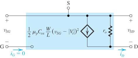
61 4.2.3 Finite output resistance in saturation 飽和區的有限輸出電阻 As v DS is increased, the channel pinch-off point is moved slightly away from the drain, toward the source. The channel length is effect reduced, from L to L ΔL, L L, a phenomenon known as channel-length length modulation. Since i D is inversely proportional to the channel length, i D increases with v DS. 61
.")
62 v v = V Pinch off (or v = v = v V GS DS t DS DSsat GS t ) v v < V Saturation ( or v > v V ) GS DS t DS GS t 1 ' W 2 id = 2 kn L ( vgs Vt) (4.20) Figure 4.15 Increasing v DS beyond v DSsat causes the channel pinch-off point to move slightly away from the drain, thus reducing the effective channel length (by ΔL). 62
63 By introducing a process-technology parameter λ with -1 the dimension of V and for a given process, is inversely proportional to the length selected for the channel. In terms of λ, the expression for i becomes W i k v V v L 1 ' 2 D = 2 n ( GS t) (1 + λ DS) D λ The above equation indicates that i =0 and v = 1/ λ. D DS 63
64 It follows that V A = 1/ λ and thus V A is a process-technology parameter with the dimensions of V. For a given prcess, V A is proportional to the channel length L that designer selects for a MOSFET. 64
65 Fig shows a typical i -v characteristics with the effect of channel-length modulation. D DS 65
66 Just as in the case of λ, we can isolate the dependence of V on L by expressing it as V A = V L ' A A where V is entirely process-technology dependent with the ' A dimension of V/ μm. Typically, V falls in the range of 5 V/ μm to 50 V/ μm. ' A The voltage V is usually referred to as the Early voltage. A Early voltage: 爾利電壓 66
67 Defining the output resistance as r o i 1 D = vds v = constant GS and using Eq. (4.22) results in ' kn W ro = λ ( VGS Vt) 2 L 2 1 which can be written as r o 1 V = = λi I D A D 67
68 For r o = V I A D (4.26) I is the current without channel length modulation taken D into account; that is, 1 W I = k ( V V ) 2 L ' 2 D n GS t Thus the output resistance is inversely proportional to the drain current. 68
69 Fig shows the large-signal equivalent circuit model incorporating r o. 69
.")
70 Figure 4.17 Large-signal equivalent circuit model of the n- channel MOSFET in saturation, incorporating the output resistance r o. The output resistance models the linear dependence of i D on v DS and is given by Eq. (4.22). For p-channel MOSFET the model is different (see page 262). 70
71 4.2.4 Characteristics of the p-channel p MOSFET The circuit symbol for the p-channel p enhancement-type type MOSFET is shown in Fig. 4.18(a). Fig. 4.18(b) shows a modified circuit symbol in which an arrowhead pointing in the normal direction of current flow is included on the source terminal. 71
72 Figure 4.18 (d) The p-channel MOSFET with voltages applied and the directions of current flow indicated. Note that v GS and v DS are negative and i D flows out of the drain terminal. 72
73 Figure 4.19 The relative levels of the terminal voltages of the enhancement-type PMOS transistor for operation in the triode region and in the saturation region. 73
74 4.2.5 The role of the substrate The body effect 基體的角色 -- 母體效應 In many applications the source terminal is connected to the substrate (or body) terminal B, which results in the pn junction between the substrate and the induced channel (see Fig. 4.5) having a constant zero (cutoff) bias. Fig
75 In such a case the substrate does not play any role in circuit operation and its existence can be ignored altogether. 75
76 In integrated circuits, however, the substrate is usually common to many MOS transistors. In order to maintain the cutoff condition for all the substrate-to to-channel junctions, the substrate is usually connected to the most negative power supply in an NMOS circuit (or the most positive in the PMOS circuit). The resulting reverse-bias voltage between source and body (V SB in an n-channel n device) will have an effect on device operation. 76
77 The effect of V on the channel can be most conveniently SB represented as a change in the threshold voltage V Specifically, it has been shown that increasing the reverse substrate bias voltage V SB results in an increase in V t according to the relationship Vt = Vto + γ 2φf + VSB 2 φ f (4.33) t. where V is the threshold voltage for V = 0; φ is a t0 SB f physical paremeter with ( 2 φ ) typically 0.6V; f V = V, as V SB BS BS increases the V t will decrease. 77
78 Where γ is a fabrication-process parameter given by γ = 2qN C ox A ε s where q is the electron charge, N in the doping concentration of the p-type substrate, of silicon. A ε is the permittivity s The parameter 1/2 γ has dimension of V and typically 0.4 V. 78
79 Equation (4.33) indicates that an incremental change in V SB gives rise to an incremental change in V t, which in turn results in a change in i D even though v GS might have been kept constant. (See the following current relationship) = 1 ' W ( ) 2 D 2 n L GS t i k v V It follows that the body voltage controls i D ; thus the body acts as another gate for the MOSFET, a phenomenon known as the body effect. Here we note that the parameter γ is known as the body-effect parameter. 79
80 4.2.6 Temperature effects Both V t and k' k are temperature sensitive. (See the following equation for k' ) W W = = L L ' ' k ( μ ncox) kn 80
81 4.2.7 Breakdown and Input protection Avalanche breakdown It occurs at pn junction between drain region and substrate. The voltage is around 20 to 150 V and results in a somewhat rapid increase in current (known as a weak avalanche). Punch-through For short channel when the drain voltage is increased to the point that the depletion region surrounding the drain region extends through the channel to the source. The drain current then increases rapidly. It occurs at lower voltage (about 20V) in modern devices. Normally, it does not result in permanent damage to the device. 81
82 Input protection: Another kind of breakdown occurs when the gate-to to- source voltage exceeds about 30V. This is the breakdown of gate oxide and results in permanent damage to the device. It must be remembered that MOSFET has a very high input resistance, and a very small input capacitance, thus small amounts of static charge accumulating on the gate capacitor can cause its breakdown voltage to be exceeded. To prevent this breakdown, gate-protection devices, such as clamping diodes, are usually included at the input terminals of MOS integrated circuits. clamping diode: 鉗制二極體 82
83 4.2.8 Summary Table

84 Table
85 85
86 4.3 MOSFET circuits at DC Having studied the current-voltage characteristics of MOSFETs,, we now consider circuits in which only dc voltages and currents are of concern. 86
87 Example 4.2 (p.263) The NMOS transistor operates at I =0.4 ma and V =+0.5 V. It has V V μ C μa V L 1 μm, and W μm. 2 t = 0.7, n ox = 100 /, = = 32 Neglect the channel-length modulation effect. Find R, R? D D S D 87
88 Figure 4.20 Circuit for Example
89 Example 4.3 (p.264) 89
90 Figure 4.21 Circuit for Example
91 91
92 Example 4.4 (p.265) 92
93 Figure 4.22 Circuit for Example
94 Example 4.5 (p.266) 94
95 Figure 4.23 (a) Circuit for Example 4.5. (b) The circuit with some of the analysis details shown. 95
96 Example 4.6 (p.268) 96
97 Figure 4.24 Circuit for Example
98 Example 4.7 (p.269) 98
99 Figure 4.25 Circuits for Example
100 4.4 The MOSFET as an amplifier and as a switch In this section we study the use of MOSFETs in the design of amplifier circuits. The basis for this important MOSFET application is that when operated in the saturation region, the MOSFET acts as a voltage-controlled current source: Changes in the gate-to to-source voltage v GS give rise to changes in the drain current i D. Thus the saturated MOSFET can be used to implement a transconductance amplifier (see p.28, Section 1.5). 100
 輸入電壓, 輸出電流 模型含增益 G m")
101 Repeat of Chapter One, p28 Transconductance amplifier ( 跨導或互導 放大器 ) 輸入電壓, 輸出電流 模型含增益 G m 的電壓控制電流源 101
102 The technique we will utilize to obtain linear amplification from a fundamentally nonlinear device is that of dc biasing the MOSFET to operate at a certain appropriate V GS and a corresponding I D and then superimposing the voltage signal to be amplified, v gs, on the dc bias voltage V GS. 利用基本非線性裝置來取得線性放大的技術, 為 MOSFET dc 偏位的操作的操作 此為, 以某適當以 V GS 及對應 I D, 於 dc 偏壓 V GS 上加所要放大信號電壓 v gs By keeping the signal v gs small, small, the resulting change in the drain current i d, can be made proportional to v gs. 在保持小信號 v gs 下, 則可做到汲極電流 i d 與 v gs 成正比 102
103 Before considering the small-signal signal operation of the MOSFET amplifier, we will look at the big picture : : We will study the total or large-signal operation of MOSFET amplifier. 於討論 MOSFET 放大器小信號操作小信號操作前, 先了解 MOSFET 放大器的大信號操作 From the voltage transfer characteristic we will be able to clearly see the region over which the transistor can be biased to operate as a small- signal amplifier as well as those region where it can be operated as a switch (i.e., being either fully on or fully off ). 103
104 4.4.1 Large-signal operation The transfer characteristic 大信號操作 -- 轉移特性 Fig. 4.26(a) shows the basic structure of the most commonly used MOSFET amplifier, the common-source (CS) circuit. 圖 4.26a 所示為最通用 MOSFET 放大器的基本架構 此為一共源極 (CS) 電路 104
105 The name common-source or ground- source circuit arises because when the circuit is viewed as a two-port network, the grounded source terminal is common to both the input port, between gate and source, and the output port, between drain and source. 105
106 Note that although the basic control action of the MOSFET is that changes in v (here, changes in v as v = v ) give rise to changes in i output voltage v v O, GS I GS I D O = vd S = V DD R D i D, we are using a resistor R to obtain an D In this way the transconductance amplifier is converted into avoltage amplifier. Note that a dc power supply is needed to turn the MOSFET on and to supply the necessary power for its operation. 106
107 We wish to analyze the circuit of Fig. 4.26(a) to determine its output voltage v for various values of input voltage v, O that is, to determine the voltage transfer characteristic of the CS amplifier. I For this purpose, we will assume v to be in the range of 0 to V. DD I Voltage transfer characteristic: 電壓轉移特性 107
108 To obtain greater insight into the operation of the circuit, we will derive its transfer characteristic in two ways: graphically and analytically. 108
109 4.4.2 Graphical derivation of the transfer characteristic 轉移特性的圖形導法 The operation of the common-source cicruit is governed by the MOSFET's i v characteristics and by the D D DS relationship between i and v imposed by connecting the drain to the power supply V via resistor R, namely v = V R i DS DD D D DS DD D or equivalently, i D V R DD = D 1 R D v DS (4.37) 109
110 Fig 4.26(b) shows a sketch of the MOSFET's i v. D DS characteristic curve superimposed on which is a straight line representing i v relationship of Eq. (4.37). d DS Figure 4.26 (b) Graphical construction to determine the transfer characteristic of the amplifier in (a). 110
111 Observe that the straight line intersects the v axis at V and has a slope of D D DS DD 1/ R. Since R is usually thought of as the load resistor of the amplifier (i.e., the resistor across which the amplifier provides its output voltage), the straight line in Fig. 4.26(b) is known as the load line. 111
112 The point-by bypoint determination of the transfer characteristic results in the transfer curve shown in Fig. 4.26(c). We have delineated its three distinct segments, each corresponding to one of the three regions of operation of MOSFET Q 1 in Fig. 4.26(b). 112
113 Point X to A Figure 4.26 (b) Graphical construction to determine the transfer characteristic of the amplifier in (a). 113
114 4.4.3 Operation as a switch When the MOSFET is used as a switch, it is operated at the extreme points of the transfer curve. On the segment of XA, the device is turned off: v < V and v = V I t O DD At C the device is turned on: v = V and v = V I DD O OC 114
115 The common-source MOSFET circuit can be used as a logic inverter with the low voltage level close to 0 V and the high voltage level close to V DD. logic inverter: 邏輯反相器 115
116 4.4.4 Operation as a linear amplifier To operate the MOSFET as an amplifier we make use of the saturation-mode segment of the transfer curve. The device is biased at a point located somewhere close to the middle of the curve; point Q is an example of an appropriate bias point. 116
117 Figure 4.26 (c) Transfer characteristic showing operation as an amplifier biased at point Q. 117
118 This dc bias point is also called the quiescent point,, which is the reason for labeling it Q. The voltage signal to be amplified v i is then superimposed on the dc voltage V IQ as shown in Fig. 4.26(c). 118
119 Figure 4.26 (c) Transfer characteristic showing operation as an amplifier biased at point Q. 119
120 By keeping v i sufficiently small to restrict operation to an almost linear segment of the transfer curve, the resulting output voltage signal v o will be proportional to v i. 120
121 That is, the amplifier will be very nearly linear, and v o will have the same waveform as v i except that it will be larger by a factor equal to the voltage gain of the amplifier at Q, A v, where A v = dv dv O I v = V I IQ Thus the voltage gain is equal to the slope of the transfer curve at the bias point Q. The slope is negative, and thus the basic CS amplifier has a negative voltage gain A. v 121
122 It is important to note that although we make the selection of bias-point location of a given transfer curve, the circuit designer also has to decide on a value for R D, which determines the transfer curve. It is more appropriate when considering the location of the bias point Q we refer to the i D -v DS plane. This is illustrated by the sketch in Fig
123 Different load lines for different R D values: Figure 4.27 Two load lines and corresponding bias points. Bias point Q 1 does not leave sufficient room for positive signal swing at the drain (too close to V DD ). Bias point Q 2 is too close to the boundary of the triode region and might not allow for sufficient negative signal swing. 123
124 4.4.5 Analytical expressions for the transfer characteristic 轉移特性的解析表示 The i-v relationships that describe the MOSFET operation in the three regions cutoff, saturation, and triode can be used to derive analytical expressions for the three segments of the transfer characteristic in Fig. 4.26(c). 124
125 Figure 4.26 (c) Transfer characteristic showing operation as an amplifier biased at point Q. 125
126 (See p.275~277 for detail) The cutoff-region segment, XA: Here, v V, and v =V. O I DD t The saturation-region segment, AQB: Here, v V, I and v v -V. O I t t The triode-region segment, BC: Here, v V, I and v v -V. O I t t 126
127 Example 4.8 (p.277) (to make the above analysis more concrete we consider a numerical example. In Fig. 4.26(a)..) 127
128 Figure 4.26 (a) Basic structure of the common-source amplifier. 128
129 Figure 4.28 Example
130 Figure 4.28 (Continued) 130
131 4.4.6 A final remark on biasing To generate a constant bias voltage by using a fixed value of v GS is not a good method. We will explain why this is so in the next section. 131
132 4.5 Biasing in MOS amplifier circuits An essential step in the design of a MOSFET amplifier circuit is the establishment of an appropriate dc operating point for the transistor. An appropriate dc operating point or bias point is characterized by a stable and predictable dc drain current I D and by a dc drain-to to-source voltage V DS that ensures operation in the saturation region for all expected input-signal levels. 合適的 dc 工作點或偏位點特徵為 : 第一, 穩定及可預期的汲極電流 I D 第二, 汲極至源極電壓 V DS 可保證在預期所要所要輸入信號水準下, 電晶体工作於飽和區 132
133 4.5.1 Biasing by fixing V GS To emphasize the point that biasing by fixing V GS is not a good technique, we show in the Fig two i D -v GS characteristic curves representing extreme values in a batch of MOSFETs of the same type. 133
134 Figure 4.29 The use of fixed bias (constant V GS ) can result in a large variability in the value of I D. Devices 1 and 2 represent extremes among units of the same type. 134
135 Observe that for the fixed value of V GS, the resultant spread in the values of the drain current can be substantial. 135
136 4.5.2 Biasing by fixing V G and connecting a resistance in the source Figure 4.30 Biasing using a fixed voltage at the gate, V G, and a resistance in the source lead, R S : (a) basic arrangement; 136
137 For the circuit we can write V = V + R I G GS S D or I D V GS = + R S V R G S where V G / R can be considered as a constant. S The resistor R gives rise to a negative feedback S action. It is called a degeneration resistance. Degeneration resistance: 退化電阻 137
138 138
139 Fig. 4.30(b) provides a graphical illustration of the effectiveness of this bias scheme. Figure 4.30 Biasing using a fixed voltage at the gate, V G, and a resistance in the source lead, R S : (b) reduced variability in I D ; (c) practical implementation using a single supply; 139
140 Figure 4.30 Biasing using a fixed voltage at the gate, V G, and a resistance in the source lead, R S : (d) coupling of a signal source to the gate using a capacitor C C1 ; (e) practical implementation using two supplies. 140
141 Example 4.9 (p.283) It is required to design the circuit of Fig. 4.30(c) to establish 141
142 Figure 4.31 Circuit for Example
143 4.5.3 Biasing using a drain-to to-gate feedback resistor 使用汲極至閘極負回授電阻的偏位 A simple and effective discrete-circuit circuit biasing arrangement utilizing a feedback resistor connected between the drain and the gate is shown in Fig
144 Figure 4.32 Biasing the MOSFET using a large drainto-gate feedback resistance, R G. 144
145 Here the large feedback resistance R G (usually in the MΩM range) forces the dc voltage at the gate to be equal to that at the drain (because I G =0). 145
146 V = V = V R I GS DS DD D D If I for some reason changes, say increases, then V D must decreases. This decrease in V in turn causes a decrease in I, a change that is opposite in direction with one originally D assumed. This is a negative feedback. GS GS The circuit can be utilized as a CS amplifier by applying the input voltage signal to the gate and take drain output via capacitors so as not to disturb the dc bias conditions. The drawback of this circuit is a rather limited output voltage signal swing. 146
147 4.5.4 Biasing using a constant-current current source The most effective scheme for biasing a MOSFET amplifier is that using a constant- current source. Fig. 4.33(a) shows such an arrangement applied to a discrete MOSFET. 147
148 Figure 4.33 (a) Biasing the MOSFET using a constant-current source I. 148
149 A circuit for implementing the constant-current source I is shown in Fig. 4.33(b). (See Fig for degeneration effect) Where we have neglected channel-length modulation and assume that they are operated in the saturation regions. 149
150 Figure 4.33 (b) Implementation of the constant-current source I using a current mirror. 150
151 The drain current in Q is W I = k ( V V ) 1 ' 2 D1 2 n GS t L 1 1 Since the gate currents are zero, I D1 = I = REF V + V V DD SS GS R Now consider transistor Q W I = I = k ( V V ) 1 ' 2 D2 2 n GS t L 2 2 : 151
152 Thus we can express the relationship of I and I as I = I REF ( W / L) ( W / L) 2 1 REF This circuit, known as a current mirrow, is very popular in the design of IC MOS amplifier. 152
153 4.5.5 A final remark The bias circuits studied in this section are intended for discrete-circuit circuit applications. The only exception is the current mirror circuit which is extensively used in IC design. 153
154 4.6 Small-signal operation and models We use the common-source amplifier circuit shown in Fig for the analysis. 154
155 Figure 4.34 Conceptual circuit utilized to study the operation of the MOSFET as a small-signal amplifier. 155
156 4.6.1 The DC bias point The dc bias current I can be found by setting the signal v to zero; thus, gs I = 2 k ( V V ) 1 ' W 2 D n L GS t D where we have neglected the channel-length modulation. 156
157 The dc voltage at the drain, V or simply V, will be V = V R I D DD D D DS D To ensure saturation-region operation, we must have V > V V D GS t Furthermore, since the total voltage at the drain will have a signal component superimposed on V, V has to be sufficiently greater than (V (see Fig. 4.14). GS D V ) to allow for the required signal swing t D 157
158 Figure 4.14 The relative levels of the terminal voltages of the enhancement NMOS transistor for operation in the triode region and in the saturation region. 158
159 4.6.2 The signal current in the drain terminal Next, consider the situation with the input signal v gs applied. 159
160 With v = V + v GS GS gs The resulting total drain current is i = k ( v V ) 1 ' W 2 D 2 n L GS t = k ( V + v V ) 1 2 ' W 2 n L GS gs t = k ( V V ) + k ( V V ) v + k v 1 ' W 2 ' W 1 ' W 2 2 n L GS t n L GS t gs 2 n L gs The last component represents a nonlinear distortion and is an undesirable term. 160
161 By keeping the input signal small, 1 2 k v << k ( V V ) v ' W 2 ' W n L gs n L GS t gs Or equivalently, v << 2( V V ) gs GS t Under this small signal condition, i can be expressed as i I + i D D d D where i = k ( V V ) v. ' W d n L GS t gs 161
162 The parameter that relates i and v is the MOSFET transconductance g m, i g = = k ( V V ) = k V (4.61) d ' W ' W m n L GS t n L OV vgs d gs Fig present a graphical interpretation of the small-signal operation of the enhancement MOSFET amplifier. It is equal to the slope of the i v characteristic at the bias point, g m i = D v GS v = V GS GS D GS 162
163 Figure 4.35 Small-signal operation of the enhancement MOSFET amplifier. 163
164 It is equal to the slope of the i v characteristic at the bias point, g m i = D v GS v = V GS GS D GS 164
165 4.6.3 The voltage gain In Fig. 4.34, we can express the total instantaneous drain voltage v as follows: D v = V R i D DD D D 165
166 Under the small-signal condition, we have v = V R (I + i ) D DD D D d Or v = V R i = V + v D D D d D d Thus the signal component of the drain voltage is v = R i = R ( g v ) = g R v d D d D m gs m D gs Which indicates that the voltage gain is given v v d gs = g R m D by 166
167 Fig shows v GS and v D. 167
168 Figure 4.36 Total instantaneous voltages v GS and v D for the circuit in Fig
169 Output signal v d is 180 out of phase with respect to the input signal v gs. 169
170 Figure 4.36 Total instantaneous voltages v GS and v D for the circuit in Fig
171 Input signal is assumed to have a triangular waveform with an amplitude much smaller than 2(V GS V t ). To ensure all operation within the saturation, the minimum value of v D should not fall below the corresponding value of v G by more than V t (with inverse phase case, v Gmax -V t ). Also, the maximum value of v D should be smaller than V DD. 171
172 Figure 4.36 Total instantaneous voltages v GS and v D for the circuit in Fig
173 4.6.4 Separating the DC analysis and the signal analysis Under the small-signal signal approximation, signal quantities are superimposed on dc quantities. The analysis and design can be greatly simplified by separating dc or bias calculations from small-signal signal calculations. That is, once a stable dc operating point has been established and all dc quantities calculated, we may then perform signal analysis ignoring dc quantities. 173
174 174
175 For instant, the total drain current i D equals the dc current I D plus the signal current i d, the total drain voltage v D = V D + v d. In the analysis and design, we can separate the dc or bias calculations from small-signal signal calculations. 175
176 176
177 4.6.5 Small-signal equivalent-circuit models From a signal point of view the FET behaves as a voltage-controlled current source. Fig. 4.37(a) represents its small-signal signal operation and is a small-signal signal model or a small-signal signal equivalent circuit. 177
178 Figure 4.37 Small-signal models for the MOSFET: (a) neglecting the dependence of i D on v DS in saturation (the channel-length modulation effect); and (b) including the effect of channel-length modulation, modeled by output resistance r o = V A /I D (see p.255). Typically, r o is in the range of 10 kω to 1000 kω. 178
179 The output resistance that is, the resistance r o looking into the drain is high, and we have assumed it to be infinite. 179
180 In the analysis of a MOSFET amplifier circuit, the transistor can be replaced by the equivalent circuit model. This model is referred to as the hybrid-π model, a carryover from the bipolar transistor literature. The rest of circuit remains unchanged except the ideal constant dc voltage sources are replaced by short circuits. This is a result of the fact that the voltage across an ideal constant dc voltage source does not change, and thus there will always be zero voltage signal across a constant dc voltage source. 180
181 A dual statement applies for constant dc current source; namely, the signal current of an ideal constant dc current source will always be zero, and thus an ideal dc constant current source can be replaced by an open-circuit in the small- signal equivalent circuit of the amplifier. 181
182 From our study of the MOSFET characteristics in saturation, we know that the drain current does in fact depends on v DS in a linear manner. This is the effect of channel-length length modulation. Such a dependence was modeled by a finite resistance r o between drain and source, as shown in Fig. 4.37(b). 182
183 Figure 4.37 Small-signal models for the MOSFET: (a) neglecting the dependence of i D on v DS in saturation (the channel-length modulation effect); and (b) including the effect of channel-length modulation, modeled by output resistance r o = V A /I D (see p.255). Typically, r o is in the range of 10 kω to 1000 kω. 183
184 Where r o = and V I A D W I = k V L 1 ' 2 D 2 n OV The voltage gain can be expressed as vd Av = = gm( RD // ro) v gs 184
185 4.6.6 The transconductance g m By Eq. 4.61, the transconductance of an MOSFET is g = k ( W / L)( V V ) = k ( W / L) V (4.69) ' ' m n GS t n OV 185
186 Another expression can be obtained by substituting for 2I D ( VGS V t ) with. k ( W / L) That is, ' n ' m = 2 n / D (4.70) g k W L I Yet, another expression is g m 2ID ID ID = = = V V ( V V )/2 V /2 GS t GS t OV (4.71) 186
187 In summary, there are three different relationships for determining g -- Eqs. (4.69), (4.70), and (4.71). m There are three design parameters -- (W/L), V, and I, any two of which can be chosen independently. OV D That is, the designer may choose to operate the MOSFET with a certain overdrive voltage V and a particular current I ; the required W/L ratio can then be found and the resulting D g determined. m OV 187
188 The values of g m : For a device operating at ' 2 I D = 0.5 ma and having kn = 120 μ A/ V, with W/L= 1, then g = 0.35 ma/ V. m For a device W/L = 100, then g = 3.5 ma / V. m (Comparing with BJT operating at a collector current of 0.5 ma, it has g m m = 20 ma/v. (g for BJT will be explained in Chapter 5) 188
189 Example 4.10 (p.293) (We wish to analyze the amplifier circuit to determine its small-signal signal voltage gain, its input resistance, and largest allowable input signal.) 189
190 Figure 4.38 Example 4.10: (a) amplifier circuit; 190
191 Figure 4.38 Example 4.10: (b) equivalent-circuit model. 191
192 4.6.7 The T equivalent-circuit model Through a simple circuit transformation it is possible to develop an alternative equivalent circuit model for the MOSFET. The development of such a model, known as the T model, is illustrated in Fig In order to distinguish the model of Fig. 4.37(b) from the equivalent T model, the former is sometimes referred to as the hybrid-πmodel. 192

193 Figure 4.39 Development of the T equivalent-circuit model for the MOSFET. For simplicity, r o has been omitted but can be added between D and S in the T model of (d). 193
 The T model of the MOSFET augmented with the drain-to-source")
194 Figure 4.40 (a) The T model of the MOSFET augmented with the drain-to-source resistance r o. (b) An alternative representation of the T model. 194
195 4.6.8 Modeling the body effect In integrated circuits, the substrate is usually common to many transistors. In order to maintain the cutoff condition for all the substrate-to to-channel junctions, the substrate is usually connected to the most negative power supply in an NMOS circuit (the most positive in a PMOS circuit). The resulting reverse-bias voltage between source and body (V SB in an n-channel n device) will have an effect on device operation. 195
196 The substrate acts as the "second gate" or a backgate for the MOSFET. The signal v gives rise to a drain-current component bs which we shall write as g v, where g is a body transconductance, defined as mb bs mb g mb i = D v BS vgs = constant v = constant DS 196
197 Recalling that i depends on v through the dependence t D of V, and for NMOS, increases v corresponds to increasing i, we can obtain g = χ g, where BS BS D mb m Vt γ χ = = V 2 2φ + V SB f SB Typical value for χ lies in the range 0.1 to

198 Figure 4.41 Small-signal equivalent-circuit model of a MOSFET in which the source is not connected to the body. (Note that the direction of voltage applied is from body-to-source) 198
199 4.6.9 Summary Table 4.2 Small-signal equivalent-circuit models for MOSFET 199

200 Table
201 4.7 Single-stage MOS amplifier In this section we study the case of discrete MOS amplifiers. The separation between dc and signal quantities is more obvious in discrete circuits, and discrete circuits utilizes resistors as amplifier loads. Since in discrete circuits the MOSFET source is usually tied to the substrate, the body effect will be absent. 201
202 4.7.1 The basic structure Fig shows the basic circuit we shall utilize to implement the various configurations of discrete-circuit circuit MOS amplifiers. 202
203 Figure 4.42 Basic structure of the circuit used to realize singlestage discrete-circuit MOS amplifier configurations. 203
204 4.7.2 Characterizing amplifier As we begin our study of MOS amplifier circuits, it is important to know how to characterize the performance of amplifiers as circuit building block. 在了解 MOS 放大器電路前, 首先要知道, 如何將放大器, 在當成電路構築方塊時, 性能特性化 204
205 Repeat here the four amplifier types defined in Table 1.1. (see p.28, Chapter 1). 205
206 An amplifier 206
207 Recapitulation from Table 1.1 Voltage amplifier Gain parameter Ideal Characteristics 207

208 Recapitulation from Table 1.1 Current amplifier Gain parameter Ideal Characteristics 208
209 Recapitulation from Table 1.1 Transconductance amplifier Gain parameter Ideal Characteristics 209

210 Recapitulation from Table 1.1 Transresistance amplifier Gain parameter Ideal Characteristics 210
211 The amplifier models considered In Table 1.1 are unilateral; that is, signal flow in unidirectional, from input to output. 表 1.1 所討論放大器為單側性, 即信號流向為由輸入到輸出 Most real amplifiers shows some reverse transmission, which is usually undesirable but must nonetheless be molded. 大部分實際放大器會呈現逆向傳輸, 此逆向傳輸一般並非所要, 但在模型上則需另考慮 211
212 A number of the amplifier circuits have internal feedback that may cause their input resistance to depend on the load resistance. Similarly, internal feedback may cause the output resistance to depend on the value of the resistance of the signal source feeding the amplifier. To accommodate nonunilateral amplifiers, we present, in Table 4.3, a general set of parameters and equivalent circuits that we will employ in characterizing and comparing transistor amplifiers. 為迎合非單側性放大器, 在表 4.3 為一般等效電路參數組 此可做為做為電晶体放大器特性化及比較用 212
213 Table 4.3 Characteristic parameters of amplifiers (p.302) Conceptual view of amplifier Circuit Signal source Amplifier load 213
214 Remark 1 The amplifier is shown fed with a signal source having an open-circuit voltage v and an internal resistance R sig sig. These can be the parameters of an actual signal source or the Thevenin equivalent of the output circuit of another amplifier stage preceding the one under study in a cascade amplifier. Similarly, R L can be an actual load resistance or the input resistance of a suceeding amplifier stage in a cascade amplifier. 214
215 R i Input resistance with no load (R L = ): R = i v i i i R = L 215
216 R in Input resistance: R in = v i i i (R can be any value from 0 to. When R =, R =R L L in i.) 216
217 R o Output resistance with v = 0: R = i o v x i x v = 0 i 217
218 R out Output resistance: v R = (When R =0, R =R.) x out sig out o i x v = 0 sig 218
219 A vo Open-circuit voltage gain: A vo = v v o i R L = This is the maximum voltage gain that an amplifier can provide. The A v represents Thevenin equivalent voltage at its output. vo i 219
220 A is Short-circuit current gain: A is = i i o i R L = 0 This is the maximum current gain that an amplifier can provide. 220
221 G m Short-circuit transconductance: G m = i o v i R = 0 L 221
222 A v Definitions including the effect of R : L Voltage gain: v = o A v (R L can be any value from 0 to, vi when R =0, A =0, and when R =, A = A.) L v L v vo 222
223 A i Definitions including the effect of R : L Current gain: i o A i = (R L can be any value from 0 to, ii when R =0, A=A, and when R =, A = 0.) L i is L i 223
224 G and G vo v Definitions including the effect of one or both of R and R : sig L Open-circuit overall voltage gain: v G = (v replaces with v in A. Note v = v o in vo sig i vo i sig vsig R R in + R = sig L R.) Overall voltage gain: G v = v v o sig (R can be any value from 0 to, when R =0, G =0, L L v and when R =, G = G.) L v vo 224
225 Remark 2 Parameters R, R, A, A, and G pertain to the i o vo is m amplifier proper; that is, values of R and R. sig L they do not depend on the By contrast, R, R one or both of, A, A, G, and G may depend on in out v i vo v R and R sig L. Some relationships of the related pairs are R = R, and R = R. i in R = o out R = 0 L sig 225
226 Remark 3 As mentioned above, for nonunilateral amplifiers, R in may depend on R L. And R out may depend on R sig. No such dependencies exist for unilateral amplifiers, for which R in = R i and R out = R o. 226
227 Remark 4 The loading of the amplifier on the signal source is determined by the input resistance R in The value of R in determines the current i i that the amplifier draws from the signal source. It also determines the proportion of the signal v sig that appears at the input of the amplifier proper (i.e., v i ). in. 227
228 The above parameters can be used to model different amplifier configurations, such as in Equivalent circuit A, B and C. 228
")
229 Equivalent circuits: A (voltage amplifier) 229
230 In equivalent circuit A, vi Rin = v R + R sig in sig (1) = R L Av Avo R L + R o (2) 230

231 Equivalent circuits: B (transconductance( amplifier) 231
232 Relationships between A and B: When R =, the two equivalent circuits will have L the same output, that is, GvR = Av m i o vo i Hence we should have A = G R vo m o 232
233 Equivalent circuits: C (voltage amplifier shown with an open-circuit overall voltage gain) 233
234 v v v = = o i o Gv v sig v sig v i R R R = A = A R R R R R R in in L v vo in + sig in + sig L + o When R =, then R = R, A =A, we have L in i v vo R G = G = A i v vo vo Ri + Rsig When R, from equivlent circuit C, G v v L R o L = = Gvo vsig RL + Rout 234
235 Remark 5 When evaluating the gain A v from the open-circuit value A vo, R o is the output resistance to use. This is because A v is based on feeding the amplifier with an ideal voltage signal v i. This should be evident from Equivalent Circuit A in Table
236 On the other hand, if we are evaluating the overall voltage gain G v from its open- circuit value G vo, the output resistance to use is R out. This is because G v is based on feeding the amplifier with v sig, which has an internal resistance R sig. This should be evident from Equivalent Circuit C in Table
237 Remark 6 The reader need to carefully examine and reflect on the definitions and the six relationships presented in Table 4.3. 表 4.3 為放大器特性特性參數的整理 同學要參數的整理 同學要對其定義, 仔細了解 仔 Example 4.11 should help in this regard. 237
238 Example 4.11 (p.304) A transistor amplifier is fed with a signal source having an open-circuit voltage v sig of 10 mv and an internal resistance R sig of 100 kω. k. The voltage v i at the amplifier input and the output voltage v o are measured both without and with a load resistance R L =10 kωk connected to the amplifier output. The measured results are as follows: Without R L V i (mv) = 9 V o (mv)= 90 With R L connected V i (mv) = 8 V o (mv)= 70 Find all the amplifier parameters. 238
239 For R =, find A, G, R. L vo vo i For R = 10 kω, L find A, G, R, R, R. v v o out in 239
240 For R L =0, find R in (see p.305): From Equivalent circuit A, output short-circuit current is i =A v /R ( = A i R / R ) osc vo i o vo i in R = 0 o L From Equivalent circuit C, i =G v /R osc vo sig out Hence, equating the two expressions for i, we have v v i sig = G A vo vo R R o out osc 240
241 From relationship G vo vi Ri R v o sig Rsig R out = or = 1+ vsig Ri + Rsig Rout vi Ri Ro = R i Ri + R sig A, we have vo For any R = 0 to (with R =, R = R ), v can be found as v i = v sig R in L L in i i R R in R L = 0 L = 0 + R sig which we can derive R in R L R sig sig = = = 0 vsig Rsig R out v + i Ri Ro R 241
242 We now use i = A v / R = A ( i R )/ R osc vo i o vo i in R = 0 o L to obtain A is = i osc i i 242
243 * In the following subsections we use four discrete circuit examples as illustration. In discrete case the transistor source and body are internally connected together, so that the body effect can be neglected. 243
244 4.7.3 The common-source (CS) amplifier 共源極 (CS) 放大器 The common-source (CS) or grounded- source configuration is the most widely used of all MOSFET amplifier circuits. Fig shows a common-source amplifier realization using the circuit of Fig
245 (Repeat Fig. 4.33) DC supply voltage has short circuit effect to AC signal. DC bias current source has infinite resistance to AC signal. Figure 4.42 Basic structure of the circuit used to realize singlestage discrete-circuit MOS amplifier configurations. 245
246 Common-source amplifier realization Coupling capacitor Coupling capacitor Fig Bypass capacitor used to establish signal ground Figure 4.43 (a) Common-source amplifier based on the circuit of Fig
247 To establish a signal ground, or an ac ground as it sometimes called, at the source, we have connected a large capacitor, C S, between the source and ground. This capacitor provides a very small impedance (ideally, zero impedance; i.e., in effect, a short circuit) at all signal frequencies of interest. In this way, the signal current passes through C S to ground and thus C S is called a bypass capacitor. 247
248 In order not to disturb the dc bias current and voltages, the signal to be amplified, shown as a voltage source v sig with an internal resistance R sig, is connected to the gate through a large capacitor C C1. This capacitor, called coupling capacitor, is required to act as a perfect short circuit at all signal frequencies of interest while blocking dc. 248
249 The voltage signal resulting at the drain is coupled to the load resistance R L via another coupling capacitor C C2. This capacitor acts as a perfect short circuit at all signal frequencies of interest and thus that the output voltage v o = v d. 249
 with its small- signal model, we have the circuit of Fig. 4.43(b). Figure 4.")
250 Replacing the MOSFET in Fig. 4.43(a) with its small- signal model, we have the circuit of Fig. 4.43(b). Figure 4.43 (b) Equivalent circuit of the amplifier for small-signal analysis. 250
251 Figure 4.43 (c) Small-signal analysis performed directly on the amplifier circuit with the MOSFET model implicitly ( 暗示地 ) utilized. 251
252 Ref. page 308 for detail analysis. R in = R G A = g ( r // R // R ) v m o D L RG Gv = g m( ro // RD // RL) R + R G sig R = r // R out o D 252
253 4.7.4 The common-source amplifier with a source resistance It is often beneficial to insert a resistance R S in the source lead of the common- source amplifier, as shown in Fig. 4.44(a). Figure 4.44 (a) Common-source amplifier with a resistance R S in the source lead. 253
254 T model Figure 4.44 (b) Small-signal equivalent circuit with r o neglected. 254
255 We have not included r o in the equivalent- circuit model in order to simply the analysis. Including r o would connect the output node of the amplifier to the input side and would make the amplifier nonunilateral. 255
256 v gs 1 gm = vi = 1 + R 1 + S g m v i g R m S (4.86) i d vi gmvi = i = = 1 + R 1 + gmr S g m S (4.87) 256
257 The voltage gain is A v gm( RD // RL) = 1+ g R m S (4.88) and setting R = gives A vo L gmrd = 1 + g R m S The overall voltage gain is G v RG gm( RD // RL) = R + R 1+ g R G sig m S (4.90) 257
258 In common-source without a source resistance, as derived in Eq. (4.82), page 308, RG Gv = gm( RD RL) R + R G sig where we have neglected the r o. In common-source with a source resistance R inserted, as derived in Eq. (4.90), page 311, RG gm Gv = ( RD RL) R + R 1+ g R G sig m S S 258
259 Comparing the two cases with and without source resistance connected indicates that including R S results in a gain reduction by the factor (1+g m R S ). This factor is called the amount of feedback. In chapter 8 we shall study the negative feedback in detail. Because of this action in reducing the gain, R S is called source degeneration resistance. 259
260 Another useful interpretation of the gain expression in Eq.. (4.88) is that the gain from gate to drain is simply the ratio of the total resistance in the drain, (R D R L ), to the total resistance in the source, [(1/g m )+R S ]. 260
261 4.7.5 The common-gate (CG) amplifier 共閘極 (CG) 放大器 By establishing a signal ground on the MOSFET gate terminal, a circuit configuration aptly ( 適當地 ) named common-gate (CG) or grounded-gate gate amplifier is obtained. 261
262 Figure 4.45 (a) A common-gate amplifier based on the circuit of Fig
263 The small- signal equivalent circuit model of the CG amplifier is shown in Fig. 4.45(b). Figure 4.45 (b) A small-signal equivalent circuit of the amplifier in (a). 263
264 Since the resistor R sig appears directly in series with the MOSFET source lead we have selected the T model for the transistor. Observe that both the dc and ac voltages at the gate are to be zero, we connect the gate directly to ground, thus eliminating resistor R G. We have not included r o in order to simplify the analysis. When r o is taken into account, R in depends on R D and R L and will be different. 264
265 1 gm vi = vsig = vsig 1 + R 1+ sig g sig 1 g m m 1 g R m sig In the case of voltage-signal source, to keep the loss in signal strength small, we assume the source resistance R Thus, vi i = = g v = i 1/ g i m i d m 265
266 A = g ( R // R ) v m D L The open-circuit voltage gain A = g R vo m D The overall voltage gain 1 gm gm( RD // RL) Gv = Av = 1 + R 1+ gmrsig sig g m 266
267 However, if it is fed with a current-signal source i having an internal resistance R, as shown in Fig. 4.45(c), then, i i = i sig R sig R sig + 1 g m sig sig Normally, R 1/ g, and i i i sig sig m Figure 4.45 (c) The common-gate amplifier fed with a current-signal input. 267
268 Figure 4.45 (c) The common-gate amplifier fed with a currentsignal input. 268
269 Since g m is of order of 1mA/V, the input resistance of the CG amplifier can be relatively low (of the order of 1kΩ) ) and certainly much lower than in the case of the CS amplifier. 269
270 Comparison with CS amplifier: 1. Unlike the CS amplifier, which is inverting, the CG amplifier is noninverting. 2. While the CS amplifier has a very high input resistance, the input resistance of the CG amplifier is low. 3. While the A v values of both CS and CG amplifier are nearly identical, the overall voltage gain of the CG amplifier is smaller by a factor 1+g m R sig, which is due to the low input resistance of the CG circuit. 270
271 The circuit presents a relatively low input resistance 1/g m to the input signal-current source, resulting in very little signal-current attenuation at the input. The MOSFET then produces this current in the drain terminal at a much higher output resistance. The circuit acts in effect as a unity-gain current amplifier or a current follower ( 電流隨耦器 ). This results in most popular application of CG in a configuration known as the cascode ( 串級 ) circuit, which we should study in Chapter
272 Here we note that the low input-resistance of the CG amplifier can be an advantage in some very-high high-frequency applications where the input signal connection can be thought of as a transmission line ( 傳輸線 ) and the 1/g m input resistance can be made to function as the termination resistance ( 終端電阻 ) of the transmission line. 272
273 4.7.6 The common-drain (CD) or source-follower amplifier 共汲極 (CD) 或源極隨耦放大器 This single stage amplifier is obtained by establishing a signal ground at the drain and using it as a terminal common to the input port, between gate and drain, and the output port, between source and drain. This circuit is called common-drain or grounded-drain drain amplifier. However, it is known more popular as the source follower ( 源極隨耦器 ). 273
274 Figure 4.46 (a) A common-drain or source-follower amplifier. 274
275 The small-signal equivalent circuit of CD amplifier is shown in Fig. 4.46(b). Where v i = v sig R G R + G R sig Usually R is selected to be much larger than R, then v i v sig G sig A A v vo vo RL // ro = = vi ( R // r ) + = r o L ro + (1/ g ) m o 1 g m 275
 Small-signal")
276 Figure 4.46 (b) Small-signal equivalent-circuit model. 276
277 Figure 4.46 (c) Small-signal analysis performed directly on the circuit. 277
278 Normally, r 1/ g, causing the open-circuit voltage gain o m from gate to source to become nearly unity. Thus the voltage at the source follows that at the gate, giving the circuit its name of source followe r. 278
279 The circuit for determining the output resistance R is shown in Fig. 4.46(d). out Because the gate voltage is now zero, looking back into the source we see between the source and ground a resistance 1/ g i n parallel with r, thus, m o R out = 1 // g m r o Normally, r R out 1 g m o 1/ g, which indicates that R m out will be moderatedly low. 279
280 Figure 4.46 (d) Circuit for determining the output resistance R out of the source follower. 280
281 In conclusion, the source follower features a very high input resistance, a relatively low output resistance, and voltage gain that is less than but close to unity. 281
282 It finds application in situations in which we need to connect a voltage-signal source that is providing a signal of reasonable magnitude but has a very high internal resistance to a much smaller load resistance that is, as a unity-gain voltage buffer amplifier ( 單增益電壓緩衝放大器 ). It is also used as the output stage in a multistage amplifier. 282
283 4.7.7 Summary and comparisons See Table 4.4 (p.319) 1. Required gain can be obtained by single CS stage, or a cascade of two or three CS stages. 2. CS with R S can improve performance but with gain reduction. 3. CG has low input resistance and good high- frequency performance. The current follower characteristic of CG can be used in cascode amplifier. 4. CD with voltage follower characteristic can be used as a voltage buffer. 283
284 284
285 285
286 286
287 287
288 4.8 The MOSFET internal capacitances and high-frequency model MOSFET 內部電容及高頻模型 Refer to Fig. 4.1 for physical origin of various internal capacitances. There are two types of internal capacitances in the MOSFET. 1. The gate capacitive effect: The gate and oxide layer with the channel form a parallel capacitor of C ox per unit area. 2. The source-body and drain-body depletion layer capacitances: These reverse-biased pn junctions form the junction capacitances (see p.201). 288
 is in the range of 2 to 50 nm. 289")
289 Figure 4.1 Physical structure of the enhancement-type NMOS transistor: (a) perspective view ( 透視圖 ); (b) cross-section ( 截面圖 ). Typically L = 0.1 to 3 μm, W = 0.2 to 100 μm, and the thickness of the oxide layer (t ox ) is in the range of 2 to 50 nm. 289
290 290
291 4.8.1 The gate capacitive effect The gate capacitive effect can be modeled by the three capacitors C, C, and C. gs gd gb When the MOSFET operates in saturation, the gate-to-channel capacitance is approximately 2 3 WLC and can be modeled ox amount to C. gs by assign this entire 291
292 The values of three capacitances can be determined as follows: 1. C = C = WLC ( triode region) 2. C C 1 gs gd 2 ox gs gd 2 = 3 WLCox = 0 Cgs = Cgd = 0 3. (cutoff) Cgb = WLCox (saturation region) 292

293 4. In all the preceding formulas, there is an additional small capacitive component that should be added to C and C This capacitance results from the source gs gd. and drain diffusions extend slightly under the gate oxide. If the overlap length is denoted L, this overlap capacitance component is ov C = WL C ov ov ox Typically, L = 0.05 to 0.1L. ov 293
294 4.8.2 The junction capacitances The depletion-layer layer capacitances of the two reverse-biased pn junctions formed between each of the source and the drain diffusions and the body can be determined by using Eq (p.202). Junction capacitance or depletion capacitance in pn junction can be expressed as C j j0 ε A W s = = dep j0 C j0 V 1+ V 2ε s NDN D 1 = A ( ) q NA + ND V0 R 0 where C is the C with zero applied voltage, C j 294
295 For the source-body capacitance, C sb = 0 SB C sb0 sb0 V 1+ V SB 0 where C is the value of C at zero body-source bias, V is the magnitude of the reverse-bias voltage, and V is the junction built-in voltage (0.6V to 0.8V). Similarly for the drain diffusion, C db = C db0 V 1+ V DB 0 sb 295
296 Refer to Exercise 4.36 (p.322) for capacitance values when the transistor is operating in saturation. For an n-channel MOSFET with t = 10 nm, L=1.0 μ m, W= 10 μm, L = 0.05 μm, and V =1 V, V = 2 V. ov SB DS ox 2 C ox=3.45 ff/μm, C ov = 1.72 ff, C = 24.7 ff, C = 1.72 ff, gs gd C = 6.1 ff, C = 4.1 ff sb db 296
297 4.8.3 The high-frequency MOSFET model Fig. 4.47(a) shows the small-signal model of the MOSFET, including the four capacitors. This model can be used to predict the high-frequency response of the MOSFET amplifiers. 297
298 Figure 4.47 (a) High-frequency equivalent circuit model for the MOSFET. 298
299 For the case when the source is connected to the body, the model can be simplified as shown in Fig. 4.47(b). 299
 The equivalent circuit for the case in which the")
300 Figure 4.47 (b) The equivalent circuit for the case in which the source is connected to the substrate (body). 300
301 In this model, C gd, although small, plays a significant role in determining the high- frequency response of amplifiers. Capacitance C db, can usually be neglected, resulting in significant simplified model of Fig. 4.47(c). 301
302 Figure 4.47 (c) The equivalent circuit model of (b) with C db neglected (to simplify analysis). 302
303 4.8.4 The MOSFET unity-gain frequency (f( T ) MOSFET 單增益頻率 (f T ) A figure of merit ( 優指標 ) for the high- frequency operation of the MOSFET as an amplifier is the unity-gain frequency, f T. This is defined as the frequency at which the short-circuit current-gain of the common-source configuration becomes unity. Fig is a common-source amplifier with shorted output for determining the f T. 303

304 Figure 4.48 Determining the short-circuit current gain I o /I i. 304
305 Review of capacitor impedance: For a capacitor C with no initial energy stored: dv i = C dt By Laplace transformation, we have I() s = scv () s Thus the impedance of C can be expressed as Z C V() s 1 = = Is () sc For s = j ω, Z C 1 1 = = j. jωc ωc 305
306 To determine the short-circuit current gain, the input is fed with a current-source signal I and the output is short-circuited. i Here we use capital letters with lowercase subscripts for our transformed symbols. Such as: L {i i (t)}=i i, L {v o (t)}=v o and L {v gs (t)}=v gs gs. 306
307 The current in the short circuit is given by I = ( g sc ) V o m gd gs Recalling that C is small, at the frequency of interest, o m gs gd the second term can be neglected, I g V From Fig. 4.48, we can express V as V gs = I / s( C + C ) i gs gd gs Thus we obtain the short-circuit current gain as Io gm = I s( C + C ) i gs gd 307
308 For physical frequencies s = j ω, it can be seen that the current gain becomes unity at the frequency ω = g /( C + C ) T m gs gd Thus the unity-gain frequency f = ω /2π is f T = g m 2 π ( C + C ) gs gd T T Since f is proportional to g T m and inversely proportional to the FET internal capacitances, the higher the value of f the more effective the FET becomes as an amplifier. T, 308
309 Typically, f T ranges about 100 MHz (e.g., a 5-μm 5 CMOS process) to many GHz for newer high- speed technologies (e.g., a 0.13-μm m CMOS process). 309
310 Ex Calculate f for the n-channel MOSFET whose capacitances T are C = ff, C = 1.72 ff. Assume opeartion at 100μ A, gs and that k ' n = gd μ A V /. 310
311 f T = 311
312 4.8.5 Summary Table 4.5 shows the MOSFET High- Frequency Model and Model Parameters. 312
313 4.9 Frequency response of the CS amplifier In this section we study the dependence of the gain of the MOSFET common- source amplifier of Fig. 4.49(a) on the frequency of the input signal. 313
314 Figure 4.49 (a) Capacitively coupled common-source amplifier. 314
315 4.9.1 The three frequency bands In low-frequency band the capacitive effect of coupling and bypass capacitors will appear. In high-frequency band the capacitive effect of the internal capacitance in MOSFET will appear. In midband the capacitive effects can be neglected. Fig. 4.49(b) shows the gain falls off at signal frequencies below and above the midband. 315
316 The effect comes from impedance increase of outside capacitors. The effect comes from impedance decrease of internal capacitors. Figure 4.49 (b) A sketch of the frequency response of the amplifier in (a) delineating the three frequency bands of interest. 316
317 The midband is the useful frequency band of the amplifier. 317
318 The value of the midband gain A corresponds to the overall voltage gain G, V R A = G = = g (r //R //R ) o G M v m o D L Vsig RG + Rsig v M 318
319 Usually, f and f are the frequencies at which the L at f and f, gain = A / 2. L H M H gain drops by 3 db below its value at midband; that is, The amplifier bandwidth or 3-dB bandwidth is defined as BW = f f H L and since, usually, f f, BW f L H H 319
320 A figure-of-merit for the amplifier is its gain-bandwidth product, defined as GB= A M BW It is usually possible to trade off gain for bandwidth. 320
321 * Single-time time-constant (STC) networks ( 單時間常數電路 ) An STC network is one that is composed of, or can be reduced to, one reactive component (inductance or capacitance) and one resistance. 電路包含或可簡化成單一電抗性元件 ( 電感或電容 ),, 及一電阻者 稱單時間常數 (STC) 電路 321
322 * RC STC networks An STC network formed of a capacitance C and a resistance R has a time constant τ = RC. STC 電路由電容 C 及電阻 R 形成者, 時間常數 τ = RC Most STC networks can be classified into two categories, low pass (LP) and high pass (HP), with each of the two categories displaying distinctly different signal responses. 大部分 STC 電路可分成兩類 : 一為低通 (LP) 濾波頻率響應, 另一為高通 (HP) 濾波頻率響應 322

 a low-pass")


323 * Figure 1.22 Two examples of STC networks: (a) a low-pass network (low-pass filter) and (b) a high-pass network (high-pass filter). 323
324 * Consider a low-pass RC network as shown in the figure. 324
325 For low-pass case, in a RC filter with an amplifier * of gain K, we have 1 K KVo K K T() s = = sc = = V 1 i R + 1+ src 1+ sτ sc K =. 1 + s / ω 0 where τ = RC, and ω = 1/ RC = 1/ τ. The τ is called time constant. 0 By replacing s = j ω, we get K T( j ω) =. 1 + j( ω/ ω ) 0 325
326 * What is the 3 db frequency By shifting K to the left side to normalize its magnitude, we have T( jω) 1 = K 1 + ( ω/ ω ) For s=j ω, we have 0 T( jω) 1 1 = = K ( ω / ω ) By expressing in db, we obtain T( jω) 20log = 20log1 20log 2 = 20log 2 K = = 3 db Thus at frequency ω = 1/ RC, the gain drops by 3 db below its value at ω = /2 326
327 * Similarly, in high-pass case, T() s KVo KR K K = = = = V 1 i R / src 1+ 1/ sτ sc Ks =. s + ω and we can obtain T( jω) 1 = K 1 + ( ω / ω) Thus, at frequency ω = ω = 1/ RC, the gain drops by 3 db below its value at ω =
328 4.9.2 The high-frequency response To determine the gain, or the transfer function, of the amplifier of Fig. 4.49(a) at high frequencies, and particular the upper 3-dB frequency f H, we replace the MOSFET with the high-frequency model of Fig. 4.47(c). The resulting small-signal signal equivalent circuit is shown in Fig. 4.50(a). 328
329 Figure 4.50 Determining the high-frequency response of the CS amplifier: (a) equivalent circuit; 329
330 At these frequencies C C1, C C2, and C S will be behaving as perfect short circuits. See page 328 for detail derivations. 330
331 At frequencies in the vicinity of f, which defines the edge of the midband, it is reasonable to assume that I is still much smaller than (g V ), with the gd m gs result that V can be given approximately o V = ( g V I ) R ( g V ) R = g R V ' ' ' o m gs gd L m gs L m L gs H by where R = r // R // R ' L o D L 331
332 Figure 4.50 Determining the high-frequency response of the CS amplifier: (b) the circuit of (a) simplified at the input and the output; 332
333 Since V =V, the current I can now be found as o ds gd I = sc ( V V ) gd gd gs o ' gd [ gs ( m L gs )] = sc V g R V ' gd (1 m L ) gs = sc + g R V 333
334 Figure 4.50 (Continued) (c) the equivalent circuit with C gd replaced at the input side with the equivalent capacitance C eq ; 334
335 We can replace C by an equivalent capacitance C gd between the gate and the ground as long as C draws a current equal to I gd sc V = sc + g R V ' eq gs gd (1 m L ) gs. eq eq which results in C = C + g R ' eq gd (1 m L ) 335
336 We recognize the circuit of Fig. 4.50(c) as a singletime-constant (STC) circuit of the low-pass type (see Fig. 1.22, p. 34). The output voltage of this STC circuit can be expressed in the form as V = gs where R G 1 V sig R s G R + sig 1 + ω ω 0 of the STC circuit. 0 is the corner frequency of the break frequency 336
337 With R = R // R and ' sig sig G C C C C C g R ' in = gs + eq = gs + gd (1 + m L ) we have ω = 1 0 ' CinRsig The high-frequency gain can be expressed as V o R G ' 1 AM = ( gmrl) = V s s sig RG R + sig ω ω
338 It can also be expressed in the form of V V o sig H H AM = s 1+ ω H Where we have ω and f = ω = 1 0 ' CinRsig ωh 1 = = 2π 2πC R in ' sig 338
339 We see that the high-frequency response will be that of a low-pass STC network with a 3-dB frequency f determined by the time constant C R in ' sig. H 339
340 Figure 4.50 (Continued) (d) the frequency response plot, which is that of a low-pass single-time-constant circuit. 340
341 Some observations about the high - frequency response : ' 1. Usually, R R, R = R // R R, a large value sig G sig sig sig G sig of R will cause f to be lowered. H ' 2. C in is dominated by Cgd (1 + gmr L ). Although C gd is a very small capacitance, its multiplication by the (1+g R can be very significant. ' ) m L f H ωh 1 = = 2π 2πC R in ' sig 341
342 (continued) 3. The multiplication effect of the C is known as the Miller effect and (1+g R ) is known as the Miller multiplier. m ' L gd 4. To extend the high-frequency response, we have to reduce the Miller effect. 5. The above analysis, resulting in an STC or single-pole response, is a simplified one. It is based on neglecting I relative to g V m gs. gd 342
343 Example 4.12 (p.331) Find the midband gain A and the upper 3-dB frequency H M f of a CS amplifier fed with a signal source having an internal resistance R = 100 k Ω. The amplifier has sig R =4.7 M Ω, R = R =15 k Ω, g =1 ma/v, r =150 kω, G D L m o and C =0.4 pf. gd 343
344 4.9.3 The low-frequency response To determine the low-frequency gain (or transfer function) of the common-source amplifier circuit, we show in Fig. 4.51(a) the circuit with the dc source eliminated (current source I open circuited and voltage source V DD short circuited). 344
345 Figure 4.51 Analysis of the CS amplifier to determine its lowfrequency transfer function. For simplicity, r o is neglected. 345
346 We will ignore C gs and C gd since at such low frequencies their impedances will be very high and thus can be considered as open circuits. For analysis simple we will neglect r o. See page 332 for detail derivations. 346
347 The analysis begins at the signal generator by finding, V g g = V sig R G RG R sc C1 which can be written in the alternative form V V R G = sig RG + Rsig s + sig s 1 C ( R + R ) C1 G sig 347
348 This is a transfer function of an STC network of high-pass type with a break or corner frequency ω = 1/ C ( R + R ). 0 C1 G sig We denote this frequency as ω P1 = ω = 0 1 C ( R + R ) C1 G sig ω P1. 348
349 Next we determine the drain current I Vg s = = g V 1 1 g + s + g sc C d m g P2 m S S Thus the C introduces another break frequency ω = g C m S S m 349
350 350
351 To determine the fraction of I that flows through R I o L, = I d R D o o L d RD R sc C 2 and than multiplying I by R to obtain V = I R = I L o RDRL s R 1 D + RL s + C ( R + R ) C2 L d C2 D L from which we see that C introduces a third break frequency at ω = P3 1 C ( R + R ) C2 D L 351
352 The overall low-frequency transfer function of the amplifier can be found by combining the above equations, V V o sig R G s s s = [ gm( RD // RL)] RG R + sig s+ ωp 1 s+ ωp2 s+ ωp3 Because the expression for ω includes g, ω is usually higher than ω and ω P2 P1. If ω is sufficiently separated from ω and ω, then f L 2π C P3 P2 m P2 P2 P1 P3 f = g m S 352
353 Figure 4.52 Sketch of the low-frequency magnitude response of a CS amplifier for which the three break frequencies are sufficiently separated for their effects to appear distinct. 353
354 A simple procedure to find the break frequency associated with each of three capacitors: 1. Reduce V sig to zero. 2. Consider each capacitor separately; that is, assume that the other two capacitors are acting as perfect short circuits. (This is a method to find the short-circuit time constant and quickly to find the f L.) 3. For each capacitor, find the total resistance seen between its terminals. This is the resistance that determines the time constant associated with this capacitor. 354
355 Selecting values for the coupling and bypass capacitors: 耦合電容及傍路電容值的選擇 : The design objective is to place the lower 3-dB 3 frequency f L at a specified value while minimizing the capacitor values. 設計目標在於利用最小的電容來達成所要求 3-dB 頻率 f L The total capacitance is minimized by selecting C S so that its break frequency f P2 = f L. 先選擇最小符合的 C S 來達成 f P2 = f L 而後再決定 C C1 及 C C2, 總電容可最小化 355
356 Example 4.13 (p.335) 356
357 4.9.4 A final remark The frequency response of the other amplifier configurations will be studied in Chapter
358 4.10 The CMOS digital logic inverter CMOS 數位邏輯反相器 The basic CMOS inverter is shown in Fig Figure 4.53 The CMOS inverter. 358
359 It utilizes two matched enhancement-type type MOSFETs: : one, Q N, with an n channel and the other, Q P, with a p channel. The body of each device is connected to its source and thus no body effect arises. 359
360 360

361 Silicon gate Figure A.13 Cross section view of a CMOS inverter. 361
362 Circuit operation We first consider the two extreme cases: when v I is at logic-1 1 level, which is approximately V DD volts ; and when v I is at logic-0 0 level, which is approximately 0 V. 362
363 When input is high Fig (a) illustrates the case when v I = V DD. Figure 4.54 Operation of the CMOS inverter when v I is high: (a) circuit with v I = V DD (logic-1 level, or V OH ); 363
364 In Fig. 4.54(b) showing the i D -v DS characteristic curve for Q N with v GSN = V DD (Note that i D = i and v DSN = v O ) DD. 364
365 Figure 4.54 Operation of the CMOS inverter when v I is high: (b) graphical construction to determine the operating point; 365
366 Superimposed on the Q N characteristic curve is the load curve, which is the i D -v SD curve of Q P for the case v SGP = 0 V. The operating point is nearly at 0 (typically less than 10mV) and the current through the two devices is also nearly
367 Figure 4.54 Operation of the CMOS inverter when v I is high: (b) graphical construction to determine the operating point; 367
368 Fig. 4.54(c) is the equivalent circuit when input is high. Figure 4.54 Operation of the CMOS inverter when v I is high: (c) equivalent circuit. 368
369 Q provides a low-resistance path between the N output terminal and ground. The resistance can be obtained from Eq. (4.13) as r DSN = 1 ' W kn ( VDD Vtn) L The circuit output v = V = 0 V and the power O OL dissipation in the inverter is zero. 369
370 When input is low The other extreme case, when v I = 0 V, illustrated in Fig Figure 4.55 Operation of the CMOS inverter when v I is low: (a) circuit with v I = 0 V (logic level, or V OL );
371 In this case Q N is operating at v GSN = 0; hence its i D -v DS characteristic is almost a horizontal straight line at zero current level. 371
372 Figure 4.55 Operation of the CMOS inverter when v I is low: (b) graphical construction to determine the operating point; 372
373 The load curve is the i D -v SD characteristic of the p-channel p device with v SGP = V DD. At the operating point the output voltage is almost equal to V DD (typically less than 10mV below V DD ), and the current in the two devices is still nearly
374 Figure 4.55 Operation of the CMOS inverter when v I is low: (c) equivalent circuit. 374
375 Q provides a low-resistance path between P the output terminal and dc supply V, with the resistance given by DD r DSP = 1 ' W kp ( VDD Vtp ) L The output is v = V = V and the power O OH DD dissipation in the inverter is zero. 375
376 Driving capability of CMOS inverter: CMOS 反相器驅動能力 : In spite of the fact that the quiescent current is zero, the load-driving driving capability of the CMOS inverter is high. 376
377 With the input high, transistor Q N can sink ( 納入 ) a relatively large load current. This current can quickly discharge the load capacitance and pull the output voltage down to the ground. Transistor Q N is known as the pull-down ( 拉下 ) device. Similarly, Q P can source ( 源出 ) a relatively large load current. This current can quickly charge up a load capacitance and pull the output voltage up toward V DD. Transistor Q P is known as the pull-up up ( 拉上 ) device. 377
378 As an ideal inverter in logic operation: CMOS 反相器是邏輯操作的理想反相器 : 1. The output voltage levels are 0 and V DD and thus the signal swing is the maximum possible. This, coupled with the fact that the inverter can be designed to provide a symmetrical voltage-transfer transfer characteristic, results in wide noise margins ( 雜訊邊際 ). 2. The static power dissipation in the inverter is zero (neglecting the dissipation due to leakage currents) in both of its states. (Recall that the static power dissipation is so named so as to distinguish it from the dynamic power dissipation arising from the repeated switching of the inverter, as will be discussed shortly.) 378
379 3. A low-resistance path exists between the output terminal and ground (in the low output state) or V DD (in the high-output state). These low-resistance paths ensure that the output voltage is 0 or V DD independent of the exact values of the (W/L) ratios or the other device parameters. Further, the low output resistance makes the inverter less sensitive to the effects of noise and other disturbances. 4. The active pull-up up and pull-down devices provide the inverter with high out put driving capability in both directions. As will be seen, this speeds up the operation considerably. 379
380 5. The input resistance of the inverter is infinite (because I G = 0). Thus the inverter can drive an arbitrarily large number of similar inverters with no loss in signal level. Of course, each additional inverter increases the load capacitance of the driving inverter and slows down the operation. 380
381 The voltage transfer characteristic 電壓轉移特性 The complete voltage-transfer transfer characteristic (VTC) of the CMOS inverter can be obtained by repeating the graphical procedure for all intermediate values of v I. 381
382 For Q N, W i = k ( v V ) v v for v v V ' 1 2 DN n I tn O 2 O O I tn L n and W i = k ( v V ) for v v V 1 ' 2 DN 2 n I tn O I tn L n 382
383 For Q P, W i = k ( V v V )( V v ) ( V v ) ' 1 2 DP p DD I tp DD O 2 DD O L p for v v + V O I tp and W i = k ( V v V ) for v v + V 1 ' 2 DP 2 p DD I tp O I tp L p 383
384 The Q and Q are usually designed to match n p ' ' with V = V = V, and k ( W / L) = k ( W / L). tn tp t n n p p Since μ is 0.3 to 0.5 times the value of μ, p with two devices having equal channel length, the designed widths are related by W W p n = μ μ n p n 384
385 With Q N and Q P matched, the CMOS inverter has the voltage transfer characteristic shown in Fig
386 Figure 4.56 The voltage transfer characteristic of the CMOS inverter. 386
387 Thus the inverter will have a symmetric transfer characteristic and equal current-driving capability in both directions (pull-up and pull-down). 387
388 There are five distinct segments corresponding to different combinations of modes of operation of Q N and Q P. 388
389 Figure 4.56 The voltage transfer characteristic of the CMOS inverter. 389
390 Neglecting finite output resistance in saturation, the vertical segment BC is obtained when both Q N and Q P are operating in the saturation region. In segment BC the inverter gain is infinite. From symmetry, this segment occurs at v I = V DD /2 and is bounded by v O (B) ) = V DD /2 + V t and v O (C) ) = V DD /2 V t. 390
391 To determine the noise margins of the inverter, in addition to V OL and V OH, two other points on the transfer curve are required. These are maximum permitted low level at input V IL, and the minimum permitted high level at the input, V IH. These are defined as the two points at which in incremental gain is unity (i.e., the slope is 1 1 V/V). 391
392 392
393 Equating i and i, and assuming matched devices, gives DN DP ( vi Vt) vo vo = ( VDD vi Vt) (4.146) Differentiating both sides relatively to v results in dvo dvo ( vi Vt) + vo vo = ( VDD vi Vt) dv dv I I I in which we substitute v = V and dv / dv = 1to obtain v O V = VIH 2 DD I IH O I (4.147) Substituting v = V and for v from Eq. (4.147) in Eq. (4.146) gives I IH O 1 VIH = (5 VDD 2 Vt ) (4.148) 8 393
394 To determine V we can use the symmetry relationship V IH IL VDD VDD = V 2 2 IL together with V from Eq. (4.148) to obtain IH 1 VIL = (3 VDD + 2 Vt ) 8 394
395 Noise margin Consider two CMOS inverters connected in series. The noise margins can be defined as : NM = V H OH ( noise margin high) ( output HIGH from first inverter) V IH ( input to the second inverter as HIGH ) NM = V IL L ( noise margin low) ( input to the second inverter as LOW ) V OL ( output LOW from first inverter) 395
396 In Fig we use the points of slop = 1 to determine the V and V values. IH IL NM = V V = V (5V 2 V ) 1 8 H OH IH 1 DD 8 DD t = (3V + 2 V ) DD t NM = V V = (3V + 2 V ) = (3V + 2 V ) 1 8 L IL OL DD DD t t 396
397 Dynamic operation The speed of operation of a digital system (e.g., a computer) is determined by the propagation delay ( 傳輸延遲 ) of the logic gates used to construct the system. Since the inverter is the basic logic gate of any digital IC technology, the propagation delay of the inverter is a fundamental parameter in characterizing the technology. 397
398 Fig. 4.57(a) shows the inverter with a capacitor C between the output node and the ground. 398
399 Figure 4.57 Dynamic operation of a capacitively loaded CMOS inverter: (a) circuit; 399
400 The definition of propagation delay is shown in the following Figure. 400


401 Figure 1.35 Definitions of propagation delays and transition times of the logic inverter. 401
402 We assume that the inverter is driven by the ideal pulse (zero rise and fall times) shown in Fig. 4.57(b). 402
403 Figure 4.57 Dynamic operation of a capacitively loaded CMOS inverter: (b) input and output waveforms; 403
404 Fig. 4.57(c) shows the trajectory of the operating point obtained when the input pulse goes from V OL = 0 to V OH = V DD at time t = 0. Just before the leading edge of the input pulse (that is, at t = 0 - ) the output voltage equals V DD and capacitor C is charged to this voltage. At t = 0, v I rises to V DD, causing Q P to turn off immediately. 404
405 Figure 4.57 Dynamic operation of a capacitively loaded CMOS inverter: (c) trajectory of the operating point as the input goes high and C discharges through Q N ; 405
406 From then on, the circuit is equivalent to that shown in Fig. 4.57(d) with the initial value of v O = V DD. Thus the operating point at t = 0 + is point E, at which Q N is in saturation region and conducting a large current. 406
407 As C discharged from point E to F (where v O = V DD V t ), Q N is in saturation region. The discharge interval is t PHL1. In the segment EF the discharging is drained by saturation region current. 407
408 t PHL1 = = CV [ DD ( VDD Vt )] 1 W k ( V V ) ' 2 n DD t L n CVt W k ( V V ) ' 2 n DD t L n 408
409 Beyond point F to point M (where v O = V DD /2), Q N operates in the triode region. The discharge interval is t PHL2. In the segment FM the discharging is drained by triode region current. The end point M is defined by the propagation definition at DD /2. V DD 409
410 This portion of the discharge interval can be described by i dt = Cdv DN O Substituting i and do the integration on both sides we can obtain t PHL2 DN CV t 3V DD 4V t = ln W VDD k ( V V ) ' n DD t L n 410
411 The total delay time t PHL is equal to t PHL1 + t PHL2 as shown in Eq
412 t = t + t PHL PHL1 PHL2 t PHL 2C V 1 t 3V 4 ln DD V t = + W VDD Vt 2 VDD k ( V V ) ' n DD t L n For the usual case of V 0.2 V, this equation reduces to t PHL = k ' n 1.6C W V L n DD t DD 412
413 Current flow and power dissipation As the CMOS inverter is switched, the current flows through the series connection of Q N and Q P. Fig shows the inverter current as a function of v I. 413
414 Figure 4.58 The current in the CMOS inverter versus the input voltage. 414
415 This current flow gives rise to the dynamic power dissipation in the CMOS inverter. However, a more significant component of dynamic power dissipation results from the current that flows in Q N and Q P when the inverter is loaded by a capacitor C. An expression for this latter component can be derived as follow: Consider once more the circuit in Fig. 4.57(a) and the capacitor charges and discharges through one cycle of an input pulse variation. 415
416 Figure 4.57 Dynamic operation of a capacitively loaded CMOS inverter: (a) circuit; 416
417 When input v is low, Q turns on, the capacitor C is charged. I P The energy drawn from the supply during the charging period will be V idt = V idt = V Q, where Q is the 2 DD. DD DD DD charge supplied to the capacitor; that is, Q = CV Thus the energy drawn from the supply during the charging interval is CV DD. At the end of the charging interval, the capacitor voltage will be V, and thus the energy stored in it will DD be 1 2 CV 2 DD. It follows that during the charging interval, half of the energy 1 drawn from the supply, CV, is dissipated in Q. 2 2 DD P 417
418 * Energy in capacitor For a capacitor at a voltage v and with charge Q, we have Q= Cv For an incremental charge of ΔQ, we have Δ Q= CΔv and the corresponding incremental in energy is Δ e= vδ Q= CvΔv 418
419 * By integration on both sides; The left side is 0 E de = E and right side is V DD VDD 1 Cvdv = C vdv = CV DD Thus the total stored energy becomes E = 1 2 CV 2 DD 419
420 When v goes high to V, Q turns on. The Q stored in C I DD N is discharged and capacitor voltage reduces to zero. During the discharging interval, the energy is dissipated in Q N. 1 2 CV 2 DD 420
421 From the above, we see that in every cycle, CV of energy is dissipated in Q and CV dissipated in Q 2 DD 1 2 N 2 DD P for a total energy dissipation in the interval of CV DD., Now if the inverter is switched at the rate of f cycles per second, the dynamic power dissipation in it will be P D = fcv 2 DD 421
422 Observe that the frequency of operation is related to the propagation delay: The lower the propagation delay, the higher the frequency at which the circuit can be operated and, the higher the power dissipation in the circuit. 422
423 A figure of merit or quality measure of the particular circuit technology is the delay-power product (DP), DP = P t D P The delay-power product tends to be a constant for a particular digital circuit technology and can be used to compare different technologies. Obviously the lower the value of DP the more effective is the technology. Delay-power product: 延遲功率積 423
424 The delay-power product has the units of joules, and is in effect a measure of the energy dissipated per cycle of operation. For CMOS where most of the power dissipated is dynamic, we can take DP as simply CV DD
425 Summary Table 4.6 (p.347) 425
426 4.11 The depletion-type type MOSFET The depletion MOSFET has a physically implanted channel. An n-channel n depletion-type type MOSFET has an n-type n silicon region connecting the n + source and the n + drain region at the top of p-type p substrate. Thus if a voltage v DS is applied between drain and source, a current i D flows for v GS = 0. In other words, there is no need to induce a channel, unlike the case of the enhancement MOSFET. A similar manner can exist in p-channel p depletion type MOSFET. 426
427 Figure 4.59 (a) Circuit symbol for the n-channel depletiontype MOSFET. (b) Simplified circuit symbol applicable for the case the substrate (B) is connected to the source (S). 427
 = 2 ma/v 2 : (a) transistor")
428 Figure 4.60 The current-voltage characteristics of a depletion-type n-channel MOSFET for which V t = 4 V and k n(w/l) = 2 ma/v 2 : (a) transistor with current and voltage polarities indicated; (b) the i D v DS characteristics; (c) the i D v GS characteristic in saturation. 428
MULTILAYER HIGH CURRENT/HIGH FREQUENCY FERRITE CHIP BEAD
 INTRODUCTION 產品介紹 Multilayer high current chip beads are SMD components that possess a low DC resistance. Their impedance mainly comprises resistive part. Therefore, when this component is inserted in
國立交通大學 電子研究所 碩士論文 多電荷幫浦系統及可切換級數負電壓產生器之設計及生醫晶片應用
 國立交通大學 電子研究所 碩士論文 多電荷幫浦系統及可切換級數負電壓產生器之設計及生醫晶片應用 Design of Multiple-Charge-Pump System and Stage-Selective Negative Voltage Generator for Biomedical Applications 研究生 : 林曉平 (Shiau-Pin Lin) 指導教授 : 柯明道教授 (Prof.
UNIT-1 Bipolar Junction Transistors. Text Book:, Microelectronic Circuits 6 ed., by Sedra and Smith, Oxford Press
 UNIT-1 Bipolar Junction Transistors Text Book:, Microelectronic Circuits 6 ed., by Sedra and Smith, Oxford Press Figure 6.1 A simplified structure of the npn transistor. Microelectronic Circuits, Sixth
Laboratory #5 BJT Basics and MOSFET Basics
 Laboratory #5 BJT Basics and MOSFET Basics I. Objectives 1. Understand the physical structure of BJTs and MOSFETs. 2. Learn to measure I-V characteristics of BJTs and MOSFETs. II. Components and Instruments
微奈米光電製程 管傑雄 國立台灣大學電機系
 微奈米光電製程 管傑雄 國立台灣大學電機系 1 Outlines 1. 基本概念 2. Optical Lithography 3. E-Beam Lithography 4. Etching Techniques 5. Applications 6. Summary 2 基本概念 (I) Scattering Length 載子傳導並遭遇散射 1. 影響散射機制 : 雜質 ( 低溫 ) 及聲子振動
工程圖學 (1) Engineering Drawing (I)
 Engineering Drawing (I)") 工程圖學 (1) Engineering Drawing (I) 09510PME 101302 Instructor: Lin, Chih-Wei ( 林志偉 ) 2006/09/13 Course Information Instructor: Lin, Chih-Wei ( 林志偉 ) d937708@oz.nthu.edu.tw Office: Room 534, Engineering Building
工程圖學 (1) Engineering Drawing (I) 09510PME 101302 Instructor: Lin, Chih-Wei ( 林志偉 ) 2006/09/13 Course Information Instructor: Lin, Chih-Wei ( 林志偉 ) d937708@oz.nthu.edu.tw Office: Room 534, Engineering Building
SECTION 機械標示 MECHANICAL IDENTIFICATION
 1 SECTION 15075 機械標示 MECHANICAL IDENTIFICATION PART 1 GENERAL 1.1 SUMMARY 摘要 A. Section includes nameplates, tags, stencils and pipe markers. 此單元包括名牌 標籤 模板 / 透板與管標識 B. Related Sections: 相關單元 1. Section
MOS Field-Effect Transistors (MOSFETs)
") 6 MOS Field-Effect Transistors (MOSFETs) A three-terminal device that uses the voltages of the two terminals to control the current flowing in the third terminal. The basis for amplifier design. The basis
6 MOS Field-Effect Transistors (MOSFETs) A three-terminal device that uses the voltages of the two terminals to control the current flowing in the third terminal. The basis for amplifier design. The basis
書報討論報告 應用雙感測觸覺感測器於手術系統 之接觸力感測
 書報討論報告 應用雙感測觸覺感測器於手術系統 之接觸力感測 報告者 : 洪瑩儒 授課老師 : 劉雲輝教授 指導老師 : 莊承鑫 盧登茂教授 Department of Mechanical Engineering & Institute of Nanotechnology, Southern Taiwan University of Science and Technology, Tainan, TAIWAN
凱思隆科技股份有限公司 公司與產品簡介. KeithLink Technology Co., Ltd. TEL: FAX:
 凱思隆科技股份有限公司 公司與產品簡介 KeithLink Technology Co., Ltd. TEL: 02-29786535 FAX: 02-29782726 service@keithlink.com 公司簡介 手動探針台 / 探針座 提供各式量測應用之探針台 / 探針座, 適用於 : 晶圓 ( 直流電性 或高頻 ) 量測 ; 液晶面板量測 ; 觸控面板 ITO 薄膜 導電高分子薄膜 矽晶片
可程式計數陣列 (PCA) 功能使用方法. 可程式計數陣列功能使用方法 Application Note 1 適用產品 :SM59D04G2,SM59D03G2
 功能使用方法. 可程式計數陣列功能使用方法 Application Note 1 適用產品 :SM59D04G2,SM59D03G2") 可程式計數陣列 (PCA) 功能使用方法 1 適用產品 :SM59D04G2,SM59D03G2 2 應用說明 : PCA 共有五組, 每組皆可工作於以下七種模式 : 捕獲模式 - 正緣捕獲模式 (Positive edge capture mode) 捕獲模式 - 負緣捕獲模式 (Negative edge capture mode) 捕獲模式 - 正緣及負緣捕獲模式 (Both positive
可程式計數陣列 (PCA) 功能使用方法 1 適用產品 :SM59D04G2,SM59D03G2 2 應用說明 : PCA 共有五組, 每組皆可工作於以下七種模式 : 捕獲模式 - 正緣捕獲模式 (Positive edge capture mode) 捕獲模式 - 負緣捕獲模式 (Negative edge capture mode) 捕獲模式 - 正緣及負緣捕獲模式 (Both positive
Field Effect Transistors
 Field Effect Transistors LECTURE NO. - 41 Field Effect Transistors www.mycsvtunotes.in JFET MOSFET CMOS Field Effect transistors - FETs First, why are we using still another transistor? BJTs had a small
Chapter 3 The Field-Effect ( 場效 ) Transistor
 Transistor") Chapter 3 The Field-Effect ( 場效 ) Transistor 1 In this chapter, we introduce a major type of transistor, the Metal-Oxide ( 氧化物 )-Semiconductor Field-Effect Transistor (MOSFET). The MOSFET led to the electronics
Chapter 3 The Field-Effect ( 場效 ) Transistor 1 In this chapter, we introduce a major type of transistor, the Metal-Oxide ( 氧化物 )-Semiconductor Field-Effect Transistor (MOSFET). The MOSFET led to the electronics
Laboratory #9 MOSFET Biasing and Current Mirror
 Laboratory #9 MOSFET Biasing and Current Mirror. Objectives 1. Review the MOSFET characteristics and transfer function. 2. Understand the relationship between the bias, the input signal and the output
#5802 使用者研究 Design and Research on User Experience
 本週課程大綱 #5802 使用者研究 Design and Research on User Experience Week 02 交大應用藝術研究所 / 工業技術研究院資通所 Dr. 莊雅量 複習 : 使用者研究的趨勢與重要性 Chap 1. Experience in Products 相關調查方法概論 Chap 2. Inquiring about Pepole s Affective Product
Lecture 16: MOS Transistor models: Linear models, SPICE models. Context. In the last lecture, we discussed the MOS transistor, and
 Lecture 16: MOS Transistor models: Linear models, SPICE models Context In the last lecture, we discussed the MOS transistor, and added a correction due to the changing depletion region, called the body
Solid State Devices- Part- II. Module- IV
 Solid State Devices- Part- II Module- IV MOS Capacitor Two terminal MOS device MOS = Metal- Oxide- Semiconductor MOS capacitor - the heart of the MOSFET The MOS capacitor is used to induce charge at the
Introduction to MOSFET MOSFET (Metal Oxide Semiconductor Field Effect Transistor)
") Microelectronic Circuits Introduction to MOSFET MOSFET (Metal Oxide Semiconductor Field Effect Transistor) Slide 1 MOSFET Construction MOSFET (Metal Oxide Semiconductor Field Effect Transistor) Slide 2
Microelectronic Circuits Introduction to MOSFET MOSFET (Metal Oxide Semiconductor Field Effect Transistor) Slide 1 MOSFET Construction MOSFET (Metal Oxide Semiconductor Field Effect Transistor) Slide 2
Chapter 4. CMOS Cascode Amplifiers. 4.1 Introduction. 4.2 CMOS Cascode Amplifiers
 Chapter 4 CMOS Cascode Amplifiers 4.1 Introduction A single stage CMOS amplifier cannot give desired dc voltage gain, output resistance and transconductance. The voltage gain can be made to attain higher
Field-Effect Transistor (FET) is one of the two major transistors; FET derives its name from its working mechanism;
 is one of the two major transistors; FET derives its name from its working mechanism;") Chapter 3 Field-Effect Transistors (FETs) 3.1 Introduction Field-Effect Transistor (FET) is one of the two major transistors; FET derives its name from its working mechanism; The concept has been known
Chapter 3 Field-Effect Transistors (FETs) 3.1 Introduction Field-Effect Transistor (FET) is one of the two major transistors; FET derives its name from its working mechanism; The concept has been known
Unit 6: Movies. Film Genre ( 可加 film 或 movie) Adjectives. Vocabulary. animation. action. drama. comedy. crime. romance. horror
 Adjectives. Vocabulary. animation. action. drama. comedy. crime. romance. horror") Unit 6: Movies Vocabulary Film Genre ( 可加 film 或 movie) action comedy romance horror thriller adventure animation drama crime science fiction (sci-fi) musical war Adjectives exciting fascinating terrifying
Unit 6: Movies Vocabulary Film Genre ( 可加 film 或 movie) action comedy romance horror thriller adventure animation drama crime science fiction (sci-fi) musical war Adjectives exciting fascinating terrifying
INTRODUCTION: Basic operating principle of a MOSFET:
 INTRODUCTION: Along with the Junction Field Effect Transistor (JFET), there is another type of Field Effect Transistor available whose Gate input is electrically insulated from the main current carrying
ORDER FORM 3A - Booth Packages Rental 訂購表格 3A - 攤位裝修設計租用
 ORDER FORM 3A - Booth Packages Rental 訂購表格 3A - 攤位裝修設計租用 Post or fax to 請郵寄或傳真往 : Tel 電話 : (852) 3605 9551/ 3605 9615 Fax 傳真 : (852) 3605 9480 Optional 隨意交回 DEADLINE : January 8, 2016 截止日期 :2016 年 1 月
NT-8540 / NT-8560 / NT-8580 Laser Distance Measurer
 NT-8540 / NT-8560 / NT-8580 Laser Distance Measurer User s Manual 1 st Edition, 2015 2015 Prokit s Industries Co., Ltd Overview Please carefully read this product Quick Start to ensure the safe and efficient
行政院國家科學委員會專題研究計畫成果報告
 行政院國家科學委員會專題研究計畫成果報告 具無損耗緩震電路之自激返馳型非接觸式電源供應器研究成果報告 ( 精簡版 ) 計畫類別 : 個別型計畫編號 :NSC 99--E-6-3- 執行期間 :99 年 8 月 日至 年 7 月 3 日執行單位 : 國立成功大學電機工程學系 ( 所 ) 計畫主持人 : 林瑞禮 計畫參與人員 : 碩士班研究生 - 兼任助理人員 : 許世和碩士班研究生 - 兼任助理人員
Course Outline. 4. Chapter 5: MOS Field Effect Transistors (MOSFET) 5. Chapter 6: Bipolar Junction Transistors (BJT)
 5. Chapter 6: Bipolar Junction Transistors (BJT)") Course Outline 1. Chapter 1: Signals and Amplifiers 1 2. Chapter 3: Semiconductors 3. Chapter 4: Diodes 4. Chapter 5: MOS Field Effect Transistors (MOSFET) 5. Chapter 6: Bipolar Junction Transistors (BJT)
Course Outline 1. Chapter 1: Signals and Amplifiers 1 2. Chapter 3: Semiconductors 3. Chapter 4: Diodes 4. Chapter 5: MOS Field Effect Transistors (MOSFET) 5. Chapter 6: Bipolar Junction Transistors (BJT)
UNIT 3: FIELD EFFECT TRANSISTORS
 FIELD EFFECT TRANSISTOR: UNIT 3: FIELD EFFECT TRANSISTORS The field effect transistor is a semiconductor device, which depends for its operation on the control of current by an electric field. There are
Session 2 MOS Transistor for RF Circuits
 Session 2 MOS Transistor for RF Circuits Session Speaker Chandramohan P. Session Contents MOS transistor basics MOS equivalent circuit Single stage amplifiers Opamp design Session objectives To understand
Virtual Reality 虛擬實境
 Virtual Reality 0. Course Introduction NCU IPVR Lab. 1 Virtual Reality 虛擬實境 Prof. Din-Chang Tseng Dept. of CSIE, National Central Univ. 曾定章教授中央大學資訊工程系 E-mail: tsengdc@ip.csie.ncu.edu.tw Feb. ~ Jun. 2019
Multimeter 3 1/2經濟款數位電錶 MT User s Manual 2nd Edition, Copyright by Prokit s Industries Co., Ltd.
 MT-1210 Multimeter 3 1/2經濟款數位電錶 User s Manual 2nd Edition, 2017 2017 Copyright by Prokit s Industries Co., Ltd. SAFETY INFORMATION This multimeter has been designed according to IEC 1010 concerning electronic
BJT Amplifier. Superposition principle (linear amplifier)
") BJT Amplifier Two types analysis DC analysis Applied DC voltage source AC analysis Time varying signal source Superposition principle (linear amplifier) The response of a linear amplifier circuit excited
BJT Amplifier Two types analysis DC analysis Applied DC voltage source AC analysis Time varying signal source Superposition principle (linear amplifier) The response of a linear amplifier circuit excited
Three Terminal Devices
 Three Terminal Devices - field effect transistor (FET) - bipolar junction transistor (BJT) - foundation on which modern electronics is built - active devices - devices described completely by considering
聽力內容與圖片不符, 因此選 (B) 例題 Amy: Who s that man? Mike: 答案是 (C) (A) He s a cook. (B) Yes, he s my classmate. (C) He s our coach.
 例題 Amy: Who s that man? Mike: 答案是 (C) (A) He s a cook. (B) Yes, he s my classmate. (C) He s our coach.") 新北市立江翠國民中學 103 學年度第一學期第一次定期考查七年級英語科試卷 P.1 測驗說明 : ( 一 ) 範圍 : 翰林版第一冊 Starter Unit 至 Review 1 ( 二 ) 本試卷含答案卷共 4 頁 ( 雙面印製 ) ( 三 ) 全部試題共 50 題, 第 1-35 題為單一選擇題, 請以 2B 鉛筆將正確答案的代碼劃在答案卡上, 第 36-50 題請用黑色或藍色原子筆寫在第 4
新北市立江翠國民中學 103 學年度第一學期第一次定期考查七年級英語科試卷 P.1 測驗說明 : ( 一 ) 範圍 : 翰林版第一冊 Starter Unit 至 Review 1 ( 二 ) 本試卷含答案卷共 4 頁 ( 雙面印製 ) ( 三 ) 全部試題共 50 題, 第 1-35 題為單一選擇題, 請以 2B 鉛筆將正確答案的代碼劃在答案卡上, 第 36-50 題請用黑色或藍色原子筆寫在第 4
Chapter 5. Operational Amplifiers and Source Followers. 5.1 Operational Amplifier
 Chapter 5 Operational Amplifiers and Source Followers 5.1 Operational Amplifier In single ended operation the output is measured with respect to a fixed potential, usually ground, whereas in double-ended
MEASUREMENT AND INSTRUMENTATION STUDY NOTES UNIT-I
 MEASUREMENT AND INSTRUMENTATION STUDY NOTES The MOSFET The MOSFET Metal Oxide FET UNIT-I As well as the Junction Field Effect Transistor (JFET), there is another type of Field Effect Transistor available
FET. Field Effect Transistors ELEKTRONIKA KONTROL. Eka Maulana, ST, MT, M.Eng. Universitas Brawijaya. p + S n n-channel. Gate. Basic structure.
 FET Field Effect Transistors ELEKTRONIKA KONTROL Basic structure Gate G Source S n n-channel Cross section p + p + p + G Depletion region Drain D Eka Maulana, ST, MT, M.Eng. Universitas Brawijaya S Channel
MOS Field Effect Transistors
 MOS Field Effect Transistors A gate contact gate interconnect n polysilicon gate source contacts W active area (thin oxide area) polysilicon gate contact metal interconnect drain contacts A bulk contact
FIELD EFFECT TRANSISTOR (FET) 1. JUNCTION FIELD EFFECT TRANSISTOR (JFET)
 1. JUNCTION FIELD EFFECT TRANSISTOR (JFET)") FIELD EFFECT TRANSISTOR (FET) The field-effect transistor (FET) is a three-terminal device used for a variety of applications that match, to a large extent, those of the BJT transistor. Although there
FIELD EFFECT TRANSISTOR (FET) The field-effect transistor (FET) is a three-terminal device used for a variety of applications that match, to a large extent, those of the BJT transistor. Although there
F7 Transistor Amplifiers
 Lars Ohlsson 2018-09-25 F7 Transistor Amplifiers Outline Transfer characteristics Small signal operation and models Basic configurations Common source (CS) CS/CE w/ source/ emitter degeneration resistance
30 個創意思考技巧. Checklists Brainstorming Forced Relationships/Analogy Attribute Listing Morphological Analysis Imitation Mindmapping
 創意思考技巧 533 30 個創意思考技巧 Random Input Problem Reversal Ask Questions Applied Imagination - Question Summary Lateral Thinking Six Thinking Hats The Discontinuity Principle 534 30 個創意思考技巧 Checklists Brainstorming
UNIVERSITY OF CALIFORNIA AT BERKELEY College of Engineering Department of Electrical Engineering and Computer Sciences.
 UNIVERSITY OF CALIFORNIA AT BERKELEY College of Engineering Department of Electrical Engineering and Computer Sciences Discussion #9 EE 05 Spring 2008 Prof. u MOSFETs The standard MOSFET structure is shown
4.5 Biasing in MOS Amplifier Circuits
 4.5 Biasing in MOS Amplifier Circuits Biasing: establishing an appropriate DC operating point for the MOSFET - A fundamental step in the design of a MOSFET amplifier circuit An appropriate DC operating
Summary of Lecture Notes on Metal-Oxide-Semiconductor, Field-Effect Transistors (MOSFETs)
") Mani Vaidyanathan 1 Summary of Lecture Notes on Metal-Oxide-Semiconductor, Field-Effect Transistors (MOSFETs) Introduction 1. We began by asking, Why study MOSFETs? The answer is, Because MOSFETs are the
Mani Vaidyanathan 1 Summary of Lecture Notes on Metal-Oxide-Semiconductor, Field-Effect Transistors (MOSFETs) Introduction 1. We began by asking, Why study MOSFETs? The answer is, Because MOSFETs are the
Academic Year
 Academic Year 2018-19 2018 Autumn Term: Chinese Language Computing/Electronic & Computer Engineering GEN B167CF Investment Fundamentals 基礎投資知識 GEN A205CF Discovering Cultures in China 中國文化探索 GEN E142CF
Lecture-45. MOS Field-Effect-Transistors Threshold voltage
 Lecture-45 MOS Field-Effect-Transistors 7.4. Threshold voltage In this section we summarize the calculation of the threshold voltage and discuss the dependence of the threshold voltage on the bias applied
Depletion-mode operation ( 공핍형 ): Using an input gate voltage to effectively decrease the channel size of an FET
: Using an input gate voltage to effectively decrease the channel size of an FET") Ch. 13 MOSFET Metal-Oxide-Semiconductor Field-Effect Transistor : I D D-mode E-mode V g The gate oxide is made of dielectric SiO 2 with e = 3.9 Depletion-mode operation ( 공핍형 ): Using an input gate voltage
Ch. 13 MOSFET Metal-Oxide-Semiconductor Field-Effect Transistor : I D D-mode E-mode V g The gate oxide is made of dielectric SiO 2 with e = 3.9 Depletion-mode operation ( 공핍형 ): Using an input gate voltage
Metal Oxide Semiconductor Field-Effect Transistors (MOSFETs)
") Metal Oxide Semiconductor Field-Effect Transistors (MOSFETs) Device Structure N-Channel MOSFET Providing electrons Pulling electrons (makes current flow) + + + Apply positive voltage to gate: Drives away
Metal Oxide Semiconductor Field-Effect Transistors (MOSFETs) Device Structure N-Channel MOSFET Providing electrons Pulling electrons (makes current flow) + + + Apply positive voltage to gate: Drives away
Wireless Communications
 Wireless Communications Chapter 2 Modern Wireless Communication Systems [1] The widespread adoption of wireless communications was accelerated in the mid 1990s, when governments throughout the world provided
24GHz BSD Radar. 24 GHz Radar Blind Spot Detection. Installation Guide
 P/N : VS-91A001 Page :1 of 8 24 GHz Radar Blind Spot Detection Installation Guide P/N : VS-91A001 Page :2 of 8 CONTENT 1. SYSTEM ARCHITECTURE TURE 1.1 Layout... 3 1.2 Components.....4 2. Installation 2.1
Gechstudentszone.wordpress.com
 UNIT 4: Small Signal Analysis of Amplifiers 4.1 Basic FET Amplifiers In the last chapter, we described the operation of the FET, in particular the MOSFET, and analyzed and designed the dc response of circuits
行政院國家科學委員會專題研究計畫成果報告
 行政院國家科學委員會專題研究計畫成果報告 W-CDMA 基地台接收系統之初始擷取與多用戶偵測子系統之研究與實作 Study and Implementation of the Acquisition and Multiuser Detection Subsystem for W-CDMA systems 計畫編號 :NSC 90-229-E-009-0 執行期限 : 90 年 月 日至 9 年 7
Week 7: Common-Collector Amplifier, MOS Field Effect Transistor
 EE 2110A Electronic Circuits Week 7: Common-Collector Amplifier, MOS Field Effect Transistor ecture 07-1 Topics to coer Common-Collector Amplifier MOS Field Effect Transistor Physical Operation and I-V
EE70 - Intro. Electronics
 EE70 - Intro. Electronics Course website: ~/classes/ee70/fall05 Today s class agenda (November 28, 2005) review Serial/parallel resonant circuits Diode Field Effect Transistor (FET) f 0 = Qs = Qs = 1 2π
EE105 Fall 2015 Microelectronic Devices and Circuits: MOSFET Prof. Ming C. Wu 511 Sutardja Dai Hall (SDH)
") EE105 Fall 2015 Microelectronic Devices and Circuits: MOSFET Prof. Ming C. Wu wu@eecs.berkeley.edu 511 Sutardja Dai Hall (SDH) 7-1 Simplest Model of MOSFET (from EE16B) 7-2 CMOS Inverter 7-3 CMOS NAND
EE105 Fall 2015 Microelectronic Devices and Circuits: MOSFET Prof. Ming C. Wu wu@eecs.berkeley.edu 511 Sutardja Dai Hall (SDH) 7-1 Simplest Model of MOSFET (from EE16B) 7-2 CMOS Inverter 7-3 CMOS NAND
EE301 Electronics I , Fall
 EE301 Electronics I 2018-2019, Fall 1. Introduction to Microelectronics (1 Week/3 Hrs.) Introduction, Historical Background, Basic Consepts 2. Rewiev of Semiconductors (1 Week/3 Hrs.) Semiconductor materials
MOSFET & IC Basics - GATE Problems (Part - I)
") MOSFET & IC Basics - GATE Problems (Part - I) 1. Channel current is reduced on application of a more positive voltage to the GATE of the depletion mode n channel MOSFET. (True/False) [GATE 1994: 1 Mark]
MOSFET & IC Basics - GATE Problems (Part - I) 1. Channel current is reduced on application of a more positive voltage to the GATE of the depletion mode n channel MOSFET. (True/False) [GATE 1994: 1 Mark]
6. Field-Effect Transistor
 6. Outline: Introduction to three types of FET: JFET MOSFET & CMOS MESFET Constructions, Characteristics & Transfer curves of: JFET & MOSFET Introduction The field-effect transistor (FET) is a threeterminal
Chapter 8. Field Effect Transistor
 Chapter 8. Field Effect Transistor Field Effect Transistor: The field effect transistor is a semiconductor device, which depends for its operation on the control of current by an electric field. There
55:041 Electronic Circuits
 55:041 Electronic Circuits Mosfet Review Sections of Chapter 3 &4 A. Kruger Mosfet Review, Page-1 Basic Structure of MOS Capacitor Sect. 3.1 Width 1 10-6 m or less Thickness 50 10-9 m or less ` MOS Metal-Oxide-Semiconductor
to possess 2. Description of type or types of irradiating apparatus for which licence is required : dental X-ray machine
 RADIATION ORDINANCE (Chapter 303) APPLICATION FOR IRRADIATING APPARATUS LICENCE I ABC Company Limited (Name of full) of Information (Address in full) hereby make application for a licence (a) to possess
Basic Electronics Prof. Dr. Chitralekha Mahanta Department of Electronics and Communication Engineering Indian Institute of Technology, Guwahati
 Basic Electronics Prof. Dr. Chitralekha Mahanta Department of Electronics and Communication Engineering Indian Institute of Technology, Guwahati Module: 3 Field Effect Transistors Lecture-7 High Frequency
Statistical Tools for Digital Forensics. Information Technologies for IPR Protection
 Statistical Tools for Digital Forensics Information Technologies for IPR Protection Henry Chang-Yu Lee One of the world s foremost forensic scientists. Chief Emeritus for Scientific Services for the State
Class-AB Rail-to-Rail CMOS Buffer Amplifier for TFT-LCD Source Drivers 應用於薄膜電晶體液晶顯示器資料驅動電路的 AB 類軌對軌互補式金屬氧化物半導體場效電晶體緩衝放大器
 興大工程學刊第二十一卷第三期 ( 二 一 年十一月 ) Journal of Engineering, National Chung Hsing University, Vol. 21, No. 3, pp. 1-12 (2010) 1 Class-AB Rail-to-Rail CMOS Buffer Amplifier for TFT-LCD Source Drivers Yen-Ting Chen
COMPARISON OF THE MOSFET AND THE BJT:
 COMPARISON OF THE MOSFET AND THE BJT: In this section we present a comparison of the characteristics of the two major electronic devices: the MOSFET and the BJT. To facilitate this comparison, typical
震波醫療機之設計與開發 Design and Development of Shock Wave Therapy
 震波醫療機之設計與開發 Design and Development of Shock Wave Therapy 梁勝明遠東科技大學電腦應用工程系教授 馬亞尼義守大學生物醫學工程學系副教授 1 萬龍瑞 國立成功大學航空太空學系研究生 摘 要 本研究設計與開發了一套具電子式高壓放電系統之電水式體外震波醫療機以提供在震波碎石術 骨疾治療 消脂及其他醫療技術所需之震波產生源 本文所設計與開發之震波醫療機是由五個子系統所組成,
Metal Oxide Semiconductor Field Effect Transistor: Additional Concepts
 Metal Oxide Semiconductor Field Effect Transistor: Additional Concepts Describe and analyze subthreshold conduction. Analyze channel length modulation. Consider the effects of a decrease in carrier mobility
SPECIFICATION FOR APPROVAL
 SPECIFICATION FOR APPROVAL CUSTOMER: DESCRIPTION: MODEL NO: PART NO: DESIGNED NO: 170408-0613 JUL.31th.2017 DATE: CUSTOMER APPROVED SIGNATURES VENDOR APPROVED SIGNATURES 經理 課長 繪圖員 田青松 歐陽建瓊 羅珍珍 CUSTOMER
CS and CE amplifiers with loads:
 CS and CE amplifiers with loads: The Common-Source Circuit The most basic IC MOS amplifier is shown in fig.(1). The source of MOS transistor is grounded, also the drain resistor RD replaced by a constant-current
MOSFET Terminals. The voltage applied to the GATE terminal determines whether current can flow between the SOURCE & DRAIN terminals.
 MOSFET Terminals The voltage applied to the GATE terminal determines whether current can flow between the SOURCE & DRAIN terminals. For an n-channel MOSFET, the SOURCE is biased at a lower potential (often
Q1. Explain the construction and principle of operation of N-Channel and P-Channel Junction Field Effect Transistor (JFET).
.") Q. Explain the construction and principle of operation of N-Channel and P-Channel Junction Field Effect Transistor (JFET). Answer: N-Channel Junction Field Effect Transistor (JFET) Construction: Drain(D)
Q. Explain the construction and principle of operation of N-Channel and P-Channel Junction Field Effect Transistor (JFET). Answer: N-Channel Junction Field Effect Transistor (JFET) Construction: Drain(D)
Publication Lists (2001~2005) 1. Journal Papers:
 1. Journal Papers:") Liaw, Chang-Ming ( 廖聰明 ) Professor Ph.D., National Tsing Hua University, 1988 Power Electronics, Motor Drive, Electric Machine Control E-mail: cmliaw@ee.nthu.edu.tw Fax: 886-3-5715971 Dr. Liaw was born
Liaw, Chang-Ming ( 廖聰明 ) Professor Ph.D., National Tsing Hua University, 1988 Power Electronics, Motor Drive, Electric Machine Control E-mail: cmliaw@ee.nthu.edu.tw Fax: 886-3-5715971 Dr. Liaw was born
Week 9a OUTLINE. MOSFET I D vs. V GS characteristic Circuit models for the MOSFET. Reading. resistive switch model small-signal model
 Week 9a OUTLINE MOSFET I vs. V GS characteristic Circuit models for the MOSFET resistive switch model small-signal model Reading Rabaey et al.: Chapter 3.3.2 Hambley: Chapter 12 (through 12.5); Section
User s Manual. Wi-Fi Smart Plug HS100 Wi-Fi Smart Plug with Energy Monitoring HS REV 2.0.0
 Wi-Fi Smart Plug HS100 Wi-Fi Smart Plug with Energy Monitoring HS110 1910012024 REV 2.0.0 Copyright & Trademarks Specifications are subject to change without notice. TP-Link is a registered trademark of
Chapter 4 Single-stage MOS amplifiers
 Chapter 4 Single-stage MOS amplifiers ELEC-H402/CH4: Single-stage MOS amplifiers 1 Single-stage MOS amplifiers NMOS as an amplifier: example of common-source circuit NMOS amplifier example Introduction
Difference between BJTs and FETs. Junction Field Effect Transistors (JFET)
") Difference between BJTs and FETs Transistors can be categorized according to their structure, and two of the more commonly known transistor structures, are the BJT and FET. The comparison between BJTs
Difference between BJTs and FETs Transistors can be categorized according to their structure, and two of the more commonly known transistor structures, are the BJT and FET. The comparison between BJTs
Building Blocks of Integrated-Circuit Amplifiers
 CHAPTER 7 Building Blocks of Integrated-Circuit Amplifiers Introduction 7. 493 IC Design Philosophy 7. The Basic Gain Cell 494 495 7.3 The Cascode Amplifier 506 7.4 IC Biasing Current Sources, Current
Digital Electronics. By: FARHAD FARADJI, Ph.D. Assistant Professor, Electrical and Computer Engineering, K. N. Toosi University of Technology
 K. N. Toosi University of Technology Chapter 7. Field-Effect Transistors By: FARHAD FARADJI, Ph.D. Assistant Professor, Electrical and Computer Engineering, K. N. Toosi University of Technology http://wp.kntu.ac.ir/faradji/digitalelectronics.htm
EE105 Fall 2015 Microelectronic Devices and Circuits
 EE105 Fall 2015 Microelectronic Devices and Circuits Prof. Ming C. Wu wu@eecs.berkeley.edu 511 Sutardja Dai Hall (SDH) 11-1 Transistor Operating Mode in Amplifiers Transistors are biased in flat part of
UNIT-VI FIELD EFFECT TRANSISTOR. 1. Explain about the Field Effect Transistor and also mention types of FET s.
 UNIT-I FIELD EFFECT TRANSISTOR 1. Explain about the Field Effect Transistor and also mention types of FET s. The Field Effect Transistor, or simply FET however, uses the voltage that is applied to their
行政院國家科學委員會補助專題研究計畫 成果報告 期中進度報告 六子棋與 K 子棋之研究
 行政院國家科學委員會補助專題研究計畫 成果報告 期中進度報告 六子棋與 K 子棋之研究 The Study of Connect6 and K-in-a-row games 計畫類別 : 個別型計畫 整合型計畫計畫編號 : NSC 95-2221-E-009-122 -MY2 執行期間 :2006 年 08 月 01 日至 2008 年 7 月 31 日 計畫主持人 : 吳毅成共同主持人 : 計畫參與人員
ECE 340 Lecture 37 : Metal- Insulator-Semiconductor FET Class Outline:
 ECE 340 Lecture 37 : Metal- Insulator-Semiconductor FET Class Outline: Metal-Semiconductor Junctions MOSFET Basic Operation MOS Capacitor Things you should know when you leave Key Questions What is the
Field Effect Transistors (FET s) University of Connecticut 136
 University of Connecticut 136") Field Effect Transistors (FET s) University of Connecticut 136 Field Effect Transistors (FET s) FET s are classified three ways: by conduction type n-channel - conduction by electrons p-channel - conduction
Field Effect Transistors (FET s) University of Connecticut 136 Field Effect Transistors (FET s) FET s are classified three ways: by conduction type n-channel - conduction by electrons p-channel - conduction
第壹部分 : 選擇題 (60 分 ) 一 綜合測驗 ( 第 1-15 題, 每題 2 分, 共 30 分 )
 一 綜合測驗 ( 第 1-15 題, 每題 2 分, 共 30 分 )") 第壹部分 : 選擇題 (60 分 ) 一 綜合測驗 ( 第 1-15 題, 每題 2 分, 共 30 分 ) 說明 : 下列三篇短文共有 15 個空格, 請依短文文意, 選出一個最適合該空格的答案, 並將代號標示在答案卡上 1-5 題為題組 There is majesty about the sea, which covers over 70 percent of the Earth s surface.
第壹部分 : 選擇題 (60 分 ) 一 綜合測驗 ( 第 1-15 題, 每題 2 分, 共 30 分 ) 說明 : 下列三篇短文共有 15 個空格, 請依短文文意, 選出一個最適合該空格的答案, 並將代號標示在答案卡上 1-5 題為題組 There is majesty about the sea, which covers over 70 percent of the Earth s surface.
The Electronic Design Automation (EDA) Lab
 Lab") The Electronic Design Automation (EDA) Lab 張耀文 Yao-Wen Chang ywchang@cc.ee.ntu.edu.tw http://cc.ee.ntu.edu.tw/~ywchang Graduate Institute of Electronics Engineering Department of Electrical Engineering
The Electronic Design Automation (EDA) Lab 張耀文 Yao-Wen Chang ywchang@cc.ee.ntu.edu.tw http://cc.ee.ntu.edu.tw/~ywchang Graduate Institute of Electronics Engineering Department of Electrical Engineering
允許學生個人 非營利性的圖書館或公立學校合理使用本基金會網站所提供之各項試題及其解答 可直接下載而不須申請. 重版 系統地複製或大量重製這些資料的任何部分, 必須獲得財團法人臺北市九章數學教育基金會的授權許可 申請此項授權請電郵
 注意 : 允許學生個人 非營利性的圖書館或公立學校合理使用本基金會網站所提供之各項試題及其解答 可直接下載而不須申請 重版 系統地複製或大量重製這些資料的任何部分, 必須獲得財團法人臺北市九章數學教育基金會的授權許可 申請此項授權請電郵 ccmp@seed.net.tw Notice: Individual students, nonprofit libraries, or schools are
MOS TRANSISTOR THEORY
 MOS TRANSISTOR THEORY Introduction A MOS transistor is a majority-carrier device, in which the current in a conducting channel between the source and the drain is modulated by a voltage applied to the
OEM Installation Guidance Document For BRCM WLAN + Bluetooth Module, BCM94313HMGB FCC ID: QDS-BRCM1051; IC: 4324A-BRCM1051
 Conditions on using BRCM regulatory approvals: A. Customer must ensure that its product (the CUSTOMER Product ) is electrically identical to Broadcom s reference designs. Customer acknowledges that any
In this lecture we will begin a new topic namely the Metal-Oxide-Semiconductor Field Effect Transistor.
 Solid State Devices Dr. S. Karmalkar Department of Electronics and Communication Engineering Indian Institute of Technology, Madras Lecture - 38 MOS Field Effect Transistor In this lecture we will begin
Electronic Circuits for Mechatronics ELCT 609 Lecture 7: MOS-FET Amplifiers
 Electronic Circuits for Mechatronics ELCT 609 Lecture 7: MOS-FET Amplifiers Assistant Professor Office: C3.315 E-mail: eman.azab@guc.edu.eg 1 Enhancement N-MOS Modes of Operation Mode V GS I DS V DS Cutoff
Department of Electrical Engineering IIT Madras
 Department of Electrical Engineering IIT Madras Sample Questions on Semiconductor Devices EE3 applicants who are interested to pursue their research in microelectronics devices area (fabrication and/or
Experiment 3. 3 MOSFET Drain Current Modeling. 3.1 Summary. 3.2 Theory. ELEC 3908 Experiment 3 Student#:
 Experiment 3 3 MOSFET Drain Current Modeling 3.1 Summary In this experiment I D vs. V DS and I D vs. V GS characteristics are measured for a silicon MOSFET, and are used to determine the parameters necessary
KOM2751 Analog Electronics :: Dr. Muharrem Mercimek :: YTU - Control and Automation Dept. 1 6 FIELD-EFFECT TRANSISTORS
 KOM2751 Analog Electronics :: Dr. Muharrem Mercimek :: YTU - Control and Automation Dept. 1 6 FIELD-EFFECT TRANSISTORS Most of the content is from the textbook: Electronic devices and circuit theory, Robert
Big Data and High Performance Computing
 Big Data and High Performance Computing Big data and high performance computing focus on academic research and technology development in areas of high performance computing platform architecture, parallel
電機驅動方案產品介紹 廣閎科技 2016 May. 25 inergy 大比特研讨会资料区 :
 電機驅動方案產品介紹 廣閎科技 2016 May. 25 Copyright 2016 technology incorporation. All rights reserved. 廣閎科技簡介 廣閎科技是專注於節能方案應用之 IC 設計公司, 提供了由方案角度延伸的各類 IC 產品, 包含了照明 電源及電機驅動領域 廣閎科技不僅提供高品質的 IC 產品, 也協助客戶完成系統的設計及生產, 近幾年來更結合了許多上下游產業提供客戶更完整的服務
Power Challenges for IoT devices
 Power Challenges for IoT devices Wireless signaling test/ DC Power consumption Solution Architect/ Keysight General Electronic Measurement Soluiton R&D Brian Chi 祁子年 Agenda IOT Signaling Test Solution
(Refer Slide Time: 02:05)
") Electronics for Analog Signal Processing - I Prof. K. Radhakrishna Rao Department of Electrical Engineering Indian Institute of Technology Madras Lecture 27 Construction of a MOSFET (Refer Slide Time:
Electronics for Analog Signal Processing - I Prof. K. Radhakrishna Rao Department of Electrical Engineering Indian Institute of Technology Madras Lecture 27 Construction of a MOSFET (Refer Slide Time:
Using the Keyboard (VGP-WKB11)
") n 32 (VGP-WKB11) A wireless keyboard is supplied with your computer. The wireless keyboard uses a standard key arrangement with additional keys that perform specific functions. Using the Wireless Keyboard
n 32 (VGP-WKB11) A wireless keyboard is supplied with your computer. The wireless keyboard uses a standard key arrangement with additional keys that perform specific functions. Using the Wireless Keyboard
Field Effect Transistors (npn)
") Field Effect Transistors (npn) gate drain source FET 3 terminal device channel e - current from source to drain controlled by the electric field generated by the gate base collector emitter BJT 3 terminal
Field Effect Transistors (npn) gate drain source FET 3 terminal device channel e - current from source to drain controlled by the electric field generated by the gate base collector emitter BJT 3 terminal
計畫編號 : NSC E 執行時程 : 93 年 8 月 1 日至 94 年 7 月 31 日 計畫主持人 : 連豊力 國立台灣大學電機系助理教授 共同主持人 : 呂良鴻 國立台灣大學電子所助理教授 計畫參與人員 : 許瑋豪 方文杰 林雍倫 馮天俊 魏嘉樑 麥肇元
 微型仿生生物體之研發 (2/3) 子計畫二 : 生物群體協調行為之探討與無線通訊機制之整合 (2/3) Study of Group Behaviors of Biological Systems and Integration of Wireless Communication Protocol Design 計畫編號 : NSC 93-2213-E-002-049- 執行時程 : 93 年 8
ENEE 307 Laboratory#2 (n-mosfet, p-mosfet, and a single n-mosfet amplifier in the common source configuration)
") Revised 2/16/2007 ENEE 307 Laboratory#2 (n-mosfet, p-mosfet, and a single n-mosfet amplifier in the common source configuration) *NOTE: The text mentioned below refers to the Sedra/Smith, 5th edition.
Revised 2/16/2007 ENEE 307 Laboratory#2 (n-mosfet, p-mosfet, and a single n-mosfet amplifier in the common source configuration) *NOTE: The text mentioned below refers to the Sedra/Smith, 5th edition.