Metal Oxide Semiconductor Field Effect Transistor: Additional Concepts
|
|
|
- Lucas Parsons
- 5 years ago
- Views:
Transcription
1 Metal Oxide Semiconductor Field Effect Transistor: Additional Concepts Describe and analyze subthreshold conduction. Analyze channel length modulation. Consider the effects of a decrease in carrier mobility due to increasing gate voltage. Analyze the effects of carrier saturation velocity. Discuss MOSFET scaling. Consider the deviations in threshold voltage due to small geometry devices. Describe and analyze the technique of threshold voltage adjustment by ion implantation. Consider the introduction of trapped oxide charges by ionizing radiation and hot electron effects.
2 11.1 NONIDEAL EFFECTS The drain current, which exists for VGS VT, is known as the subthreshold current. The semiconductor surface develops the characteristics of a lightly doped n type material. The condition for φfp < φs < 2φfp is known as weak inversion.
3 Subthreshold Conduction There is a potential barrier between the n + source and channel region which the electrons must overcome in order to generate a channel current.

4 Channel Length Modulation The circuit design must include the subthreshold current or ensure that the MOSFET is biased sufficiently below the threshold voltage in the off state.

5 Channel Length Modulation The space charge width of the drain substrate junction is approximately
6 Channel Length Modulation φ(x=0) = VDS(sat) and φ(x= L) = VDS Esat is in the range 10 4 <Esat <2*10 5 V /cm

7 Channel Length Modulation Since the drain current is inversely proportional to the channel length, we may write In the saturation region, The output resistance is given by


8 Mobility Variation Reasons for a mobility variation: Gate voltage. The effective carrier mobility decreases as the carrier approaches the velocity saturation limit.
9 Mobility Variation An effective transverse electric field can be defined as The effective mobility may be represented by
10 Velocity Saturation In the ideal I V relationship, Velocity saturation will occur when the horizontal electric field is approximately 10 4 V /cm. Then, velocity saturation is very likely to occur in short-channel devices. Modified ID(sat) : Mobility: Transconductance: Cutoff frequency:
11 Ballistic Transport As the MOSFET channel length is reduced, the mean distance between collisions l may become comparable to L so that the previous analysis may not be valid. If the channel length is further reduced so that L < l, then a large fraction of carriers could travel from the source to the drain without experiencing a scattering event. This motion of carriers is called ballistic transport.
 remain essentially constant.")
12 11.2 MOSFET SCALING The principle of constant-field scaling is that device dimensions and device voltages be scaled such that electric fields (both horizontal and vertical) remain essentially constant. I D W n OX 2t L OX ( V G V T ) 2 n OX ( kv 2( kt )( kl) OX G V T ) 2 constant A WL P IV
13 Threshold Voltage First Approximation The first two terms are functions of material parameters that do not scale and are only very slight functions of doping concentration. The last term is approximately proportional to k, so the threshold voltage does not scale directly with the scaling factor k.

14 11.3 THRESHOLD VOLTAGE MODIFICATIONS

15 Short-Channel Effects The average bulk charge per unit area QB in the trapezoid is
16 Short-Channel Effects


17 Narrow-Channel Effects The change in threshold voltage due to the additional space charge is is a fitting parameter that accounts for the lateral space charge width The shift in threshold voltage due to a narrow channel is in the positive direction for the n-channel MOSFET. As the width W becomes smaller, the shift in threshold voltage becomes larger.
18 Narrow-Channel Effects The threshold voltage shift begins to become apparent for channel widths that are large compared to the induced space charge width.
19 Narrow-Channel Effects The narrow-channel device produces a larger threshold voltage; the short-channel device produces a smaller threshold voltage.
20 11.4 ADDITIONAL ELECTRICAL CHARACTERISTICS Breakdown Voltage Oxide Breakdown: In silicon dioxide, the electric field at breakdown is on the order of 6 x 10 6 V/cm. Avalanche Breakdown: May occur by impact ionization in the space charge region near the drain terminal.
21 Breakdown Voltage Near Avalanche and Snapback Breakdown is due to second order effects.
22 Breakdown Voltage Near Avalanche and Snapback Breakdown is due to second order effects. At breakdown, the current in the B C junction is multiplied by the multiplication factor M, so we have Breakdown is defined as the condition that produces IC. breakdown occurs when M 1 /α.
23 Breakdown Voltage Near Punch-Through Effects: Punch-through is the condition at which the drain-to-substrate space charge region extends completely across the channel region to the source-to-substrate space charge region. In this situation, the barrier between the source and drain is completely eliminated and a very large drain current would exist. Drain Induced Barrier Lowering (DIBL)
24 * The Lightly Doped Drain Transistor Lightly Doped Drain (LDD)
25 Threshold Adjustment by Ion Implantation The shift in threshold voltage due to the implant is If donor atoms were implanted into the p-type substrate, the space charge density would be reduced; thus, the threshold voltage would shift in the negative voltage direction.
26 *11.5 RADIATION AND HOT-ELECTRON EFFECTS Radiation-Induced Oxide Charge Generated electrons in the oxide are fairly mobile, with a mobility value on the order of 20 cm 2 /V s.
27 *11.5 RADIATION AND HOT-ELECTRON EFFECTS Radiation-Induced Oxide Charge At high electric fields, the electron velocity in the oxide also saturates at approximately 10 7 cm/s. The generated holes undergo a stochastic hopping transport process through the oxide. Holes are relatively immobile
28 *11.5 RADIATION AND HOT-ELECTRON EFFECTS Radiation Induced Interface States Hydrogen appears to be important in the radiation induced interface state buildup.

29 *11.5 RADIATION AND HOT-ELECTRON EFFECTS Hot Electron Charging Effects If the electrons have energies on the order of 1.5 ev, they may be able to tunnel into the oxide.

30 * Problems on Shrinking


31 * Trends on sub-100nm MOSFET

32 * Enhancing Gate Control 虽然遇到了上面的两个挑战, 人类不会就此罢休, 所以发明了 Double-Gate MOSFET, 因为我们上面讲了, 主要的漏电来自于沟道下面的 Body, 可是我又不能降低 Body 厚度, 所以发明了不降低 Body 厚度, 我在 body 两边各加一个 Gate 夹击 Body 区总可以了吧, 类似 JFET 的原理 作者 : 张竞扬链接 : 来源 : 知乎著作权归作者所有 商业转载请联系作者获得授权, 非商业转载请注明出处

33 * Double Gates Approach

34 * Double Gates Approach

35 * FinFET Process
36 * Multi-Gates FinFET
37 * FinFET Patterning
38 * FD-SOI vs FinFET Performance Comparison

39 * FD-SOI vs FinFET Performance Comparison

40 * Future Transistor Path

41 * GAA Approach
42 *Below 10nm

43 *Below 10nm
44 * Comparison of ITRS Roadmap on 1998 and 2010
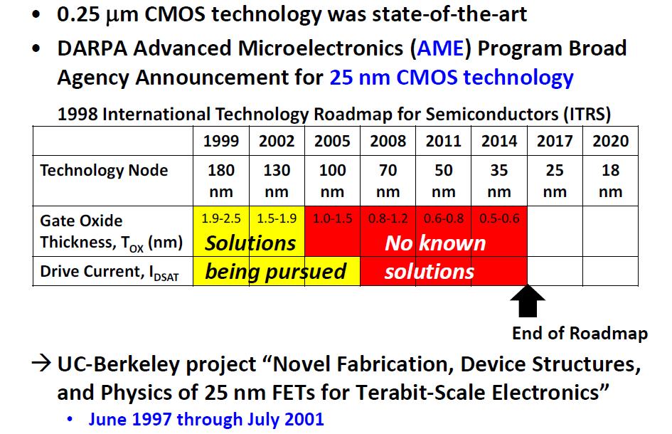
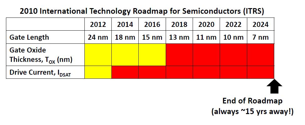

45 * Comparison of ITRS Roadmap on 1998 and 2010
MOSFET short channel effects
 MOSFET short channel effects overview Five different short channel effects can be distinguished: velocity saturation drain induced barrier lowering (DIBL) impact ionization surface scattering hot electrons
Session 10: Solid State Physics MOSFET
 Session 10: Solid State Physics MOSFET 1 Outline A B C D E F G H I J 2 MOSCap MOSFET Metal-Oxide-Semiconductor Field-Effect Transistor: Al (metal) SiO2 (oxide) High k ~0.1 ~5 A SiO2 A n+ n+ p-type Si (bulk)
Why Scaling? CPU speed Chip size R, C CPU can increase speed by reducing occupying area.
 Why Scaling? Higher density : Integration of more transistors onto a smaller chip : reducing the occupying area and production cost Higher Performance : Higher current drive : smaller metal to metal capacitance
Lecture 4. MOS transistor theory
 Lecture 4 MOS transistor theory 1.7 Introduction: A MOS transistor is a majority-carrier device, in which the current in a conducting channel between the source and the drain is modulated by a voltage
CONTENTS. 2.2 Schrodinger's Wave Equation 31. PART I Semiconductor Material Properties. 2.3 Applications of Schrodinger's Wave Equation 34
 CONTENTS Preface x Prologue Semiconductors and the Integrated Circuit xvii PART I Semiconductor Material Properties CHAPTER 1 The Crystal Structure of Solids 1 1.0 Preview 1 1.1 Semiconductor Materials
Lecture-45. MOS Field-Effect-Transistors Threshold voltage
 Lecture-45 MOS Field-Effect-Transistors 7.4. Threshold voltage In this section we summarize the calculation of the threshold voltage and discuss the dependence of the threshold voltage on the bias applied
Sub-Threshold Region Behavior of Long Channel MOSFET
 Sub-threshold Region - So far, we have discussed the MOSFET behavior in linear region and saturation region - Sub-threshold region is refer to region where Vt is less than Vt - Sub-threshold region reflects
6. LDD Design Tradeoffs on Latch-Up and Degradation in SOI MOSFET
 110 6. LDD Design Tradeoffs on Latch-Up and Degradation in SOI MOSFET An experimental study has been conducted on the design of fully depleted accumulation mode SOI (SIMOX) MOSFET with regard to hot carrier
MOSFET Terminals. The voltage applied to the GATE terminal determines whether current can flow between the SOURCE & DRAIN terminals.
 MOSFET Terminals The voltage applied to the GATE terminal determines whether current can flow between the SOURCE & DRAIN terminals. For an n-channel MOSFET, the SOURCE is biased at a lower potential (often
FET(Field Effect Transistor)
") Field Effect Transistor: Construction and Characteristic of JFETs. Transfer Characteristic. CS,CD,CG amplifier and analysis of CS amplifier MOSFET (Depletion and Enhancement) Type, Transfer Characteristic,
Field Effect Transistor: Construction and Characteristic of JFETs. Transfer Characteristic. CS,CD,CG amplifier and analysis of CS amplifier MOSFET (Depletion and Enhancement) Type, Transfer Characteristic,
MOSFET & IC Basics - GATE Problems (Part - I)
") MOSFET & IC Basics - GATE Problems (Part - I) 1. Channel current is reduced on application of a more positive voltage to the GATE of the depletion mode n channel MOSFET. (True/False) [GATE 1994: 1 Mark]
MOSFET & IC Basics - GATE Problems (Part - I) 1. Channel current is reduced on application of a more positive voltage to the GATE of the depletion mode n channel MOSFET. (True/False) [GATE 1994: 1 Mark]
Fin-Shaped Field Effect Transistor (FinFET) Min Ku Kim 03/07/2018
 Min Ku Kim 03/07/2018") Fin-Shaped Field Effect Transistor (FinFET) Min Ku Kim 03/07/2018 ECE 658 Sp 2018 Semiconductor Materials and Device Characterizations OUTLINE Background FinFET Future Roadmap Keeping up w/ Moore s Law
Fin-Shaped Field Effect Transistor (FinFET) Min Ku Kim 03/07/2018 ECE 658 Sp 2018 Semiconductor Materials and Device Characterizations OUTLINE Background FinFET Future Roadmap Keeping up w/ Moore s Law
Tunneling Field Effect Transistors for Low Power ULSI
 Tunneling Field Effect Transistors for Low Power ULSI Byung-Gook Park Inter-university Semiconductor Research Center and School of Electrical and Computer Engineering Seoul National University Outline
FUNDAMENTALS OF MODERN VLSI DEVICES
 19-13- FUNDAMENTALS OF MODERN VLSI DEVICES YUAN TAUR TAK H. MING CAMBRIDGE UNIVERSITY PRESS Physical Constants and Unit Conversions List of Symbols Preface page xi xiii xxi 1 INTRODUCTION I 1.1 Evolution
Three Terminal Devices
 Three Terminal Devices - field effect transistor (FET) - bipolar junction transistor (BJT) - foundation on which modern electronics is built - active devices - devices described completely by considering
Solid State Devices- Part- II. Module- IV
 Solid State Devices- Part- II Module- IV MOS Capacitor Two terminal MOS device MOS = Metal- Oxide- Semiconductor MOS capacitor - the heart of the MOSFET The MOS capacitor is used to induce charge at the
NAME: Last First Signature
 UNIVERSITY OF CALIFORNIA, BERKELEY College of Engineering Department of Electrical Engineering and Computer Sciences EE 130: IC Devices Spring 2003 FINAL EXAMINATION NAME: Last First Signature STUDENT
UNIT 3: FIELD EFFECT TRANSISTORS
 FIELD EFFECT TRANSISTOR: UNIT 3: FIELD EFFECT TRANSISTORS The field effect transistor is a semiconductor device, which depends for its operation on the control of current by an electric field. There are
MOSFET Parasitic Elements
 MOSFET Parasitic Elements Three MITs of the ay Components of the source resistance and their influence on g m and R d Gate-induced drain leakage (GIL) and its effect on lowest possible leakage current
Semiconductor TCAD Tools
 Device Design Consideration for Nanoscale MOSFET Using Semiconductor TCAD Tools Teoh Chin Hong and Razali Ismail Department of Microelectronics and Computer Engineering, Universiti Teknologi Malaysia,
Department of Electrical Engineering IIT Madras
 Department of Electrical Engineering IIT Madras Sample Questions on Semiconductor Devices EE3 applicants who are interested to pursue their research in microelectronics devices area (fabrication and/or
3-D Modelling of the Novel Nanoscale Screen-Grid Field Effect Transistor (SGFET)
") 3-D Modelling of the Novel Nanoscale Screen-Grid Field Effect Transistor (SGFET) Pei W. Ding, Kristel Fobelets Department of Electrical Engineering, Imperial College London, U.K. J. E. Velazquez-Perez
3-D Modelling of the Novel Nanoscale Screen-Grid Field Effect Transistor (SGFET) Pei W. Ding, Kristel Fobelets Department of Electrical Engineering, Imperial College London, U.K. J. E. Velazquez-Perez
FET. Field Effect Transistors ELEKTRONIKA KONTROL. Eka Maulana, ST, MT, M.Eng. Universitas Brawijaya. p + S n n-channel. Gate. Basic structure.
 FET Field Effect Transistors ELEKTRONIKA KONTROL Basic structure Gate G Source S n n-channel Cross section p + p + p + G Depletion region Drain D Eka Maulana, ST, MT, M.Eng. Universitas Brawijaya S Channel
Drive performance of an asymmetric MOSFET structure: the peak device
 MEJ 499 Microelectronics Journal Microelectronics Journal 30 (1999) 229 233 Drive performance of an asymmetric MOSFET structure: the peak device M. Stockinger a, *, A. Wild b, S. Selberherr c a Institute
Digital Electronics. By: FARHAD FARADJI, Ph.D. Assistant Professor, Electrical and Computer Engineering, K. N. Toosi University of Technology
 K. N. Toosi University of Technology Chapter 7. Field-Effect Transistors By: FARHAD FARADJI, Ph.D. Assistant Professor, Electrical and Computer Engineering, K. N. Toosi University of Technology http://wp.kntu.ac.ir/faradji/digitalelectronics.htm
Semiconductor Physics and Devices
 Nonideal Effect The experimental characteristics of MOSFETs deviate to some degree from the ideal relations that have been theoretically derived. Semiconductor Physics and Devices Chapter 11. MOSFET: Additional
Charge-Based Continuous Equations for the Transconductance and Output Conductance of Graded-Channel SOI MOSFET s
 Charge-Based Continuous Equations for the Transconductance and Output Conductance of Graded-Channel SOI MOSFET s Michelly de Souza 1 and Marcelo Antonio Pavanello 1,2 1 Laboratório de Sistemas Integráveis,
Field-Effect Transistor (FET) is one of the two major transistors; FET derives its name from its working mechanism;
 is one of the two major transistors; FET derives its name from its working mechanism;") Chapter 3 Field-Effect Transistors (FETs) 3.1 Introduction Field-Effect Transistor (FET) is one of the two major transistors; FET derives its name from its working mechanism; The concept has been known
Chapter 3 Field-Effect Transistors (FETs) 3.1 Introduction Field-Effect Transistor (FET) is one of the two major transistors; FET derives its name from its working mechanism; The concept has been known
4: Transistors Non idealities
 4: Transistors Non idealities Inversion Major cause of non-idealities/complexities: Who controls channel (and how)? Large Body(Substrate) Source Voltage V G V SB - - - - - - - - n+ n+ - - - - - - - - -
MOS TRANSISTOR THEORY
 MOS TRANSISTOR THEORY Introduction A MOS transistor is a majority-carrier device, in which the current in a conducting channel between the source and the drain is modulated by a voltage applied to the
MOS Capacitance and Introduction to MOSFETs
 ECE-305: Fall 2016 MOS Capacitance and Introduction to MOSFETs Professor Peter Bermel Electrical and Computer Engineering Purdue University, West Lafayette, IN USA pbermel@purdue.edu 11/4/2016 Pierret,
Solid State Device Fundamentals
 Solid State Device Fundamentals 4.4. Field Effect Transistor (MOSFET) ENS 463 Lecture Course by Alexander M. Zaitsev alexander.zaitsev@csi.cuny.edu Tel: 718 982 2812 4N101b 1 Field-effect transistor (FET)
4.1 Device Structure and Physical Operation
 10/12/2004 4_1 Device Structure and Physical Operation blank.doc 1/2 4.1 Device Structure and Physical Operation Reading Assignment: pp. 235-248 Chapter 4 covers Field Effect Transistors ( ) Specifically,
Power MOSFET Zheng Yang (ERF 3017,
 ECE442 Power Semiconductor Devices and Integrated Circuits Power MOSFET Zheng Yang (ERF 3017, email: yangzhen@uic.edu) Evolution of low-voltage (
Effect of Channel Doping Concentration on the Impact ionization of n- Channel Fully Depleted SOI MOSFET
 International Journal of Engineering Works Kambohwell Publisher Enterprises Vol. 2, Issue 2, PP. 18-22, Feb. 2015 www.kwpublisher.com Effect of Channel Doping Concentration on the Impact ionization of
Advanced MOSFET Basics. Dr. Lynn Fuller
 ROCHESTER INSTITUTE OF TECHNOLOGY MICROELECTRONIC ENGINEERING Advanced MOSFET Basics Dr. Lynn Fuller Webpage: http://people.rit.edu/lffeee 82 Lomb Memorial Drive Rochester, NY 14623-5604 Tel (585) 475-2035
Lecture 15. Field Effect Transistor (FET) Wednesday 29/11/2017 MOSFET 1-1
 Wednesday 29/11/2017 MOSFET 1-1") Lecture 15 Field Effect Transistor (FET) Wednesday 29/11/2017 MOSFET 1-1 Outline MOSFET transistors Introduction to MOSFET MOSFET Types epletion-type MOSFET Characteristics Comparison between JFET and
Lecture 15 Field Effect Transistor (FET) Wednesday 29/11/2017 MOSFET 1-1 Outline MOSFET transistors Introduction to MOSFET MOSFET Types epletion-type MOSFET Characteristics Comparison between JFET and
INTERNATIONAL JOURNAL OF APPLIED ENGINEERING RESEARCH, DINDIGUL Volume 1, No 3, 2010
 Low Power CMOS Inverter design at different Technologies Vijay Kumar Sharma 1, Surender Soni 2 1 Department of Electronics & Communication, College of Engineering, Teerthanker Mahaveer University, Moradabad
Reg. No. : Question Paper Code : B.E./B.Tech. DEGREE EXAMINATION, NOVEMBER/DECEMBER Second Semester
 WK 5 Reg. No. : Question Paper Code : 27184 B.E./B.Tech. DEGREE EXAMINATION, NOVEMBER/DECEMBER 2015. Time : Three hours Second Semester Electronics and Communication Engineering EC 6201 ELECTRONIC DEVICES
Field Effect Transistors (FET s) University of Connecticut 136
 University of Connecticut 136") Field Effect Transistors (FET s) University of Connecticut 136 Field Effect Transistors (FET s) FET s are classified three ways: by conduction type n-channel - conduction by electrons p-channel - conduction
Field Effect Transistors (FET s) University of Connecticut 136 Field Effect Transistors (FET s) FET s are classified three ways: by conduction type n-channel - conduction by electrons p-channel - conduction
I E I C since I B is very small
 Figure 2: Symbols and nomenclature of a (a) npn and (b) pnp transistor. The BJT consists of three regions, emitter, base, and collector. The emitter and collector are usually of one type of doping, while
FIELD EFFECT TRANSISTOR (FET) 1. JUNCTION FIELD EFFECT TRANSISTOR (JFET)
 1. JUNCTION FIELD EFFECT TRANSISTOR (JFET)") FIELD EFFECT TRANSISTOR (FET) The field-effect transistor (FET) is a three-terminal device used for a variety of applications that match, to a large extent, those of the BJT transistor. Although there
FIELD EFFECT TRANSISTOR (FET) The field-effect transistor (FET) is a three-terminal device used for a variety of applications that match, to a large extent, those of the BJT transistor. Although there
EECE 481. MOS Basics Lecture 2
 EECE 481 MOS Basics Lecture 2 Reza Molavi Dept. of ECE University of British Columbia reza@ece.ubc.ca Slides Courtesy : Dr. Res Saleh (UBC), Dr. D. Sengupta (AMD), Dr. B. Razavi (UCLA) 1 PN Junction and
UNIT-1 Fundamentals of Low Power VLSI Design
 UNIT-1 Fundamentals of Low Power VLSI Design Need for Low Power Circuit Design: The increasing prominence of portable systems and the need to limit power consumption (and hence, heat dissipation) in very-high
THE METAL-SEMICONDUCTOR CONTACT
 THE METAL-SEMICONDUCTOR CONTACT PROBLEM 1 To calculate the theoretical barrier height, built-in potential barrier, and maximum electric field in a metal-semiconductor diode for zero applied bias. Consider
EC0306 INTRODUCTION TO VLSI DESIGN
 EC0306 INTRODUCTION TO VLSI DESIGN UNIT I INTRODUCTION TO MOS CIRCUITS Why VLSI? Integration improves the design: o lower parasitics = higher speed; o lower power; o physically smaller. Integration reduces
3: MOS Transistors. Non idealities
 3: MOS Transistors Non idealities Inversion Major cause of non-idealities/complexities: Who controls channel (and how)? Large Body(Substrate) Source Voltage V G V SB - - - - - - - - n+ n+ - - - - - - -
ECE520 VLSI Design. Lecture 2: Basic MOS Physics. Payman Zarkesh-Ha
 ECE520 VLSI Design Lecture 2: Basic MOS Physics Payman Zarkesh-Ha Office: ECE Bldg. 230B Office hours: Wednesday 2:00-3:00PM or by appointment E-mail: pzarkesh@unm.edu Slide: 1 Review of Last Lecture Semiconductor
Alternative Channel Materials for MOSFET Scaling Below 10nm
 Alternative Channel Materials for MOSFET Scaling Below 10nm Doug Barlage Electrical Requirements of Channel Mark Johnson Challenges With Material Synthesis Introduction Outline Challenges with scaling
Alternatives to standard MOSFETs. What problems are we really trying to solve?
 Alternatives to standard MOSFETs A number of alternative FET schemes have been proposed, with an eye toward scaling up to the 10 nm node. Modifications to the standard MOSFET include: Silicon-in-insulator
CHAPTER 2 LITERATURE REVIEW
 CHAPTER 2 LITERATURE REVIEW 2.1 Introduction of MOSFET The structure of the MOS field-effect transistor (MOSFET) has two regions of doping opposite that of the substrate, one at each edge of the MOS structure
value of W max for the device. The at band voltage is -0.9 V. Problem 5: An Al-gate n-channel MOS capacitor has a doping of N a = cm ;3. The oxi
 Prof. Jasprit Singh Fall 2001 EECS 320 Homework 10 This homework is due on December 6 Problem 1: An n-type In 0:53 Ga 0:47 As epitaxial layer doped at 10 16 cm ;3 is to be used as a channel in a FET. A
MEASUREMENT AND INSTRUMENTATION STUDY NOTES UNIT-I
 MEASUREMENT AND INSTRUMENTATION STUDY NOTES The MOSFET The MOSFET Metal Oxide FET UNIT-I As well as the Junction Field Effect Transistor (JFET), there is another type of Field Effect Transistor available
3084 IEEE TRANSACTIONS ON NUCLEAR SCIENCE, VOL. 60, NO. 4, AUGUST 2013
 3084 IEEE TRANSACTIONS ON NUCLEAR SCIENCE, VOL. 60, NO. 4, AUGUST 2013 Dummy Gate-Assisted n-mosfet Layout for a Radiation-Tolerant Integrated Circuit Min Su Lee and Hee Chul Lee Abstract A dummy gate-assisted
International Journal of Scientific & Engineering Research, Volume 6, Issue 2, February-2015 ISSN
 Performance Evaluation and Comparison of Ultra-thin Bulk (UTB), Partially Depleted and Fully Depleted SOI MOSFET using Silvaco TCAD Tool Seema Verma1, Pooja Srivastava2, Juhi Dave3, Mukta Jain4, Priya
MOSFET FUNDAMENTALS OPERATION & MODELING
 MOSFET FUNDAMENTALS OPERATION & MODELING MOSFET MODELING AND OPERATION MOSFET Fundamentals MOSFET Physical Structure and Operation MOSFET Large Signal I-V Characteristics Subthreshold Triode Saturation
INTRODUCTION: Basic operating principle of a MOSFET:
 INTRODUCTION: Along with the Junction Field Effect Transistor (JFET), there is another type of Field Effect Transistor available whose Gate input is electrically insulated from the main current carrying
Review Energy Bands Carrier Density & Mobility Carrier Transport Generation and Recombination
 Review Energy Bands Carrier Density & Mobility Carrier Transport Generation and Recombination Current Transport: Diffusion, Thermionic Emission & Tunneling For Diffusion current, the depletion layer is
Field Effect Transistor (FET) FET 1-1
 FET 1-1") Field Effect Transistor (FET) FET 1-1 Outline MOSFET transistors ntroduction to MOSFET MOSFET Types epletion-type MOSFET Characteristics Biasing Circuits and Examples Comparison between JFET and epletion-type
Field Effect Transistor (FET) FET 1-1 Outline MOSFET transistors ntroduction to MOSFET MOSFET Types epletion-type MOSFET Characteristics Biasing Circuits and Examples Comparison between JFET and epletion-type
EE70 - Intro. Electronics
 EE70 - Intro. Electronics Course website: ~/classes/ee70/fall05 Today s class agenda (November 28, 2005) review Serial/parallel resonant circuits Diode Field Effect Transistor (FET) f 0 = Qs = Qs = 1 2π
EE301 Electronics I , Fall
 EE301 Electronics I 2018-2019, Fall 1. Introduction to Microelectronics (1 Week/3 Hrs.) Introduction, Historical Background, Basic Consepts 2. Rewiev of Semiconductors (1 Week/3 Hrs.) Semiconductor materials
EE 5611 Introduction to Microelectronic Technologies Fall Thursday, September 04, 2014 Lecture 02
 EE 5611 Introduction to Microelectronic Technologies Fall 2014 Thursday, September 04, 2014 Lecture 02 1 Lecture Outline Review on semiconductor materials Review on microelectronic devices Example of microelectronic
Assignment 1 SOLUTIONS
 ELEC5509 Assignment 1 SOLUTIONS September 2013 The nmos technology used in ELEC4609 provides enhancement MOSFETs with VT = 0.7V and depletion MOSFETs with VTd = -3.0V. The gate oxide thickness t ox = 50nm
Parameter Optimization Of GAA Nano Wire FET Using Taguchi Method
 Parameter Optimization Of GAA Nano Wire FET Using Taguchi Method S.P. Venu Madhava Rao E.V.L.N Rangacharyulu K.Lal Kishore Professor, SNIST Professor, PSMCET Registrar, JNTUH Abstract As the process technology
Lecture 13. Metal Oxide Semiconductor Field Effect Transistor (MOSFET) MOSFET 1-1
 MOSFET 1-1") Lecture 13 Metal Oxide Semiconductor Field Effect Transistor (MOSFET) MOSFET 1-1 Outline Continue MOSFET Qualitative Operation epletion-type MOSFET Characteristics Biasing Circuits and Examples Enhancement-type
Lecture 13 Metal Oxide Semiconductor Field Effect Transistor (MOSFET) MOSFET 1-1 Outline Continue MOSFET Qualitative Operation epletion-type MOSFET Characteristics Biasing Circuits and Examples Enhancement-type
UNIT 3 Transistors JFET
 UNIT 3 Transistors JFET Mosfet Definition of BJT A bipolar junction transistor is a three terminal semiconductor device consisting of two p-n junctions which is able to amplify or magnify a signal. It
ECE 440 Lecture 39 : MOSFET-II
 ECE 440 Lecture 39 : MOSFETII Class Outline: MOSFET Qualitative Effective Mobility MOSFET Quantitative Things you should know when you leave Key Questions How does a MOSFET work? Why does the channel mobility
EEC 216 Lecture #8: Leakage. Rajeevan Amirtharajah University of California, Davis
 EEC 216 Lecture #8: Leakage Rajeevan Amirtharajah University of California, Davis Outline Announcements Review: Low Power Interconnect Finish Lecture 7 Leakage Mechanisms Circuit Styles for Low Leakage
Electrical Characterization of a Second-gate in a Silicon-on-Insulator Transistor
 Electrical Characterization of a Second-gate in a Silicon-on-Insulator Transistor Antonio Oblea: McNair Scholar Dr. Stephen Parke: Faculty Mentor Electrical Engineering As an independent double-gate, silicon-on-insulator
Semiconductor Physics and Devices
 Metal-Semiconductor and Semiconductor Heterojunctions The Metal-Oxide-Semiconductor Field-Effect Transistor (MOSFET) is one of two major types of transistors. The MOSFET is used in digital circuit, because
Student Lecture by: Giangiacomo Groppi Joel Cassell Pierre Berthelot September 28 th 2004
 Student Lecture by: Giangiacomo Groppi Joel Cassell Pierre Berthelot September 28 th 2004 Lecture outline Historical introduction Semiconductor devices overview Bipolar Junction Transistor (BJT) Field
Davinci. Semiconductor Device Simulaion in 3D SYSTEMS PRODUCTS LOGICAL PRODUCTS PHYSICAL IMPLEMENTATION SIMULATION AND ANALYSIS LIBRARIES TCAD
 SYSTEMS PRODUCTS LOGICAL PRODUCTS PHYSICAL IMPLEMENTATION SIMULATION AND ANALYSIS LIBRARIES TCAD Aurora DFM WorkBench Davinci Medici Raphael Raphael-NES Silicon Early Access TSUPREM-4 Taurus-Device Taurus-Lithography
8 English P.20 한국의 P.21 中 文 P.22
 8 English P. 20 한국의 P. 21 中文 P. 22 인터넷 시스템 이용가이드 络 统 0120-615-919 support@broad-e.co.jp http://b-cubic.com/user/ 英 :If you have any inquiries about settings or connection please contact the Internet
Future MOSFET Devices using high-k (TiO 2 ) dielectric
 dielectric") Future MOSFET Devices using high-k (TiO 2 ) dielectric Prerna Guru Jambheshwar University, G.J.U.S. & T., Hisar, Haryana, India, prernaa.29@gmail.com Abstract: In this paper, an 80nm NMOS with high-k (TiO
Future MOSFET Devices using high-k (TiO 2 ) dielectric Prerna Guru Jambheshwar University, G.J.U.S. & T., Hisar, Haryana, India, prernaa.29@gmail.com Abstract: In this paper, an 80nm NMOS with high-k (TiO
97.398*, Physical Electronics, Lecture 21. MOSFET Operation
 97.398*, Physical Electronics, Lecture 21 MOSFET Operation Lecture Outline Last lecture examined the MOSFET structure and required processing steps Now move on to basic MOSFET operation, some of which
Fundamentals of Power Semiconductor Devices
 В. Jayant Baliga Fundamentals of Power Semiconductor Devices 4y Spri ringer Contents Preface vii Chapter 1 Introduction 1 1.1 Ideal and Typical Power Switching Waveforms 3 1.2 Ideal and Typical Power Device
INTRODUCTION TO MOS TECHNOLOGY
 INTRODUCTION TO MOS TECHNOLOGY 1. The MOS transistor The most basic element in the design of a large scale integrated circuit is the transistor. For the processes we will discuss, the type of transistor
V A ( ) 2 = A. For Vbe = 0.4V: Ic = 7.34 * 10-8 A. For Vbe = 0.5V: Ic = 3.49 * 10-6 A. For Vbe = 0.6V: Ic = 1.
 2 = A. For Vbe = 0.4V: Ic = 7.34 * 10-8 A. For Vbe = 0.5V: Ic = 3.49 * 10-6 A. For Vbe = 0.6V: Ic = 1.") 1. A BJT has the structure and parameters below. a. Base Width = 0.5mu b. Electron lifetime in base is 1x10⁻⁷ sec c. Base doping is NA=10 17 /cm 3 d. Emitter Doping is ND=2 x10 19 /cm 3. Collector Doping
1. A BJT has the structure and parameters below. a. Base Width = 0.5mu b. Electron lifetime in base is 1x10⁻⁷ sec c. Base doping is NA=10 17 /cm 3 d. Emitter Doping is ND=2 x10 19 /cm 3. Collector Doping
Contents. Contents... v. Preface... xiii. Chapter 1 Introduction...1. Chapter 2 Significant Physical Effects In Modern MOSFETs...
 Contents Contents... v Preface... xiii Chapter 1 Introduction...1 1.1 Compact MOSFET Modeling for Circuit Simulation...1 1.2 The Trends of Compact MOSFET Modeling...5 1.2.1 Modeling new physical effects...5
PHYSICS OF SEMICONDUCTOR DEVICES
 PHYSICS OF SEMICONDUCTOR DEVICES PHYSICS OF SEMICONDUCTOR DEVICES by J. P. Colinge Department of Electrical and Computer Engineering University of California, Davis C. A. Colinge Department of Electrical
Scaling Of Si MOSFETs For Digital Applications
 Scaling Of Si MOSFETs For Digital Applications By Dustin K. Slisher, Ronald G. Filippi, Jr., Daniel W. Storaska and Alberto H. Gay Final Project in the Advanced Concepts in Electronic and Optoelectronic
Depletion-mode operation ( 공핍형 ): Using an input gate voltage to effectively decrease the channel size of an FET
: Using an input gate voltage to effectively decrease the channel size of an FET") Ch. 13 MOSFET Metal-Oxide-Semiconductor Field-Effect Transistor : I D D-mode E-mode V g The gate oxide is made of dielectric SiO 2 with e = 3.9 Depletion-mode operation ( 공핍형 ): Using an input gate voltage
Ch. 13 MOSFET Metal-Oxide-Semiconductor Field-Effect Transistor : I D D-mode E-mode V g The gate oxide is made of dielectric SiO 2 with e = 3.9 Depletion-mode operation ( 공핍형 ): Using an input gate voltage
Design and Analysis of Double Gate MOSFET Devices using High-k Dielectric
 International Journal of Electrical Engineering. ISSN 0974-2158 Volume 7, Number 1 (2014), pp. 53-60 International Research Publication House http://www.irphouse.com Design and Analysis of Double Gate
Channel Engineering for Submicron N-Channel MOSFET Based on TCAD Simulation
 Australian Journal of Basic and Applied Sciences, 2(3): 406-411, 2008 ISSN 1991-8178 Channel Engineering for Submicron N-Channel MOSFET Based on TCAD Simulation 1 2 3 R. Muanghlua, N. Vittayakorn and A.
Optimization of Threshold Voltage for 65nm PMOS Transistor using Silvaco TCAD Tools
 IOSR Journal of Electrical and Electronics Engineering (IOSR-JEEE) e-issn: 2278-1676,p-ISSN: 2320-3331, Volume 6, Issue 1 (May. - Jun. 2013), PP 62-67 Optimization of Threshold Voltage for 65nm PMOS Transistor
Big Data and High Performance Computing
 Big Data and High Performance Computing Big data and high performance computing focus on academic research and technology development in areas of high performance computing platform architecture, parallel
Lecture 31 - The Short Metal-Oxide-Semiconductor Field-Effect Transistor (cont.) April 25, 2007
 April 25, 2007") 6.720J/3.43J - Integrated Microelectronic Devices - Spring 2007 Lecture 31-1 Lecture 31 - The Short Metal-Oxide-Semiconductor Field-Effect Transistor (cont.) April 25, 2007 Contents: 1. Short-channel effects
6.720J/3.43J - Integrated Microelectronic Devices - Spring 2007 Lecture 31-1 Lecture 31 - The Short Metal-Oxide-Semiconductor Field-Effect Transistor (cont.) April 25, 2007 Contents: 1. Short-channel effects
Performance Evaluation of MISISFET- TCAD Simulation
 Performance Evaluation of MISISFET- TCAD Simulation Tarun Chaudhary Gargi Khanna Rajeevan Chandel ABSTRACT A novel device n-misisfet with a dielectric stack instead of the single insulator of n-mosfet
Session 3: Solid State Devices. Silicon on Insulator
 Session 3: Solid State Devices Silicon on Insulator 1 Outline A B C D E F G H I J 2 Outline Ref: Taurand Ning 3 SOI Technology SOl materials: SIMOX, BESOl, and Smart Cut SIMOX : Synthesis by IMplanted
Stars Snub Twilight Premiere 明星怠慢 暮光之城 首映式
 Stars Snub Twilight Premiere 明星怠慢 暮光之城 首映式 1 Stars Snub Twilight Premiere 明星怠慢 暮光之城 首映式 Dedicated Fans Left Disappointed 忠实的粉丝们大失所望 Read the text below and do the activity that follows. 阅读下面的短文, 然后完成练习
ECE 5745 Complex Digital ASIC Design Topic 2: CMOS Devices
 ECE 5745 Complex Digital ASIC Design Topic 2: CMOS Devices Christopher Batten School of Electrical and Computer Engineering Cornell University http://www.csl.cornell.edu/courses/ece5950 Simple Transistor
UNIVERSITY OF CALIFORNIA AT BERKELEY College of Engineering Department of Electrical Engineering and Computer Sciences.
 UNIVERSITY OF CALIFORNIA AT BERKELEY College of Engineering Department of Electrical Engineering and Computer Sciences Discussion #9 EE 05 Spring 2008 Prof. u MOSFETs The standard MOSFET structure is shown
Electronics Review Flashcards
 November 21, 2011 1 Op Amps 2 Diodes 3 Silicon 4 pn Junctions 5 BJTs 6 MOSFETs Open Loop Characteristics Open-Loop Op-Amp Characteristics (first-order model) Closed Loop Characteristics Closed-Loop Op-Amp
Mechatronics and Measurement. Lecturer:Dung-An Wang Lecture 2
 Mechatronics and Measurement Lecturer:Dung-An Wang Lecture 2 Lecture outline Reading:Ch3 of text Today s lecture Semiconductor 2 Diode 3 4 Zener diode Voltage-regulator diodes. This family of diodes exhibits
Learning Outcomes. Spiral 2-6. Current, Voltage, & Resistors DIODES
 26.1 26.2 Learning Outcomes Spiral 26 Semiconductor Material MOS Theory I underst why a diode conducts current under forward bias but does not under reverse bias I underst the three modes of operation
Objective Type Questions 1. Why pure semiconductors are insulators at 0 o K? 2. What is effect of temperature on barrier voltage? 3.
 Objective Type Questions 1. Why pure semiconductors are insulators at 0 o K? 2. What is effect of temperature on barrier voltage? 3. What is difference between electron and hole? 4. Why electrons have
cost and reliability; power considerations were of secondary importance. In recent years. however, this has begun to change and increasingly power is
 CHAPTER-1 INTRODUCTION AND SCOPE OF WORK 1.0 MOTIVATION In the past, the major concern of the VLSI designer was area, performance, cost and reliability; power considerations were of secondary importance.
A BRIEF STUDY ON CHALLENGES OF MOSFET AND EVOLUTION OF FINFETS
 A BRIEF STUDY ON CHALLENGES OF MOSFET AND EVOLUTION OF FINFETS ABSTRACT J.Shailaja 1, Y.Priya 2 1 ECE Department, Sphoorthy Engineering College (India) 2 ECE,Sphoorthy Engineering College, (India) The
ITT Technical Institute. ET215 Devices 1. Unit 8 Chapter 4, Sections
 ITT Technical Institute ET215 Devices 1 Unit 8 Chapter 4, Sections 4.4 4.5 Chapter 4 Section 4.4 MOSFET Characteristics A Metal-Oxide semiconductor field-effect transistor is the other major category of
Performance Comparison of CMOS and Finfet Based Circuits At 45nm Technology Using SPICE
 RESEARCH ARTICLE OPEN ACCESS Performance Comparison of CMOS and Finfet Based Circuits At 45nm Technology Using SPICE Mugdha Sathe*, Dr. Nisha Sarwade** *(Department of Electrical Engineering, VJTI, Mumbai-19)