Front-To-Back MMIC Design Flow with ADS. Speed MMICs to market Save money and achieve high yield
|
|
|
- Avice Johns
- 6 years ago
- Views:
Transcription

1 Front-To-Back MMIC Design Flow with ADS Speed MMICs to market Save money and achieve high yield 1
2 Unique Tools for Robust Designs, First Pass, and High Yield Yield Sensitivity Histogram (YSH) to components 2
3 Agilent EEsof MMIC Foundry Partners All ADS kits are built and certified by foundries Atmel austriamicrosystems Bookham Technology Cree, Inc. Filtronic Compound Semiconductors Global Communication Semiconductors, Inc. (GCS) IHP Microelectronics Infineon IBM Microelectronics Jazz Semiconductor Knowledge*on Semiconductor Maxim Integrated Products Northrop Grumman Electronic Systems Northrop Grumman (Velocium) MagnaChip Semiconductor Ommic Peregrine Semiconductor Raytheon RF Components Philips Electronics N.V. Semiconductor Manufacturing International Corporation (SMIC) STMicroelectronics Triquint UMC UMS TSMC WIN X-FAB 3


4 Advanced Tools Seamlessly Integrated in ADS Convolution Circuit Envelope Phase Noise at VCO s Output Linear Simulator Planar EM Momentum Phase Noise at Divider s Output AM Noise at Divider s Output Harmonic Balance FEM 3D EM (EMDS) 3D Features includes 3D JDEC Bond Wire 4

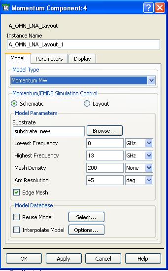
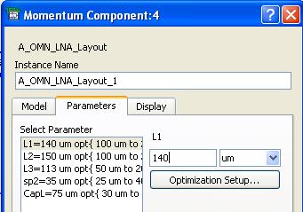
5 True MMIC Verification Prior to Manufacturing True MMIC Design Verification prior to Manufacturing is done by Co-simulating the MMIC inside the package and with bond wires using EMDS in ADS 2008 EMDS JDEC Bond Wire 5
6 PA Verification to Wireless Standards Realistic Input Signals and test benches for all Wireless Standards WIMAX Transmit Source PA Verification to wireless Standards PA 6
7 ADS Complete Front-to-Back MMIC Design Flow Part 1 Schematic Entry 7
8 Agilent EEsof EDA MMIC Foundry Partners All ADS Kits are built and Certified by Foundries Knowledge*on Gaetec The only complete MMIC PDK offering in the EDA Market, that is fully supported, maintained, and regularly updated by the foundries. If we don t have the PDK kit you need, we ll create it for you! 8


9 Advanced Model Composer (AMC) Technology AMC brings the accuracy of EM simulation and the speed of analytical models into a single, user-defined, compact model. Arbitrary user-defined parameterized shapes Generates model, symbol & layout 9

10 Example: TriQuint MASC Design Kit Valid Range of models EM based Inductor Models Using AMC Technology 10


11 Fully Parameterized Lines and Discontinuities Initial Line Lines Information contain Layers and current density Modifying the line by inserting an air-bridge with an offset and angle 11
12 12 Example: LNA - TriQuint MASC Design Kit
13 13 ADS Complete Front-to-Back MMIC Design Flow


14 Demo example Ku-band LNA Front End Design FET Characterization 14

15 Front End Design Biasing, Stability, Max Gain, Noise and Gain Circles 15
16 Front End Design 16

17 Impedance Matching 17

18 Front End Design 18
19 Front End Design 19
20 Front End Design 20

21 Front End Initial Design Yield Analysis 21
22 ADS Complete Front-to-Back MMIC Design Flow DFM 22
23 The Value of ADS DFM Technology Designing circuits that will work no matter what First to market First pass success High manufacturing yield (Lower cost per chip) ADS DFM Tools Tremendous amount of time and $$ savings Insensitive to changes in temp and supply voltage Reliable, high quality designs The only EDA company with unique DFM design tools that allow MMIC designers to create and manufacture robust circuits with first-pass success and high yield 23
 Used a standard design technique 2) Used a DFM Based design technique All designs went through the same Wafer Fab")
24 Real MMIC Designs Fabricated on the Same Wafer Actual real-world examples A reticle contains a few circuits, stepped and repeated across the whole wafer Amp1 Amp2 U/C 1 macro U/C 2 macro 1) Used a standard design technique 2) Used a DFM Based design technique All designs went through the same Wafer Fab Process 24

25 K-Band Up Converter Wafer Probed Results Mixer 1 Mixer 2 X-band Amp1 K-band X-band Amp2 K-band Ku-band LO Ku-band LO U/C 1 Macrocell / Standard Design U/C 2 Macrocell / DOE Based Design 25


26 Wafer Probed Results Note: Foundry process shifted to the left during this run. Amp2 shift was less sensitive to this shift Amp1 Standard Design Amp2 DFM based Design Amp1 Amp2 26

27 Understanding the Difference Amp2 Amp1 27

28 ADS Matching Tool Helps find Robust & High Yield Networks 19 different networks with different topologies to choose from They all include DFM analysis! 28

 to")
29 Using DFM Techniques On a Demo One-Stage LNA Yield Sensitivity Histogram (YSH) to components 29


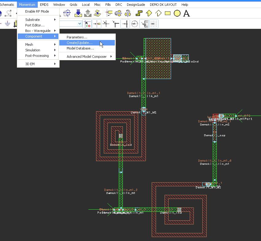
30 Using DFM Techniques to Transform One-Stage LNA into a Robust Design with High Yield 30
31 ADS Complete Front-to-Back MMIC Design Flow PA Verification 31
32 PA Verification to Wireless Standards Realistic input signals and test benches for all wireless standards WIMAX Transmit Source PA Verification to wireless Standards PA The most accurate and only tool set that provides true circuit verification to all wireless standards pre- and post-fabrication. Helps designers not only test and verify their designs, but also get the most performance out of their circuits. 32
33 An Example WIMAX PA EVM verification and spectrum Insert WiMAX PA into the Wireless Test Bench and press simulate 33
34 An Example WIMAX PA Small signal gain, S11 and Pin/Pout 34
35 Example WiMAX PA EVM Verification Fast verification! Simulation Time 20 minutes Fast Cosim (AVM) Not Used Simulation Time < 20 seconds Using Fast Cosim (AVM) 35
36 Example WiMAX PA Spectrum 36
37 Swept EVM and Statistical Analysis Easy Statistical Analysis on PA Verification at the System Level 50 Monte Carlo trials 10 minutes 2GB RAM Sweeping EVM as a function of Input Power, Pin 37
38 ADS Complete Front-to-Back MMIC Design Flow Part II Physical Design 38
39 Advanced Backend Physical Design Capability Schematic/Layout Synchronization ADS 2008 Layout Synchronization Simulating Layout in Schematic page Layout / Schematic Design Differences Physical Connectivity Engine OR Lay-con DRC Planar and 3D EM Tools 39

40 Advanced Backend Physical Design Capability Total flexibility with three synchronization modes ADS provides three different synchronization modes between schematic & layout, providing optimum flexibility in the development of MMICs Designers are not constrained by always having schematic and layout automatically synchronized Ability to switch back and forth between the three different modes Allows you to efficiently and accurately fit many elements designs into small areas. The result is a smaller die size and lowered overall cost per chip. 40


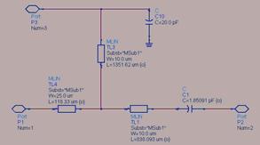
41 Advanced Backend Physical Design Capability Schematic/layout look-alike Original Schematic Synchronized Layout for Momentum EM Simulation & Optimization Layout look alike Used in the schematic page as: Full or Sub-network Graphical Cell Compiler with parameterized variables Advanced Model Composer with parameterized variables 41

42 New Transparency to Layer Configuration Improved layout visibility for multilayer MMIC designs Easier to see through the multilayer designs such as traces, grounds, and vias Before After 42


43 Advanced Backend Physical Design Capability Design differences Identifies Components in Layout not in Schematic Components in Schematic not in Layout Parameter Differences Nodal Mismatches 43


44 Advanced Backend Physical Design Capability Check layout vs. schematic and check layout for errors Custom LVS Utility Program 44

45 Advanced Backend Physical Design Capability Check physical connectivity (LayCon) Physical Connectivity Engine allows you to check your layout for any errors. This capacitor is not shorted. It is fine. This capacitor is shorted. It is shown by the metallization run. 45
 Problem")
46 Advanced Backend Physical Design Capability Check physical connectivity (LayCon) Problem Fixed 46


47 Advanced Backend Physical Design Capability Building reticles in ADS (TriQuint Foundry) 47

48 Advanced Backend Physical Design Capability EM simulation with Momentum and EMDS Spiral inductors are the largest devices on-chip and probably least understood. Spiral Inductors, Transformers, and Transmission Lines are important to model accurately in MMIC. Bond wires and package effects are very important to design to and verify to. Remember, the MMIC doesn t end at the chip level. Both Momentum Planar EM simulator and EMDS 3-D finite-element EM simulator are both seamlessly integrated in ADS and can insure your design success. 48
49 Momentum EM Simulation Accuracy and speed pays off Industrie s first 64-bit 3D planar EM solver Improved thick conductor modeling: Now includes the addition of horizontal current modeling on the metal interconnects sidewalls as well as the vertical currents. Adding a new Krylov Iterative Solver: Momentum now hosts three unique solvers to address the varying degrees of EM modeling complexity and extend EM modeling efficiencies across a much wider application coverage area. 49


50 LNA Layout & Momentum Simulation on the OMN of our one Stage LNA 50
51 LNA Simulation Results with Momentum Simulation on the OMN of LNA No Change in NF Momentum Circuit model 51
52 Momentum Optimization on LNA OMN 52


53 Momentum Optimization on LNA OMN Meshing during Momentum dimulation and optimization Output matching metwork parameterized layout look-alike component for EM simulation and optimization 53
54 Momentum Optimized Results Results achieved by reduction in line lengths and the series spiral inductor 54

55 EMDS Integration into ADS 3D Features includes 3D JDEC Bond Wire EMDS is now Seamlessly Integrated in ADS Follows the Momentum Model 55
56 Advanced 3D EM Simulation with EMDS Co-simulation of a balanced MMIC Amp inside a 10-pin package Efficient approach to package modeling is to Co-simulate the MMIC circuit design inside the package using EMDS in ADS. EMDS accurately models package parasitic and its effects on the MMIC Chip Performance. Co-Simulation / Optimization automatically adjusts the design s parameters and brings back its performance by counteracting the effect of the package parasitic 56
57 True MMIC Verification prior to Manufacturing Our LNA Example True MMIC design verification prior to manufacturing is done by co-simulating the MMIC inside the package and with bond wires using EMDS in ADS 3D View 57

58 True MMIC Verification Before Manufacturing You can co-simulate and optimize the response in the same way as in Momentum. 58

59 Advanced Backend Physical Design Capability Design Rule Check (DRC) Automatically Finds the Rules file location Automatically Loads the Rules file All you have to do Is to click on Run 59

60 Advanced Backend Physical Design Capability Design Rule Check (DRC) Users now can Load, Run, Compile, and View Results in one mouse click. Users can sort errors and can choose to view any error first. DRC provides exact error coordinates and lets you pan and zoom. 60


61 3D Pre-Viewer with Z-scale Expansion Scale up substrate thicknesses to easily visualize a complex 3D layout ADS 3D View Up-scaled View 61


62 3D Previewer with Cut Plane Cut through the layout to easily visualize a complex 3D layout 3 cut planes on XY, YZ, and XZ plane Flip Cut positive or negative cut No Cut Plane Enabled YZ Cut Plane Enabled 62


63 New Drag and Drop From Project View Window Drag and drop existing designs to the current design Both for Schematic and Layout Drag and drop designs directly from the Project View window No need to browse the library browser Drag and Drop 63

 Automatically inserts the via when")
64 Trace With Automatic Via Insertion Easier to change trace layers with hot keys, comma(,) and period(.) Automatically inserts the via when changing layers. 3D view 2D view 64


65 ADS Data Display is Another Design Tool Post Processing and Data Display RF specific functionality and flexibility to post-process and display data, for better insight to the circuit behavior. A design tool helps achieve faster design cycles 65
Innovations in EDA Webcast Series
 Welcome Innovations in EDA Webcast Series August 2, 2012 Jack Sifri MMIC Design Flow Specialist IC, Laminate, Package Multi-Technology PA Module Design Methodology Realizing the Multi-Technology Vision
When Should You Apply 3D Planar EM Simulation?
 When Should You Apply 3D Planar EM Simulation? Agilent EEsof EDA IMS 2010 MicroApps Andy Howard Agilent Technologies 1 3D planar EM is now much more of a design tool Solves bigger problems and runs faster
RF Board Design for Next Generation Wireless Systems
 RF Board Design for Next Generation Wireless Systems Page 1 Introduction Purpose: Provide basic background on emerging WiMax standard Introduce a new tool for Genesys that will aide in the design and verification
Design for Yield (DFY)
") Creating Robust Designs using Statistical Methods Design for Yield (DFY) Page 1 Creating Robust Designs using Statistical Methods What is a Robust Design? A design that is less sensitive to the manufacturing
Creating Robust Designs using Statistical Methods Design for Yield (DFY) Page 1 Creating Robust Designs using Statistical Methods What is a Robust Design? A design that is less sensitive to the manufacturing
60 GHZ PA Design Wireless HDMI/WPAN Application. Demonstrate Complete MMIC ADS Desktop Design Flow
 60 GHz Power Amplifier Design for Wireless HDMI (WPAN) Agilent EEsof EDA Innovative Solutions, Breakthrough Results Michael Thompson US Application Engineer District Manager October 13, 2009 Agilent Technologies,
The wireless industry
 From May 2007 High Frequency Electronics Copyright Summit Technical Media, LLC RF SiP Design Verification Flow with Quadruple LO Down Converter SiP By HeeSoo Lee and Dean Nicholson Agilent Technologies
AWR. SIP Flow White Paper UNDERSTANDING AVAILABLE TOOLS FOR RF SYSTEM-IN-PACKAGE AND MULTI-CHIP-MODULE DESIGN AND OPTIMIZATION
 UNDERSTANDING AVAILABLE TOOLS FOR RF SYSTEM-IN-PACKAGE AND MULTI-CHIP-MODULE DESIGN AND OPTIMIZATION RF system-in-package (SiP) and multi-chip-module (MCM) designs present engineers with the challenge
Agilent EEsof EDA. Enabling First Pass Success. Chee Keong, Teo Business Development Manager EEsof South Asia. Agilent Restricted
 Agilent EEsof EDA Enabling First Pass Success Chee Keong, Teo Business Development Manager EEsof South Asia EEsof EDA is Strategic to Agilent Technologies As the world s premier measurement company, Agilent
Using GoldenGate to Verify and Improve Your Designs Using Real Signals
 Using GoldenGate to Verify and Improve Your Designs Using Real Signals Enabling more complete understanding of your designs Agilent EEsof EDA 1 Outline What problems do designers face? Main point of this
Methodology for MMIC Layout Design
 17 Methodology for MMIC Layout Design Fatima Salete Correra 1 and Eduardo Amato Tolezani 2, 1 Laboratório de Microeletrônica da USP, Av. Prof. Luciano Gualberto, tr. 3, n.158, CEP 05508-970, São Paulo,
Chapter 6. Case Study: 2.4-GHz Direct Conversion Receiver. 6.1 Receiver Front-End Design
 Chapter 6 Case Study: 2.4-GHz Direct Conversion Receiver The chapter presents a 0.25-µm CMOS receiver front-end designed for 2.4-GHz direct conversion RF transceiver and demonstrates the necessity and
--- An integrated 3D EM design flow for EM/Circuit Co-Design
 ADS users group meeting 2009 Rome 13/05, Böblingen 14-15/05, Massy 16/06 --- An integrated 3D EM design flow for EM/Circuit Co-Design Motivations and drivers for co-design Throw-The-Die-Over-The-Wall,
Synthesis of Optimal On-Chip Baluns
 Synthesis of Optimal On-Chip Baluns Sharad Kapur, David E. Long and Robert C. Frye Integrand Software, Inc. Berkeley Heights, New Jersey Yu-Chia Chen, Ming-Hsiang Cho, Huai-Wen Chang, Jun-Hong Ou and Bigchoug
Using Sonnet EM Analysis with Cadence Virtuoso in RFIC Design. Sonnet Application Note: SAN-201B July 2011
 Using Sonnet EM Analysis with Cadence Virtuoso in RFIC Design Sonnet Application Note: SAN-201B July 2011 Description of Sonnet Suites Professional Sonnet Suites Professional is an industry leading full-wave
MMIC/RFIC Packaging Challenges Webcast (July 28, AM PST 12PM EST)
") MMIC/RFIC Packaging Challenges Webcast ( 9AM PST 12PM EST) Board Package Chip HEESOO LEE Agilent EEsof 3DEM Technical Lead 1 Agenda 1. MMIC/RFIC packaging challenges 2. Design techniques and solutions
MMIC/RFIC Packaging Challenges Webcast ( 9AM PST 12PM EST) Board Package Chip HEESOO LEE Agilent EEsof 3DEM Technical Lead 1 Agenda 1. MMIC/RFIC packaging challenges 2. Design techniques and solutions
Microwave and RF Engineering
 Microwave and RF Engineering Volume 1 An Electronic Design Automation Approach Ali A. Behagi and Stephen D. Turner BT Microwave LLC State College, PA 16803 Copyrighted Material Microwave and RF Engineering
EDA Toolsets for RF Design & Modeling
 Yiannis Moisiadis, Errikos Lourandakis, Sotiris Bantas Helic, Inc. 101 Montgomery str., suite 1950 San Fransisco, CA 94104, USA Email: {moisiad, lourandakis, s.bantas}@helic.com Abstract This paper presents
Low Noise Amplifier Design Methodology Summary By Ambarish Roy, Skyworks Solutions, Inc.
 February 2014 Low Noise Amplifier Design Methodology Summary By Ambarish Roy, Skyworks Solutions, Inc. Low Noise Amplifiers (LNAs) amplify weak signals received by the antenna in communication systems.
Modeling Physical PCB Effects 5&
 Abstract Getting logical designs to meet specifications is the first step in creating a manufacturable design. Getting the physical design to work is the next step. The physical effects of PCB materials,
Design and Layout of a X-Band MMIC Power Amplifier in a Phemt Technology
 Design and Layout of a X-Band MMIC Power Amplifier in a Phemt Technology Renbin Dai, and Rana Arslan Ali Khan Abstract The design of Class A and Class AB 2-stage X band Power Amplifier is described in
RFIC DESIGN EXAMPLE: MIXER
 APPENDIX RFI DESIGN EXAMPLE: MIXER The design of radio frequency integrated circuits (RFIs) is relatively complicated, involving many steps as mentioned in hapter 15, from the design of constituent circuit
Multilayer VIA simulations using ADS Anurag Bhargava, Application Consultant, Agilent EEsof EDA, Agilent Technologies
 Multilayer VIA simulations using ADS Anurag Bhargava, Application Consultant, Agilent EEsof EDA, Agilent Technologies Many a time designers find themselves in pretty confusing start when it comes to simulating
DATASHEET CADENCE QRC EXTRACTION
 DATASHEET Cadence QRC Etraction, the industry s premier 3D fullchip parasitic etractor that is independent of design style or flow, is a fast and accurate RLCK etraction solution used during design implementation
Controlled Impedance Line Designer
 Heidi Barnes WW HSD Application Engineer Controlled Impedance Line Designer Stephen Slater HSD Product Manager EDA Simulation Tools for Power Integrity Agenda 1. Designing a channel for a desired impedance
Bridging the Gap between System & Circuit Designers
 Bridging the Gap between System & Circuit Designers October 27, 2004 Presented by: Kal Kalbasi Q & A Marc Petersen Copyright 2003 Agilent Technologies, Inc. The Gap System Communication System Design System
Agilent EEsof EDA.
 Agilent EEsof EDA This document is owned by Agilent Technologies, but is no longer kept current and may contain obsolete or inaccurate references. We regret any inconvenience this may cause. For the latest
Dual-band LNA Design for Wireless LAN Applications. 2.4 GHz LNA 5 GHz LNA Min Typ Max Min Typ Max
 Dual-band LNA Design for Wireless LAN Applications White Paper By: Zulfa Hasan-Abrar, Yut H. Chow Introduction Highly integrated, cost-effective RF circuitry is becoming more and more essential to the
Advances in Microwave & Millimeterwave Integrated Circuits
 الراديو - جامعة Advances in Microwave & Millimeterwave Integrated Circuits الهندسة آلية عين شمس ١٥ مارس ٢٠٠٧-١٣ Amin K. Ezzeddine AMCOM Communications, Inc. 22300 Comsat Drive Clarksburg, Maryland 20871,
Direct-Conversion I-Q Modulator Simulation by Andy Howard, Applications Engineer Agilent EEsof EDA
 Direct-Conversion I-Q Modulator Simulation by Andy Howard, Applications Engineer Agilent EEsof EDA Introduction This article covers an Agilent EEsof ADS example that shows the simulation of a directconversion,
Advanced Design System - Fundamentals. Mao Wenjie
 Advanced Design System - Fundamentals Mao Wenjie wjmao@263.net Main Topics in This Class Topic 1: ADS and Circuit Simulation Introduction Topic 2: DC and AC Simulations Topic 3: S-parameter Simulation
5-20GHz MMIC Amplifier with Integrated Bias
 5-20GHz MMIC Amplifier with Integrated Bias Features Excellent performance 5-18GHz: High, flat gain (15 ± 0.5dB) Good return loss (15dB) 17.5dBm P1dB, 20dBm Psat Mixed-signal 3.3V operation: Similar small-signal
Thank you for downloading one of our ANSYS whitepapers we hope you enjoy it.
 Thank you! Thank you for downloading one of our ANSYS whitepapers we hope you enjoy it. Have questions? Need more information? Please don t hesitate to contact us! We have plenty more where this came from.
Complete RF And Microwave Design Flow with AWR Design Environment. Tabish Khan, AWR Corporation
 Complete RF And Microwave Design Flow with AWR Design Environment Tabish Khan, AWR Corporation Traditional Serial Design Flow Separate tools, user interfaces, netlists and databases System Design Design
Final Circuit & System Simulation - with Optional
 Final Circuit & System Simulation - with Optional Co-Simulation Slide 9-1 What is the final topic in this class? Simulation of your amp_1900 and filters in the receiver system to verify analog performance.
Foundries, MMICs, systems. Rüdiger Follmann
 Foundries, MMICs, systems Rüdiger Follmann Content MMIC foundries Designs and trends Examples 2 Foundries and MMICs Feb-09 IMST GmbH - All rights reserved MMIC foundries Foundries IMST is a UMS certified
Application Note 5012
 MGA-61563 High Performance GaAs MMIC Amplifier Application Note 5012 Application Information The MGA-61563 is a high performance GaAs MMIC amplifier fabricated with Avago Technologies E-pHEMT process and
Design and Matching of a 60-GHz Printed Antenna
 Application Example Design and Matching of a 60-GHz Printed Antenna Using NI AWR Software and AWR Connected for Optenni Figure 1: Patch antenna performance. Impedance matching of high-frequency components
The Design of E-band MMIC Amplifiers
 The Design of E-band MMIC Amplifiers Liam Devlin, Stuart Glynn, Graham Pearson, Andy Dearn * Plextek Ltd, London Road, Great Chesterford, Essex, CB10 1NY, UK; (lmd@plextek.co.uk) Abstract The worldwide
LUCEDA PHOTONICS DELIVERS A SILICON PHOTONICS IC SOLUTION IN TANNER L-EDIT
 LUCEDA PHOTONICS DELIVERS A SILICON PHOTONICS IC SOLUTION IN TANNER L-EDIT WIM BOGAERTS, PIETER DUMON, AND MARTIN FIERS, LUCEDA PHOTONICS JEFF MILLER, MENTOR GRAPHICS A M S D E S I G N & V E R I F I C
Session 4: Mixed Signal RF
 Sophia Antipolis October 5 th & 6 th 2005 Session 4: Mixed Signal RF Technology, Design and Manufacture of RF SiP Chris Barratt, Michel Beghin, Insight SiP Insight SiP Summary Introduction Definition of
Microwave Office Application Note
 Microwave Office Application Note INTRODUCTION Wireless system components, including gallium arsenide (GaAs) pseudomorphic high-electron-mobility transistor (phemt) frequency doublers, quadruplers, and
Evaluation of Package Properties for RF BJTs
 Application Note Evaluation of Package Properties for RF BJTs Overview EDA simulation software streamlines the development of digital and analog circuits from definition of concept and estimation of required
Agilent EEsof EDA.
 Agilent EEsof EDA This document is owned by Agilent Technologies, but is no longer kept current and may contain obsolete or inaccurate references. We regret any inconvenience this may cause. For the latest
Flip-Chip for MM-Wave and Broadband Packaging
 1 Flip-Chip for MM-Wave and Broadband Packaging Wolfgang Heinrich Ferdinand-Braun-Institut für Höchstfrequenztechnik (FBH) Berlin / Germany with contributions by F. J. Schmückle Motivation Growing markets
Grandstream Networks, Inc. GWN76XX WiFi Access Points Antenna Radiation Patterns
 Grandstream Networks, Inc. GWN76XX WiFi Access Points Antenna Radiation Patterns Table of Content INTRODUCTION... 3 TERMINOLOGY... 4 TEST ENVIRONMENT... 5 GWN7610 ANTENNA CHARACTERISTICS... 6 Schematic
Application Note 5011
 MGA-62563 High Performance GaAs MMIC Amplifier Application Note 511 Application Information The MGA-62563 is a high performance GaAs MMIC amplifier fabricated with Avago Technologies E-pHEMT process and
1 of 7 12/20/ :04 PM
 1 of 7 12/20/2007 11:04 PM Trusted Resource for the Working RF Engineer [ C o m p o n e n t s ] Build An E-pHEMT Low-Noise Amplifier Although often associated with power amplifiers, E-pHEMT devices are
Efficiently simulating a direct-conversion I-Q modulator
 Efficiently simulating a direct-conversion I-Q modulator Andy Howard Applications Engineer Agilent Eesof EDA Overview An I-Q or vector modulator is a commonly used integrated circuit in communication systems.
Evaluating and Optimizing Tradeoffs in CMOS RFIC Upconversion Mixer Design. by Dr. Stephen Long University of California, Santa Barbara
 Evaluating and Optimizing Tradeoffs in CMOS RFIC Upconversion Mixer Design by Dr. Stephen Long University of California, Santa Barbara It is not easy to design an RFIC mixer. Different, sometimes conflicting,
Thank you Carmina. Welcome all to our presentation of Direct Filter Synthesis for Customized Response
 Thank you Carmina. Welcome all to our presentation of Direct Filter Synthesis for Customized Response 1 This is just a brief review of our agenda, first we will review the Functions and types of filters
Microwave Office Application Note
 Microwave Office Application Note INTRODUCTION Wireless system components, including gallium arsenide (GaAs) pseudomorphic high-electron-mobility transistor (phemt) frequency doublers, quadruplers, and
Fundamentals of RF Design RF Back to Basics 2015
 Fundamentals of RF Design 2015 Updated January 1, 2015 Keysight EEsof EDA Objectives Review Simulation Types Understand fundamentals on S-Parameter Simulation Additional Linear and Non-Linear Simulators
How to anticipate Signal Integrity Issues: Improve my Channel Simulation by using Electromagnetic based model
 How to anticipate Signal Integrity Issues: Improve my Channel Simulation by using Electromagnetic based model HSD Strategic Intent Provide the industry s premier HSD EDA software. Integration of premier
Hot Topics and Cool Ideas in Scaled CMOS Analog Design
 Engineering Insights 2006 Hot Topics and Cool Ideas in Scaled CMOS Analog Design C. Patrick Yue ECE, UCSB October 27, 2006 Slide 1 Our Research Focus High-speed analog and RF circuits Device modeling,
EM Analysis of RFIC Inductors and Transformers. Dr.-Ing. Volker Mühlhaus Dr. Mühlhaus Consulting & Software GmbH, Witten
 EM Analysis of RFIC Inductors and Transformers Dr.-Ing. Volker Mühlhaus, Witten Do you love inductors? Image Kansas State University Inductors from the design kit tend to have the wrong value, optimized
Optimization of Wafer Level Test Hardware using Signal Integrity Simulation
 June 7-10, 2009 San Diego, CA Optimization of Wafer Level Test Hardware using Signal Integrity Simulation Jason Mroczkowski Ryan Satrom Agenda Industry Drivers Wafer Scale Test Interface Simulation Simulation
Using Analyst TM to Quickly and Accurately Optimize a Chip-Module-Board Transition
 Using Analyst TM to Quickly and Accurately Optimize a Chip-Module-Board Transition 36 High Frequency Electronics By Dr. John Dunn 3D electromagnetic Optimizing the transition (EM) simulators are commonly
! Review: MOS IV Curves and Switch Model. ! MOS Device Layout. ! Inverter Layout. ! Gate Layout and Stick Diagrams. ! Design Rules. !
 ESE 570: Digital Integrated Circuits and VLSI Fundamentals Lec 3: January 21, 2016 MOS Fabrication pt. 2: Design Rules and Layout Lecture Outline! Review: MOS IV Curves and Switch Model! MOS Device Layout!
ESE 570: Digital Integrated Circuits and VLSI Fundamentals
 ESE 570: Digital Integrated Circuits and VLSI Fundamentals Lec 3: January 21, 2016 MOS Fabrication pt. 2: Design Rules and Layout Penn ESE 570 Spring 2016 Khanna Adapted from GATech ESE3060 Slides Lecture
Anaren 0805 (B0809J50ATI) balun optimized for Texas Instruments CC1100/CC1101 Transceiver
 balun optimized for Texas Instruments CC1100/CC1101 Transceiver") (ANN-2005) Rev B Page 1 of 13 Anaren 0805 (B0809J50ATI) balun optimized for Texas Instruments CC1100/CC1101 Transceiver Trong N Duong RF Co-Op Nithya R Subramanian RF Engineer Introduction The tradeoff
(ANN-2005) Rev B Page 1 of 13 Anaren 0805 (B0809J50ATI) balun optimized for Texas Instruments CC1100/CC1101 Transceiver Trong N Duong RF Co-Op Nithya R Subramanian RF Engineer Introduction The tradeoff
Keysight Technologies Nonlinear Vector Network Analyzer (NVNA) Breakthrough technology for nonlinear vector network analysis from 10 MHz to 67 GHz
 Breakthrough technology for nonlinear vector network analysis from 10 MHz to 67 GHz") Keysight Technologies Nonlinear Vector Network Analyzer (NVNA) Breakthrough technology for nonlinear vector network analysis from 1 MHz to 67 GHz 2 Keysight Nonlinear Vector Network Analyzer (NVNA) - Brochure
Keysight Technologies Nonlinear Vector Network Analyzer (NVNA) Breakthrough technology for nonlinear vector network analysis from 1 MHz to 67 GHz 2 Keysight Nonlinear Vector Network Analyzer (NVNA) - Brochure
A passive circuit based RF optimization methodology for wireless sensor network nodes. Article (peer-reviewed)
") Title Author(s) Editor(s) A passive circuit based RF optimization methodology for wireless sensor network nodes Zheng, Liqiang; Mathewson, Alan; O'Flynn, Brendan; Hayes, Michael; Ó Mathúna, S. Cian Wu,
Title Author(s) Editor(s) A passive circuit based RF optimization methodology for wireless sensor network nodes Zheng, Liqiang; Mathewson, Alan; O'Flynn, Brendan; Hayes, Michael; Ó Mathúna, S. Cian Wu,
Application Note 5057
 A 1 MHz to MHz Low Noise Feedback Amplifier using ATF-4143 Application Note 7 Introduction In the last few years the leading technology in the area of low noise amplifier design has been gallium arsenide
TGV2204-FC. 19 GHz VCO with Prescaler. Key Features. Measured Performance. Primary Applications Automotive Radar. Product Description
 19 GHz VCO with Prescaler Key Features Frequency Range: 18.5 19.5 GHz Output Power: 7 dbm @ 19 GHz Phase Noise: -105 dbc/hz at 1 MHz offset, fc=19 GHz Prescaler Output Freq Range : 2.31 2.44 GHz Prescaler
NI AWR Software AWR. ni.com/awr. ni.com/awr. Product Portfolio
 NI AWR Software Product Portfolio AWR ni.com/awr ni.com/awr NI AWR Software Wireless Design: Trends and Challenges Next-generation wireless devices, communications infrastructure, and aerospace/defense
Integration Techniques for MMICs and Chip Devices in LTCC Multichip Modules for Radio Frequencies
 Integration Techniques for MMICs and Chip Devices in LTCC Multichip Modules for Radio Frequencies R. Kulke *, W. Simon *, M. Rittweger *, I. Wolff *, S. Baker +, R. Powell + and M. Harrison + * Institute
Electrical Test Vehicle for High Density Fan-Out WLP for Mobile Application. Institute of Microelectronics 22 April 2014
 Electrical Test Vehicle for High Density Fan-Out WLP for Mobile Application Institute of Microelectronics 22 April 2014 Challenges for HD Fan-Out Electrical Design 15-20 mm 7 mm 6 mm SI/PI with multilayer
! Review: MOS IV Curves and Switch Model. ! MOS Device Layout. ! Inverter Layout. ! Gate Layout and Stick Diagrams. ! Design Rules. !
 ESE 570: Digital Integrated Circuits and VLSI Fundamentals Lec 3: January 21, 2017 MOS Fabrication pt. 2: Design Rules and Layout Lecture Outline! Review: MOS IV Curves and Switch Model! MOS Device Layout!
Managing Complex Impedance, Isolation & Calibration for KGD RF Test Abstract
 Managing Complex Impedance, Isolation & Calibration for KGD RF Test Roger Hayward and Jeff Arasmith Cascade Microtech, Inc. Production Products Division 9100 SW Gemini Drive, Beaverton, OR 97008 503-601-1000,
EM Insights Series. Episode #1: QFN Package. Agilent EEsof EDA September 2008
 EM Insights Series Episode #1: QFN Package Agilent EEsof EDA September 2008 Application Overview Typical situation IC design is not finished until it is packaged. It is now very important for IC designers
15 GHz Voltage Controlled Osc Odeneho Anaman 10 GHz Voltage Controlled Osc Enoch Wong
 Fall 2014 JHU EE787 MMIC Design Student Projects Supported by TriQuint, Applied Wave Research, and Agilent Professors John Penn and Dr. Willie Thompson 15 GHz Voltage Controlled Osc Odeneho Anaman 10 GHz
AN-1370 APPLICATION NOTE
 APPLICATION NOTE One Technology Way P.O. Box 9106 Norwood, MA 02062-9106, U.S.A. Tel: 781.329.4700 Fax: 781.461.3113 www.analog.com Design Implementation of the ADF7242 Pmod Evaluation Board Using the
Maxim > Design Support > Technical Documents > Application Notes > Wireless and RF > APP 3571
 Maxim > Design Support > Technical Documents > Application Notes > Wireless and RF > APP 3571 Keywords: automotive keyless entry, MAX2640, LNA, 315MHz, RKE, stability, automotive, keyless entry APPLICATION
Gallium Nitride (GaN) Technology & Product Development
 Technology & Product Development") Gallium Nitride (GaN) Technology & Product Development IEEE IMS / MTT-S 2012 Montreal, Canada GaN A New Enabling Technology Five times faster, higher frequency, faster on-chip logic Five times more power,
Gallium Nitride (GaN) Technology & Product Development IEEE IMS / MTT-S 2012 Montreal, Canada GaN A New Enabling Technology Five times faster, higher frequency, faster on-chip logic Five times more power,
EMDS for ADS Momentum
 EMDS for ADS Momentum ADS User Group Meeting 2009, Böblingen, Germany Prof. Dr.-Ing. Frank Gustrau Gustrau, Dortmund User Group Meeting 2009-1 Univ. of Applied Sciences and Arts (FH Dortmund) Presentation
Design of THz Signal Generation Circuits Using 65nm CMOS Technologies
 Design of THz Signal Generation Circuits Using 65nm CMOS Technologies Hyeong-Jin Kim, Wonseok Choe, and Jinho Jeong Department of Electronics Engineering, Sogang University E-mail: jjeong@sogang.ac.kr
Design and Optimization of Lumped Element Hybrid Couplers
 From August 2011 Copyright 2011, Summit Technical Media, LLC Design and Optimization of Lumped Element Hybrid Couplers By Ashok Srinivas Vijayaraghavan, University of South Florida and Lawrence Dunleavy,
A Technique to Design MMICs for Space Applications and High Production Yields
 A Technique to Design MMICs for Space Applications and High Production Yields Massimo Comparini*, Andrea Di Pasquale**, Marziale Feudale*, Agostino Giorgio**, Anna Gina Perri** *ALENIA SPAZIO, via Saccomuro
95GHz Receiver with Fundamental Frequency VCO and Static Frequency Divider in 65nm Digital CMOS
 95GHz Receiver with Fundamental Frequency VCO and Static Frequency Divider in 65nm Digital CMOS Ekaterina Laskin, Mehdi Khanpour, Ricardo Aroca, Keith W. Tang, Patrice Garcia 1, Sorin P. Voinigescu University
A GHz MICROWAVE UP CONVERSION MIXERS USING THE CONCEPTS OF DISTRIBUTED AND DOUBLE BALANCED MIXING FOR OBTAINING LO AND RF (LSB) REJECTION
 REJECTION") A 2-40 GHz MICROWAVE UP CONVERSION MIXERS USING THE CONCEPTS OF DISTRIBUTED AND DOUBLE BALANCED MIXING FOR OBTAINING LO AND RF (LSB) REJECTION M. Mehdi, C. Rumelhard, J. L. Polleux, B. Lefebvre* ESYCOM
A 2-40 GHz MICROWAVE UP CONVERSION MIXERS USING THE CONCEPTS OF DISTRIBUTED AND DOUBLE BALANCED MIXING FOR OBTAINING LO AND RF (LSB) REJECTION M. Mehdi, C. Rumelhard, J. L. Polleux, B. Lefebvre* ESYCOM
A 1-W GaAs Class-E Power Amplifier with an FBAR Filter Embedded in the Output Network
 A 1-W GaAs Class-E Power Amplifier with an FBAR Filter Embedded in the Output Network Kyle Holzer and Jeffrey S. Walling University of Utah PERFIC Lab, Salt Lake City, UT 84112, USA Abstract Integration
Packaged mm-wave GaN, GaAs and Si ICs for 5G and automotive radar
 Packaged mm-wave GaN, GaAs and Si ICs for 5G and automotive radar Eric Leclerc UMS 1 st Nov 2018 Outline Why heterogenous integration? About UMS Technology portfolio Design tooling: Cadence / GoldenGate
A New Model for Thermal Channel Noise of Deep-Submicron MOSFETS and its Application in RF-CMOS Design
 IEEE JOURNAL OF SOLID-STATE CIRCUITS, VOL. 36, NO. 5, MAY 2001 831 A New Model for Thermal Channel Noise of Deep-Submicron MOSFETS and its Application in RF-CMOS Design Gerhard Knoblinger, Member, IEEE,
A Simulation Methodology for Wirebonds Interconnects of Radiofrequency Integrated Circuits
 A Simulation Methodology for Wirebonds Interconnects of Radiofrequency Integrated Circuits Hercílio M. Cavalcanti 1 and Leandro T. Manera 2 1 Hercílio M. Cavalcanti, CTI Renato Archer, Campinas, São Paulo,
LAB EXERCISE 3 FET Amplifier Design and Linear Analysis
 ADS 2012 Workspaces and Simulation Tools (v.1 Oct 2012) LAB EXERCISE 3 FET Amplifier Design and Linear Analysis Topics: More schematic capture, DC and AC simulation, more on libraries and cells, using
Integrated Passive Device (IPD) Technology for Wireless Applications
 Technology for Wireless Applications") Ultra-Wide-Band (UWB) Band-Pass-Filter Using Integrated Passive Device (IPD) Technology for Wireless Applications June 17, 2009 STATS ChipPAC D&C YongTaek Lee Rev01 Agenda Introduction Design and characterization
Ultra-Wide-Band (UWB) Band-Pass-Filter Using Integrated Passive Device (IPD) Technology for Wireless Applications June 17, 2009 STATS ChipPAC D&C YongTaek Lee Rev01 Agenda Introduction Design and characterization
Microwave Circuit Design and Measurements Lab. MATCHING NETWORK DESIGN AND CIRCUIT LAYOUT Lab #8
 MATCHING NETWORK DESIGN AND CIRCUIT LAYOUT Lab #8 In this laboratory session and the associated out-of-lab computer-aided design work, the design of input and output matching networks in order to maximize
RF Circuit Synthesis for Physical Wireless Design
 RF Circuit Synthesis for Physical Wireless Design Overview Subjects Review Of Common Design Tasks Break Down And Dissect Design Task Review Non-Synthesis Methods Show A Better Way To Solve Complex Design
Project Title: 60GHz CMOS Radio
 Project Title: 60GHz CMOS Radio Prepared By: Efstratios (Stan) Skafidas (Supervisor) and Ph.D. students :Jerry Liu, Chang (Aleck) Liu, Byron Wicks,Gordana Felic, Chien Ma Tien, Bo Yang, Yu Feng, Yuan Mo,
A 2.4-GHz 24-dBm SOI CMOS Power Amplifier with Fully Integrated Output Balun and Switched Capacitors for Load Line Adaptation
 A 2.4-GHz 24-dBm SOI CMOS Power Amplifier with Fully Integrated Output Balun and Switched Capacitors for Load Line Adaptation Francesco Carrara 1, Calogero D. Presti 2,1, Fausto Pappalardo 1, and Giuseppe
A GHz MONOLITHIC GILBERT CELL MIXER. Andrew Dearn and Liam Devlin* Introduction
 A 40 45 GHz MONOLITHIC GILBERT CELL MIXER Andrew Dearn and Liam Devlin* Introduction Millimetre-wave mixers are commonly realised using hybrid fabrication techniques, with diodes as the nonlinear mixing
Ultra-Wide-Band (UWB) Band-Pass-Filter Using Integrated Passive Device (IPD) Technology for Wireless Applications. STATS ChipPAC D&C YongTaek Lee
 Band-Pass-Filter Using Integrated Passive Device (IPD) Technology for Wireless Applications. STATS ChipPAC D&C YongTaek Lee") Ultra-Wide-Band (UWB) Band-Pass-Filter Using Integrated Passive Device (IPD) Technology for Wireless Applications June 17, 2009 STATS ChipPAC D&C YongTaek Lee Rev01 Agenda Introduction Design and characterization
Ultra-Wide-Band (UWB) Band-Pass-Filter Using Integrated Passive Device (IPD) Technology for Wireless Applications June 17, 2009 STATS ChipPAC D&C YongTaek Lee Rev01 Agenda Introduction Design and characterization
An Inductor-Based 52-GHz 0.18 µm SiGe HBT Cascode LNA with 22 db Gain
 An Inductor-Based 52-GHz 0.18 µm SiGe HBT Cascode LNA with 22 db Gain Michael Gordon, Sorin P. Voinigescu University of Toronto Toronto, Ontario, Canada ESSCIRC 2004, Leuven, Belgium Outline Motivation
Index. Cambridge University Press Silicon Photonics Design Lukas Chrostowski and Michael Hochberg. Index.
 absorption, 69 active tuning, 234 alignment, 394 396 apodization, 164 applications, 7 automated optical probe station, 389 397 avalanche detector, 268 back reflection, 164 band structures, 30 bandwidth
W-CDMA Upconverter and PA Driver with Power Control
 19-2108; Rev 1; 8/03 EVALUATION KIT AVAILABLE W-CDMA Upconverter and PA Driver General Description The upconverter and PA driver IC is designed for emerging ARIB (Japan) and ETSI-UMTS (Europe) W-CDMA applications.
Appendix. RF Transient Simulator. Page 1
 Appendix RF Transient Simulator Page 1 RF Transient/Convolution Simulation This simulator can be used to solve problems associated with circuit simulation, when the signal and waveforms involved are modulated
INSIGHT SiP. RF System in Package, design methodology and practical examples of highly integrated systems
 INSIGHT SiP RF System in Package, design methodology and practical examples of highly integrated systems Chris Barratt Insight SiP Sophia Antipolis France 1 RF SiP Technologies PRD Design Methodology Initial
New System Simulator Includes Spectral Domain Analysis
 New System Simulator Includes Spectral Domain Analysis By Dale D. Henkes, ACS Figure 1: The ACS Visual System Architect s System Schematic With advances in RF and wireless technology, it is often the case
Tutorial: Getting Started with RFIC Inductor Toolkit
 Tutorial: Getting Started with RFIC Inductor Toolkit Table of contents: Tutorial: Getting Started with RFIC Inductor Toolkit... 1 Introduction... 2 Installation... 2 Create a new example workspace... 3
SmartSpice RF Harmonic Balance Based RF Simulator. Advanced RF Circuit Simulation
 SmartSpice RF Harmonic Balance Based RF Simulator Advanced RF Circuit Simulation SmartSpice RF Overview Uses harmonic balance approach to solve system equations in frequency domain Well suited for RF and