Getting to Work with OpenPiton. Princeton University. OpenPit
|
|
|
- Mavis Bradford
- 5 years ago
- Views:
Transcription
1 Getting to Work with OpenPiton Princeton University OpenPit
2 ASIC SYNTHESIS AND BACKEND 2
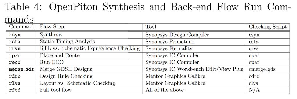
3 Whats in the Box? Synthesis Synopsys Design Compiler Static timing analysis (STA) Synopsys Primetime Formal equivalence checking (RVS) Synopsys Formality Place and route (PAR) Synopsys IC Compiler Layout versus schematic (LVS) Mentor Graphics Calibre Design rule checking (DRC) Mentor Graphics Calibre Coming soon: Gate-level simulation 3
4 Why is it Useful? Research studies Architecture, EDA, and other HW research ASIC tapeout Education 4

 1 GHz")
5 Piton ASIC 25 tiles Tested working in IBM 32nm SOI silicon! 36 mm 2 (6mm x 6mm) 1 GHz Target Frequency 5

6 Synthesis and Backend Flow 6
7 What do you need? OpenPiton Synopsys License Tools and Reference Methodology (RM) Mentor Graphics License Calibre (for LVS and DRC only) Standard cell library and process development kit 7
8 Getting Started Download Synopsys-RM Patch Synopsys-RM Familiarize with directory structure and scripts Port to process technology Running the flow 8
9 Download Synopsys-RM Synopsys Solvnet See OpenPiton Synthesis and Backend Manual Specify version Specify settings Broader support 9
10 Patching Synopsys-RM 10
11 Patching Synopsys-RM 10
12 Patching Synopsys-RM 10

13 Patching Synopsys-RM 10
14 Patching Synopsys-RM 11
15 Patching Synopsys-RM 11
16 Patching Synopsys-RM 11

17 Patching Synopsys-RM 11
18 Directory Structure and Scripts All scripts written in Tcl Two primary locations Module generic scripts Module specific scripts 12
19 Directory Structure and Scripts All scripts written in Tcl Two primary locations Module generic scripts Module specific scripts 12
20 Directory Structure and Scripts All scripts written in Tcl Two primary locations Module generic scripts Module specific scripts 12
21 Directory Structure and Scripts All scripts written in Tcl Two primary locations Module generic scripts Module specific scripts 12
22 Directory Structure and Scripts All scripts written in Tcl Two primary locations Module generic scripts Module specific scripts 12

23 Directory Structure and Scripts All scripts written in Tcl Two primary locations Module generic scripts Module specific scripts 12
24 Porting to a Process Technology ${PITON_ROOT}/piton/tools/synopsys/script/common/env_setup.tcl ${PITON_ROOT}/piton/tools/synopsys/script/common/process_setup.tcl ${PITON_ROOT}/piton/tools/calibre/script/common/calibre_ env 13

25 Porting to a Process Technology ${PITON_ROOT}/piton/tools/synopsys/script/common/env_setup.tcl ${PITON_ROOT}/piton/tools/synopsys/script/common/process_setup.tcl ${PITON_ROOT}/piton/tools/calibre/script/common/calibre_ env 13
26 Porting to a Process Technology ${PITON_ROOT}/piton/tools/synopsys/script/common/env_setup.tcl ${PITON_ROOT}/piton/tools/synopsys/script/common/process_setup.tcl ${PITON_ROOT}/piton/tools/calibre/script/common/calibre_ env 13
27 Porting to a Process Technology ${PITON_ROOT}/piton/tools/synopsys/script/common/env_setup.tcl ${PITON_ROOT}/piton/tools/synopsys/script/common/process_setup.tcl ${PITON_ROOT}/piton/tools/calibre/script/common/calibre_ env 13

28 Porting to a Process Technology ${PITON_ROOT}/piton/tools/synopsys/script/common/env_setup.tcl ${PITON_ROOT}/piton/tools/synopsys/script/common/process_setup.tcl ${PITON_ROOT}/piton/tools/calibre/script/common/calibre_ env 13
29 Porting to a Process Technology ${PITON_ROOT}/piton/tools/synopsys/script/common/env_setup.tcl ${PITON_ROOT}/piton/tools/synopsys/script/common/process_setup.tcl ${PITON_ROOT}/piton/tools/calibre/script/common/calibre_ env 13
30 Porting to a Process Technology ${PITON_ROOT}/piton/tools/synopsys/script/common/env_setup.tcl ${PITON_ROOT}/piton/tools/synopsys/script/common/process_setup.tcl ${PITON_ROOT}/piton/tools/calibre/script/common/calibre_ env 13

31 Porting to a Process Technology ${PITON_ROOT}/piton/tools/synopsys/script/common/env_setup.tcl ${PITON_ROOT}/piton/tools/synopsys/script/common/process_setup.tcl ${PITON_ROOT}/piton/tools/calibre/script/common/calibre_ env 13
32 Porting to a Process Technology 14
33 Porting to a Process Technology 14
34 Porting to a Process Technology 14
35 Porting to a Process Technology Module specific scripts suggested for review: module_setup.tcl floorplan.tcl <design_name>.constraints.tcl 15
36 Running the Flow ${PITON_ROOT}/piton/tools/synopsys/block.list 16
37 Running the Flow ${PITON_ROOT}/piton/tools/synopsys/block.list 16
38 Launch Flow 17
39 Launch Flow 17
40 Launch Flow 17
41 Launch Flow 17
42 Launch Flow 17

43 Launch Flow 17

44 Flow Runtimes 18
45 Flow Reports 19
46 Flow Outputs 20
47 Flow Outputs 20
48 Flow Outputs 20

49 Flow Outputs 20
50 Flow Outputs 21
51 Flow Outputs 21
52 Flow Outputs 21
53 Flow Outputs 21
54 Flow Outputs 21
55 Flow Outputs 21
56 Flow Outputs 21

57 Flow Outputs 21
58 Opening the Design 22
59 Opening the Design 22
60 Opening the Design 22

61 Opening the Design 22
62 Opening the Design 23

63 Opening the Design 24
64 Opening the Design 25
65 Opening the Design 26

66 Opening the Design 26

67 Opening the Design 27
Digital Systems Design
 Digital Systems Design Digital Systems Design and Test Dr. D. J. Jackson Lecture 1-1 Introduction Traditional digital design Manual process of designing and capturing circuits Schematic entry System-level
UT90nHBD Hardened-by-Design (HBD) Standard Cell Data Sheet February
 Standard Cell Data Sheet February") Semicustom Products UT90nHBD Hardened-by-Design (HBD) Standard Cell Data Sheet February 2018 www.cobham.com/hirel The most important thing we build is trust FEATURES Up to 50,000,000 2-input NAND equivalent
Semicustom Products UT90nHBD Hardened-by-Design (HBD) Standard Cell Data Sheet February 2018 www.cobham.com/hirel The most important thing we build is trust FEATURES Up to 50,000,000 2-input NAND equivalent
ASIC Computer-Aided Design Flow ELEC 5250/6250
 ASIC Computer-Aided Design Flow ELEC 5250/6250 ASIC Design Flow ASIC Design Flow DFT/BIST & ATPG Synthesis Behavioral Model VHDL/Verilog Gate-Level Netlist Verify Function Verify Function Front-End Design
Technology Timeline. Transistors ICs (General) SRAMs & DRAMs Microprocessors SPLDs CPLDs ASICs. FPGAs. The Design Warrior s Guide to.
 SRAMs & DRAMs Microprocessors SPLDs CPLDs ASICs. FPGAs. The Design Warrior s Guide to.") FPGAs 1 CMPE 415 Technology Timeline 1945 1950 1955 1960 1965 1970 1975 1980 1985 1990 1995 2000 Transistors ICs (General) SRAMs & DRAMs Microprocessors SPLDs CPLDs ASICs FPGAs The Design Warrior s Guide
FPGAs 1 CMPE 415 Technology Timeline 1945 1950 1955 1960 1965 1970 1975 1980 1985 1990 1995 2000 Transistors ICs (General) SRAMs & DRAMs Microprocessors SPLDs CPLDs ASICs FPGAs The Design Warrior s Guide
LUCEDA PHOTONICS DELIVERS A SILICON PHOTONICS IC SOLUTION IN TANNER L-EDIT
 LUCEDA PHOTONICS DELIVERS A SILICON PHOTONICS IC SOLUTION IN TANNER L-EDIT WIM BOGAERTS, PIETER DUMON, AND MARTIN FIERS, LUCEDA PHOTONICS JEFF MILLER, MENTOR GRAPHICS A M S D E S I G N & V E R I F I C
Low Power Design Methods: Design Flows and Kits
 JOINT ADVANCED STUDENT SCHOOL 2011, Moscow Low Power Design Methods: Design Flows and Kits Reported by Shushanik Karapetyan Synopsys Armenia Educational Department State Engineering University of Armenia
EE 434 Lecture 2. Basic Concepts
 EE 434 Lecture 2 Basic Concepts Review from Last Time Semiconductor Industry is One of the Largest Sectors in the World Economy and Growing All Initiatives Driven by Economic Opportunities and Limitations
CMOS VLSI IC Design. A decent understanding of all tasks required to design and fabricate a chip takes years of experience
 CMOS VLSI IC Design A decent understanding of all tasks required to design and fabricate a chip takes years of experience 1 Commonly used keywords INTEGRATED CIRCUIT (IC) many transistors on one chip VERY
Model checking in the cloud VIGYAN SINGHAL OSKI TECHNOLOGY
 Model checking in the cloud VIGYAN SINGHAL OSKI TECHNOLOGY Views are biased by Oski experience Service provider, only doing model checking Using off-the-shelf tools (Cadence, Jasper, Mentor, OneSpin Synopsys)
EE241 - Spring 2013 Advanced Digital Integrated Circuits. Projects. Groups of 3 Proposals in two weeks (2/20) Topics: Lecture 5: Transistor Models
 Topics: Lecture 5: Transistor Models") EE241 - Spring 2013 Advanced Digital Integrated Circuits Lecture 5: Transistor Models Projects Groups of 3 Proposals in two weeks (2/20) Topics: Soft errors in datapaths Soft errors in memory Integration
EE241 - Spring 2013 Advanced Digital Integrated Circuits Lecture 5: Transistor Models Projects Groups of 3 Proposals in two weeks (2/20) Topics: Soft errors in datapaths Soft errors in memory Integration
An EM-aware methodology for a high-speed multi-protocol 28Gbps SerDes design with TSMC 16FFC
 An EM-aware methodology for a high-speed multi-protocol 28Gbps SerDes design with TSMC 16FFC Bud Hunter, SerDes Analog IC Design Manager, Wipro Kelly Damalou, Sr. Technical Account Manager, Helic TSMC
Overview of Design Methodology. A Few Points Before We Start 11/4/2012. All About Handling The Complexity. Lecture 1. Put things into perspective
 Overview of Design Methodology Lecture 1 Put things into perspective ECE 156A 1 A Few Points Before We Start ECE 156A 2 All About Handling The Complexity Design and manufacturing of semiconductor products
28nm and below: New Frontiers and Innovations in Design for Manufacturing. Vito Dai, Ph.D. Sr. Member of Technical Staff, DFM
 28nm and below: New Frontiers and Innovations in Design for Manufacturing Vito Dai, Ph.D. Sr. Member of Technical Staff, DFM Outline Challenges Variability and the Limits of IC Geometrical Scaling Methodology
Low Power System-On-Chip-Design Chapter 12: Physical Libraries
 1 Low Power System-On-Chip-Design Chapter 12: Physical Libraries Friedemann Wesner 2 Outline Standard Cell Libraries Modeling of Standard Cell Libraries Isolation Cells Level Shifters Memories Power Gating
Design of Mixed-Signal Microsystems in Nanometer CMOS
 Design of Mixed-Signal Microsystems in Nanometer CMOS Carl Grace Lawrence Berkeley National Laboratory August 2, 2012 DOE BES Neutron and Photon Detector Workshop Introduction Common themes in emerging
Making your ISO Flow Flawless Establishing Confidence in Verification Tools
 Making your ISO 26262 Flow Flawless Establishing Confidence in Verification Tools Bryan Ramirez DVT Automotive Product Manager August 2015 What is Tool Confidence? Principle: If a tool supports any process
ASICs Concept to Product
 ASICs Concept to Product Synopsis This course is aimed to provide an opportunity for the participant to acquire comprehensive technical and business insight into the ASIC world. As most of these aspects
Si Photonics Technology Platform for High Speed Optical Interconnect. Peter De Dobbelaere 9/17/2012
 Si Photonics Technology Platform for High Speed Optical Interconnect Peter De Dobbelaere 9/17/2012 ECOC 2012 - Luxtera Proprietary www.luxtera.com Overview Luxtera: Introduction Silicon Photonics: Introduction
Jack Keil Wolf Lecture. ESE 570: Digital Integrated Circuits and VLSI Fundamentals. Lecture Outline. MOSFET N-Type, P-Type.
 ESE 570: Digital Integrated Circuits and VLSI Fundamentals Jack Keil Wolf Lecture Lec 3: January 24, 2019 MOS Fabrication pt. 2: Design Rules and Layout http://www.ese.upenn.edu/about-ese/events/wolf.php
High-speed low-power 2D DCT Accelerator. EECS 6321 Yuxiang Chen, Xinyi Chang, Song Wang Electrical Engineering, Columbia University Prof.
 High-speed low-power 2D DCT Accelerator EECS 6321 Yuxiang Chen, Xinyi Chang, Song Wang Electrical Engineering, Columbia University Prof. Mingoo Seok Project Goal Project Goal Execute a full VLSI design
ESE 570: Digital Integrated Circuits and VLSI Fundamentals
 ESE 570: Digital Integrated Circuits and VLSI Fundamentals Lec 3: January 24, 2019 MOS Fabrication pt. 2: Design Rules and Layout Penn ESE 570 Spring 2019 Khanna Jack Keil Wolf Lecture http://www.ese.upenn.edu/about-ese/events/wolf.php
Lessons Learned from Designing a 65 nm ASIC for Third Round SHA-3 Candidates
 Lessons Learned from Designing a 65 nm ASIC for Third Round SHA-3 Candidates Frank K. Gürkaynak, Kris Gaj, Beat Muheim, Ekawat Homsirikamol, Christoph Keller, Marcin Rogawski, Hubert Kaeslin, Jens-Peter
Fall 2017 Project Proposal
 Fall 2017 Project Proposal (Henry Thai Hoa Nguyen) Big Picture The goal of my research is to enable design automation in the field of radio frequency (RF) integrated communication circuits and systems.
Lessons Learned from Designing a 65 nm ASIC for Third Round SHA-3 Candidates
 Lessons Learned from Designing a 65 nm ASIC for Third Round SHA-3 Candidates Frank K. Gürkaynak, Kris Gaj, Beat Muheim, Ekawat Homsirikamol, Christoph Keller, Marcin Rogawski, Hubert Kaeslin, Jens-Peter
Low Power, Area Efficient FinFET Circuit Design
 Low Power, Area Efficient FinFET Circuit Design Michael C. Wang, Princeton University Abstract FinFET, which is a double-gate field effect transistor (DGFET), is more versatile than traditional single-gate
Low Power Radiation Tolerant CMOS Design using Commercial Fabrication Processes
 Low Power Radiation Tolerant CMOS Design using Commercial Fabrication Processes Amir Hasanbegovic (amirh@ifi.uio.no) Nanoelectronics Group, Dept. of Informatics, University of Oslo November 5, 2010 Overview
Agenda. 9:30 Registration & Coffee Networking and Sponsor Table-tops Welcome and introduction
 Agenda 9:30 Registration & Coffee Networking and Sponsor Table-tops 10.00 Welcome and introduction Break 12:45 Lunch Break Flexible debug and visibility techniques to enhance all FPGA design and deployment
Course Outcome of M.Tech (VLSI Design)
") Course Outcome of M.Tech (VLSI Design) PVL108: Device Physics and Technology The students are able to: 1. Understand the basic physics of semiconductor devices and the basics theory of PN junction. 2.
Course Outcome of M.Tech (VLSI Design) PVL108: Device Physics and Technology The students are able to: 1. Understand the basic physics of semiconductor devices and the basics theory of PN junction. 2.
DATASHEET CADENCE QRC EXTRACTION
 DATASHEET Cadence QRC Etraction, the industry s premier 3D fullchip parasitic etractor that is independent of design style or flow, is a fast and accurate RLCK etraction solution used during design implementation
SpringerBriefs in Electrical and Computer Engineering
 SpringerBriefs in Electrical and Computer Engineering For further volumes: http://www.springer.com/series/10059 Vikram Arkalgud Chandrasetty VLSI Design A Practical Guide for FPGA and ASIC Implementations
Lecture 1: Introduction to Digital System Design & Co-Design
 Design & Co-design of Embedded Systems Lecture 1: Introduction to Digital System Design & Co-Design Computer Engineering Dept. Sharif University of Technology Winter-Spring 2008 Mehdi Modarressi Topics
Mixed Signal Virtual Components COLINE, a case study
 Mixed Signal Virtual Components COLINE, a case study J.F. POLLET - DOLPHIN INTEGRATION Meylan - FRANCE http://www.dolphin.fr Overview of the presentation Introduction COLINE, an example of Mixed Signal
Low Power, Radiation tolerant microelectronics design techniques. Executive Summary REF : ASP-04-BO/PE-476 DATE : 02/11/2004 ISSUE : -/2 PAGE : 1 /18
 ISSUE : -/2 PAGE : 1 /18 Executive Summary Written by Responsibility-Company Date Signature Project team Alcatel Space and Imec Verified by Emmanuel Liegeon ASIC Design Engineer - Study responsible Approved
Innovations in EDA Webcast Series
 Welcome Innovations in EDA Webcast Series August 2, 2012 Jack Sifri MMIC Design Flow Specialist IC, Laminate, Package Multi-Technology PA Module Design Methodology Realizing the Multi-Technology Vision
Digital IC-Project and Verification
 Digital IC-Project and Verification (STA) Liang Liu & Joachim Rodrigues Outline STA & PrimeTime Overview STA Using PrimeTime Basic Concepts PrimeTime Flow Suggestions What s STA STA is a method of validating
Lecture 3, Handouts Page 1. Introduction. EECE 353: Digital Systems Design Lecture 3: Digital Design Flows, Simulation Techniques.
 Introduction EECE 353: Digital Systems Design Lecture 3: Digital Design Flows, Techniques Cristian Grecu grecuc@ece.ubc.ca Course web site: http://courses.ece.ubc.ca/353/ What have you learned so far?
1. Introduction. Institute of Microelectronic Systems. Status of Microelectronics Technology. (nm) Core voltage (V) Gate oxide thickness t OX
 Core voltage (V) Gate oxide thickness t OX") Threshold voltage Vt (V) and power supply (V) 1. Introduction Status of s Technology 10 5 2 1 0.5 0.2 0.1 V dd V t t OX 50 20 10 5 2 Gate oxide thickness t OX (nm) Future VLSI chip 2005 2011 CMOS feature
Threshold voltage Vt (V) and power supply (V) 1. Introduction Status of s Technology 10 5 2 1 0.5 0.2 0.1 V dd V t t OX 50 20 10 5 2 Gate oxide thickness t OX (nm) Future VLSI chip 2005 2011 CMOS feature
Lecture 1. Tinoosh Mohsenin
 Lecture 1 Tinoosh Mohsenin Today Administrative items Syllabus and course overview Digital systems and optimization overview 2 Course Communication Email Urgent announcements Web page http://www.csee.umbc.edu/~tinoosh/cmpe650/
Formal Hardware Verification: Theory Meets Practice
 Formal Hardware Verification: Theory Meets Practice Dr. Carl Seger Senior Principal Engineer Tools, Flows and Method Group Server Division Intel Corp. June 24, 2015 1 Quiz 1 Small Numbers Order the following
Introduction to Virtuoso & Calibre
 Introduction to Virtuoso & Calibre Courtesy of Dr. Harris @HMC, and Dr. Choi @PSU http://csce.uark.edu +1 (479) 575-6043 yrpeng@uark.edu Process Design Kit (PDK) The manufacturing grid defines the minimum
AN EFFICIENT APPROACH TO MINIMIZE POWER AND AREA IN CARRY SELECT ADDER USING BINARY TO EXCESS ONE CONVERTER
 AN EFFICIENT APPROACH TO MINIMIZE POWER AND AREA IN CARRY SELECT ADDER USING BINARY TO EXCESS ONE CONVERTER K. RAMAMOORTHY 1 T. CHELLADURAI 2 V. MANIKANDAN 3 1 Department of Electronics and Communication
ISSN:
 1391 DESIGN OF 9 BIT SAR ADC USING HIGH SPEED AND HIGH RESOLUTION OPEN LOOP CMOS COMPARATOR IN 180NM TECHNOLOGY WITH R-2R DAC TOPOLOGY AKHIL A 1, SUNIL JACOB 2 1 M.Tech Student, 2 Associate Professor,
BITSTACKING WITH ONLY A COMPOSER SCHEMATIC EDITOR LICENSE TONY LAUNDRIE IC DESIGN ENGINEER. P.O. BOX 4000 CHIPPEWA FALLS, WI
 BITSTACKING WITH ONLY A COMPOSER SCHEMATIC EDITOR LICENSE TONY LAUNDRIE IC DESIGN ENGINEER P.O. BOX 4000 CHIPPEWA FALLS, WI 54729 atl@sgi.com INTERNATIONAL CADENCE USER GROUP CONFERENCE SEPTEMBER 10-13,
CHAPTER 1 INTRODUCTION
 CHAPTER 1 INTRODUCTION 1.1 Historical Background Recent advances in Very Large Scale Integration (VLSI) technologies have made possible the realization of complete systems on a single chip. Since complete
Design of digital cmos circuits by Using Standard Cell Library for high performance
 ISSN: 2278 1323 All Rights Reserved 2014 IJARCET 3564 International Journal of Advanced Research in Computer Engineering & (IJARCET) Design of digital cmos circuits by Using Standard Cell Library for high
Design, Optimization and Production of an Ultra-Wideband (UWB) Receiver
 Receiver") Application Note Design, Optimization and Production of an Ultra-Wideband (UWB) Receiver Overview This application note describes the design process for an ultra-wideband (UWB) receiver, including both
Application Note Design, Optimization and Production of an Ultra-Wideband (UWB) Receiver Overview This application note describes the design process for an ultra-wideband (UWB) receiver, including both
MHz phase-locked loop
 SPECIFICATION 1 FEATURES 50 800 MHz phase-locked loop TSMC CMOS 65 nm Output frequency from 50 to 800 MHz Reference frequency from 4 to 30 MHz Power supply 1.2 V CMOS output Supported foundries: TSMC,
IC Layout Design of 4-bit Universal Shift Register using Electric VLSI Design System
 IC Layout Design of 4-bit Universal Shift Register using Electric VLSI Design System 1 Raj Kumar Mistri, 2 Rahul Ranjan, 1,2 Assistant Professor, RTC Institute of Technology, Anandi, Ranchi, Jharkhand,
EE 434 ASIC & Digital Systems
 EE 434 ASIC & Digital Systems Dae Hyun Kim EECS Washington State University Spring 2017 Course Website http://eecs.wsu.edu/~ee434 Themes Study how to design, analyze, and test a complex applicationspecific
Hot Topics and Cool Ideas in Scaled CMOS Analog Design
 Engineering Insights 2006 Hot Topics and Cool Ideas in Scaled CMOS Analog Design C. Patrick Yue ECE, UCSB October 27, 2006 Slide 1 Our Research Focus High-speed analog and RF circuits Device modeling,
Lecture 4&5 CMOS Circuits
 Lecture 4&5 CMOS Circuits Xuan Silvia Zhang Washington University in St. Louis http://classes.engineering.wustl.edu/ese566/ Worst-Case V OL 2 3 Outline Combinational Logic (Delay Analysis) Sequential Circuits
Timing analysis can be done right after synthesis. But it can only be accurately done when layout is available
 Timing Analysis Lecture 9 ECE 156A-B 1 General Timing analysis can be done right after synthesis But it can only be accurately done when layout is available Timing analysis at an early stage is not accurate
Ramon Canal NCD Master MIRI. NCD Master MIRI 1
 Wattch, Hotspot, Hotleakage, McPAT http://www.eecs.harvard.edu/~dbrooks/wattch-form.html http://lava.cs.virginia.edu/hotspot http://lava.cs.virginia.edu/hotleakage http://www.hpl.hp.com/research/mcpat/
EEC 116 Fall 2011 Lab #2: Analog Simulation Tutorial
 EEC 116 Fall 2011 Lab #2: Analog Simulation Tutorial Dept. of Electrical and Computer Engineering University of California, Davis Issued: September 28, 2011 Due: October 12, 2011, 4PM Reading: Rabaey Chapters
Advanced FPGA Design. Tinoosh Mohsenin CMPE 491/691 Spring 2012
 Advanced FPGA Design Tinoosh Mohsenin CMPE 491/691 Spring 2012 Today Administrative items Syllabus and course overview Digital signal processing overview 2 Course Communication Email Urgent announcements
Challenges in Transition
 Challenges in Transition Keynote talk at International Workshop on Software Engineering Methods for Parallel and High Performance Applications (SEM4HPC 2016) 1 Kazuaki Ishizaki IBM Research Tokyo kiszk@acm.org
Advanced Techniques for Using ARM's Power Management Kit
 ARM Connected Community Technical Symposium Advanced Techniques for Using ARM's Power Management Kit Libo Chang( 常骊波 ) ARM China 2006 年 12 月 4/6/8 日, 上海 / 北京 / 深圳 Power is Out of Control! Up to 90nm redu
A fully synthesizable injection-locked PLL with feedback current output DAC in 28 nm FDSOI
 LETTER IEICE Electronics Express, Vol.1, No.15, 1 11 A fully synthesizable injection-locked PLL with feedback current output DAC in 8 nm FDSOI Dongsheng Yang a), Wei Deng, Aravind Tharayil Narayanan, Rui
Amber Path FX SPICE Accurate Statistical Timing for 40nm and Below Traditional Sign-Off Wastes 20% of the Timing Margin at 40nm
 Amber Path FX SPICE Accurate Statistical Timing for 40nm and Below Amber Path FX is a trusted analysis solution for designers trying to close on power, performance, yield and area in 40 nanometer processes
NanoFabrics: : Spatial Computing Using Molecular Electronics
 NanoFabrics: : Spatial Computing Using Molecular Electronics Seth Copen Goldstein and Mihai Budiu Computer Architecture, 2001. Proceedings. 28th Annual International Symposium on 30 June-4 4 July 2001
A Top-Down Microsystems Design Methodology and Associated Challenges
 A Top-Down Microsystems Design Methodology and Associated Challenges Michael S. McCorquodale, Fadi H. Gebara, Keith L. Kraver, Eric D. Marsman, Robert M. Senger, and Richard B. Brown Department of Electrical
LOW POWER SCANNER FOR HIGH-DENSITY ELECTRODE ARRAY NEURAL RECORDING
 LOW POWER SCANNER FOR HIGH-DENSITY ELECTRODE ARRAY NEURAL RECORDING A Thesis work submitted to the faculty of San Francisco State University In Partial Fulfillment of the Requirements for the Degree Master
F O U N D R Y L E A D E R S H I P F O R T H E S o C G E N E R A T I O N. 90 Nanometer.
 F O U N D R Y L E A D E R S H I P F O R T H E S o C G E N E R A T I O N 90 Nanometer 90 www.umc.com 90 Nanometer UMC has been shipping customer products based on its 90-nanometer (0.09-um) logic process
Basic FPGA Tutorial. using VHDL and VIVADO to design two frequencies PWM modulator system
 Basic FPGA Tutorial using VHDL and VIVADO to design two frequencies PWM modulator system January 30, 2018 Contents 1 INTRODUCTION........................................... 1 1.1 Motivation................................................
REVOLUTIONIZING THE COMPUTING LANDSCAPE AND BEYOND.
 December 3-6, 2018 Santa Clara Convention Center CA, USA REVOLUTIONIZING THE COMPUTING LANDSCAPE AND BEYOND. https://tmt.knect365.com/risc-v-summit @risc_v ACCELERATING INFERENCING ON THE EDGE WITH RISC-V
CMOS Technology for Computer Architects
 CMOS Technology for Computer Architects Lecture 1: Introduction Iakovos Mavroidis Giorgos Passas Manolis Katevenis FORTH-ICS (University of Crete) Course Contents Implementation of high-performance digital
! Review: MOS IV Curves and Switch Model. ! MOS Device Layout. ! Inverter Layout. ! Gate Layout and Stick Diagrams. ! Design Rules. !
 ESE 570: Digital Integrated Circuits and VLSI Fundamentals Lec 3: January 21, 2017 MOS Fabrication pt. 2: Design Rules and Layout Lecture Outline! Review: MOS IV Curves and Switch Model! MOS Device Layout!
Advanced In-Design Auto-Fixing Flow for Cell Abutment Pattern Matching Weakpoints
 Cell Abutment Pattern Matching Weakpoints Yongfu Li, Valerio Perez, I-Lun Tseng, Zhao Chuan Lee, Vikas Tripathi, Jason Khaw and Yoong Seang Jonathan Ong GLOBALFOUNDRIES Singapore ABSTRACT Pattern matching
ICE of silicon. [Roza] Computational efficiency [MOPS/W] 3DTV. Intrinsic computational efficiency.
![ICE of silicon. [Roza] Computational efficiency [MOPS/W] 3DTV. Intrinsic computational efficiency.](/thumbs/78/77184694.jpg "ICE of silicon. [Roza] Computational efficiency [MOPS/W] 3DTV. Intrinsic computational efficiency.") SoC Design ICE of silicon Computational efficiency [MOPS/W] 10 6 [Roza] 10 5 Intrinsic computational efficiency 3DTV 10 4 10 3 10 2 10 1 i386sx 601 604 604e microsparc Ultra sparc i486dx P5 Super sparc
SoC Design ICE of silicon Computational efficiency [MOPS/W] 10 6 [Roza] 10 5 Intrinsic computational efficiency 3DTV 10 4 10 3 10 2 10 1 i386sx 601 604 604e microsparc Ultra sparc i486dx P5 Super sparc
--- An integrated 3D EM design flow for EM/Circuit Co-Design
 ADS users group meeting 2009 Rome 13/05, Böblingen 14-15/05, Massy 16/06 --- An integrated 3D EM design flow for EM/Circuit Co-Design Motivations and drivers for co-design Throw-The-Die-Over-The-Wall,
! Review: MOS IV Curves and Switch Model. ! MOS Device Layout. ! Inverter Layout. ! Gate Layout and Stick Diagrams. ! Design Rules. !
 ESE 570: Digital Integrated Circuits and VLSI Fundamentals Lec 3: January 21, 2016 MOS Fabrication pt. 2: Design Rules and Layout Lecture Outline! Review: MOS IV Curves and Switch Model! MOS Device Layout!
ESE 570: Digital Integrated Circuits and VLSI Fundamentals
 ESE 570: Digital Integrated Circuits and VLSI Fundamentals Lec 3: January 21, 2016 MOS Fabrication pt. 2: Design Rules and Layout Penn ESE 570 Spring 2016 Khanna Adapted from GATech ESE3060 Slides Lecture
An Efficient Design of CMOS based Differential LC and VCO for ISM and WI-FI Band of Applications
 IJSTE - International Journal of Science Technology & Engineering Volume 2 Issue 10 April 2016 ISSN (online): 2349-784X An Efficient Design of CMOS based Differential LC and VCO for ISM and WI-FI Band
RTL Power Estimation Flow and Its Use in Power Optimization
 RTL Power Estimation Flow and Its Use in Power Optimization Sondre Rennan Nesset Master of Science in Electronics Submission date: June 2018 Supervisor: Per Gunnar Kjeldsberg, IES Co-supervisor: Knut Austbø,
EECS150 - Digital Design Lecture 28 Course Wrap Up. Recap 1
 EECS150 - Digital Design Lecture 28 Course Wrap Up Dec. 5, 2013 Prof. Ronald Fearing Electrical Engineering and Computer Sciences University of California, Berkeley (slides courtesy of Prof. John Wawrzynek)
CS250 VLSI Systems Design. Lecture 3: Physical Realities: Beneath the Digital Abstraction, Part 1: Timing
 CS250 VLSI Systems Design Lecture 3: Physical Realities: Beneath the Digital Abstraction, Part 1: Timing Fall 2010 Krste Asanovic, John Wawrzynek with John Lazzaro and Yunsup Lee (TA) What do Computer
ECE Digital VLSI Design Course Syllabus Fall 2017
 ECE484-001 Digital VLSI Design Course Syllabus Fall 2017 Instructor: Dr. George L. Engel Phone: (618) 650-2806 Office: Email: URLs: Engineering Building Room EB3043 gengel@siue.edu http://www.siue.edu/~gengel
RFIC Design ELEN 376 Session 1
 RFIC Design ELEN 376 Session 1 Instructor: Dr. Allen Sweet April 3, 2002 Copy right 2002, elen376 1 General Information Instructor: Dr. Allen Sweet Email: allensweet@aol.com Home work/project submissions:
RFIC Design ELEN 351 Lecture 1: General Discussion
 RFIC Design ELEN 351 Lecture 1: General Discussion Instructor: Dr. Allen Sweet Copy right 2003, ELEN351 1 General Information Instructor: Dr. Allen Sweet Email: allensweet@aol.com Home work/project submissions:
The backend duplication method
 The backend duplication method - A Leakage-Proof Place-and and-route Strategy for Secured ASICs - CHES Workshop August 30th September 1st 2005 Edinburgh, Scotland, UK. Sylvain GUILLEY (*), Philippe HOOGVORST
3-2-1 Contact: An Experimental Approach to the Analysis of Contacts in 45 nm and Below. Rasit Onur Topaloglu, Ph.D.
 3-2-1 Contact: An Experimental Approach to the Analysis of Contacts in 45 nm and Below Rasit Onur Topaloglu, Ph.D. Outline Introduction and Motivation Impact of Contact Resistance Test Structures for Contact
The Physical Design of Long Time Delay-chip
 2011 International Conference on Computer Science and Information Technology (ICCSIT 2011) IPCSIT vol. 51 (2012) (2012) IACSIT Press, Singapore DOI: 10.7763/IPCSIT.2012.V51.137 The Physical Design of Long
ERAU the FAA Research CEH Tools Qualification
 ERAU the FAA Research 2007-2009 CEH Tools Qualification Contract DTFACT-07-C-00010 Dr. Andrew J. Kornecki, Dr. Brian Butka Embry Riddle Aeronautical University Dr. Janusz Zalewski Florida Gulf Coast University
XI μm Process Family: The XI10 series is X-Fab's 1.0-micron Modular Silicon-On-Insulator Technology DESCRIPTION
 1.0 μm Process Family: XI10 The XI10 series is X-Fab's 1.0-micron Modular Silicon-On-Insulator Technology DESCRIPTION The XI10 series is X-FAB s 1.0 micron Modular Non-fully Depleted SOI CMOS Technology.
Digital Signal Processing for an Integrated Power-Meter
 49. Internationales Wissenschaftliches Kolloquium Technische Universität Ilmenau 27.-30. September 2004 Borisav Jovanović / Milunka Damnjanović / Predrag Petković Digital Signal Processing for an Integrated
Technology Transfers Opportunities, Process and Risk Mitigation. Radhika Srinivasan, Ph.D. IBM
 Technology Transfers Opportunities, Process and Risk Mitigation Radhika Srinivasan, Ph.D. IBM Abstract Technology Transfer is quintessential to any technology installation or semiconductor fab bring up.
Analog Custom Layout Engineer
 Analog Custom Layout Engineer Huawei Canada s rapid growth has created an excellent opportunity to build and grow your career and make a big impact to everyone s life. The IC Lab is currently looking to
DIGITAL IMPLEMENTATION OF HIGH SPEED PULSE SHAPING FILTERS AND ADDRESS BASED SERIAL PERIPHERAL INTERFACE DESIGN
 DIGITAL IMPLEMENTATION OF HIGH SPEED PULSE SHAPING FILTERS AND ADDRESS BASED SERIAL PERIPHERAL INTERFACE DESIGN A Thesis Presented to The Academic Faculty by Arun Rachamadugu In Partial Fulfillment of
Agenda. 9:30 Registration & Coffee Networking and Sponsor Table-tops Welcome and introduction
 Agenda 9:30 Registration & Coffee Networking and Sponsor Table-tops 10.00 Welcome and introduction Break 12:30 Lunch Break Flexible debug and visibility techniques to enhance all FPGA design and deployment
F O U N D R Y L E A D E R S H I P F O R T H E S o C G E N E R A T I O N. 65 Nanometer.
 F O U N D R Y L E A D E R S H I P F O R T H E S o C G E N E R A T I O N 65 Nanometer 65 www.umc.com 65 Nanometer UMC is the foundry leader in 65nm process technology, having delivered the foundry industry
Power-Delivery Network in 3D ICs: Monolithic 3D vs. Skybridge 3D CMOS
 -Delivery Network in 3D ICs: Monolithic 3D vs. Skybridge 3D CMOS Jiajun Shi, Mingyu Li and Csaba Andras Moritz Department of Electrical and Computer Engineering University of Massachusetts, Amherst, MA,
CMOS Digital Logic Design with Verilog. Chapter1 Digital IC Design &Technology
 CMOS Digital Logic Design with Verilog Chapter1 Digital IC Design &Technology Chapter Overview: In this chapter we study the concept of digital hardware design & technology. This chapter deals the standard
EC 1354-Principles of VLSI Design
 EC 1354-Principles of VLSI Design UNIT I MOS TRANSISTOR THEORY AND PROCESS TECHNOLOGY PART-A 1. What are the four generations of integrated circuits? 2. Give the advantages of IC. 3. Give the variety of
Design of low-loss 60 GHz integrated antenna switch in 65 nm CMOS
 LETTER IEICE Electronics Express, Vol.15, No.7, 1 10 Design of low-loss 60 GHz integrated antenna switch in 65 nm CMOS Korkut Kaan Tokgoz a), Seitaro Kawai, Kenichi Okada, and Akira Matsuzawa Department
In 1951 William Shockley developed the world first junction transistor. One year later Geoffrey W. A. Dummer published the concept of the integrated
 Objectives History and road map of integrated circuits Application specific integrated circuits Design flow and tasks Electric design automation tools ASIC project MSDAP In 1951 William Shockley developed
E SC 521 Pattern Generation at the Nanoscale Wook Jun Nam The Pennsylvania State University
 E SC 521 Pattern Generation at the Nanoscale Wook Jun Nam Unit 1 Lithography General Information Lecture 2B Layout Design II Outline Layout Design Define Function Design Partition Design Simulation Typical
SiGe BiCMOS Technologies with RF and Photonic Modules
 INNOVATIONS FOR HIGH PERFORMANCE MICROELECTRONICS SiGe BiCMOS Technologies with RF and Photonic Modules Mul Project and Low Volume Wafer Produc on About Us IHP-GmbH is a German R & D institution, focused
Layout - Line of Diffusion. Where are we? Line of Diffusion in General. Line of Diffusion in General. Stick Diagrams. Line of Diffusion in General
 Where are we? Lots of Layout issues Line of diffusion style Power pitch it-slice pitch Routing strategies Transistor sizing Wire sizing Layout - Line of Diffusion Very common layout method Start with a
An Example Design using the Analog Photonics Component Library. 3/21/2017 Benjamin Moss
 An Example Design using the Analog Photonics Component Library 3/21/2017 Benjamin Moss Component Library Elements Passive Library Elements: Component Current specs 1 Edge Couplers (Si)
Reducing Development Risk in Communications Applications with High-Performance Oscillators
 V.7/17 Reducing Development Risk in Communications Applications with High-Performance Oscillators Introducing Silicon Labs new Ultra Series TM Oscillators Powered by 4 th Generation DSPLL Technology, new