Optical waveguides in crystalline dielectric materials produced by femtosecond-laser micromachining
|
|
|
- Emily Florence Byrd
- 5 years ago
- Views:
Transcription


1 lpor frontispiece.indd 1 13/02/14 6:32 AM
 has been developed as one of the most efficient techniques for direct")
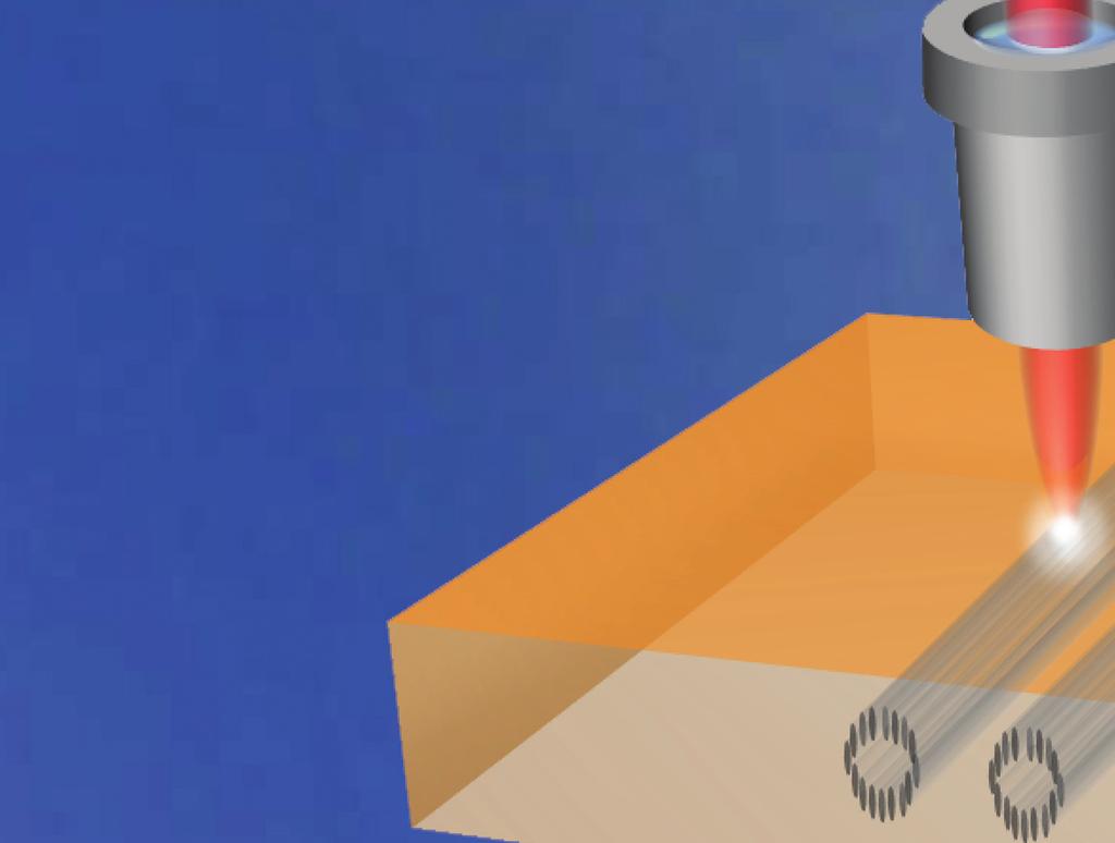
2 Laser Photonics Rev. 8, No. 2, (2014) / DOI /lpor LASER & PHOTONICS REVIEWS Abstract Femtosecond-laser micromachining (also known as inscription or writing) has been developed as one of the most efficient techniques for direct three-dimensional microfabrication of transparent optical materials. In integrated photonics, by using direct writing of femtosecond/ultrafast laser pulses, optical waveguides can be produced in a wide variety of optical materials. With diverse parameters, the formed waveguides may possess different configurations. This paper focuses on crystalline dielectric materials, and is a review of the state-of-the-art in the fabrication, characterization and applications of femtosecondlaser micromachined waveguiding structures in optical crystals and ceramics. A brief outlook is presented by focusing on a few potential spotlights. REVIEW ARTICLE Optical waveguides in crystalline dielectric materials produced by femtosecond-laser micromachining Feng Chen 1, and J. R. Vázquez de Aldana 2 1. Introduction In integrated photonics, optical waveguides are basic components that are defined as high refractive index cores surrounded by low-index layers. Generally, the waveguide structures have very small volumes, in which the light intensities reach very high levels owing to the tight confinement of the light fields in the refractive-index constructed potential wells [1, 2]. Benefiting from the compact geometry of the structures, the functional guiding devices may be manufactured on chip-scale wafers, by which integrated photonic circuits may be fabricated for diverse applications [3 6]. In addition, some features (e.g., lasing performances, nonlinear responses, etc.) might be enhanced to a certain extent in the waveguides with respect to the bulks, enabling the realization of highly efficient miniaturized platforms for a number of applications for photonic signal processing [7 10]. Waveguides in diverse configurations can be fabricated by a few developed techniques, including metal-ion indiffusion [11], ion/proton exchange [8, 12], epitaxial layer deposition (sputtering, molecular beam epitaxy (MBE), chemical vapor deposition (CVD), pulsed laser deposition (PLD), etc.) [13, 14], ion-beam implantation/irradiation [15 17], and femtosecond (fs) laser micromachining/writing [18]. Fs-laser micromachining has recently emerged as one of the most efficient techniques for direct three-dimensional microfabrication of transparent optical materials [18 27]. The energy of the fs pulses is absorbed through nonlinear process (i.e. two-photon or multiphoton absorption), inducing avalanche ionization in a very short time that does not allow the fast heat-transfer process [18]. Because of this feature, focused fs-laser pulses produce localized modifications of micro or submicrometric scales in the focal volume inside the material, in which permanent or very stable refractive-index changes may be created. Since 1996, the first report on fs-laser written waveguides in a few family glasses was presented by Davis et al. [28], numerous subsequent works have been performed towards waveguide fabrication in various transparent materials [29 37]. It has been found that the refractive-index modifications in the fs-laser-irradiated regions could be either positive or negative, depending on the nature of the materials as well as on the parameters of the applied fs-laser pulses. In addition, high-energy fs-laser pulses are used to ablate transparent dielectrics in micrometric scales. With suitable engineering of the refractive index in the special local regions inside the materials, one can produce various photonic structures, such as optical waveguides, photonic crystals, diffractive gratings, etc., in a direct procedure without using patterned masking [30]. With different parameters, the fs-laser micromachined waveguides may possess different configurations, supporting diverse guidance along different axes. More importantly, as a direct technique for waveguide fabrication, the fs-laser micromachining (mostly by inscribing 1 School of Physics, State Key Laboratory of Crystal Materials, and Key Laboratory of Particle Physics and Particle Irradiation, Ministry of Education, Shandong University, Jinan , China 2 Laser Microprocessing Group, Facultad de Ciencias, Universidad de Salamanca, Salamanca 37008, Spain Corresponding author: drfchen@sdu.edu.cn
3 LASER & PHOTONICS REVIEWS 252 F. Chen and J. R. Vázquez de Aldana: Optical waveguides in crystalline dielectric materials index-changed filaments) has shown wide applicability in a large number of materials, including amorphous glasses, single crystals, polycrystalline ceramics, organic polymers, etc. [29 37]. Optical dielectric crystals are important materials for many aspects of modern life [38 40]. For example, electrooptic crystals are ideal platforms for the modulation of light phase, energy and polarizations. Nonlinear crystals are important frequency converters of light from different wavelength regions. Laser crystals are the favorite gain media for solid-state laser systems with lower lasing thresholds than glasses. Based on dielectric crystals, various optical applications can be realized through a broad variety of devices and components. With the combination of compact geometry of waveguides and useful features of crystals, crystalline waveguides become unique platforms for versatile photonic applications. As of yet, numerous works have been performed world-wide on fs-laser micromachined waveguides in various glasses, forming key components in photonic devices such as microfluidic chips [29, 41], all-optical routers or switches [42], continuous-wave (cw) or pulsed integrated laser sources [43 46], amplifiers [47 49], and quantum photonic devices [50]. On the contrary, crystalline waveguides received considerable attention until more recently. Nevertheless, a number of new waveguides have been fabricated in crystals and some applications based on the crystalline waveguides are very exciting. In addition, fs-laser micromachined guiding structures can be fabricated with multiple configurations, which offer diverse options to realize versatile applications. In this work, we focus on the up-to-date progress on the optical waveguides in dielectric crystals fabricated by fs-laser micromachining. Heinrich et al. presented a simple review on this topic but most new results were missing due to the very rapid development of the research field undergone recently [51]. In our work, the fundamentals of the fs-laser interaction with the crystal materials are briefly demonstrated in Section 2. The fabrication of diverse waveguide configurations by fs-laser micromachining is introduced in Section 3. Section 4 focuses on the applied crystal materials and their properties, giving a state-of-the-art overview of the reported literatures. In Section 5, selected applications of fs-laser fabricated crystalline waveguides are presented. An outlook with summary will be given in Section Fundamentals on microprocessing of crystals with femtosecond laser pulses 2.1. Interaction of dielectrics with intense femtosecond pulses The fs-laser irradiation is nowadays consolidated as a very powerful technique for the microprocessing of transparent dielectrics [18,21], both in the surface and in the bulk. The great interest of using such laser sources, instead of longerpulse lasers (nanosecond, ns) or other techniques, for highprecision materials processing is that micromodifications can be produced in a very small region of the sample, while reducing the surrounding affected area at minimum [52]. The reason for that is the extremely short temporal scale of the laser matter interaction: at the time the laser pulse is over, the thermal coupling of electrons and ions is negligible [53]. Most of the crystals interesting for photonic applications are transparent to the near-infrared wavelengths of the usual ultrashort pulse lasers (i.e. Ti:sapphire at 800 nm or Yb-doped fiber laser at 1.04 μm), due to the large bandgap of such materials [54]. When an intense ultrashort laser pulse is focused in the surface of a transparent dielectric, a number of electrons will be detached from their parent atoms [55] through the so-called processes of strong-field ionization [56]: multiphoton or tunnel ionization. There exists no threshold intensity for such processes to take place, but in order to get a significant number of free electrons, intensities in the range of W/cm 2 are usually required. The free electrons that are generated continue their interaction with the laser pulse, absorbing more energy by inverse Bremsstrahlung, and colliding with other bound electrons that will be released (a process known as avalanche ionization). As a result, after the irradiation with an intense femtosecond pulse, the exposed material consists of a hot and dense electronic plasma, and a lattice of ions. The processes subsequent to the laser interaction are very complex [57] and will depend strongly on the material and on the laser parameters. In general, if the laser intensity is large enough to produce a plasma density exceeding some critical value, a process known as ultrafast ablation [58] will take place by Coulomb explosion (electrons and ions ejection) giving rise to the creation of a shallow crater (nanometer scale [59]) in the material surface, with minimal thermal affection to the surrounding material. Laser fluences of a few J/cm 2 are required to produce ablation with IR femtosecond pulses. The irradiation of the sample with multiple femtosecond pulses leads to the formation of a deeper ablation crater when the laser beam is focused at the same spot or to an ablation groove if the sample is moved at a certain velocity while irradiating. These techniques have been successfully used for the precise surface microstructuring of crystals, thus enabling the fabrication of photonic devices. For instance, the integration of diffractive patterns (relief gratings) for beam-shaping applications has been explored in laser [60] and nonlinear [61 64] crystals. Concerning the inscription of optical waveguides in crystals by ultrafast ablation, two approaches have been demonstrated. On the one hand, under certain conditions, the shock wave generated in the unprocessed material due to the ablation mechanism, results in a local refractive-index increase. This can be used for the fabrication of a waveguides by simply producing an ablation groove along the surface of a crystal [65]. On the other hand, ultrafast ablation has also been used for the inscription of ridge waveguides [66] in ion-implanted crystals [15]: the procedure consists of micromachining two parallel ablation grooves along the sample that keep the light confined transversally thus shaping the waveguide mode.
4 REVIEW ARTICLE Laser Photonics Rev. 8, No. 2 (2014) 253 The process of laser matter interaction at high intensities is even more complex when the laser pulse is focused at some depth inside the transparent dielectric [29], provided that the pulse will undergo also nonlinear propagation [67] thus modifying the intensity distribution from that expected in a linear (low-intensity) regime. The mechanisms affecting the pulse propagation are mainly related to the third-order nonlinear susceptibility and the optical Kerr effect, giving rise to a very complex dynamics. For large pulse powers, the beam will experience self-focusing [68], thus contributing to a further increase in the local onaxis intensity. Then, as the pulse propagates towards the focus, strong-field ionization takes place and the plasma that is generated tends to defocus the beam and absorbs energy from the pulse at the same time. The opposed effects of self-focusing and plasma generation (defocusing) sometimes produces a dynamic light channel in which the beam propagates concentrated at a very small size for a distance of several Rayleigh lengths of the focusing beam: the process is named filamentation [69]. It is well accepted that the laser-created plasma is the origin of the modifications that will take place in the focal volume [70] after the interaction with the laser pulse. However, the physical mechanisms that take place after the free-electron plasma has transferred its energy to the lattice, are not fully understood yet [29] Micromodifications of crystals with femtosecond pulses The observed morphological changes induced by the irradiation of crystals with femtosecond pulses can be classified mainly in two groups [71]. The first one consists of producing a weak damage at the focal volume that leads to a smooth modification (positive) of the refractive index in this region. The crystal in which such a modification was first observed was LiNbO 3 [72] and its formation is linked to the creation of point defects at the focal volume that lower the spontaneous polarization of the crystal [73]. Fabrication of optical waveguides by this procedure is direct and simple (as will be discussed in Section 3) just by scanning the sample, has been demonstrated in a vast number of glasses. However, such waveguides in crystals have the main drawback that they can be strongly deteriorated or even removed completely by heating the sample. As of yet, it has been observed only in a few crystalline materials, such as LiNbO 3 [71, 72, 74], ZnSe [75] and Nd:YCa 4 O(BO 3 ) 3 [76]. It can be explained because a refractive-index increase typically requires an increase in the material density, and this is something difficult to achieve in materials with crystalline structure due to the large natural positional order of the lattice. The other group of morphological changes consists of the generation of a severe damage track along the propagation direction in a more or less long volume around the nonlinear laser focus. It has been reported in a number of crystals (Nd:YAG, LiNbO 3, Nd:GGG, Nd:YVO 4... ) that the refractive index at the damage tracks decreases with respect to that of the bulk [77], which typically corresponds to a local amorphization of the material [78]. Additionally, a stress field is created at the surrounding material leading to a refractive-index increase [73] that can be used for waveguide fabrication. Spectroscopic studies, e.g., microphotoluminescence (μ-pl) or micro-raman (μ-raman), performed in rare-earth-doped crystals or polycrystalline materials (ceramics) have provided much information on the particular microstructural modifications that take place at the damage tracks and in the surroundings. Although the response of the material to the laser irradiation depends on the particular crystal used, the following observations [79] performed in a Nd:YAG ceramic, are quite general: a) irreversible lattice damage at the core of the tracks, associated with the creation of a continuous line of submicrometer-sized amorphous damage voxels, b) compressed crystalline material in the vicinity of the filaments core, with a high density of thermally removable defects and lattice imperfections, and c) compressed crystalline material in the surroundings of the tracks, which is thermally stable. As an example, in Fig. 1a we show the damage tracks produced in a Nd:GGG crystal with 120-fs pulses at 1 khz repetition rate and a large pulse energy of 5.8 μj [80]. The microluminescence analysis of the 4 F 3/2 4 I 9/2 emission line (933 nm) of Nd 3+ ions (Figs. 1b e) reveals a clear fluorescence quenching in the filaments while the photoluminescence properties are well preserved in the area between the tracks (Fig. 1c), which can be understood in terms of lattice defects induced by the laser. Moreover, there is a linewidth increase at the damage tracks (Fig. 1e) that corresponds to the disorder induced during the writing procedure. Finally, there is a redshift of the emission line (Fig. 1d) observed at the tracks and the central volume, while a blueshift appears at the front end of the tracks, that can be understood in terms of compressive and expansive stress, respectively. Waveguides can then be fabricated with this approach by using the lateral areas of the tracks with refractive-index increase, as is explained in Section 3. One of the advantages of this technique is that the waveguide is generated in a sample volume that is not directly irradiated by the laser pulse, thus reducing the damage of the material. This is particularly important for the fabrication of active waveguides in doped crystals, provided that it has been demonstrated that the material keeps the spectroscopic properties of the ions [79 81], showing excellent properties as waveguide lasers [82, 83]. Other optical features of the crystal, as the second-order nonlinear susceptibility [84, 85], are also kept in the optical waveguide allowing their use, for instance, as frequency converters [71]. Moreover, the refractive-index modification produced by the stress field resists large heating of the samples Effect of the irradiation parameters The micromodifications induced in the crystal, depend both on the irradiation parameters (focusing conditions, pulse energy, repetition rate, pulse duration, etc.) as on the physical material properties (bandgap, dispersion, ionization

 Optical microscope image of the tracks in transmission mode. The ellipse shows the area where the waveguide is formed.")
5 LASER & PHOTONICS REVIEWS 254 F. Chen and J. R. Vázquez de Aldana: Optical waveguides in crystalline dielectric materials Figure 1 Analysis of damage tracks produced in a Nd:GGG crystal with 120-fs pulses at 1 khz repetition rate and a pulse energy of 5.8 μj. a) Optical microscope image of the tracks in transmission mode. The ellipse shows the area where the waveguide is formed. b) Microluminescence spectra comparison of Nd 3+ ions from the waveguide (red solid line) and bulk (blue dotted line). Plots c), d) and e) show the spatial distribution of the emitted intensity, energy shift and FWHM of the 4 F 3/2 4 I 9/2 Nd 3+ emission line around 933 nm obtained from the end face of the waveguide. Data obtained from [80]. rates, thermal conductivity, etc.). The main irradiation parameters that determine the size, morphology and the type of modification induced by the laser are the pulse energy and the pulse duration. In general, the formation of severe damage tracks requires pulse energies large enough to produce self-focusing and catastrophic collapse. Therefore, the peak power of the pulse must exceed the critical power [86]: P crit = 3.77λ2 8πn 0 n 2, (1) assuming a Gaussian beam shape, with n 2 being the nonlinear refractive index of the material. This magnitude, the laser power, directly links both the pulse energy and pulse duration. On the one hand, for a given pulse duration, as the pulse energy increases beyond the threshold defined by the critical power, the damage track elongates (see Fig. 2, picture at the top) in the propagation direction [73] and a more severe stress field is created. Although there is a great variation in the critical power for different crystals, typical energies for 100 fs pulses and Ti:sapphire lasers are in the range of μj. On the other hand, for a given pulse energy, as the pulse duration becomes shorter, the nonlinear absorption before the focus is stronger, and the damage track becomes weaker. Concerning the focusing conditions, such as the numerical aperture of the focusing optics and the depth of focusing inside the sample, they are also important parameters in determining the geometry and length of the modified regions. Large numerical apertures tend to decrease the length of the damage tracks due to the fast divergence of the beam after the focus: filamentary propagation is not stable for a Figure 2 Transmission microscope images of the tracks produced in a Nd:YAG sample by 120-fs pulses showing the effect of the scanning velocity and the pulse energy. The laser beam was focused by a 20 microscope objective 150 μm beneath the sample surface, and propagates from the top to the bottom. In the image at the top (a) the scanning velocity was set to 200 μm/s and the pulse energy was varied as indicated. In the image at the bottom (b) the pulse energy was set to 0.42 μj and the energy was varied as indicated. Some damage is evident in the area above the tracks that is produced by the focusing pulse. long length. Most of the works on waveguide fabrication in crystals have been done by using microscope objectives as focusing optics with numerical aperture values of
6 REVIEW ARTICLE Laser Photonics Rev. 8, No. 2 (2014) 255 Its effect on the morphology of the micromodifications has been extensively discussed in glasses [87], but no systematic study has been published in crystals to the author s knowledge. The depth of focusing defines the length that the laser pulse propagates through the crystal before the focus and then, the larger or smaller distortion that it might experience due to processes like dispersion or absorption. Moreover, the elongation of the focal volume due to the spherical aberration induced at the air/dielectric boundary depends strongly on both parameters: their effect is discussed in detail in [88] for glasses, but the results are general. For the fabrication of a waveguide, a scan of the sample must be done with the focused beam. The choice of the scanning velocity determines the number of pulses that impinge on each point of the sample, which in a rough approximation can be calculated as: N = d f v, (2) with d being the diameter of the focal spot, f the repetition rate of the laser and v the scanning speed. A large number of pulses are frequently beneficial to increase the magnitude of the micromodifications induced in the crystal (in particular the stress field surrounding the damage tracks) and it also contributes to get the required smooth and homogeneous optical properties along the waveguide for its optimal performance. Thus, the scanning velocity is chosen as a compromise between the best quality of the optical waveguide and the minimum processing time. For laser systems with low repetition rates ( 1 khz) the scanning velocities are typically tens of μm/s, while in large repetition rate lasers the velocity can be increased to tens of mm/s [89]. The effect of the scanning velocity in a Nd:YAG ceramic is shown in Fig. 2, bottom picture. The laser wavelength of the irradiation beam is not very critical whenever it is in the range of the near infrared that is typical in most of the ultrashort laser pulse sources. For much shorter wavelengths, the damage thresholds of the crystal will decrease (as they do in the ablation process [90]) but, in principle, short wavelengths are not advantageous provided that the multiphoton order of the ionization is smaller, thus producing nonlinear absorption (and damage) in a larger volume around the focus. Finally, another key parameter is the repetition rate of the laser pulses. It establishes two microprocessing regimes depending on whether the time between two consecutive pulses is larger or smaller than the heat diffusion time of the crystal [91]. In the first case we talk about a nonthermal (or low repetition rate) regime and a thermal (or high repetition rate) regime in the second one. In the thermal regime, the heating produced by one of the laser pulses overlaps with the heating produced by the subsequent pulse, thus generating a cumulative effect in the focal volume [92]. In this case, the thresholds required to modify or damage the materials are usually smaller than in the nonthermal regime. The transition between both regimes can be estimated by computing the critical frequency [93]: f crit = α d 2, (3) with α being the thermal diffusivity of the crystal. For example, in Yb:YAG [94] the thermal regime was achieved with a Yb-doped fiber laser operating at 500 khz, and the nonthermal regime with an amplified Ti:Sapphire laser system at 1 khz (f crit = 280 khz for the experimental conditions). Concerning the results obtained for waveguide fabrication, a laser annealing effect has been demonstrated when operating at high repetition rates [89, 94], with a reduction of the defects concentration, which improves the performance of the waveguides (e.g., reducing the propagation losses). 3. Waveguide configurations As of yet, the fs-laser micromachined optical waveguides in dielectric crystals are generally classified into a few configurations. The well-accepted configuration classification depends on the induced refractive-index changes in the laser-irradiated regions (as explained in the previous section), including Type I (index increased in the irradiated region) and Type II (index decreased in the irradiated regions, typically in the form of damage tracks) [29, 73]. There is another geometry called a depressed cladding structure, in which the waveguide core is surrounded by a number of low-index damage tracks [95]. If only depending on the sign of the induced refractive-index changes in tracks, the cladding waveguide seems to be classified into Type II. However, the well-known Type II waveguides have a significant difference from the depressed cladding structures. In this article, we define the waveguide configuration according to the relative position from the fs-laser-induced tracks. This classification is not only in good agreement with the well accepted Type I and Type II geometries according to the sign of the index changes in the tracks, but also highlights the difference between the normal dual-line and cladding approaches that are both originally from the effects of fs-laser induced low-index tracks. In this section, these geometries will be introduced in detail Type I directly written waveguides A Type I waveguide is located inside the fs-laser-induced tracks. Figure 3a shows the schematic of the fabrication of Type I waveguide. In this configuration, the fs laser will induce positive refractive-index changes ( n) in the irradiated focal volume, which serves as the waveguide core. This positive change ( n> 0) is very common in amorphous materials, e.g., in most glasses. Since the laser-written regions are the waveguides, such a feature enables direct writing of 3D waveguiding structures in materials, constructing passive devices such as Y-junctions, directional couplers, or waveguide arrays/grating with feasible geometries [29, 50]. In crystals, the mechanisms seem to be much more complex

7 LASER & PHOTONICS REVIEWS 256 F. Chen and J. R. Vázquez de Aldana: Optical waveguides in crystalline dielectric materials Figure 3 Schematic of the fabrication procedure of fs-laser micromachined waveguides in crystals: (a) Type I, (b) Type II, (c) Type III, and (d) Type IV configurations. The insets indicate the cross-sectional sketches of the waveguides. The shadows represent the fs-laser-induced tracks and the dashed lines indicate the spatial locations of the waveguide cores. than glasses, and Type I waveguides have only been fabricated in a few materials, i.e. LiNbO 3 [73], Nd:YCOB [76] and ZnSe [75]. Even in these crystals, the positive n only exists along a particular axis, which means that the waveguides only support guidance along one particular polarization [51,75,76]. Unlike glasses with amorphous structures, the useful features of crystal materials are from the periodic lattice structures. The fs-laser beam usually creates strong modification of the material at the focal volume, causing high damage or even amorphization in the irradiated regions, which significantly degrades the bulkrelated properties in the waveguide core. This, in principle, limits the practical application of the Type I waveguides of single crystals [51]. In addition, the Type I waveguides in crystals are usually not stable or even completely removed under high temperature, which in principle cannot be used in high-power applications. Moreover, the Type I waveguides in crystals only support guidance along one polarization direction, which limits the ability for phasematched frequency conversion that requires 2D guidance. Nevertheless, the Type I structures are still very useful provided that most of the bulk features can be preserved to an acceptable level, since this geometry is easier for direct 3D fabrication of complex devices. Moreover, it has been reported that a so-called multiscan fabrication technique can be used to construct positive step-index cores with designable cross-sectional shape, in which several single-laser scans are overlapped transversal to the writing direction [76, 96]. This approach also offers the possibility to fabricate waveguides with the guidance at longer wavelength since the cross section scales are larger than a single-laser scanned structure Type II stress-induced waveguides Type II waveguides are in the vicinal regions of the fslaser-induced tracks. Figure 3b shows the schematic plot of the fabrication of a typical Type II waveguide in dielectric crystals. In this scheme, the fs-laser will induce negative refractive-index changes ( n< 0) in the directly irradiated region, causing expansion of the lattices in the focal volume. This dilation of the local region (i.e. in the track core) is generally accompanied with refractive-index reduction, and
8 REVIEW ARTICLE Laser Photonics Rev. 8, No. 2 (2014) 257 the vicinal surrounding regions may possess a relatively high index through the stress-induced effects. Usually, if there are two parallel tracks (with lengths of μm or more) with suitable separation (typically μm), the waveguide core is therefore located in the region between the two tracks, i.e. the so-called double-line or dualline approach [73]. As of yet, most Type II waveguides in crystals are constructed with dual-line geometry. In the case of single-line track with reduced refractive index, the Type II waveguide may be located in the vicinity of the track, e.g., above or below the tips, in which slight index increments occur due to the stress-induced effect. In crystals, compared with Type I geometry, the Type II configuration seems to be more advantageous. First, the waveguide core of Type II waveguides is located in the regions between the highly damaged tracks, and the bulk features in the waveguides may not be affected significantly. Many research results have shown that the dual-line waveguides preserve well the luminescence and nonlinear properties of the bulks, which is particularly important for various applications in crystal waveguides [79, 80]. Secondly, the mechanism producing Type II structures is relatively well understood, and the refractive-index changes of the tracks are much more easily controlled than in Type I, which has been confirmed by more recent data in a number of materials. Thirdly, it is possible to achieve guidance for the two laser polarizations in stressinduced waveguides, although the 2D guidance may be not identical. Nevertheless, this feature is strongly dependent on the target material itself [51]. For some cubic crystals, such as Nd:YAG, only TM polarization (parallel to the damage tracks) is well guided in dual-line waveguides [79, 82, 83]. Fourthly, the stress-induced waveguides are still very stable at high temperature, which is quite different from the Type I cases. High-power waveguide devices could be fabricated on the basis of Type II structures. In addition, it should be pointed out that the stressinduced waveguides may not be necessarily fabricated with two parallel laser scans. Recently, it has been proved that, with more damage tracks (i.e. multiple-line geometry), the guidance of the Type II waveguides may be further improved [97]. It is also possible to construct double cross lines in crystals, achieving better guidance properties in two dimensions Type III depressed cladding waveguides A Type III waveguide consists of a core surrounded by a number of low-index tracks, and the core position is a little far away from the tracks. Those tracks are close to each other (few micrometers), constructing a quasicontinuous low-index potential barrier wall, which allows the confinement of the light field inside. This is similar to the ion-implanted waveguides with low-index optical barriers [15]. Depressed cladding waveguides were first realized in 2005, in Nd:YAG crystals [95]. Such a prototype did not receive enough attention in the early years; until recently, it has shown excellent features and regains interest from more researchers. Figure 3c depicts the scheme for the fabrication of depressed cladding waveguides. In this article, we term this structure a Type III configuration. Similar to Type II waveguides, the fs-laser-inscribed tracks have reduced refractive index with respect to the bulk. However, Type III waveguides are confined by a number of low-index tracks, and these tracks, serving as waveguide boundaries, construct quasiclosed geometrical cross sections. The waveguide core is therefore located inside the region of many low-index tracks. Theoretically, the tracks can be arranged to produce any shape of geometry at the waveguide cross section. In practice, a circular shape is more favored because it fits well that of the optical fibers. Not to lose generality, we focus on the circular-shaped cross-sectional Type III waveguides. The diameter of cladding waveguides is typically from 30 μm to 150 μm, and the separations between adjacent parallel tracks are 3 4 μm. The flexible diameter of the waveguide cores enables the guidance from single mode to highly multimode and from visible light to mid- IR wavelength regions. In a 3D view, the morphology of circular cladding waveguides is like guiding tubes, which, in principle, enables fine connection with the commercial fibers to construct fiber waveguide fiber integrated photonic systems. A very important feature of cladding waveguides is that they show 2D guidance on the cross section. In some crystals, such 2D guidance is almost identical along TE and TM polarizations, which makes Type III structures ideal platforms for unpolarized pumping as light sources or frequency-conversion-based phase-matching mechanisms. In addition, it is also possible to fabricate surface cladding waveguides instead of the mostly applied buried configurations [81]. These surface cladding waveguides may be more suitable for Q-switched pulse laser systems since the additional losses can be easily introduced Type IV ablated ridge waveguides From Type I to III, the fs-laser beams only produce material damage in the focal volume or surroundings. The highintensity pulses of fs lasers can be also used to etch crystals in selected regions through the ultrafast ablation mechanism (see Section 2). This offers a new pathway to construct ridge waveguides on planar waveguide substrates. Figure 3d shows the schematic of the ablated ridge waveguides (herein it is called a Type IV structure). The planar waveguide layer can be produced by other techniques. The fs-laser ablation is used to remove the selected parts of the planar waveguide surface, constructing ridges. In crystals, Type IV ridge waveguides have been fabricated in ion-irradiated planar waveguide surfaces, such as β-bab 2 O 4 [66], Nd:YAG [98], Nd:GGG [99], Nd:GdCOB [100], Nd:MgO:LiNbO 3 [101], and TiO 2 [102] crystals, achieving applications as waveguide lasers or frequency converters. The guidance of the ablated ridge waveguides depends on the planar waveguide substrates. A drawback of Type IV ridge waveguides is the rough sidewalls produced by the fs laser ablation, which
 may be performed to reduce the roughness of the ablated air gaps [66].")
9 LASER & PHOTONICS REVIEWS 258 F. Chen and J. R. Vázquez de Aldana: Optical waveguides in crystalline dielectric materials introduce considerable losses and degrade the waveguide quality. Usually postablation treatment (such as ion-beam sputtering) may be performed to reduce the roughness of the ablated air gaps [66]. In addition, by using multiple scans, the roughness of the sidewalls might be reduced to a certain extent [103]. 4. Materials In this section, the progress on fs-laser micromachined waveguides in crystalline materials (including single crystals and polycrystalline ceramics) will be overviewed by focusing on the fabrication and characterizations of guiding properties and bulk-related features LiNbO 3 Lithium niobate is a well-known crystal with multiple functions for photonic applications [101,104,105]. Pure LiNbO 3 wafers can be used as passive devices for signal transmission and active devices for electro-optic modulation, rare-earth-ion (e.g., Nd, Er) -doped wafers show very good properties for laser generation and optical amplification, and Fe- or Cu-ion-doped ones are interesting for photorefractive wave mixing and information storage. Periodically poled LiNbO 3 (PPLN) is a very successful example of efficient frequency conversion by quasiphase matching [104, 105]. In most of these applications, integrated structures like waveguides are helpful or even necessary to improve the bulk quality features. On the other hand, many techniques are applicable for waveguide fabrication in LiNbO 3, such as Ti-ion indiffusion [11], proton exchange [14], ion irradiation [101] and fs-laser inscription [60, 71 74, 89, 96, ]. LiNbO 3 is one of the earliest-investigated crystals for fs-laser micromachined waveguides. As of yet, structures of Type I to IV have all been realized in LiNbO 3 crystals. Among them, Type I and II geometries have been extensively investigated by many researchers. Figure 4 shows the typical demonstration of Type I and II waveguides in LiNbO 3 on the refractive index and modal profiles. The Type I waveguides show optical guidance along the extraordinary index (n e along the z-axis of the crystal, i.e. n z ) polarized light, while they possess negative changes of the ordinary index (n o ) [72, 73, 109]. For a pure birefriengent LiNbO 3 crystal, Type I waveguides have low losses of 1 db/cm, and based on this configuration, Y-splitter structures were fabricated with a split ratio of 1.1:1 [72]. For PPLN, a lower loss of 0.6 db/cm was obtained for a Type I structure [96]. The typical index variation ( n e in this case) of these Type I waveguides in LiNbO 3 is less than Two shortcomings do exist for Type I LiNbO 3 waveguides. The induced index changes of n e are not stable even after low-temperature annealing. It was reported that thermal treatment at 150 C can significantly affect the stability of the waveguide [51]. In addition, it was found that even at Figure 4 Laser-written waveguides in LiNbO 3 at a fixed pulse energy of 0.2 μj and different pulse widths: (a) n e profile and (b) guided optical mode at a wavelength of 633 nm for a pulse duration of 220 fs (Type I); (c) n e profile and (d) guided optical mode for a pulse duration of 1.1 ps (Type II). Data obtained from [73]. room temperature, the Type I waveguide in LiNbO 3 may have a gradual decay of light guidance [51]. This behavior is much worse than that observed in the LiNbO 3 waveguides produced by other techniques [101]. Such a drawback may limit the potential use of Type I LiNbO 3 only to low-power applications. Another disadvantage is the degradation of the bulk-related properties in the waveguide region [109]. Since the waveguide core of a Type I structure is located in the directly irradiated region, where crystalline lattice structures are considerably modified, the bulk features, such as nonlinear responses, could be degraded considerably. Nevertheless, it is still acceptable by carefully controlling the fs-laser parameters to preserve as much as possible the bulk features in Type I waveguides [96]. In addition, by using multiple adjacent laser scans, the waveguide core could be designed for larger cross-sectional areas in order to support guidance at long wavelengths [121]. Type I structures have been fabricated in pure LiNbO 3 crystals [72, 73, 109, 111] and PPLN [96,116] wafers. It was found that, in the multiscanned Type I PPLN waveguides, the nonlinear coefficient of the bulk was well preserved [96, 116]. Type II waveguides in LiNbO 3 seem to be more successful than Type I. In this configuration, the directly irradiated tracks show reduced refractive indices (both n e and n o ), also accompanied with significant degradation of bulk properties. The index variation of n e in the tracks is typically (2 4) 10 3, which is larger than that of Type I structures [51]. However, the waveguide region is not directly produced in the damage tracks: in dualline structures, the core is located in the region with a refractive-index increase between two parallel filaments due to the overlapping of stress-induced effects [109]. In
 259 this way, the waveguide core possesses the well-preserved bulk properties because it avoids the direct modification of lattice structures from the fs-laser beams [106, 119].")
10 REVIEW ARTICLE Laser Photonics Rev. 8, No. 2 (2014) 259 this way, the waveguide core possesses the well-preserved bulk properties because it avoids the direct modification of lattice structures from the fs-laser beams [106, 119]. This has been confirmed by microspectroscopic investigations [106]. More recently, Tejerina and Torchia developed an open Matlab code MATFESA based on a finite-element method (FEM) to estimate the stress-induced effects on the refractive-index modifications in LiNbO 3 crystals, which may be very helpful to achieve strain-field control for optimized fs-laser parameters [121]. The propagation losses of stress-induced waveguides in LiNbO 3 is typically 1 3 db/cm, which is comparable with that of the Type I waveguides. Type II structures have been fabricated in pure and doped LiNbO 3 crystals [71,73,74,108,109,122] and PPLN [ ]. Also, waveguide arrays have been fabricated by a number of Type II structures, which was used for the investigation of discrete optics [110]. In addition, Type II waveguides were produced in Nd:MgO:LiNbO 3 laser crystals [122]. A confocal microphotoluminescence spectroscopy measurement of the double-line Nd:MgO:LiNbO 3 waveguide shows that, in the damage-track regions, significant quenching occurs, whilst in the waveguide core, the fluorescence features have been well preserved. This reflects the fact that the lattice structures between two damage tracks are not significantly affected [122]. Micro-Raman spectra and microluminescence mappings of the Type II LiNbO 3 waveguides confirm this phenomenon [106]. In addition, the Type II PPLN waveguides possess similar nonlinear coefficients to the bulk, showing potential applications for frequency doubling [ ]. For z-cut LiNbO 3 crystals, Yang et al. reported on the realization of nonreciprocal ultrafast laser writing [107]. It was found that, as the direction of the laser beam was reversed from the +z to the z direction, the structures when translating the beam along the +y and y directions are mirrored. This can be explained in terms of light pressure at the front of an ultrashort pulse, the photon drag effect and the associated light-induced thermal current in LiNbO 3 crystal. This new phenomenon may be used for further control of the waveguide configurations of fs-laser inscribed waveguides. Type III waveguides have been fabricated in Nd:MgO:LiNbO 3 [122], which support 2D guidance for polarizations. Further investigation is still ongoing. Type IV structures must be produced on a planar waveguide surface by fs-laser ablation. It was also realized in a Nd:MgO:LiNbO 3 planar waveguide produced by C ion implantation [101]. From the confocal microfluorescence mappings of a specific emission line of Nd ions, it can be seen that the waveguides show identical properties to the original planar waveguide layer Active-ion-doped YAG: single crystals and ceramics The active-ion (e.g., Nd, Yb, Er, Tm, Cr) -doped YAG crystals and ceramics are important gain media for highpower solid-state laser systems. Due to the stable chem- Figure 5 Step-index waveguide in Er:YAG ceramic: (a) Normalized near-ir microluminescence spectra obtained from the bulk and waveguide core, and (b) 2D map of the variation of the peak linewidth of the most intense peak at 1532 nm. Data obtained from [124]. ical properties of the YAG families, direct processing of the bulks for waveguide fabrication can only be achieved by ion-beam irradiation and fs-laser micromachining. All configurations of fs-laser manufactured waveguides have been realized in YAG crystals and/or ceramics [65, 79, 81 83, 94, 95, 98, ]. All the reported results reveal that the fs-laser pulses create almost identical effects of refractive-index modifications on YAG single crystals and polycrystalline ceramics. The similar phenomena have also been confirmed for ion-beam-processed YAG samples. Type I waveguides in YAG were produced in Er- or Hoion-doped ceramics with a multiscan technique by Rodenas et al. [124]. The pulse width and energy were carefully selected to achieve the required positive refractive-index change in the irradiated region. With a near step-index profile, the Type I Ho:YAG ceramic waveguide supports singlemode guidance to 1.95 μm. A drawback of the Type I YAG ceramic waveguide is the quenching of the μ-pl properties in the waveguide core. By using confocal microscopic investigation of the fluorescence signals of the Er ions, up to 35% of the emitted intensity decrease with respect to the bulk was observed in the waveguide region [124]. This may be attributed to the fs-laser-induced microstructural changes of the bulk. Figure 5 shows the normalized near- IR microluminescence spectra and FWHM mapping of the emission lines obtained from a nonirradiated zone and from the core of a waveguide fabricated in an Er:YAG ceramic sample. Type II waveguides in YAG family crystals and ceramics have been very successful [65, 79, 82, 83, 94, 123, 125, 126, 128, 129, 132]. Many works from several groups investigated the fabrication, fluorescence and lasing properties of the double-line Type II waveguides in Nd:YAG and Yb:YAG single crystals and polycrystalline ceramics. The Type II YAG waveguides support only TM-polarization guidance: for TE-polarized light, the confinement is very weak or completely absent. This behavior is valid for both single crystals and ceramics [79, 82, 83]. The mechanisms

11 LASER & PHOTONICS REVIEWS 260 F. Chen and J. R. Vázquez de Aldana: Optical waveguides in crystalline dielectric materials of the refractive-index changes of the Type II YAG waveguides have been investigated by Rodenas et al. by using the confocal Nd 3+ μ-pl and μ-raman techniques [79]. They found that two main types of laser-induced modifications contributed to the refractive-index change. The lattice damage is localized along the self-focusing volume of the laser pulses, resulting in a refractive-index reduction, and the strain-field effects cause a pressure-driven modification of the interatomic distances, leading to refractive-index variations around and inside the filaments. The final effect from the stress field generates the increment of refractive index atthe waveguide core. The propagation loss of YAG Type II waveguides is typically from 1 to a few db/cm, depending on the laser-irradiation parameters. The fluorescence properties correlated to the Nd ions are found to be well preserved in the Type II Nd:YAG waveguides, free of any intensity quenching [79]. This feature enables Type II YAG waveguides to be very promising for efficient waveguide laser generation. In addition, Xu et al. reported on the waveguide formation in pure YAG crystal with single-line fs-laser inscription [125]. In fact, the waveguides are not located in the damage region, but very close to it. This is from a stress-induced effect and should also be classified as a Type II structure. Type III depressed cladding structures were first fabricated in Nd:YAG by Okhrimchuk et al. [95], and such waveguides were designed with a rectangular crosssectional geometry. The estimate that n between the damage tracks and the bulk was , supporting single-mode guidance. A similar geometry was later fabricated in Cr:YAG as a waveguide saturable absorber for Q-switched laser systems [131]. The n of the tracks was , and the propagation loss was around 1.5 db/cm. Circular-shaped cross-sectional Type III structures have been produced in Nd:YAG single crystals, which exhibited good transmission properties (loss as low as 0.12 db/cm for the 100-μm diameter structure) [127]. This kind of waveguide in 3D view can be regarded as a tubular structure. Liu et al. fabricated diverse-geometry (e.g., circular, rectangular, trapezoidal, hexagonal) cladding waveguides in a Nd:YAG ceramic [81]. By using the confocal μ-pl mapping, it was clearly found that the fluorescence features were preserved in the waveguide core, whilst considerable quenching occurred in the low-index tracks. Figure 6 shows the microscope cross-sectional image and related μ-pl mappings of a Nd:YAG hexagonal cladding waveguide. In addition, surface waveguides have been fabricated by cladding structures in Nd:YAG ceramics [81]. In fact, the fs-laser micromachined waveguides are almost embedded structures, buried at a certain depth inside the bulks. Another very intriguing feature of the cladding YAG waveguides is that the guidance is not only for TM polarization but also for the TE one [81, 127]. This is significantly different from the Type II dual-line YAG waveguides, which only guide the TM polarization. In addition, the cladding structures can be fabricated with any arbitrary diameters, which can be used to obtain single-mode waveguides at different wavelengths. This has been confirmed by a successful example of Tm:YAG ceramic cladding waveguide: the guidance was demonstrated Figure 6 Type III cladding waveguide in Nd:YAG ceramic with a hexagonal cross-sectional shape: (a) microscope image and microphotoluminescence images on the (b) emitted intensity, (c) energy shift and (d) FWHM of the Nd 3+ emission lines obtained from the end face of the waveguide. Data obtained from [81].
![REVIEW ARTICLE Laser Photonics Rev. 8, No. 2 (2014) 261 upto the mid-ir region (3.39 μm) for a 100-μm diameter structure, and single-mode behavior at 2 μm was obtained in a 30-μm diameter one [130].](/docs-images/87/97384908/images/12-0.jpg "Type IV ablated ridge waveguides have been realized in a 17-MeV O-ion-irradiated Nd:YAG planar waveguide surface [98].")
12 REVIEW ARTICLE Laser Photonics Rev. 8, No. 2 (2014) 261 upto the mid-ir region (3.39 μm) for a 100-μm diameter structure, and single-mode behavior at 2 μm was obtained in a 30-μm diameter one [130]. Type IV ablated ridge waveguides have been realized in a 17-MeV O-ion-irradiated Nd:YAG planar waveguide surface [98]. However, the additional roughness of the ablation sidewalls increases the total propagation loss of the ridge waveguides ( 1.3 db/cm higher than that of the planar one). Moreover, 3D photonic structures in Nd:YAG laser ceramics have been fabricated by using fs-laser micromachining [133] Nd-doped vanadates Nd-doped vanadate crystals, such as Nd:YVO 4,Nd:GdVO 4 and Nd:LuVO 4, are low-cost laser gain media for low- or moderate-power solid-state lasers [40]. Vanadate waveguides were also produced by ion implantation [134, 135]. Recent investigations prove that fs-laser micromachining seems to be more efficient than ion-beam techniques for vanadates [ ]. The first fs-laser inscribed waveguides in this family was fabricated in an a-cut Nd:YVO 4 crystal by using the Type II dual-line approach [136]. With a scan speed of 50 μm/s, and pulses of 120 fs, 796 nm and a repetition rate of 1 khz it was possible to inscribe a waveguide with a low propagation loss of 0.8 db/cm, supporting well-confined guidance along both TE and TM polarizations. This 2D guidance at the cross-sectional plane is unlike YAG crystals. The refractive-index changes in the tracks were determined to be , which is comparable to those of most dual-line crystal waveguides. Around a 30% intensity decrease of the Nd fluorescence was observed in the damaged tracks, whilst the waveguide region preserved well the PL feature of the bulk. The Raman efficiencies of the bulk were also maintained in the waveguide volume. With higher repetition rate fs lasers, a much faster scan can also produce high-quality waveguides in vanadates. Tan et al. produced a dual-line waveguide in Nd:GdVO 4 by applying a 350 fs, 200 khz laser at 1047 nm [140]. The scan velocity was set up at 17 mm/s, which was 340 times higher than was used for the first Nd:YVO 4 waveguide. The fabricated Type II waveguide had an even lower loss of 0.5 db/cm. This paves an efficient way to manufacture high-quality vanadate waveguides by fs-laser micromachining. Similar results were obtained in Nd:LuVO 4 crystals [141]. Type III structures with circular cross sections were fabricated in a c-cut Nd:YVO 4 sample [142]. The propagation loss of the 100- and 120-μm diameter waveguides was determined to be 2.0 and 1.8 db/cm, respectively. In addition, the losses between TE (n o ) and TM (n e ) polarized light were found to be almost identical, within an error of only 5%. The index contrast n was estimated to be between the track claddings and the waveguide core. Up to now, there has been no report on Type I and IV waveguides in vanadate crystals Sapphire Ti-doped sapphire is the gain media for broadband tunable laser systems under both CW and fs operation modes. Channel waveguides have been produced in Ti:sapphire and Cr:sapphire crystals by using the Type II approach [77, ]. Fs-laser pulses have used at IR wavelength as well as in the UV region. Picosecond (ps) laser pulses have also been successfully applied to Ti:sapphire for waveguide fabrication [146]. In both Ti- and Cr-doped crystals, the fs-laser irradiated damage tracks have reduced refractive index, and waveguides are located at the vicinity of the tracks: either in the top or bottom tips of the damage line or between two adjacent lines. In addition, the single-line Type II waveguides in sapphire crystals support both TEand TM-polarized light, and significant polarization dependence is not observed [77]. For double-line structures, the stress-induced birefringence was observed in fs-laser written Ti:sapphire dual-line waveguides, and polarizationsensitive guidance was detected [144]. The propagation loss for single-line vicinal waveguides is typically 2.5 db/cm, and the dual-line structures have 0.65 and 2 db/cm for fsor ps-laser inscribed Ti:sapphire samples. In addition, for the UV fs-laser inscribed single-line Cr:sapphire waveguides, the guiding properties seem to be very stable at a thermal treatment below 600 C, whilst 1000 C annealing will completely erase the refractive-index changes and the guidance [145]. Figure 7 depicts the dependence of the mode size on the thermal annealing treatment of single-line Cr:sapphire Type II waveguides. In Ti:sapphire waveguides, the pump beam is usually π-polarized (i.e. the electric field was parallel to the crystallographic axis) in order to take advantage of the excellent fluorescence and lasing features of the bulk. Apostolopoulos et al. investigated the fluorescence spectrum from the single-line waveguide, and more than 80% intensity of Ti emissions was preserved in the guide core [77]. Figure 7 Size of the propagation mode at 632 nm for single-line Type II Cr:sapphire waveguide at different annealing temperatures. Insets show the waveguide s propagation mode at 632 nm at three different temperatures. Data obtained from [145].
![LASER & PHOTONICS REVIEWS 262 F. Chen and J. R. Vázquez de Aldana: Optical waveguides in crystalline dielectric materials Type III cladding waveguides have been recently produced in Ti:sapphire [147].](/docs-images/87/97384908/images/13-0.jpg "This structure shows 2D guidance, and the fluorescence features are well preserved in the core region. 4.5.")
13 LASER & PHOTONICS REVIEWS 262 F. Chen and J. R. Vázquez de Aldana: Optical waveguides in crystalline dielectric materials Type III cladding waveguides have been recently produced in Ti:sapphire [147]. This structure shows 2D guidance, and the fluorescence features are well preserved in the core region KTiOPO 4 (KTP) KTP is a widely used crystal for frequency doubling, particularly for 1064 to 532 nm by birefriengent PM SHG. PPKTP is an excellent platform for QPM SHG [38]. Waveguides in KTP crystals are usually produced by ion exchange [148, 149] or ion irradiation [15 17]. Exchanged KTP waveguides only guide polarization along the z (c) - axis, which is in principle only for QPM applications of PP- KTP wafers. Ion-implanted waveguides in KTP support 2D guidance, and both PM and QPMguided-wave SHG have been realized in ion-implanted samples [15]. The fs-laser inscription has been applied to birefriengent KTP with Type II dual-line approach as well as Type III cladding configuration [150, 151]. In PPKTP, only Type II structures have been fabricated [ ]. The Type II waveguides in KTP have a propagation loss around 0.8 db/cm, supporting both TE- and TM-polarization modes [151]. Cladding waveguides in KTP have a propagation loss of 1.7 db/cm, showing no polarization-dependent difference for transmission properties [150]. The measured refractive-index contrast between the fs-laser-induced tracks and waveguide core is , which is comparable with most fs-laser micromachined waveguides in crystals. In addition, for PPKTP waveguides, the propagation loss is around 1 db/cm for TM polarization (i.e. along the z-axis). Dong et al. investigated the SH responses of the dual-line KTP waveguide [156]. Figure 8 shows the microscope cross-sectional image and confocal SH mapping of the structures with Type II approach. It was found that the waveguide core possesses an almost identical SH response to that of the bulk. The reasonable propagation properties and the well-preserved nonlinear features enable efficient frequency conversion in fs-laser micromachined KTP waveguides Nd:GGG Nd:GGG crystal belongs to the cubic family. It also serves as an excellent gain media for solid-state lasers. Compared to Nd:YAG, it has received less attention in the past. The first waveguide in this crystal was fabricated by using He + - ion implantation [157] and later by proton beam writing [158]. Zhang et al. reported on the first laser waveguides in Nd:GGG by using fs-laser inscription (120 fs, 1 khz, 796 nm) with a dual-line Type II approach [80]. The scan speed was set to be a low level of 25 μm/s. In the damaged track, an index decrease of was obtained, and due to the stress-induced effect, between the two tracks there was a slight index increment of that produced the core region. Such a waveguide in Nd:GGG only supports guidance along TM polarizations, and with acceptable loss of 2 db/cm. The fluorescence features were well preserved in the waveguide core, whilst the emission intensity decreased by 50% in the damaged tracks. By using another fast scan (1 10 mm/s), higher repetition rate 350-fs pulses at 1047 nm, dual-line waveguides were also fabricated in Nd:GGG, in which the luminescence properties were well preserved. It seems that in the damage tracks there was only 10% intensity quenching of Nd-ion emission. Such rapidly written structures have a propagation loss of 3.5 db/cm. Recently, Type III cladding waveguides were fabricated in Nd:GGG crystal with circular cross-sectional shape [159]. The diameters of the structures were 90, 120 and 150 μm, constructing tubular waveguides with propagation loss of 2.5, 2.0 and 1.7 db/cm, respectively. Like Nd:YAG cladding waveguides, the Nd:GGG Type III structures guide two dimensionally, i.e. both TE and TM modes are guided. The propagation loss of fs-laser inscribed Nd:GGG waveguides is comparable to that of the ion-beam-produced waveguides. An advantage of fs-laser inscribed Type II structures over He-ion-implanted waveguides is the symmetric guiding modes that can be produced. In addition, Type III waveguides can be designed with any arbitrary geometry and size on the cross sections, which is superior to proton-beam-written structures. Figure 8 The cross-sectional (a) microscope image and micro-sh image of a Type II KTP waveguide with dual-line approach. Data obtained from [156].
![REVIEW ARTICLE Laser Photonics Rev. 8, No. 2 (2014) 263 Type IV ridge waveguides were produced in a 15 MeV C ion-irradiated Nd:GGG planar waveguide substrate [99].](/docs-images/87/97384908/images/14-0.jpg "The propagation loss of the ridge structures is 4.5 db/cm, which is 2.5 db/cm higher than that of the planar one. This should be attributed to the roughness (2 μm) from the sidewalls of the ridges.")
14 REVIEW ARTICLE Laser Photonics Rev. 8, No. 2 (2014) 263 Type IV ridge waveguides were produced in a 15 MeV C ion-irradiated Nd:GGG planar waveguide substrate [99]. The propagation loss of the ridge structures is 4.5 db/cm, which is 2.5 db/cm higher than that of the planar one. This should be attributed to the roughness (2 μm) from the sidewalls of the ridges. In addition, similar structures have also been fabricated in fs-laser ablated Nd:GGG film [160] YLiF 4 (YLF) Fs-laser irradiation on YLF crystals was first performed on Tm-doped samples, but not for waveguide fabrication [161]. Liu et al. reported on the Type II waveguides in an array configuration in Nd:YLF crystals by using 10 parallel lines [162]. The obtained index contrast was , and the propagation loss was 4 db/cm. The μ-pl spectra showed that the waveguide and bulk had identical Nd-ion emission intensity for 4 F 3/2 4 F 9/2 transition, whilst in the damaged tracks the intensity decreased 20% in this band. The propagation of light in this waveguide array was investigated both experimentally and numerically. Discrete diffraction [51] of light propagation in the fs-laser fabricated waveguide arrays was clearly observed. Beckmann et al. fabricated Type II dual-line waveguides in Pr:YLF by using a 1047-nm fs laser [163]. It was found that the waveguide only guided the polarization along the x-axis orientation of the crystal. Similar results on the fluorescence investigation of the waveguide were obtained, i.e. intensity quenching only occurred in the damaged tracks, whilst it was absent in the waveguide region. The refractiveindex changes were dependent on the energy of the single pulses, arranging from 10 4 to A latest work on Pr:YLF was performed by Müller et al. [97], in which an eight-line approach for a rhombic geometry was applied to confine a waveguide core in the center. Along the x-axis polarization, the propagation loss was 2.3 db/cm. In fact, this 8-line structure seems to be an intermediate shape of the typical Type II and III configurations BiB 3 O 6 (BiBO) BiBO crystal is an excellent material for diverse nonlinear applications, such as second-harmonic generation or parametric amplification. Waveguides in this crystal were first fabricated by He-ion implantation [164]. Beecher et al. produced the first fs-laser inscribed waveguide in BiBO by using a Type II technique [165]. In the dual-line structure, the waveguide core position was dependent on the wavelength of the excitation light: for wavelengths in the visible (TE mode) it was placed in the center of the two tracks, and in an upper position for the IR light (TM mode). For the implementation of nonlinear applications, the authors designed a Y type, four-line geometry (see Fig. 9a for the microscope image of the cross section), by which the visible and IR modes can be overlapped in the same position. This structure supported guided light along the two orthogonal polarizations and thus it was suitable for frequency doubling. The measured propagation loss was 5 db/cm. Type III cladding waveguides were recently reported by Jia et al., who used a circular cross-sectional geometry to form a waveguide with a lateral diameter of 120 μm (see Fig. 9b) for the microscope cross-sectional image) [166]. The waveguide guided light for both TE and TM polarizations, and with a nearly symmetric guidance. The propagation loss of the waveguide was as low as 0.6 db/cm, and the difference between TE and TM modes was less than 8%. The track refractive index was estimated to be Nd-doped YCa 4 O(BO 3 ) 3 (YCOB) and GdCa 4 O(BO 3 ) 3 (GdCOB) YCOB and GdCOB are nonlinear optical crystals. When doped with rare-earth ions, such as Nd or Yb, they become excellent gain media for self-frequency doubling (SFD) of visible light. Type I waveguides in Nd:YCOB were fabricated by Rodenas et al., who applied a multiscan approach to produce high index contrast ( n 0.01) waveguides with step-like index profile, supporting guidance upto 3.4 μm [76]. Figure 10 shows the microscope images and modal profiles of such multiscanned Nd:YCOB Type I waveguide. Unfortunately, the waveguide only guided TMpolarized modes, which was not suitable for frequency conversion. Nd:YCOB waveguides have been recently fabricated through Type III geometry with circular crosssectional shapes of diameters of 30 and 100 μm [167]. Also, a two-dimensional guidance was obtained; however, Figure 9 The cross-sectional microscope of fs-laser micromachined BiBO waveguides on (a) Y-shape Type II and (b) circular shape Type III configurations. Data obtained from [165, 166].

15 LASER & PHOTONICS REVIEWS 264 F. Chen and J. R. Vázquez de Aldana: Optical waveguides in crystalline dielectric materials Figure 10 Optical near-ir characterization of the Type I Nd:YCOB waveguide: (a) visible-light transmission microscope image, (b) horizontal intensity cross sections of the near-field profiles of fundamental modes at 1.94 μm and 3.39 μm wavelengths, (c) and (d) measured near-field images of single-modes, (e) and (f) corresponding calculated modes and waveguide core. Data obtained from [75]. the confinement of the light field along TM polarization was not as good as for TE polarization. The propagation loss along TE and TM orientations at 532 nm was 10 and 13 db/cm, respectively, due to the high absorption in the green light wavelength region. Nevertheless, this 2D guidance enables SFD in the Nd:YCOB waveguide. Type III depressed cladding waveguides have been produced in Nd:GdCOB crystals by Jia et al [168]. In this configuration, the guidance was valid for both TE- and TM-polarized light, and also for mid-ir guidance upto 4 μm. The refractive-index change in the track regions was Type IV ridge waveguides have been fabricated in a 17-MeV C ion-irradiated Nd:GdCOB planar waveguide sample [169] Rare-earth-doped tungstate crystals Nd- or Yb-doped tungstate crystals, e.g., KGd(WO 4 ) 2 (KGW) and KY(WO 4 ) 2 (KYW), are important gain media for solid-state lasers. Particularly, Yb:KYW and Yb:KGW are widely used as lasing materials to generate fs-laser pulses in the commercial fiber fs-laser systems. Borca et al. first fabricated the Type II waveguides with single-line or dual-line approaches in KGW and Yb:KGW [170]. The one-line structure has a waveguide core above the damage track, whilst the two-line structure has guidance between the two tracks. The propagation loss was db/cm at 1 μm. Single-line Type II waveguides in KGW were also reported by Eaton et al., in which the guiding regions are located in the vicinity of the damage line (in both lateral sides) [171]. A propagation loss of 1.8 db/cm was obtained at 1.6 μm. Bain et al. fabricated Type II waveguides in both Yb:KYW and Yb:KGW [172, 173]. The reported propagation loss was 3.9 db/cm and 1.9 db/cm for KYW and KGW waveguides, respectively. The waveguides confined properly both TE- and TM-polarized light, with a refractive-index contrast of Lower propagation loss was obtained in a Nd:KGW dual-line waveguide produced by using low-repetition fs-laser inscription with higher energy [174]. At 633 nm, the loss was 1.3 db/cm for the TE mode, whilst for the TM mode it reached a low loss of 0.2 db/cm. Further investigations have shown that the fluorescence and Raman gain were well preserved in the waveguide core, showing potential applications as platform for waveguide lasers [175] ZnSe and ZnS ZnSe and ZnS are very important crystals for applications in the mid-ir region. ZnSe waveguides were produced by proton implantation [176]. Macdonald et al. fabricated ZnSe waveguides by using a Type I multiscan technique, achieving guidance at 1.55 μm [75]. The laser pulses used for the inscription procedure had a temporal duration of 500 fs or 2 ps, and a repetition rate as high as 2 MHz. The longer temporal duration of the pulses (2 ps) was introduced as a technique to overcome the strong nonlinear absorption before the focus. Similar to other Type I structures in crystals, the guidance of the ZnSe waveguides was strongly polarization dependent. Only TM modes were supported. However,
16 REVIEW ARTICLE Laser Photonics Rev. 8, No. 2 (2014) 265 the waveguide loss was as low as 1 db/cm, showing good guiding properties. An et al. applied a Type III technique to fabricate circular cladding waveguides in ZnS with a 1-kHz repetition rate fs laser at 795 nm [177]. With an index contrast of , the waveguides supported both TE and TM modes. In the case of a circular structure with a diameter of 50 μm, the waveguide behaved as a single mode at 4 μm. At this wavelength, the propagation loss was 1 db/cm measured for a 150-μm diameter tube waveguide Other crystals Pr:SrAl 12 O 19 is a promising gain crystal for visible lasers. Calmano et al. reported on the Type II stress-induced waveguide in this crystal by using the dual-line approach [178]. When the c-axis of the crystal was oriented perpendicularly to the writing direction, the waveguide supported only the TM-polarized mode. The parameters of the applied fs-laser pulses were 775 nm, 150 fs and 1 khz repetition rate, while the sample was scanned at 25 or 50 μm/s. The propagation loss was 0.16 db/cm at 633 nm, which was of the order of the lowest propagation losses of fs-laser-written waveguides in crystals. Strontium barium niobate (SBN) is a well-known photorefractive and ferroelectric crystal. The refractive-index changes that can be induced with the laser irradiation may also be affected by the effects from the ferroelectric phase transition. Jaque et al. reported on the single-line waveguide in SBN by using fs-laser inscription [179]. It was found that the extraordinary light mode was located in the damage track, whilst the ordinary modes were in the two sides of the track. In addition, when the sample was at a different temperature of ferroelectric (28 C), ferro-to-para phase transition (75 C) and paraelectric (120 C) phase, the waveguide modes were located in different positions and with different guiding properties [179]. Figure 11 presents the guided modes for extraordinary and ordinary polarizations at three different temperatures corresponding to the ferroelectric phase, the phase transition and the paraelectric phase, respectively. The refractive-index modifications responsible for the waveguiding were attributed to the appearance of a heat-affected zone and a space-charge-induced electric field. In addition, a bistable and reversible optical behavior of the guided modes was found, which may be due to the strong enhancement of the electro-optic effect during phase transition. The propagation loss of the extraordinary and ordinary light of the waveguide was 1 and 1.8 db/cm, respectively [179]. LiTaO 3 is a nonlinear optical and ferroelectric crystal, which has many applications in optics. McMillen et al. reported on the Type II waveguides in LiTaO 3 crystal by using the single-line approach [84, 180]. Due to the strain-fieldinduced effect, the waveguides were located in the vicinity of the track. Second-harmonic microscopy revealed that the bulk properties were well preserved in the waveguide regions. ABi 4 Ge 3 O 12 (BGO) waveguide was produced by the dual-line approach for the Type II configuration [181, 182]. The propagation loss from the work of Qian et al. was 4.2 db/cm at 633 nm [181]. Later investigation by He et al. confirmed that the dual-line waveguides in BGO crystal supported TM-guided light much better than TE ones [182]. The thermal treating of the Type II structures in BGO may further improve the guiding properties of the waveguides. Also, BGO waveguides possessed high thermal stability up to 600 C. The propagation loss was therefore reduced from 20 db/cm to 0.5 db/cm after continuous annealing up to 600 C. Type III structures were also fabricated by He et al., in which 2D guidance was found [182]. This was also similar to other Type III waveguides in cubic crystals. Nd:YAl 3 (BO 3 ) 4 (Nd:YAB) is a laser and nonlinear crystal for SFD lasers of green light. Dong et al. fabricated the first Nd:YAB waveguide by using the dual-line approach [85]. The waveguide was found to guide the two orthogonal polarizations, making it suitable for nonlinear optical frequency doubling. The cross-sectional confocal fluorescence and second-harmonic images have shown the wellpreserved luminescence and nonlinear optical properties of the bulk in the waveguide core region. The propagation loss was 2 db/cm at 633 nm. Nd:La 3 Ga 5 SiO 14 (Nd:LGS) is a disorder crystal for lasing in solid-state systems. Type III waveguides have been fabricated in this crystal by Ren et al. [183]. The cross-sectional shape was circular with diameters of 50 and 120 μm, respectively, for more symmetric modal profiles. It has been found that the guidance of the Type III waveguides is valid along both TE and TM polarizations, and the propagation loss could be as low as 1.0 and 1.8 db/cm for TE and TM modes. ß-BaB 2 O 4 (ß-BBO) is a well-known nonlinear optical crystal for frequency conversion down to the deep-uv region (e.g., at 266 nm). Fs-laser inscribed gratings have been fabricated in ß-BBO crystal [62]. Type II structures have also been produced, however, the guidance seems to be poor, which is not suitable for applications [51]. On a He-ion-implanted planar waveguide surface, Type IV ridge waveguides have also been fabricated in ß-BBO. With postfs-laser ablation by Ar-ion sputtering, the roughness of the ridge waveguide side walls could be considerably reduced [66]. Nd:Y 2 O 3 ceramic is a promising laser gain medium for solid-state lasers. Dong et al. fabricated the first waveguide by using the Type II approach with low repetition (1 khz) fs-laser micromachining [184]. The laser energy on the sample was 0.6 μj. It was found that the waveguide supported 2D guidance, and the fluorescence features were well preserved in the waveguide region. However, the propagation loss of the waveguide was as high as 5 db/cm. Castillo-Vega et al. applied high-repetition (70 MHz) fslaser writing with low-energy pulses of 5 nj to fabricate waveguide-like structures in Y 2 O 3 ceramics [185]. With this arrangement, Type I waveguides were produced in the fs-laser-irradiated regions. Waveguides in crystalline quartz were fabricated by Gorelik et al. by using single-line Type II approach [186].

17 LASER & PHOTONICS REVIEWS 266 F. Chen and J. R. Vázquez de Aldana: Optical waveguides in crystalline dielectric materials Figure 11 Near-field modal profiles at 980 nm for fs-laser inscribed SBN waveguide for n e (top) and n o (bottom) at three different temperatures corresponding to the ferroelectric phase, ferro-to-para and paraelectric phase. The extent of the heat affected zone is shown schematically by the dashed ellipse. Data obtained from [179]. The fs laser with the pulse energy of 14 μj creates negative index changes in the irradiated damage line in the quartz crystal, and forms guides on both sides of the irradiated region. The refractive-index change in the waveguide core was n +0.01, and the propagation loss was less than 5dB/cm. 5. Applications The fs-laser micromachined crystalline waveguides can be used in many different technological issues of photonics. In this section, a selected group of such applications with these guiding structures are introduced Electro-optic modulators Electro-optic (EO) modulators can be used to modulate the signal parameters, such as phase, intensities and polarizations. Integrated EO devices have been realized in waveguide-based platforms. In fs-laser micromachined waveguides, EO modulators have been fabricated with a Mach Zehnder interferometer (MZI) configuration in LiNbO 3 crystals [109, 115, 119, 120]. As the modulators require 2D guidance of light, Type II structures are usually applied to fit this criterion. Liao et al. reported on a MZ waveguide modulator produced by fs-laser inscription in an x-cut MgO:LiNbO 3 wafer [119]. This structure was composed of channel waveguides with Type II configuration and embedded microelectrodes subsequently fabricated by fs-laser ablation and selective electroless plating. Figure 12 shows the schematic of the MZI modulator design and cross-sectional views of the waveguides and electrodes. The EO overlap integral of the MZI modulator was Ringleb et al. further realized a monolithic integration of a frequency converter and an amplitude modulator in a single chip of LiNbO 3 crystal [115]. The MZI part of the device was also in form of Type II geometries. In this design, the electrodes were ablated out of a gold-layer sputtered onto the sample surface. The EO overlap integral of this MZI was 0.16, and the half-wave voltage of the modulator was 23 V. Horn et al. reported on the fabrication of a tunable EO waveguide Bragg grating in LiNbO 3 crystals by lowrepetition fs-laser micromachining [120]. Type II waveguides were written in x-cut LiNbO 3 wafers, and gratings, with a period of nm, were written transversally and perpendicularly to the c-axis. This waveguide grating was designed for EO tuning at a wavelength around 1550 nm. When the strength of the additional electrical field was increased stepwise from 22 to +22 V/μm, the induced refractive-index offset shifted the central wavelength by an overall amount of 625 nm Frequency converters Nonlinear crystals are important materials for frequency conversion of light. In waveguides, the second-harmonic or higher-order generation may be realized with enhanced efficiencies with respect to the bulks. For fs-laser inscribed waveguides, most of the work focuses on the secondharmonic generation [71, 96, , , 165, 166, 169]. The conversion efficiency, however, depends not only on the bulk nonlinear features but also on the guiding properties of the structures. In addition, the direct conversion efficiency (η) defined by η = P 2ω P ω (a percentage ratio between the generated second-harmonic and the fundamental light powers) under pulsed-laser pumping can be much higher than that of cw cases because the peak power of the pulsed laser is usually a few orders higher than that of the cw pump light. The normalized conversion efficiency (η nor ) considers the nonlinear effects of the light in the waveguides per unit, which is defined by η nor = P 2ω (in units of % W 1 )or P 2ω P 2 ω L2 η nor = (in units of % W 1 cm 2 ). The calculation of normalized conversion efficiencies will show higher values P 2 ω
 267 Figure 12 A MZI EO modulator on a fs-laser micromachined LiNbO 3 platform: (a) the schematic layout, end views of optical micrographs of the (b) embedded electrodes and (c) optical")
18 REVIEW ARTICLE Laser Photonics Rev. 8, No. 2 (2014) 267 Figure 12 A MZI EO modulator on a fs-laser micromachined LiNbO 3 platform: (a) the schematic layout, end views of optical micrographs of the (b) embedded electrodes and (c) optical waveguides, and (d) contour plots of the equipotential contour of the embedded electrodes. Data obtained from [119]. under cw pumping. Moreover, the nonlinear effect for SHG is light-power dependent, and hence the comparison of the efficiencies from different systems strongly depends on the pump conditions. The fs-laser micromachined waveguides have been used to realize SHG of light in a wavelength region from 400 to 790 nm [71, 96, , , 165, 166, 169]. Table 1 summarizes the results obtained from the literature for SHG in fs-laser micromachined crystal waveguides. The frequency doubling has been achieved in structures of all four configurations from Type I to IV. Since Type I waveguides only support guidance along one polarization, SHG from such structures can only be realized under the QPM mechanism. Type II waveguides may support guidance along both orthogonal polarizations, which have been used for frequency doubling based on the PM or the QPM mechanisms. Type III structures possess better-balanced guidance for both TE and TM modes, which show some advantages for the PM SHG over the Type II waveguides. The SHG in Type IV waveguides is based on the features of the planar waveguides before the fs-laser micromachining. As of yet, only the PM SHG has been realized in Type IV structures. Under pulsed laser pumping, green light has been generated in fs-laser waveguides in a few materials, including LiNbO 3, KTP, PPKTP, BiBO and Nd:GdCOB [71, 113, 150, 151, 153, 154, 165, 166, 169]. The best conversion efficiency reported for the PM SHG was 49% for a Type II LiNbO 3 waveguide [71], and highest output SH power (peak values) was 427 W for Type III KTP waveguide [150]. The comparison of the SHG in KTP Type II and Type III waveguides has shown that the SHG efficiency of Type II structures is about 1/4 of that of the Type III waveguides [150]. Figure 13 shows the comparison of the Type III and Type II KTP waveguides on the near-field mode profiles at fundamental and second-harmonic wavelengths, and the SHG conversion efficiency. For the QPM SHG, in Type II PPLN waveguides a high value of η = 58% has been achieved, with 59 W output peak power of 532-nm light [113]. For PPKTP, η reached a maximum value as high as 47.4% [155] and a peak power of green light of 252 W was generated [154]. In addition, the SHG of near-ir light under pulsed laser pump has been realized in a PPLN Type II waveguide [112, 114]. Under cw pump, the SH light at a wavelength down to 400 nm was realized in PPKTP Type II waveguides [152]. The normalized conversion efficiency was 0.02% W 1 cm 2 when the output SH light power was 51 μw. For PPLN Type I waveguides, the QPM SHG was realized. It was shown that multiscanned Type I PPLN waveguides, for which a much higher η nor = 6.5% W 1 cm 2 was measured [96], were much superior to single-line structures (η nor = %W 1 cm 2 ) [116]. Type I PPKTP waveguides possess η nor = 0.18% W 1 cm 2 for the blue-light SHG [152]. Under PM configurations, in BiBO crystals, the Type III waveguides show 50 times the magnitude of η nor with respect to the Type II four-line Y-shape structures [165, 166]. This result shows the advantages of the cladding waveguides over stress-induced ones on the frequency doubling. In addition, the Type IV waveguides in Nd:GdCOB show enhanced frequency-doubling performance with respect to the planar waveguide [169].

19 LASER & PHOTONICS REVIEWS 268 F. Chen and J. R. Vázquez de Aldana: Optical waveguides in crystalline dielectric materials Table 1 Summary of the obtained results from literatures for SHG in fs-laser micromachined crystal waveguides. Materials Waveguide Configuration Laser Regime λ ω (nm) λ 2ω (nm) SHG Configuration Conversion efficiency P 2ω Ref. LiNbO 3 Type II Pulsed PM 49% 235 W (peak) [71] PPLN Type I CW QPM %W 1 cm 2 [116] PPLN Type I (multiscan) CW QPM 6.5% W 1 cm 2 [96] PPLN Type II Pulsed QPM 34.8% W (peak) [112] PPLN Type II Pulsed QPM 18.2% 4.9 mw (aver.) [114] PPLN Type II Pulsed QPM 58% 59 W (peak) [113] KTP Type II Pulsed PM 11% 150 W (peak) [150] KTP Type II CW PM 9.1% W 1 cm mw [151] KTP Type III Pulsed PM 45.6% 427 W (peak) [150] PPKTP Type I (multiscan) CW QPM 0.18% W 1 cm μw [152] PPKTP Type I (multiscan) CW QPM 0.02% W 1 cm 2 51 μw [152] PPKTP Type II Pulsed QPM 39.6% 252 W (peak) [154] PPKTP Type II Pulsed QPM 47.4% 223 W (peak) [155] PPKTP Type II Pulsed QPM 5.6% 406 mw (aver.) [153] BiBO Type II CW PM 0.015% W 1 [165] BiBO Type III CW PM 0.75% W mw [166] BiBO Type III Pulsed PM 25% 373 W (peak) [166] Nd:GdCOB Type IV Pulsed PM 11.4% 110 W (peak) [169] Figure 13 The fs-laser micromachined KTP waveguides with Type III (top) and Type II (bottom) configurations. From the left to right: modal profiles at the fundamental wavelength (1064 nm), modal profiles at the SH wavelength (532 nm) and the output SH power (peak values) or SHG conversion efficiency as a function of input power at fundamental wavelength. Data obtained from [150] Waveguide lasers As the miniaturized light sources, waveguide lasers possess lower lasing thresholds, comparable efficiencies and compact geometries, compared with the bulk lasers. As of yet, waveguide lasers have been realized in a number of fs-laser micromachined crystalline waveguides. Table 2 summarizes the obtained data from the literature for waveguide lasers from fs-laser micromachined waveguides in crystals and ceramics. For the waveguide configurations, Type II structures are well investigated. Recent works also focus on the Type III cladding structures as well. Type IV
20 REVIEW ARTICLE Laser Photonics Rev. 8, No. 2 (2014) 269 Table 2 Summary of the results obtained from the literature for waveguide lasers in fs-laser micromachined crystal waveguides. Materials Waveguide Configuration Working wavelength (nm) Lasing threshold (mw) Slope efficiency Max. output power (mw) Ref. Nd:YAG Type II % 1290 [128] Nd:YAG Type III % 170 [95] Nd:YAG Type III % 180 [127] Nd:YAG (ceramic) Type II % 85 [82] Nd:YAG (ceramic) Type III % 181 [81] Nd:YAG (ceramic) Type IV % 21 [98] Yb:YAG Type II % 765 [126] Yb:YAG Type II % 1760 [123] Yb:YAG Type II % 2350 [123] Yb:YAG (ceramic) Type II % 731 [132] Tm:YAG (ceramic) Type III % 93.2 [130] Nd:GGG Type II % 11 [80] Nd:GGG Type III % 209 [159] Nd:GGG Type IV % 25.6 [99] Nd:GGG Type IV % 1.35 [160] Nd:YVO 4 Type II % 9.5 [137] Nd:YVO 4 Type II % 254 [138] Nd:YVO 4 Type II % 49.4 [139] % 5 Nd:YVO 4 Type III % 335 [142] Nd:GdVO 4 Type II % 256 [140] Nd:LuVO 4 Type II % 31 [141] Pr:SrAl 12 O 19 Type II % 28.1 [178] Yb:KGW Type II % 18.6 [173] Yb:KGW Type II % 11 [173] Yb:KYW Type II % 8.2 [173] Ti:Sapphire Type II (tunable) % 143 [146] Pr:YLF Type II % 25 [97] Pr:YLF Type II % 12 [97] Nd:YAB Type II [85] Nd:LGS Type III % 16 [183] Nd:YCOB Type III % 25 [167] Nd:YAB Type II [85] Nd:YCOB Type III [167] waveguide lasers are mainly on the ion-beam-produced structures. There is no report on the waveguide lasers in Type I geometries. The wavelength of the output waveguide lasers ranges from 530 nm to 2.0 μm, depending on the active ions of the bulks as well as the mechanisms for lasing. The green laser light is obtained from self-frequencydoubled waveguides, which have been realized in fs-laser inscribed Type II Nd:YAB [85] and Type III Nd:YCOB [167] systems. In these cases, the green laser light at 530 nm arises from the generated 1.06-μm laser action under the PM SHG. The maximum reported output power is 0.1 mw. Direct lasing at visible wavelengths was obtained from Pr-ion-doped systems, including Type IIPr:SrAl 12 O 19 (at 644 nm) [178] and Pr:YLF (at 604 nm) [97] waveguides. The maximum power of the red waveguide laser systems was 28 mw, and the slope efficiency reached 8%. Type II Ti:sapphire waveguides offer tunable lasing from 700 to 870 nm, with the maximum output power of 143 mw at 800 nm, and a slope efficiency of 23.5% [146]. Figures 14a and b show the laser spectrum at 798 nm and the wavelength tuning of dual-line Ti:sapphire waveguide laser systems. By adjusting the parameters of the output mirrors, the lasing

 output laser power as a function of lasing wavelength, indicating tuning range from 700 nm to 870 nm.")
21 LASER & PHOTONICS REVIEWS 270 F. Chen and J. R. Vázquez de Aldana: Optical waveguides in crystalline dielectric materials Figure 14 Dual-line waveguide lasers in Ti:sapphire: (a) laser spectrum and mode intensity profile (inset) from an fs-laserwritten waveguide and (b) output laser power as a function of lasing wavelength, indicating tuning range from 700 nm to 870 nm. The fluorescence spectrum from the waveguide is also shown in the background (red curve). Data obtained from [146]. threshold of the Ti:sapphire waveguide could be reduced to 50 mw. It should be noted that in this system only π-polarized light can be generated. Most of the work carried out to date focuses on Nd-doped waveguide lasers at 1.06 μm, and includes the bulk materials of several lattice groups. The successful systems include Nd:YAG, Nd:GGG, Nd:YVO 4,Nd:GdVO 4,Nd:LuVO 4, Nd:LGS, etc. Calmano et al. realized the maximum power of 1.29 W in Type II Nd:YAG crystal, which is the highest value for any Nd:YAG doped waveguide system [128]. Tan et al. reported a 70% slope efficiency waveguide lasers in Nd:GdVO 4 Type II waveguides, which was also a world record in fs-laser inscribed Nd-doped crystal waveguides [140]. In cubic crystals, the Type II waveguides only support TM-polarized lasers, whilst in vanadates, the Type II structures possess both the TE and TM lasing. The Type III cladding waveguide lasers have been achieved in Nd:YAG [81, 95, 127], Nd:YVO 4 [142], Nd:GGG [159] and Nd:LGS [183] crystals or ceramics. In contrast to the Type II waveguides, the cubic Type III structures also lase along TE polarization [159]. Figure 15 shows the measured waveguide laser modes from Type III Nd:GGG circular waveguides along TE and TM polarizations and the output vs. absorbed pump power curves. In fact, all the cladding waveguides support TE and TM polarizations, however, whether they lase or not depends on the bulk properties (polarization-dependent absorption cross sections, etc.). The Yb-doped Type II sys- Figure 15 Type III cladding waveguide lasers in Nd:GGG crystal: near-field intensity distributions of (a) (c) TE and (d) (f) TM modes of the lasers for structures with diameters of 150, 120 and 90 μm, respectively, and (g) their laser performance curves. Data obtained from [159]. tems, e.g., Yb:KGW, Yb:KYW, and Yb:YAG, offer lasing at μm [173]. The highest power is from a Type II Yb:YAG waveguide system, reaching 2.35 W at 1030 nm [123], which was achieved by using a high-power diode laser pump. By using the Ti:sapphire laser as the pump source on Yb:YAG for lasing, the slope efficiency can be as high as 75% [126], which is the highest value for the Yb-doped crystalline waveguide laser systems. In Tm:YAG ceramic Type III waveguides, lasers of the power up to 93 mw have been realized with a slope efficiency of 27% at 1985 nm [130]. At this wavelength, the Type II waveguides do not guide light. Further adjusting the diameter of the cross-sectional circle and the number of scans, single-mode waveguide lasers at 1985 nm were realized (see Fig. 16 for 28 and 16 scans of the fs-laser micromachined Tm:YAG ceramic cladding waveguides on the microscope images, modal profiles and laser performances). Moreover, dualwavelength waveguide lasers were realized in a Nd:YVO 4 Type II system, with simultaneous lasing at 1064 and 1342 nm [139]. 6. Outlook and summary The fs-laser micromachined waveguides in crystalline dielectrics are very promising candidates for many aspects
 and 16 (d) inscription tracks, and (e) output laser power versus input power measured from cladding waveguides.")
22 REVIEW ARTICLE Laser Photonics Rev. 8, No. 2 (2014) 271 Figure 16 Cross-sectional micrograph views of 36 μm cladding structures in Tm:YAG ceramic with (a) 28 and (b) 16 written tracks. Near-field modal profiles of output lasers from cladding waveguides with 28 (c) and 16 (d) inscription tracks, and (e) output laser power versus input power measured from cladding waveguides. Data obtained from [130]. of photonics. A few potential topics may be intriguing for further investigation. Taking advantage of fs-laser micromachining as a powerful 3D microstructuring technique, it is possible to construct an on-chip integration of several components to realize miniaturized photonic circuits in transparent crystals. For example, Thomas et al. have fabricated a hybrid integrated chip on a LiNbO 3 platform [109]. A well-designed solution includes a rare-earth-doped laser section, a frequency-doubling unit (PPLN), Bragg reflectors, waveguide splitters and an EO amplitude modulator. Such a fs-laser micromachined chip is only 4 cm long. In fact, it is also realizable to achieve hybrid components by using fs-laser inscription on different materials. Dong et al. reported on the Type II SFD hybrid waveguide systemonand:yvo 4 +KTP sample for green-light generation [156]. Although the refractive indices of the two different crystals for the processing wavelength are not the same, which makes the fabrication procedure more difficult, the dual lines in two crystals had an overlap of the core region for no-step light propagation at the boundary of the two materials. Nevertheless, it is possible to adjust the channel waveguides in both crystals with better matching. This could be realized after detailed investigation of the fs-laser modification behaviors in diverse materials. Similarly, compact, multifunctional devices may be constructed by using fs-laser micromachined crystals. Another very interesting device is a miniaturized waveguide laser source. To obtain cost-effective microlaser systems, it is necessary to use a fiber-coupled diode laser direct pumping instead of the Ti:sapphire laser. This arrangement takes advantage of the diode lasers in terms of both the low cost and the ability for integration. A direct fiber-coupled pump may be an ideal solution, but the point is to make the waveguide diameters match that of the fiber for the maximum coupling efficiency of the pump beam and the waveguide modes. For high-power diode lasers, the fiber is usually multimode with diameters of 50 to 400 μm. In this design, the Type III cladding waveguides are the ideal configuration, since the diameters of the waveguide cross section could be produced at any scale. Also, owing to this feature, the cladding waveguide lasers may work in large wavelength regions from the visible to MIR. Since the diode lasers deliver powers as high as tens of Watts, the integration of fs-laser written systems may offer output power of a few watts. Future work is expected to be done on some other intriguing applications of the fs-laser inscribed waveguides in crystalline media, which could be of great interest for instance in astrophotonics, optofluidics, quantum computing, etc. These topics require combination of the fs-laser micromachining technique with other fabrication methods. It may be pointed out that, when compared with another widely used fabrication technique, ion implantation/irradiation, the fs-laser micromachining shows some advantages. First, the cost of the fabrication system is lower. Secondly, the 3D micromachining of the crystals is more easily achieved with the fs-laser irradiation, compared with energetic ion beams. However, the sensitivity of the modification produced with both the fs-laser pulses as the ion beams, strongly depends on the material properties. In summary, the-state-of-the-art of the fs-laser micromachined waveguides in dielectric crystals has been overviewed in this article, focusing on the physical mechanisms, the fabrication technique and configurations, applied materials and selected applications. The fs-laser micromachining has shown the powerful ability and unique capability to construct diverse waveguide structures with high qualities in dielectric crystals and ceramics. This paves an efficient way to produce 3D integrated circuits on chip scales for future photonic networks. Acknowledgements. This work was supported by the National Natural Science Foundation of China (No ), the 111 Project (No. B13029) of China, and the Spanish Ministerio de


23 LASER & PHOTONICS REVIEWS 272 F. Chen and J. R. Vázquez de Aldana: Optical waveguides in crystalline dielectric materials Ciencia e Innovación (Projects CSD and FIS ), and Junta de Castilla y León (Project SA086A12-2). Received: 16 February 2013, Revised: 5 April 2013, Accepted: 22 April 2013 Published online: 17 May 2013 Key words: Optical waveguides, femtosecond-laser micromachining, ultrafast laser inscription, optical crystals and ceramics, waveguide lasers, frequency converters, electro-optic modulators. Feng Chen is currently a Professor of School of Physics, Shandong University, China. He received the Ph.D. degree Shandong University in He was with Clausthal University of Technology, Germany, from 2003 to 2005, as an Alexander von Humboldt Research Fellow. He became a Professor at Shandong University in His research interests include material modifications by ultrafast lasers and ion beams, optical waveguides, etc. Prof. Chen is a Fellow of the Institute of Physics, UK, a Senior Member of the Optical Society of America. Javier R. Vázquez de Aldana received the degrees of Bachelor of Science (1997) and Ph.D. (2001) from the University of Salamanca, Spain. He is currently Associate Professor of the Science Faculty, University of Salamanca, Spain. His research activity is focused on the interaction of intense femtosecond pulses with materials and its application to the fabrication of photonic devices. He is a member of the Laser Microprocessing Research Group, and is also technical and scientific advisor of the Laser Facility at the University of Salamanca. References [1] M. L. Calvo and V. Lakshminarayanan, Ed.. Optical Waveguides: From Theory to Applied Technologies (CRC Press, 2007, London). [2] G. Lifante, Integrated Photonics: Fundamentals (John Wiley & Sons, Chichester, 2008). [3] E. J. Murphy Ed., Integrated Optical Circuits and Components (Marcel Dekker, New York, 1999). [4] D. G. Rabus, Integrated Ring Resonators (Springer, Berlin, 2007). [5] M. C. Estevez, M. Alvarez, and L. M. Lechuga, Laser Photon. Rev. 6, 463 (2012). [6] K. Okamoto, Laser Photon. Rev. 6, 14 (2012). [7] C. Grivas, Prog. Quantum Electron. 35, 159 (2011). [8] D.Kip,Appl.Phys.B67, 131 (1998). [9] J. I. Mackenzie, IEEE J. Sel. Top. Quantum Electron. 13, 626 (2007). [10] E. Cantelar, D. Jaque, and G. Lifante, Opt. Mater. 34, 555 (2012). [11] W. Sohler, H. Hu, R. Ricken, V. Quiring, Ch. Vannahme, H. Herrmann, D. Büchter, S. Reza, W. Grundkötter, S. Orlov, H. Suche, R. Nouroozi, and Y. Min, Opt. Photon. News 19, 24 (2008). [12] Yu. N. Korkishko, V. A. Fedorov, T. M. Morozova, F. Caccavale, F. Gonella, and F. Segato, J. Opt. Soc. Am. A 15, 1838 (1998). [13] H. Uetsuhara, S. Goto, Y. Nakata, N. Vasa, T. Okada, and M. Maeda, Appl. Phys. A 69, S719 (1999). [14] W. Bolaños, J. J. Carvajal, X. Mateos, E. Cantelar, G. Lifante,U.Griebner,V.Petrov,V.L.Panyutin,G.S.Murugan, J. S. Wilkinson, M. Aguiló, and F. Díaz, Opt. Exp. 19, 1449 (2011). [15] F. Chen, Laser Photon. Rev. 6, 622 (2012). [16] P. D. Townsend, P. J. Chandler, and L. Zhang, Optical Effects of Ion Implantation (Cambridge University Press, Cambridge, 1994). [17] F. Chen, X. L. Wang, and K. M. Wang, Opt. Mater. 29, 1523 (2007). [18] R. R. Gattass and E. Mazur, Nature Photon. 2, 219 (2008). [19] Y. Zhang, Q. Chen, H. Xia, and H. Sun, Nano Today 5, 435 (2010). [20] S. Juodkazis, V. Mizeikis, and H. Misawa, J. Appl. Phys. 106, (2009). [21] J. R. Vázquez de Aldana, P. Moreno, and L. Roso, Opt. Mater. 34, 572 (2012). [22] K. Sugioka and Y. Cheng, MRS Bull. 36, 1020 (2011). [23] S. Maruo and J. T. Fourkas, Laser Photon. Rev. 2, 100 (2008). [24] L. Li, R. R. Gattass, E. Gershgoren, H. Hwang, and J. T. Fourkas, Science 324, 910 (2009). [25] Y. Liao, J. Song, E. Li, Y. Luo, Y. Shen, D. Chen, Y. Cheng, Z. Xu, K. Sugioka, and K. Midorikawa, Lab Chip 12, 746 (2012). [26] Y. Liao, Y. Shen, L. Qiao, D. Chen, Y. Cheng, K. Sugioka, and K. Midorikawa, Opt. Lett. 38, 187 (2013). [27] Y. Liao, Y. Cheng, C. Liu, J. Song, F. He, Y. Shen, D. Chen, Z. Xu, Z. Fan, X. Wei, K. Sugioka, and K. Midorikawa, Lab Chip 13, 1626 (2013). [28] K. M. Davis, K. Miura, N. Sugimoto, and K. Hirao, Opt. Lett. 21, 1729 (1996). [29] R. Osellame, G. Cerullo, and R. Ramponi, Ed., Femtosecond-laser micromachining: Photonic and Microfluidic Devices in Transparent Materials (Springer, Berlin, 2012). [30] M. Ams, G. D. Marshall, P. Dekker, J. A. Piper, and M. J. Withford, Laser Photon. Rev. 3, 535 (2009). [31] D. M. Krol, J. Non-Cryst. Solids 354, 416 (2008). [32] M. Ams, G. D. Marshall, P. Dekker, M. Dubov, V. K. Mezentsev, I. Bennion, and M. J. Withford, IEEE J. Sel. Top. Quantum Electron. 14, 1370 (2008). [33] R. Mary, S. J. Beecher, G. Brown, R. R. Thomson, D. Jaque, S. Ohara, and A. K. Kar, Opt. Lett. 37, 1691 (2012). [34] N. D. Psaila, R. R. Thomson, H. T. Bookey, S. Shen, N. Chiodo, R. Osellame, G. Cerullo, A. Jha, and A. K. Kar, Opt. Exp. 15, (2007). [35] A. Ferrer, V. Diez-Blanco, A. Ruiz, J. Siegel, and J. Solis, Appl. Surf. Sci. 254, 1121 (2007).
CHAPTER 7. Waveguide writing in optimal conditions. 7.1 Introduction
 CHAPTER 7 7.1 Introduction In this chapter, we want to emphasize the technological interest of controlled laser-processing in dielectric materials. Since the first report of femtosecond laser induced refractive
Quantum-Well Semiconductor Saturable Absorber Mirror
 Chapter 3 Quantum-Well Semiconductor Saturable Absorber Mirror The shallow modulation depth of quantum-dot saturable absorber is unfavorable to increasing pulse energy and peak power of Q-switched laser.
Introduction Fundamentals of laser Types of lasers Semiconductor lasers
 ECE 5368 Introduction Fundamentals of laser Types of lasers Semiconductor lasers Introduction Fundamentals of laser Types of lasers Semiconductor lasers How many types of lasers? Many many depending on
A CW seeded femtosecond optical parametric amplifier
 Science in China Ser. G Physics, Mechanics & Astronomy 2004 Vol.47 No.6 767 772 767 A CW seeded femtosecond optical parametric amplifier ZHU Heyuan, XU Guang, WANG Tao, QIAN Liejia & FAN Dianyuan State
Vertical External Cavity Surface Emitting Laser
 Chapter 4 Optical-pumped Vertical External Cavity Surface Emitting Laser The booming laser techniques named VECSEL combine the flexibility of semiconductor band structure and advantages of solid-state
Single-photon excitation of morphology dependent resonance
 Single-photon excitation of morphology dependent resonance 3.1 Introduction The examination of morphology dependent resonance (MDR) has been of considerable importance to many fields in optical science.
Fiber Laser Chirped Pulse Amplifier
 Fiber Laser Chirped Pulse Amplifier White Paper PN 200-0200-00 Revision 1.2 January 2009 Calmar Laser, Inc www.calmarlaser.com Overview Fiber lasers offer advantages in maintaining stable operation over
Near-infrared lasers and self-frequency-doubling in Nd:YCOB cladding waveguides
 Near-infrared lasers and self-frequency-doubling in Nd:YCOB cladding waveguides Yingying Ren, 1 Feng Chen, 1,* and Javier R. Vázquez de Aldana 2 1 School of Physics, State Key Laboratory of Crystal Materials
Femtosecond laser microfabrication in. Prof. Dr. Cleber R. Mendonca
 Femtosecond laser microfabrication in polymers Prof. Dr. Cleber R. Mendonca laser microfabrication focus laser beam on material s surface laser microfabrication laser microfabrication laser microfabrication
Single frequency MOPA system with near diffraction limited beam
 Single frequency MOPA system with near diffraction limited beam quality D. Chuchumishev, A. Gaydardzhiev, A. Trifonov, I. Buchvarov Abstract Near diffraction limited pulses of a single-frequency and passively
LASER EMISSION IN DIODE-PUMPED Nd:YAG SINGLE-CRYSTAL WAVEGUIDES REALIZED BY DIRECT FEMTOSECOND-LASER WRITING TECHNIQUE
 Romanian Reports in Physics, Vol. 65, No. 3, P. 943 953, 2013 Dedicated to Professor Valentin I. Vlad s 70 th Anniversary LASER EMISSION IN DIODE-PUMPED Nd:YAG SINGLE-CRYSTAL WAVEGUIDES REALIZED BY DIRECT
Robert G. Hunsperger. Integrated Optics. Theory and Technology. Sixth Edition. 4ü Spri rineer g<
 Robert G. Hunsperger Integrated Optics Theory and Technology Sixth Edition 4ü Spri rineer g< 1 Introduction 1 1.1 Advantages of Integrated Optics 2 1.1.1 Comparison of Optical Fibers with Other Interconnectors
Nd:YSO resonator array Transmission spectrum (a. u.) Supplementary Figure 1. An array of nano-beam resonators fabricated in Nd:YSO.
 Supplementary Figure 1. An array of nano-beam resonators fabricated in Nd:YSO.") a Nd:YSO resonator array µm Transmission spectrum (a. u.) b 4 F3/2-4I9/2 25 2 5 5 875 88 λ(nm) 885 Supplementary Figure. An array of nano-beam resonators fabricated in Nd:YSO. (a) Scanning electron microscope
a Nd:YSO resonator array µm Transmission spectrum (a. u.) b 4 F3/2-4I9/2 25 2 5 5 875 88 λ(nm) 885 Supplementary Figure. An array of nano-beam resonators fabricated in Nd:YSO. (a) Scanning electron microscope
Title: Laser marking with graded contrast micro crack inside transparent material using UV ns pulse
 Cover Page Title: Laser marking with graded contrast micro crack inside transparent material using UV ns pulse laser Authors: Futoshi MATSUI*(1,2), Masaaki ASHIHARA(1), Mitsuyasu MATSUO (1), Sakae KAWATO(2),
G. Norris* & G. McConnell
 Relaxed damage threshold intensity conditions and nonlinear increase in the conversion efficiency of an optical parametric oscillator using a bi-directional pump geometry G. Norris* & G. McConnell Centre
Cavity QED with quantum dots in semiconductor microcavities
 Cavity QED with quantum dots in semiconductor microcavities M. T. Rakher*, S. Strauf, Y. Choi, N.G. Stolz, K.J. Hennessey, H. Kim, A. Badolato, L.A. Coldren, E.L. Hu, P.M. Petroff, D. Bouwmeester University
OPTI510R: Photonics. Khanh Kieu College of Optical Sciences, University of Arizona Meinel building R.626
 OPTI510R: Photonics Khanh Kieu College of Optical Sciences, University of Arizona kkieu@optics.arizona.edu Meinel building R.626 Announcements Homework #3 is due today No class Monday, Feb 26 Pre-record
Fiber Amplifiers. Fiber Lasers. 1*5 World Scientific. Niloy K nulla. University ofconnecticut, USA HONG KONG NEW JERSEY LONDON
 LONDON Fiber Amplifiers Fiber Lasers Niloy K nulla University ofconnecticut, USA 1*5 World Scientific NEW JERSEY SINGAPORE BEIJING SHANGHAI HONG KONG TAIPEI CHENNAI Contents Preface v 1. Introduction 1
Optodevice Data Book ODE I. Rev.9 Mar Opnext Japan, Inc.
 Optodevice Data Book ODE-408-001I Rev.9 Mar. 2003 Opnext Japan, Inc. Section 1 Operating Principles 1.1 Operating Principles of Laser Diodes (LDs) and Infrared Emitting Diodes (IREDs) 1.1.1 Emitting Principles
Laser Induced Damage Threshold of Optical Coatings
 White Paper Laser Induced Damage Threshold of Optical Coatings An IDEX Optics & Photonics White Paper Ronian Siew, PhD Craig Hanson Turan Erdogan, PhD INTRODUCTION Optical components are used in many applications
A new picosecond Laser pulse generation method.
 PULSE GATING : A new picosecond Laser pulse generation method. Picosecond lasers can be found in many fields of applications from research to industry. These lasers are very common in bio-photonics, non-linear
MULTI-STAGE YTTERBIUM FIBER-AMPLIFIER SEEDED BY A GAIN-SWITCHED LASER DIODE
 MULTI-STAGE YTTERBIUM FIBER-AMPLIFIER SEEDED BY A GAIN-SWITCHED LASER DIODE Authors: M. Ryser, S. Pilz, A. Burn, V. Romano DOI: 10.12684/alt.1.101 Corresponding author: e-mail: M. Ryser manuel.ryser@iap.unibe.ch
Beam Shaping in High-Power Laser Systems with Using Refractive Beam Shapers
 - 1 - Beam Shaping in High-Power Laser Systems with Using Refractive Beam Shapers Alexander Laskin, Vadim Laskin AdlOptica GmbH, Rudower Chaussee 29, 12489 Berlin, Germany ABSTRACT Beam Shaping of the
Nd: YAG Laser Energy Levels 4 level laser Optical transitions from Ground to many upper levels Strong absorber in the yellow range None radiative to
 Nd: YAG Lasers Dope Neodynmium (Nd) into material (~1%) Most common Yttrium Aluminum Garnet - YAG: Y 3 Al 5 O 12 Hard brittle but good heat flow for cooling Next common is Yttrium Lithium Fluoride: YLF
Solid-State Laser Engineering
 Walter Koechner Solid-State Laser Engineering Fourth Extensively Revised and Updated Edition With 449 Figures Springer Contents 1. Introduction 1 1.1 Optical Amplification 1 1.2 Interaction of Radiation
Effects of spherical aberrations on micro welding of glass using ultra short laser pulses
 Available online at www.sciencedirect.com Physics Procedia 39 (2012 ) 563 568 LANE 2012 Effects of spherical aberrations on micro welding of glass using ultra short laser pulses Kristian Cvecek a,b,, Isamu
Ph 77 ADVANCED PHYSICS LABORATORY ATOMIC AND OPTICAL PHYSICS
 Ph 77 ADVANCED PHYSICS LABORATORY ATOMIC AND OPTICAL PHYSICS Diode Laser Characteristics I. BACKGROUND Beginning in the mid 1960 s, before the development of semiconductor diode lasers, physicists mostly
Tunable Color Filters Based on Metal-Insulator-Metal Resonators
 Chapter 6 Tunable Color Filters Based on Metal-Insulator-Metal Resonators 6.1 Introduction In this chapter, we discuss the culmination of Chapters 3, 4, and 5. We report a method for filtering white light
CHAPTER 2 POLARIZATION SPLITTER- ROTATOR BASED ON A DOUBLE- ETCHED DIRECTIONAL COUPLER
 CHAPTER 2 POLARIZATION SPLITTER- ROTATOR BASED ON A DOUBLE- ETCHED DIRECTIONAL COUPLER As we discussed in chapter 1, silicon photonics has received much attention in the last decade. The main reason is
Waveguiding in PMMA photonic crystals
 ROMANIAN JOURNAL OF INFORMATION SCIENCE AND TECHNOLOGY Volume 12, Number 3, 2009, 308 316 Waveguiding in PMMA photonic crystals Daniela DRAGOMAN 1, Adrian DINESCU 2, Raluca MÜLLER2, Cristian KUSKO 2, Alex.
New Waveguide Fabrication Techniques for Next-generation PLCs
 New Waveguide Fabrication Techniques for Next-generation PLCs Masaki Kohtoku, Toshimi Kominato, Yusuke Nasu, and Tomohiro Shibata Abstract New waveguide fabrication techniques will be needed to make highly
Dr. Rüdiger Paschotta RP Photonics Consulting GmbH. Competence Area: Fiber Devices
 Dr. Rüdiger Paschotta RP Photonics Consulting GmbH Competence Area: Fiber Devices Topics in this Area Fiber lasers, including exotic types Fiber amplifiers, including telecom-type devices and high power
Supplementary Materials for
 advances.sciencemag.org/cgi/content/full/3/4/e1602570/dc1 Supplementary Materials for Toward continuous-wave operation of organic semiconductor lasers Atula S. D. Sandanayaka, Toshinori Matsushima, Fatima
Continuum White Light Generation. WhiteLase: High Power Ultrabroadband
 Continuum White Light Generation WhiteLase: High Power Ultrabroadband Light Sources Technology Ultrafast Pulses + Fiber Laser + Non-linear PCF = Spectral broadening from 400nm to 2500nm Ultrafast Fiber
SUPPLEMENTARY INFORMATION
 Room-temperature continuous-wave electrically injected InGaN-based laser directly grown on Si Authors: Yi Sun 1,2, Kun Zhou 1, Qian Sun 1 *, Jianping Liu 1, Meixin Feng 1, Zengcheng Li 1, Yu Zhou 1, Liqun
Rear Side Processing of Soda-Lime Glass Using DPSS Nanosecond Laser
 Lasers in Manufacturing Conference 215 Rear Side Processing of Soda-Lime Glass Using DPSS Nanosecond Laser Juozas Dudutis*, Paulius Gečys, Gediminas Račiukaitis Center for Physical Sciences and Technology,
ULTRAFAST LASER FABRICATION OF WAVEGUIDES IN GLASSES AND CRYSTALLINE MATERIALS
 ULTRAFAST LASER FABRICATION OF WAVEGUIDES IN GLASSES AND CRYSTALLINE MATERIALS by Benjamin W. McMillen B.S. in Electrical Engineering, University of Pittsburgh 2003 M.S. in Electrical Engineering, University
Optical Fibers p. 1 Basic Concepts p. 1 Step-Index Fibers p. 2 Graded-Index Fibers p. 4 Design and Fabrication p. 6 Silica Fibers p.
 Preface p. xiii Optical Fibers p. 1 Basic Concepts p. 1 Step-Index Fibers p. 2 Graded-Index Fibers p. 4 Design and Fabrication p. 6 Silica Fibers p. 6 Plastic Optical Fibers p. 9 Microstructure Optical
SUPPLEMENTARY INFORMATION
 SUPPLEMENTARY INFORMATION Supplementary Information Real-space imaging of transient carrier dynamics by nanoscale pump-probe microscopy Yasuhiko Terada, Shoji Yoshida, Osamu Takeuchi, and Hidemi Shigekawa*
UNIT-II : SIGNAL DEGRADATION IN OPTICAL FIBERS
 UNIT-II : SIGNAL DEGRADATION IN OPTICAL FIBERS The Signal Transmitting through the fiber is degraded by two mechanisms. i) Attenuation ii) Dispersion Both are important to determine the transmission characteristics
High power VCSEL array pumped Q-switched Nd:YAG lasers
 High power array pumped Q-switched Nd:YAG lasers Yihan Xiong, Robert Van Leeuwen, Laurence S. Watkins, Jean-Francois Seurin, Guoyang Xu, Alexander Miglo, Qing Wang, and Chuni Ghosh Princeton Optronics,
Ultrafast Beams and Applications UBA July, 2017 Presenter: Arsham Yeremyan
 Laser driven facility for irradiation experiments, two-photon microscopy and microfabrication Ultrafast Beams and Applications UBA17 04-07 July, 2017 Presenter: Arsham Yeremyan Outline Parallel operation
E LECTROOPTICAL(EO)modulatorsarekeydevicesinoptical
modulatorsarekeydevicesinoptical") 286 JOURNAL OF LIGHTWAVE TECHNOLOGY, VOL. 26, NO. 2, JANUARY 15, 2008 Design and Fabrication of Sidewalls-Extended Electrode Configuration for Ridged Lithium Niobate Electrooptical Modulator Yi-Kuei Wu,
286 JOURNAL OF LIGHTWAVE TECHNOLOGY, VOL. 26, NO. 2, JANUARY 15, 2008 Design and Fabrication of Sidewalls-Extended Electrode Configuration for Ridged Lithium Niobate Electrooptical Modulator Yi-Kuei Wu,
InP-based Waveguide Photodetector with Integrated Photon Multiplication
 InP-based Waveguide Photodetector with Integrated Photon Multiplication D.Pasquariello,J.Piprek,D.Lasaosa,andJ.E.Bowers Electrical and Computer Engineering Department University of California, Santa Barbara,
photolithographic techniques (1). Molybdenum electrodes (50 nm thick) are deposited by
. Molybdenum electrodes (50 nm thick) are deposited by") Supporting online material Materials and Methods Single-walled carbon nanotube (SWNT) devices are fabricated using standard photolithographic techniques (1). Molybdenum electrodes (50 nm thick) are deposited
Supporting online material Materials and Methods Single-walled carbon nanotube (SWNT) devices are fabricated using standard photolithographic techniques (1). Molybdenum electrodes (50 nm thick) are deposited
Ring cavity tunable fiber laser with external transversely chirped Bragg grating
 Ring cavity tunable fiber laser with external transversely chirped Bragg grating A. Ryasnyanskiy, V. Smirnov, L. Glebova, O. Mokhun, E. Rotari, A. Glebov and L. Glebov 2 OptiGrate, 562 South Econ Circle,
Photonic Crystal Fiber Interfacing. In partnership with
 Photonic Crystal Fiber Interfacing In partnership with Contents 4 Photonics Crystal Fibers 6 End-capping 8 PCF connectors With strong expertise in designing fiber lasers and fused fiber components, ALPhANOV,
Realization of Polarization-Insensitive Optical Polymer Waveguide Devices
 644 Realization of Polarization-Insensitive Optical Polymer Waveguide Devices Kin Seng Chiang,* Sin Yip Cheng, Hau Ping Chan, Qing Liu, Kar Pong Lor, and Chi Kin Chow Department of Electronic Engineering,
Supplementary Figure 1. GO thin film thickness characterization. The thickness of the prepared GO thin
 Supplementary Figure 1. GO thin film thickness characterization. The thickness of the prepared GO thin film is characterized by using an optical profiler (Bruker ContourGT InMotion). Inset: 3D optical
High Average Power, High Repetition Rate Side-Pumped Nd:YVO 4 Slab Laser
 High Average Power, High Repetition Rate Side-Pumped Nd:YVO Slab Laser Kevin J. Snell and Dicky Lee Q-Peak Incorporated 135 South Rd., Bedford, MA 173 (71) 75-9535 FAX (71) 75-97 e-mail: ksnell@qpeak.com,
Optimization of supercontinuum generation in photonic crystal fibers for pulse compression
 Optimization of supercontinuum generation in photonic crystal fibers for pulse compression Noah Chang Herbert Winful,Ted Norris Center for Ultrafast Optical Science University of Michigan What is Photonic
LASER TECHNOLOGY. Key parameters. Groundbreaking in the laser processing of cutting tools. A member of the UNITED GRINDING Group
 Creating Tool Performance A member of the UNITED GRINDING Group Groundbreaking in the laser processing of cutting tools Key parameters The machining of modern materials using laser technology knows no
AVIA DPSS Lasers: Advanced Design for Increased Process Throughput
 White Paper AVIA DPSS Lasers: Advanced Design for Increased Process Throughput The Q-switched, diode-pumped, solid-state (DPSS) laser has become a widely employed tool in a broad range of industrial micromachining
KNIFE-EDGE RIGHT-ANGLE PRISM MIRRORS
 KNIFE-EDGE RIGHT-ANGLE PRISM MIRRORS Precision Cut Prisms Feature Bevel-Free 90 Angle Dielectric, Silver, Gold, and Aluminum Coatings Available 25 mm x 25 mm Faces Application Idea MRAK25-M01 Mounted on
New Lasers Improve Glass Cutting Methods
 New Lasers Improve Glass Cutting Methods Over the past decade, glass has become an increasingly sophisticated structural and functional component in uses as varied as flat panel displays (FPDs), automobiles
SUPPLEMENTARY INFORMATION
 Room-temperature InP distributed feedback laser array directly grown on silicon Zhechao Wang, Bin Tian, Marianna Pantouvaki, Weiming Guo, Philippe Absil, Joris Van Campenhout, Clement Merckling and Dries
DEVELOPMENT OF CW AND Q-SWITCHED DIODE PUMPED ND: YVO 4 LASER
 DEVELOPMENT OF CW AND Q-SWITCHED DIODE PUMPED ND: YVO 4 LASER Gagan Thakkar 1, Vatsal Rustagi 2 1 Applied Physics, 2 Production and Industrial Engineering, Delhi Technological University, New Delhi (India)
High-speed Fabrication of Micro-channels using Line-based Laser Induced Plasma Micromachining (L-LIPMM)
") Proceedings of the 8th International Conference on MicroManufacturing University of Victoria, Victoria, BC, Canada, March 25-28, 2013 High-speed Fabrication of Micro-channels using Line-based Laser Induced
Proceedings of the 8th International Conference on MicroManufacturing University of Victoria, Victoria, BC, Canada, March 25-28, 2013 High-speed Fabrication of Micro-channels using Line-based Laser Induced
Session 2: Silicon and Carbon Photonics (11:00 11:30, Huxley LT311)
") Session 2: Silicon and Carbon Photonics (11:00 11:30, Huxley LT311) (invited) Formation and control of silicon nanocrystals by ion-beams for photonic applications M Halsall The University of Manchester,
Session 2: Silicon and Carbon Photonics (11:00 11:30, Huxley LT311) (invited) Formation and control of silicon nanocrystals by ion-beams for photonic applications M Halsall The University of Manchester,
J-KAREN-P Session 1, 10:00 10:
 J-KAREN-P 2018 Session 1, 10:00 10:25 2018 5 8 Outline Introduction Capabilities of J-KAREN-P facility Optical architecture Status and implementation of J-KAREN-P facility Amplification performance Recompression
Ultrafast Lasers with Radial and Azimuthal Polarizations for Highefficiency. Applications
 WP Ultrafast Lasers with Radial and Azimuthal Polarizations for Highefficiency Micro-machining Applications Beneficiaries Call Topic Objective ICT-2013.3.2 Photonics iii) Laser for Industrial processing
OPTICAL NETWORKS. Building Blocks. A. Gençata İTÜ, Dept. Computer Engineering 2005
 OPTICAL NETWORKS Building Blocks A. Gençata İTÜ, Dept. Computer Engineering 2005 Introduction An introduction to WDM devices. optical fiber optical couplers optical receivers optical filters optical amplifiers
VCSELs With Enhanced Single-Mode Power and Stabilized Polarization for Oxygen Sensing
 VCSELs With Enhanced Single-Mode Power and Stabilized Polarization for Oxygen Sensing Fernando Rinaldi and Johannes Michael Ostermann Vertical-cavity surface-emitting lasers (VCSELs) with single-mode,
Module 4 : Third order nonlinear optical processes. Lecture 24 : Kerr lens modelocking: An application of self focusing
 Module 4 : Third order nonlinear optical processes Lecture 24 : Kerr lens modelocking: An application of self focusing Objectives This lecture deals with the application of self focusing phenomena to ultrafast
Romania and High Power Lasers Towards Extreme Light Infrastructure in Romania
 Romania and High Power Lasers Towards Extreme Light Infrastructure in Romania Razvan Dabu, Daniel Ursescu INFLPR, Magurele, Romania Contents GiWALAS laser facility TEWALAS laser facility CETAL project
Luminous Equivalent of Radiation
 Intensity vs λ Luminous Equivalent of Radiation When the spectral power (p(λ) for GaP-ZnO diode has a peak at 0.69µm) is combined with the eye-sensitivity curve a peak response at 0.65µm is obtained with
Progress in ultrafast Cr:ZnSe Lasers. Evgueni Slobodtchikov, Peter Moulton
 Progress in ultrafast Cr:ZnSe Lasers Evgueni Slobodtchikov, Peter Moulton Topics Diode-pumped Cr:ZnSe femtosecond oscillator CPA Cr:ZnSe laser system with 1 GW output This work was supported by SBIR Phase
A Novel Multipass Optical System Oleg Matveev University of Florida, Department of Chemistry, Gainesville, Fl
 A Novel Multipass Optical System Oleg Matveev University of Florida, Department of Chemistry, Gainesville, Fl BACKGROUND Multipass optical systems (MOS) are broadly used in absorption, Raman, fluorescence,
Optoelectronics ELEC-E3210
 Optoelectronics ELEC-E3210 Lecture 4 Spring 2016 Outline 1 Lateral confinement: index and gain guiding 2 Surface emitting lasers 3 DFB, DBR, and C3 lasers 4 Quantum well lasers 5 Mode locking P. Bhattacharya:
X-CAN. A coherent amplification network of femtosecond fiber amplifiers
 X-CAN A coherent amplification network of femtosecond fiber amplifiers Jean-Christophe Chanteloup, Louis Daniault LULI, Ecole Polytechnique, CNRS, CEA, UPMC, Route de Saclay, 91128, Palaiseau, France Gérard
MAHALAKSHMI ENGINEERING COLLEGE TIRUCHIRAPALLI
 MAHALAKSHMI ENGINEERING COLLEGE TIRUCHIRAPALLI - 621213 DEPARTMENT : ECE SUBJECT NAME : OPTICAL COMMUNICATION & NETWORKS SUBJECT CODE : EC 2402 UNIT II: TRANSMISSION CHARACTERISTICS OF OPTICAL FIBERS PART
Spectral phase shaping for high resolution CARS spectroscopy around 3000 cm 1
 Spectral phase shaping for high resolution CARS spectroscopy around 3 cm A.C.W. van Rhijn, S. Postma, J.P. Korterik, J.L. Herek, and H.L. Offerhaus Mesa + Research Institute for Nanotechnology, University
Functional Materials. Optoelectronic devices
 Functional Materials Lecture 2: Optoelectronic materials and devices (inorganic). Photonic materials Optoelectronic devices Light-emitting diode (LED) displays Photodiode and Solar cell Photoconductive
Basic concepts. Optical Sources (b) Optical Sources (a) Requirements for light sources (b) Requirements for light sources (a)
 Optical Sources (a) Requirements for light sources (b) Requirements for light sources (a)") Optical Sources (a) Optical Sources (b) The main light sources used with fibre optic systems are: Light-emitting diodes (LEDs) Semiconductor lasers (diode lasers) Fibre laser and other compact solid-state
Optical Sources (a) Optical Sources (b) The main light sources used with fibre optic systems are: Light-emitting diodes (LEDs) Semiconductor lasers (diode lasers) Fibre laser and other compact solid-state
Index. BaF 2 crystal 41 biochemical sensor 7, 316, ,
 Index acousto-optic effect 243 44 air bandedge 35, 266 air gap 188, 197, 224, 240 41 air holes 16 17, 52 53, 55, 64, 189, 192, 216 18, 241 43, 245, 266 68, 270 72, 298 99, 333 34, 336 37, 341 42 air pores
Integrated electro-optical waveguide based devices with liquid crystals on a silicon backplane
 Integrated electro-optical waveguide based devices with liquid crystals on a silicon backplane Florenta Costache Group manager Smart Micro-Optics SMO/AMS Fraunhofer Institute for Photonic Microsystems,
SUPPLEMENTARY INFORMATION
 SUPPLEMENTARY INFORMATION doi:10.1038/nature10864 1. Supplementary Methods The three QW samples on which data are reported in the Letter (15 nm) 19 and supplementary materials (18 and 22 nm) 23 were grown
Department of Electrical Engineering and Computer Science
 MASSACHUSETTS INSTITUTE of TECHNOLOGY Department of Electrical Engineering and Computer Science 6.161/6637 Practice Quiz 2 Issued X:XXpm 4/XX/2004 Spring Term, 2004 Due X:XX+1:30pm 4/XX/2004 Please utilize
Plane wave excitation by taper array for optical leaky waveguide antenna
 LETTER IEICE Electronics Express, Vol.15, No.2, 1 6 Plane wave excitation by taper array for optical leaky waveguide antenna Hiroshi Hashiguchi a), Toshihiko Baba, and Hiroyuki Arai Graduate School of
Supplementary Materials for
 advances.sciencemag.org/cgi/content/full/4/2/e1700324/dc1 Supplementary Materials for Photocarrier generation from interlayer charge-transfer transitions in WS2-graphene heterostructures Long Yuan, Ting-Fung
Slow-light Enhanced Nonlinear Optics in Silicon Photonic Crystal Waveguides
 PIERS ONLINE, VOL. 6, NO. 3, 2010 273 Slow-light Enhanced Nonlinear Optics in Silicon Photonic Crystal Waveguides D. J. Moss 1, B. Corcoran 1, C. Monat 1, C. Grillet 1, T. P. White 2, L. O Faolain 2, T.
On-chip Si-based Bragg cladding waveguide with high index contrast bilayers
 On-chip Si-based Bragg cladding waveguide with high index contrast bilayers Yasha Yi, Shoji Akiyama, Peter Bermel, Xiaoman Duan, and L. C. Kimerling Massachusetts Institute of Technology, 77 Massachusetts
Surface-Emitting Single-Mode Quantum Cascade Lasers
 Surface-Emitting Single-Mode Quantum Cascade Lasers M. Austerer, C. Pflügl, W. Schrenk, S. Golka, G. Strasser Zentrum für Mikro- und Nanostrukturen, Technische Universität Wien, Floragasse 7, A-1040 Wien
dnx/dt = -9.3x10⁻⁶ / C dny/dt = -13.6x10⁻⁶ / C dnz/dt = ( λ)x10-6 / C
x10-6 / C") Lithium Triborate Crystal LBO Lithium triborate (LiB3O5 or LBO) is an excellent nonlinear optical crystal for many applications. It is grown by an improved flux method. AOTK s LBO is Featured by High damage
Lithium Triborate Crystal LBO Lithium triborate (LiB3O5 or LBO) is an excellent nonlinear optical crystal for many applications. It is grown by an improved flux method. AOTK s LBO is Featured by High damage
HIGH-EFFICIENCY MQW ELECTROABSORPTION MODULATORS
 HIGH-EFFICIENCY MQW ELECTROABSORPTION MODULATORS J. Piprek, Y.-J. Chiu, S.-Z. Zhang (1), J. E. Bowers, C. Prott (2), and H. Hillmer (2) University of California, ECE Department, Santa Barbara, CA 93106
Elements of Optical Networking
 Bruckner Elements of Optical Networking Basics and practice of optical data communication With 217 Figures, 13 Tables and 93 Exercises Translated by Patricia Joliet VIEWEG+ TEUBNER VII Content Preface
End Capped High Power Assemblies
 Fiberguide s end capped fiber optic assemblies allow the user to achieve higher coupled power into a fiber core by reducing the power density at the air/ silica interface, commonly the point of laser damage.
Distribution Unlimited
 REPORT DOCUMENTATION PAGE AFRL-SR-AR-TR_05_ Public reporting burden for this collection of information is estimated to average 1 hour per response, including I gathering and maintaining the data needed,
Fiber-optic Michelson Interferometer Sensor Fabricated by Femtosecond Lasers
 Sensors & ransducers 2013 by IFSA http://www.sensorsportal.com Fiber-optic Michelson Interferometer Sensor Fabricated by Femtosecond Lasers Dong LIU, Ying XIE, Gui XIN, Zheng-Ying LI School of Information
Applications of Steady-state Multichannel Spectroscopy in the Visible and NIR Spectral Region
 Feature Article JY Division I nformation Optical Spectroscopy Applications of Steady-state Multichannel Spectroscopy in the Visible and NIR Spectral Region Raymond Pini, Salvatore Atzeni Abstract Multichannel
Optical Gain Experiment Manual
 Optical Gain Experiment Manual Table of Contents Purpose 1 Scope 1 1. Background Theory 1 1.1 Absorption, Spontaneous Emission and Stimulated Emission... 2 1.2 Direct and Indirect Semiconductors... 3 1.3
The absorption of the light may be intrinsic or extrinsic
 Attenuation Fiber Attenuation Types 1- Material Absorption losses 2- Intrinsic Absorption 3- Extrinsic Absorption 4- Scattering losses (Linear and nonlinear) 5- Bending Losses (Micro & Macro) Material
Absorption: in an OF, the loss of Optical power, resulting from conversion of that power into heat.
 Absorption: in an OF, the loss of Optical power, resulting from conversion of that power into heat. Scattering: The changes in direction of light confined within an OF, occurring due to imperfection in
High-Power, Passively Q-switched Microlaser - Power Amplifier System
 High-Power, Passively Q-switched Microlaser - Power Amplifier System Yelena Isyanova Q-Peak, Inc.,135 South Road, Bedford, MA 01730 isyanova@qpeak.com Jeff G. Manni JGM Associates, 6 New England Executive
Design and fabrication of indium phosphide air-bridge waveguides with MEMS functionality
 Design and fabrication of indium phosphide air-bridge waveguides with MEMS functionality Wing H. Ng* a, Nina Podoliak b, Peter Horak b, Jiang Wu a, Huiyun Liu a, William J. Stewart b, and Anthony J. Kenyon
LEP Optical pumping
 Related topics Spontaeous emission, induced emission, mean lifetime of a metastable state, relaxation, inversion, diode laser. Principle and task The visible light of a semiconductor diode laser is used
Dicing of Thin Silicon Wafers with Ultra-Short Pulsed Lasers in the Range from 200 fs up to 10 ps
 Technical Communication JLMN-Journal of Laser Micro/Nanoengineering Vol. 10, No. 2, 2015 Dicing of Thin Silicon Wafers with Ultra-Short Pulsed Lasers in the Range from 200 fs up to 10 ps C. Fornaroli 1,
Femtosecond Pulsed Laser Direct Writing System for Photomask Fabrication
 Femtosecond Pulsed Laser Direct Writing System for Photomask Fabrication B.K.A.Ngoi, K.Venkatakrishnan, P.Stanley and L.E.N.Lim Abstract-Photomasks are the backbone of microfabrication industries. Currently
PROJECT REPORT COUPLING OF LIGHT THROUGH FIBER PHY 564 SUBMITTED BY: GAGANDEEP KAUR ( )
") PROJECT REPORT COUPLING OF LIGHT THROUGH FIBER PHY 564 SUBMITTED BY: GAGANDEEP KAUR (952549116) 1 INTRODUCTION: An optical fiber (or fiber) is a glass or plastic fiber that carries light along its length.
PROJECT REPORT COUPLING OF LIGHT THROUGH FIBER PHY 564 SUBMITTED BY: GAGANDEEP KAUR (952549116) 1 INTRODUCTION: An optical fiber (or fiber) is a glass or plastic fiber that carries light along its length.
Optical Isolator Tutorial (Page 1 of 2) νlh, where ν, L, and H are as defined below. ν: the Verdet Constant, a property of the
 νlh, where ν, L, and H are as defined below. ν: the Verdet Constant, a property of the") Aspheric Optical Isolator Tutorial (Page 1 of 2) Function An optical isolator is a passive magneto-optic device that only allows light to travel in one direction. Isolators are used to protect a source
Aspheric Optical Isolator Tutorial (Page 1 of 2) Function An optical isolator is a passive magneto-optic device that only allows light to travel in one direction. Isolators are used to protect a source