Model 855 Dual Spectroscopy Amplifier Operating and Service Manual
|
|
|
- Mitchell Fleming
- 5 years ago
- Views:
Transcription
1 Model 855 Dual Spectroscopy Amplifier Operating and Service Manual This manual applies to instruments marked Rev. 03" on rear panel. Printed in U.S.A. ORTEC Part No Manual Revision C
2 $GYDQFHG0HDVXUHPHQW7HFKQRORJ\,QF a/k/a/ ORTEC, a subsidiary of AMETEK, Inc. WARRANTY ORTEC* warrants that the items will be delivered free from defects in material or workmanship. ORTEC makes no other warranties, express or implied, and specifically NO WARRANTY OF MERCHANTABILITY OR FITNESS FOR A PARTICULAR PURPOSE. ORTEC s exclusive liability is limited to repairing or replacing at ORTEC s option, items found by ORTEC to be defective in workmanship or materials within one year from the date of delivery. ORTEC s liability on any claim of any kind, including negligence, loss, or damages arising out of, connected with, or from the performance or breach thereof, or from the manufacture, sale, delivery, resale, repair, or use of any item or services covered by this agreement or purchase order, shall in no case exceed the price allocable to the item or service furnished or any part thereof that gives rise to the claim. In the event ORTEC fails to manufacture or deliver items called for in this agreement or purchase order, ORTEC s exclusive liability and buyer s exclusive remedy shall be release of the buyer from the obligation to pay the purchase price. In no event shall ORTEC be liable for special or consequential damages. Quality Control Before being approved for shipment, each ORTEC instrument must pass a stringent set of quality control tests designed to expose any flaws in materials or workmanship. Permanent records of these tests are maintained for use in warranty repair and as a source of statistical information for design improvements. Repair Service If it becomes necessary to return this instrument for repair, it is essential that Customer Services be contacted in advance of its return so that a Return Authorization Number can be assigned to the unit. Also, ORTEC must be informed, either in writing, by telephone [(865) ] or by facsimile transmission [(865) ], of the nature of the fault of the instrument being returned and of the model, serial, and revision ("Rev" on rear panel) numbers. Failure to do so may cause unnecessary delays in getting the unit repaired. The ORTEC standard procedure requires that instruments returned for repair pass the same quality control tests that are used for new-production instruments. Instruments that are returned should be packed so that they will withstand normal transit handling and must be shipped PREPAID via Air Parcel Post or United Parcel Service to the designated ORTEC repair center. The address label and the package should include the Return Authorization Number assigned. Instruments being returned that are damaged in transit due to inadequate packing will be repaired at the sender's expense, and it will be the sender's responsibility to make claim with the shipper. Instruments not in warranty should follow the same procedure and ORTEC will provide a quotation. Damage in Transit Shipments should be examined immediately upon receipt for evidence of external or concealed damage. The carrier making delivery should be notified immediately of any such damage, since the carrier is normally liable for damage in shipment. Packing materials, waybills, and other such documentation should be preserved in order to establish claims. After such notification to the carrier, please notify ORTEC of the circumstances so that assistance can be provided in making damage claims and in providing replacement equipment, if necessary. Copyright 2006, Advanced Measurement Technology, Inc. All rights reserved. *ORTEC is a registered trademark of Advanced Measurement Technology, Inc. All other trademarks used herein are the property of their respective owners.
3 iii CONTENTS WARRANTY... ii SAFETY INSTRUCTIONS AND SYMBOLS...iv SAFETY WARNINGS AND CLEANING INSTRUCTIONS... v 1. DESCRIPTION GENERAL POLE-ZERO CANCELLATION ACTIVE FILTER SPECIFICATIONS PERFORMANCE CONTROLS INPUT OUTPUTS RELATED EQUIPMENT ELECTRICAL AND MECHANICAL INSTALLATION GENERAL CONNECTION TO POWER CONNECTION TO PREAMPLIFIER CONNECTION OF TEST PULSE GENERATOR SHAPING CONSIDERATIONS LINEAR OUTPUT CONNECTIONS AND TERMINATING CONSIDERATIONS SHORTING OR OVERLOADING THE AMPLIFIER OUTPUT OPERATION INITIAL TESTING AND OBSERVATION OF PULSE WAVEFORMS FRONT PANEL CONTROLS PANEL CONNECTIONS STANDARD SETUP PROCEDURE POLE-ZERO ADJUSTMENT OPERATION WITH SEMICONDUCTOR DETECTORS OPERATION IN SPECTROSCOPY SYSTEMS OTHER EXPERIMENTS CIRCUIT DESCRIPTION MAINTENANCE TEST EQUIPMENT REQUIRED PULSER TEST SUGGESTIONS FOR TROUBLESHOOTING FACTORY REPAIR TABULATED TEST POINT VOLTAGES... 20
4 iv SAFETY INSTRUCTIONS AND SYMBOLS This manual contains up to three levels of safety instructions that must be observed in order to avoid personal injury and/or damage to equipment or other property. These are: DANGER WARNING CAUTION Indicates a hazard that could result in death or serious bodily harm if the safety instruction is not observed. Indicates a hazard that could result in bodily harm if the safety instruction is not observed. Indicates a hazard that could result in property damage if the safety instruction is not observed. Please read all safety instructions carefully and make sure you understand them fully before attempting to use this product. In addition, the following symbol may appear on the product: ATTENTION Refer to Manual DANGER High Voltage Please read all safety instructions carefully and make sure you understand them fully before attempting to use this product.
5 v SAFETY WARNINGS AND CLEANING INSTRUCTIONS DANGER Opening the cover of this instrument is likely to expose dangerous voltages. Disconnect the instrument from all voltage sources while it is being opened. WARNING Using this instrument in a manner not specified by the manufacturer may impair the protection provided by the instrument. Cleaning Instructions To clean the instrument exterior: Unplug the instrument from the ac power supply. Remove loose dust on the outside of the instrument with a lint-free cloth. Remove remaining dirt with a lint-free cloth dampened in a general-purpose detergent and water solution. Do not use abrasive cleaners. CAUTION To prevent moisture inside of the instrument during external cleaning, use only enough liquid to dampen the cloth or applicator. Allow the instrument to dry completely before reconnecting it to the power source.
6 vi
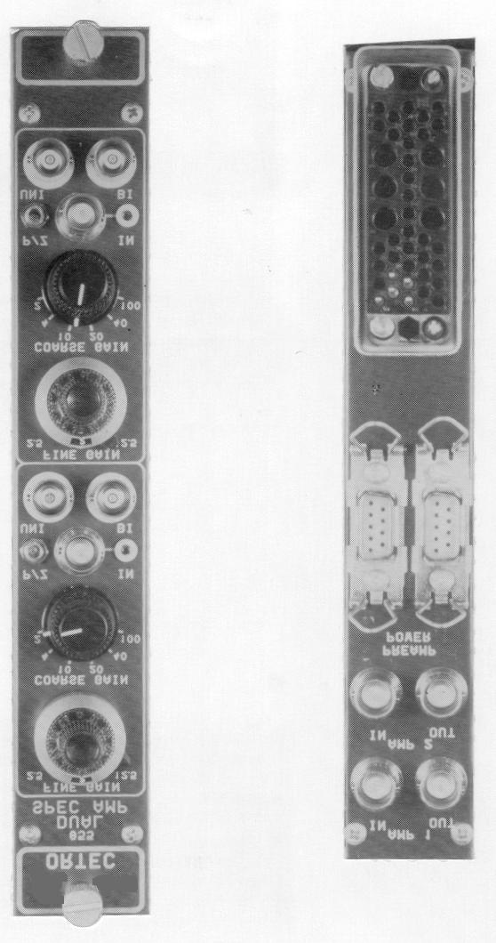
7 1 ORTEC MODEL 855 DUAL SPECTROSCOPY AMPLIFIER 1. DESCRIPTION 1.1. GENERAL The ORTEC 855 Amplifier is two spectroscopy amplifiers in a single-width NIM module that feature a versatile combination of jumper-selectable pulse shaping characteristics. The amplifier has extremely low noise, a wide gain range, and excellent overload response for universal application in high-resolution spectroscopy. It accepts input pulses of either polarity. Input may originate from germanium or silicon semiconductor detectors, from scintillation counters with either fast or slow scintillators, from proportional counters, from pulsed ionization chambers, from electron multipliers, etc. The unit has an input impedance of 1000 and accepts either positive or negative input pulses with rise times <650 ns and fall times >30 µs. Three integration and differentiation time constants are jumper-selectable on the printed wiring board (PWB) to provide optimum shaping for resolution and count rate. The differentiation network has variable pole-zero cancellation that can be adjusted to match preamplifiers with decay times >30 µs. The pole-zero cancellation drastically reduces the undershoot after the differentiator and greatly improves overload and count rate characteristics. In addition, the amplifier contains an active, filtershaping network that optimizes the signal-to-noise ratio and minimizes the overall resolving time. The amplifier has unipolar and bipolar BNC outputs. The unipolar output is used for spectroscopy in systems where do coupling can be maintained from the 855 to the analyzer. A BLR (baseline restorer) circuit is included in the unit for improved performance at all count rates. Baseline correction is applied only during intervals between input pulses and automatically selects a discriminator level to identify input pulses. The unipolar output do level is within the range of 5 mv to +5 mv. This output permits the use of the direct-coupled input of the analyzer with a minimum amount of interface problems. The 855 can be used for constant-fraction timing when operated in conjunction with an ORTEC 551,552, or 553 Timing Single-Channel Analyzer. The ORTEC Timing Single-Channel Analyzers feature a minimum of walk as a function of pulse amplitude and incorporate a variable delay time on the output pulse to enable the timing pickoff output to be placed in time coincidence with other signals. The 855 has complete provisions, including power distribution, for operating any ORTEC solid-state preamplifier. Normally. the preamplifier pulses should have a rise time of 0.25 µs or less to properly match the amplifier filter network and a decay time >30 µs for proper pole-zero cancellation. The input impedance is When long preamplifier cables are used, the cables can be terminated in series at the preamplifier end or in shunt at the amplifier end with the proper resistors. The output impedance is -0.2 and the output can be connected to other equipment by a single cable going to all equipment. The cable must be shunt-terminated at the far end. (See Section 3 for further information.) 1.2. POLE-ZERO CANCELLATION Pole-zero cancellation is a method for eliminating pulse undershoot after the differentiating network. In an amplifier not using pole-zero cancellation (Fig. 1.1.) the exponential tail on the preamplifier output signal (usually 50 to 500 µs) causes an undershoot whose peak amplitude is roughly determined from: undershoot amplitude differentiated pulse amplitude = differentiation time preamplifier pulse decay time. For a I-µs differentiation time and a 50-µs pulse decay time the maximum undershoot is 2%, and this decays with a 50-µs time constant. Under overload conditions, this undershoot is often sufficiently large to saturate the amplifier during a
8 2 considerable portion of the undershoot, causing excessive dead time. This effect can be reduced by increasing the preamplifier pulse decay time (which generally reduces the counting rate capabilities of the preamplifier) or compensating for the undershoot by providing pole-zero cancellation. Pole-zero cancellation is accomplished by the network shown in Fig The pole (s + (1/T o )) due to the preamplifier pulse decay time is canceled by the zero of the network [s + (k/r 2 C 1 )l. In effect, the dc path across the differentiation capacitor adds an attenuated replica of the preamplifier pulse to just cancel the negative undershoot of the differentiating network. Total preamplifier-amplifier pole-zero cancellation requires that the preamplifier output pulse decay time be a single exponential decay and be matched to the pole-zero cancellation network. The variable pole-zero cancellation network allows accurate cancellation for all preamplifiers having 30-µs or greater decay times. Improper matching of the pole-zero network will degrade the overload performance and cause excessive pileup distortion at medium counting rates. Improper matching causes either an under-compensation (undershoot is not eliminated) or an overcompensation (output after the main pulse does not return to the baseline but decays to the baseline with the preamplifier time constant). The pole-zero adjust is accessible on the front panel of the 855 and can easily be adjusted by observing the baseline on an oscilloscope with a monoenergetic source or pulser having the same decay time as the preamplifier under overload conditions. The adjustment should be made so that the pulse returns to the baseline in the minimum time with no undershoot ACTIVE FILTER When only FET gate current and drain thermal noise are considered, the best signal-to-noise ratio occurs when the two noise contributions are equal for a given input pulse shape. The gaussian pulse shape (Fig. 1.3.) for this condition requires an amplifier with a single RC differentiation and n equal RC integrations where n approaches infinity. The Laplace transform of this transfer function is G(s) s s(1/rc) X 1 [s(1/rc)] n (n ) where the first factor is the single differentiation, and the second factor is the n integrations. The active filter approximates this transfer function.
9 3 Figure 1.3. illustrates the results of pulse shaping in an amplifier. Of the four pulse shapes shown the cusp would produce minimum noise, but this is impractical to achieve with normal electronic circuitry and would be difficult to measure with an ADC. The true gaussian shape deteriorates the signal-to-noise ratio by only about 12% from that of the cusp and produces a signal that is easy to measure but requires many sections of integration (n Ú ). With two sections of integration the waveform identified as a gaussian approximation can be obtained, and this deteriorates the signal-tonoise ratio by about 22%. The ORTEC active filter network in the 855 provides a fourth waveform in Fig. 1.3.; this waveform has characteristics superior to the n = 2 gaussian approximation, yet obtains them with two complex poles and a real pole. By this method, the output pulse shape has a good signal-to-noise ratio, is easy to calculate, and yet requires only a practical amount of electronic circuitry to achieve the desired results.
10 4 2. SPECIFICATIONS The ORTEC 855 Amplifier is two spectroscopy amplifiers in a single-width NIM module. Only one amplifier will be referred to in the discussion. All references, such as jumper settings, input/output connections, specifications, etc., apply to both amplifiers PERFORMANCE GAIN RANGE Continuously adjustable from 5 to PULSE SHAPE Semigaussian on all ranges with peaking time equal to 2.22, 50% pulse width equal to 3.32, and pulse width at 0.1% level equal to 4.0 times the peaking time. Bipolar crossover = INTEGRAL NONLINEARITY <±0.05% for 1.5-µs shaping time. NOISE <5 µv rms referred to the input using 3 µs unipolar shaping; <7 µv using 1.5.µs shaping; both for again 100. TEMPERATURE INSTABILITY Gain ±0.0075%/(C, 0 to 50(C. DcLevel ±30 µv/(c, 0 to 50(C. WALK ±5 ns at 0.5 µs shaping for 50:1 dynamic range including contribution of an ORTEC 551 or 552 Constant-Fraction Timing Single-Channel Analyzer. OVERLOAD RECOVERY Recovers to within 2% of rated output from X300 overload in 2.5 nonoverload pulse widths using maximum gain for unipolar output. Same recovery from X500 overload for bipolar. RESTORER Gated active baseline stabilizer with automatic threshold circuit to provide the threshold level as a function of signal noise to the baseline restorer discriminator. SPECTRUM BROADENING Typically <10% FWHM for a 60 Co 1.33-MeV gamma line at 85% of full scale for an incoming count rate of 1 to 50k cps. Unipolar output, 1.5 µs shaping. SPECTRUM SHIFT 1 Peak position shifts typically <0.02% for a 60 Co 1.33-MeV gamma line at 85% of full scale (measured at the unipolar output, 1.5 µs shaping, 1 to 50k cps) CONTROLS FINE GAIN Ten-turn precision potentiometer with graduated dial for continuously variable directreading gain factor of X2.5 to X12.5. COARSE GAIN Six-position switch selects feedback resistors for gain factors of 2, 4, 10, 20, 40, and 100. SHAPING TIME Three-position printed wiring board (PWB) jumpers, easily accessible through side panel, select time constants for active pulseshaping filter network of 0.5, 1.5, or 3 µs. POS/NEG A PWB jumper (W3) selects either positive or negative input polarity. PZADJ Screwdriver adjustable potentiometer to set the pole-zero cancellation to compensate input decay times from 30 µs to INPUT INPUT BNC (UG-1094A/U) front and rear panel connectors accept either positive or negative pulses with rise times of 10 to 650 ns and decay times of 30 µs to, Z in = 1000 dc-coupled, linear maximum 2 V; absolute maximum 20 V OUTPUTS UNI Front panel BNC connector with Z o < 1. Short-circuit proof; full-scale linear range of 0 to +10 V; active filter shaped; dc-restored with dc level adjustable to ±15 mv. BI Front panel BNC connector with Z o < 1. Shortcircuit proof; positive lobe leading and full-scale linear range of 0 to +10 V; active filter shaped. 1 These count rate specifications were measured with a 10% HPGe detector. Detectors with a large number of slow, risetime signals will most likely give poorer results.
11 5 Rear panel BNC connector with Z o = 93. PWB jumper (W8) selects either unipolar or bipolar rear panel output. PREAMP POWER Rear panel standard ORTEC power connector (Amphenol ) mates with captive and noncaptive power cords on all ORTEC preamplitiers RELATED EQUIPMENT The ORTEC 855 Amplifier accepts linear pulses from, and furnishes power to, any standard ORTEC preamplifier or equivalent. Its output pulses may be used for linear signal analysis, using any of the ORTEC modular instruments and multichannel analyzers ELECTRICAL AND MECHANICAL POWER REQUIRED +24V, 83mA; 24V, 7OmA; +12V, 125 ma; 12 V, 140 ma. WEIGHT Net 1.5 kg (3.3 lb). Shipping 3.1 kg (7.0 lb). DIMENSIONS Standard single-width NIM module 3.43 x cm (1.35 x in.) per TID (Rev). 3. INSTALLATION The ORTEC 855 Amplifier is two spectroscopy amplifiers in a single-width NIM module. Only one amplifier will be referred to in the discussion. All references, such as jumper settings, input/output connections, specifications, etc., apply to both amplifiers GENERAL The 855 operates on power that must be furnished from a NIM-standard bin and power supply such as the ORTEC 40OIA/4002A Series. The bin and power supply is designed for relay rack mounting. If the equipment is to be rack mounted, be sure that there is adequate ventilation to prevent any localized heating of the components used in the 855. The temperature of equipment mounted in racks can easily exceed the maximum limit of 50(C unless precautions are taken CONNECTION TO POWER The 855 contains no internal power supply and must obtain the necessary dc operating power from the bin and power supply in which it is installed for operation. Always turn off power for the power supply before inserting or removing any modules. After all modules have been in- stalled in the bin and any preamplifiers have also been connected to the Preamp Power connectors on the amplifiers, cheek the dc voltage levels from the power supply to see that they are not overloaded. The ORTEC 4001A/4002A Series Bins and Power Supplies have convenient test points on the power supply control panel to permit monitoring these dc levels. If any one or more of the dc levels indicates an overload, some of the modules will need to be moved to another bin to achieve operation CONNECTION TO PREAMPLIFIER The preamplifier output signal is connected to the 855 through the Input BNC connectors on the front and rear panels. The input impedance is 1000 and is dc-coupled to ground; therefore, the preamplifier output must be either ac-coupled or have approximately zero dc voltage under no-signal conditions. The 855 incorporates pole-zero cancellation to enhance the overload and count rate characteristics of the amplifier. This technique requires matching the network to the preamplifier decay-time constant to achieve perfect compensation. The pole-zero adjustment should be set each time the preamplifier or the shaping time constant of the amplifier is changed. For details of the pole-zero adjustment see Section 4.5. An alternate method is accomplished easily by using a monoenergetic source and observing the amplifier baseline with an oscilloscope after each pulse under X2 overload conditions. Adjustment should be made so that the pulse returns to the baseline in a minimum amount of time with no undershoot. Preamplifier power at +24 V, 24 V, +12 V, and 12 V is available through the Preamp Power connector on the rear panel. When the preamplifier is connected, its power requirements are obtained from the same bin and power supply as is used for the amplifier, and this increases the dc loading on
12 6 each voltage level over and above the requirements for the unit at the module position in the bin. When the 855 is used with a remotely located preamplifier (i.e., preamplifier-to-amplifier connection through 25 ft or more of coaxial cable), be careful to ensure that the characteristic impedance of the transmission line from the preamplifier output to the 855 input is matched. Because the input impedance of the 855 is 1000, sending-end termination will normally be preferred; the transmission line should be seriesterminated at the preamplifier output. All ORTEC preamplifiers contain series terminations that are either 93 or variable; coaxial cable type RG-62/U or RG-71/U is recommended CONNECTION OF TEST PULSE GENERATOR THROUGH A PREAMPLIFIER The satisfactory connection of a test pulse generator (such as the ORTEC 419 Precision Pulse Generator or equivalent) depends primarily on two considerations: the preamplifier must be properly connected to the unit as discussed in Section 3.3, and the proper input signal simulation must be applied to the preamplifier. To ensure proper input signal simulation, refer to the instruction manual for the particular preamplifier being used. DIRECTLY INTO THE 855 Since the input of the 855 has input impedance, the test pulse generator will normally have to be terminated at the amplifier input with an additional shunt resistor. In addition, if the test pulse generator has a dc offset, a large series isolating capacitor is also required because the 855 input is dc coupled. The ORTEC test pulse generators are designed for direct connection. When any one of these units is used, it should be terminated with a 100- terminator at the amplifier input or be used with at least one of the output attenuators set at In. (The small error due to the finite input impedance of the amplifier can normally be neglected.) SPECIAL CONSIDERATIONS FOR POLE-ZERO CANCELLATION When a tail pulser is connected directly to the amplifier input, the PZ ADJ should be adjusted if overload tests are to be made (other tests are not affected). See Section 4.5 for the polezero adjustment. It a preamplifier is used and a tail pulser is connected to the preamplifier test input, similar precautions are necessary. In this case the effect of the pulser decay must be removed; that is, a step input should be simulated SHAPING CONSIDERATIONS The shaping time constant on the 855 is selectable by PWB-mounted jumpers in steps of 0.5, 1.5. and 3 µs. The choice of the proper shaping time constant is generally a compromise between operating at a shorter time constant for accommodation of high counting rates and operating with a longer time constant for a better signal-to-noise ratio. For scintillation counters, the energy resolution depends largely on the scintillator and photomultiplier, and therefore a shaping time constant of about four times the decay-time constant of the scintillator is a reasonable choice (for Nal, a 1.5-µs shaping time constant is about optimum). For gas proportional counters, the collection time is normally in the 0.5 to 5 µs range and a 1.5 µs or greater time constant selection will generally give optimum resolution. For surface barrier semiconductor detectors, a 0.5- to 2-µs resolving time will generally provide optimum resolution. Shaping time for Ge(Li) detectors will vary from 1.5 to 6 µs, depending on the size, configuration, and collection time of the specific detector and preamplifier. When a charge-sensitive preamplifier is used, the optimum shaping time constant to minimize the noise of a system can be determined by measuring the output noise of the system and dividing it by the system gain. The 855 has almost constant gain for all shaping modes; therefore, the optimum shaping can be determined by measuring the output noise with a voltmeter as each shaping time constant is selected LINEAR OUTPUT CONNECTIONS AND TERMINATING CONSIDERATIONS Since the 855 unipolar output is normally used for spectroscopy, the unit is designed with the flexibility to interface the pulse with an analyzer. A gated baseline restorer (BLR) circuit is included in this output for improved performance at all count rates. The threshold for the restorer gate is determined automatically, according to the input noise level. The unipolar output dc level is 0 ± 5 mv. Three general methods of termination are used. The simplest of these is shunt termination at the receiving end of the cable. A second method is series termination at the sending end. The third is a combination of series and shunt termination, where the cable impedance is matched both in
13 7 series at the sending end and in shunt at the receiving end. The combination is most effective, but this reduces the amount of signal strength at the receiving end to 50% of that which is available in the sending instrument. To use shunt termination at the receiving end of the cable, connect the output from the 855 front or rear panels through 93- cable to the input of the receiving instrument. Then use a BNC tee connector to attach both the interconnecting cable and a 100- terminator at the input connector of the receiving instrument. Since the input impedance of the receiving instrument is normally 1000 or more. the effective instrument input impedance with the 100- terminator will be of the order of 93, and this will match the cable impedance correctly SHORTING OR OVERLOADING THE AMPLIFIER OUTPUT The 855 output is dc-coupled with an output impedance of 0.2. If the output is shorted with a direct short circuit, the output stage will limit the peak current of the output so that the amplifier will not be harmed. When the amplifier is terminated with 100, the maximum count rate consistent with linear output is RATE max cps 2 x 10 V o where V o is the peak output pulse amplitude in volts (V) and 2 is the shaping time in µs. For customer convenience, ORTEC stocks the proper terminators and BNC tees, or they can be ordered from a variety of commercial sources. 4. OPERATION 4.1. INITIAL TESTING AND OBSERVATION OF PULSE WAVEFORMS Refer to Section 6 for information on testing performance and observing waveforms at front panel test points. Figure 4.1. shows typical output waveforms FRONT PANEL CONTROLS GAIN A Coarse Gain switch and a Gain control (a precision 10-turn locking potentiometer) select and precisely adjust the gain factor for the amplification in the 855. Switch settings are X2, 4, 10, 20, 40, and 100. Continuous fine gain range is from XO.5 to X12.5 using markings of 500 through 1250 dial divisions. Using these controls collectively, the gain can be set at any level from X5 through X1250. POS/NEG A PWB jumper (W3) selects an input circuit that accepts either polarity of pulses from the preamplifier. PZ ADJ A screwdriver control sets the pole-zero cancellation to match the preamplifier pulse decay characteristics. The range is from 30 µs to. SHAPING PWB jumpers select equal integration and differentiation time constants to shape the input pulses. Settings are 0.5, 1.5, and 3 µs. Illustrated drawings and instructions for setting time-constant jumpers are shown in Fig. 4.2.

14 8 Fig Set Jumpers W1, W2, W4 W7, and W9 as Shown, in Both Channel 1 and Channel 2, to Select Desired Time Constant (figure shows setting of 1.5 µs) PANEL CONNECTIONS INPUTS Accept input pulses to be shaped and/or amplified by the 855. Compatible characteristics; positive or negative with rise time from 10 to 650 ns; decay time >30 µs for proper pole-zero cancellations; input linear amplitude range 0 to 2 V with a maximum limit of ±20 V. Input impedance is OUTPUTS UNI Front panel BNC connector with Z o < 1. Short-circuit proof; full-scale linear range of 0 to +10 V; active filter shaped; dc-restored with dc level adjustable to ±15 mv. BI Front panel BNC connector with Z o < 1. Shirtcircuit proof; positive lobe leading and full-scale linear range of 0 to +10 V; active filter shaped. Rear panel BNC connector with Z o = 93. PWB jumper (W8) selects either bipolar or unipolar rear panel output. PREAMP POWER Rear panel standard ORTEC power connector (Amphenol ) mates with captive and noncaptive power cords on all ORTEC preamplifiers STANDARD SETUP PROCEDURE a. Connect the detector, preamplifier, highvoltage power supply, and preamplifier into a basic system and connect the amplifier output to an oscilloscope. Connect the preamplifier power cable to the Preamp connector on the
15 9 855 rear panel. Turn on power in the bin and power supply and allow the electronics of the system to warm up and stabilize. b. Set the 855 controls initially as follows: Shaping 1.5,µs Coarse Gain 10 Fine Gain 5.00 Pos/Neg Match input pulse polarity c. Use a 6O Co calibration source; place it about 25 cm from the active face of the detector. The unipolar output pulse from the 855 should be about 8 to 10 V using a preamplifier with a conversion gain (charge sensitivity) of' 170 mv/mev. d. Readjust the Gain control so that the higher peak from the 60 Co source (1.33 MeV) provides an amplifier output at 9 V POLE-ZERO ADJUSTMENT The pole-zero adjustment is extremely critical for good performance at high count rates. This adjustment should be checked carefully for the best possible results. USING A GERMANIUM SYSTEM AND 6O Co a. Adjust the radiation source count rate between 2 khz and 10 khz. b. Observe the unipolar output with an oscilloscope. Adjust the PZ ADJ control so that the pulse trailing edges return to the baseline without overshoot or undershoot (Fig. 4.3). The oscilloscope used must be dc coupled and must not contribute distortion in the observed waveforms. Oscilloscopes such as Tektronix 453, 454,465, and 475 will overload for a 10-V signal when the vertical sensitivity is <100 mv/cm. To prevent overloading the oscilloscope, use the clamp circuit shown in Fig Fig Typical Waveform Illustrating Pole-Zero Adjustment Effects; Oscilloscope Trigger, Internal Pos., 60Co Source with 1.33-MeV Peak Adjusted 9 V; Count Rate 3 khz; Shaping Time Constant 1.5 µs.

16 10 Fig A Clamp Circuit That Can Be Used to Prevent Overloading the Oscilloscope Input. USING SQUARE WAVE THROUGH PREAMPLIFIER TEST INPUT A more precise pole-zero adjustment in the 855 can be obtained by using a square wave signal as the input to the preamplifier. Many oscilloscopes include a calibration output on the front panel, and this is a good source of square wave signals at a frequency of 1 khz. The amplifier differentiates the signal from the preamplifier so that it generates output signals of alternate polarities on the leading and trailing edges of the square wave input signal, and these can be compared as shown in Fig. 4.5 to achieve excellent pole-zero cancellation. Use the following procedure: a. Remove all radioactive sources from the vicinity of the detector. Set up the system as for normal operation, including detector bias. b. Set tire 855 controls as for normal operation; this includes gain, shaping, and input polarity. c. Connect the source of 1-kHz square waves through an attenuator to the Test input of the preamplifier. Adjust the attenuator so that the 855 output amplitude is -9 V. d. Observe the Unipolar output of the 855 with an oscilloscope. Adjust the PZ ADJ control for proper response according to Fig Use the clamp circuit in Fig. 4.4 to prevent overloading the oscilloscope input.
17 OPERATION WITH SEMICONDUCTOR DETECTORS CALIBRATION OF TEST PULSER An ORTEC 419 Precision Pulse Generator (or equivalent) is easily calibrated so that the maximum pulse height dial reading (1000 divisions) is equivalent to 10-MeV loss in a silicon radiation detector. The procedure is as follows: a. Connect the detector to be used to the spectrometer system; that is, preamplifier, main amplifier, and biased amplifier. b. Allow excitation from a source of known energy (e.g., alpha particles) to fall on the detector. c. Adjust the amplifier gain and the bias level of the biased amplifier to give a suitable output pulse. d. Set the pulser Pulse Height control at the energy of the alpha particles striking the detector (e.g., set the dial at 547 divisions for a 5.47-MeV alpha particle energy). e. Turn on the pulser and use its Normalize control and attenuators to set the output due to the pulser for the same pulse height as the pulse obtained in step c. Lock the Normalize control and do not move it again until recalibration is required. The pulser is now calibrated; the Pulse Height dial reads directly in MeV if the number of dial divisions is divided by 100. AMPLIFIER NOISE AND RESOLUTION MEASUREMENTS As shown in Fig. 4.6, a preamplifier, amplifier, pulse generator, oscilloscope, and wide-band rms voltmeter such as the Hewlett-Packard 3400A are required for this measurement. Connect a suitable capacitor to the input to simulate the detector capacitance desired. To obtain the resolution spread due to amplifier noise: a. Measure the rms noise voltage (E rms ) at the amplifier output. b. Turn on the 4l9 precision pulse generator and adjust the pulser output to any convenient readable voltage, E o, as determined by the oscilloscope. The full-width-half-maximum (FWHM) resolution spread due to amplifier noise is then N(FWHM ) 2.35 E rms E dial E O where E dial is the pulser dial reading in MeV, and 2.35 is the factor for rms to FWHM. For averageresponding voltmeters such as the Hewlett-Packard 400D, the measured noise must be multiplied by 1.13 to calculate the rms noise. The resolution spread will depend on the total input capacitance, because the capacitance degrades the signal-to-noise ratio much faster than the noise. DETECTOR NOISE-RESOLUTION MEASUREMENTS The measurement just described can be made with a biased detector instead of the external capacitor that would be used to simulate detector capacitance. The resolution spread will be larger because the detector contributes both noise and capacitance to the input. The detector noiseresolution spread can be isolated from the amplifier noise spread if the detector capacitance is known, since (N Det ) 2 (N Elec ) 2 (N Total ) 2
18 12 where N total is the total resolution spread, and N elec is the electronic resolution spread when the detector is replaced by its equivalent capacitance. The detector noise tends to increase with bias voltage, while the detector capacitance decreases. The net change in resolution spread will depend upon which effect is dominant. Figure 4.7 shows curves of typical noise-resolution spread versus bias voltage using data from several ORTEC silicon surface-barrier semi-conductor radiation detectors. The electronic noise-resolution spread can be measured directly with a pulse height analyzer and the mercury pulser as follows: a. Select the energy of interest with an ORTEC 419 Precision Pulse Generator. Set the amplifier and biased amplifier gain and bias level controls so that the energy is in a convenient channel of the analyzer. b. Calibrate the analyzer in kev per channel, using the pulser; full scale on the pulser dial is 10 MeV when calibrated as described above. c. Obtain the amplifier noise-resolution spread by measuring the FWHM of the pulser peak in the spectrum. The detector noise-resolution spread for a given detector bias can be determined in the same manner by connecting a detector to the preamplifier input. The amplifier noise resolution spread must be subtracted as described in Detector Noise- Resolution Measurements. The detector noise will vary with detector size and bias conditions and possibly with ambient conditions. AMPLIFIER NOISE-RESOLUTION MEASUREMENTS USING MCA Probably the most convenient method of making resolution measurements is with a pulse height analyzer, as shown by the setup illustrated in Fig CURRENT VOLTAGE MEASUREMENTS FOR Si AND Ge DETECTORS The amplifier system is not directly involved in semiconductor detector current voltage measurements, but the amplifier serves to permit noise monitoring during the setup. The detector noise measurement is a more sensitive method than a current measurement of determining the maximum detector voltage that should be used because the noise increases more rapidly than the reverse current at the onset of detector breakdown. Make this measurement in the absence of a source. Figure 4.9 shows the setup required for current voltage measurements. An ORTEC 428 Bias Supply is used as the voltage source. Bias voltage should be applied slowly and reduced when noise increases rapidly as a function of applied bias. Figure 4.10 shows several typical current voltage curves for ORTEC silicon surface-barrier detectors. When it is possible to float the microammeter at the detector bias voltage, the method of detector current measurement shown by the dashed lines in Fig. 4.9 is preferable. The detector is grounded as
19 13 in normal operation, and the microammeter is connected to the current monitoring jack on the 428 detector supply. Accumulate the alpha peak in the MCA. b. Slowly increase the bias level and biased amplifier gain until the alpha peak is spread over 5 to 10 channels and the minimum- to maximum-energy range desired corresponds to the first and last channels of the MCA. c. Calibrate the analyzer in kev per channel using the purser and the known energy of the alpha peak (see "Calibration of Test Pulser") or two known-energy alpha peaks. d. Calculate the resolution by measuring the number of channels at the FWHM level in the peak and converting this to kev. HIGH-RESOLUTION GAMMA SPECTROSCOPY SYSTEM A high-resolution gamma spectroscopy system block diagram is shown in Fig Although a biased amplifier is not shown (an analyzer with more channels being preferred), it can be used if the only analyzer available has fewer channels and only higher energies are of interest. When a germanium detector that is cooled by a liquid nitrogen cryostat is used, it is possible to obtain resolutions from about 1 kev FWHM up (depending on the energy of the incident radiation and the size and quality of the detector). Reasonable care is required to obtain such results. Some guidelines for obtaining optimum resolution are: 4.7. OPERATION IN SPECTROSCOPY SYSTEMS HIGH-RESOLUTION ALPHA-PARTICLE SPECTROSCOPY SYSTEM The block diagram of a hig-resolution spectroscopy system for measuring natural alpha particle radiation is shown in Fig Since natural alpha radiation occurs only above several MeV, an ORTEC 444 Biased Amplifier is used to suppress the unused portion of the spectrum; the same result can be obtained by using digital suppression on the MCA in many cases. Alpha-particle resolution is obtained in the following manner: a. Keep interconnection capacitance between the detector and preamplifier to an absolute minimum (no long cables). b. Keep humidity low near the detectorpreamplifier junction. c. Operate the amplifier with the shaping time that provides the best signal-to-noise ratio. d. Operate at the highest allowable detector bias to keep the input capacitance low. a. Use appropriate amplifier gain and minimum biased amplifier gain and bias level.
20 14 SCINTILLATION-COUNTER GAMMA SPECTROSCOPY SYSTEMS The ORTEC 855 can be used in scintillationcounter spectroscopy systems as shown in Fig The amplifier shaping time constants should be selected in the region of 0.5 to 1.5 µs for Nal or plastic scintillators. For scintillators having longer decay times, longer time constants should be selected. X-RAY SPECTROSCOPY USING PROPORTIONAL COUNTERS Space charge effects in proportional counters, operated at high gas amplification, tend to degrade the resolution capabilities drastically at x-ray energies, even at relatively low counting rates. By using a high-gain, low-noise amplifying system and lower gas amplification, these effects can be reduced and a considerable improvement in resolution can be obtained. The block diagram in Fig shows a system of this type. Analysis can be accomplished by simultaneous acquisition of all data on a multichannel analyzer or counting a region of. interest in a single-channel analyzer window with a counter and timer or counting ratemeter OTHER EXPERIMENTS Block diagrams illustrating how 855 and other ORTEC modules can be used for experimental setups for various other applications are shown in Figs. 4.15, 4.16, and 4.17.
21 15
22 16
23 17 5. CIRCUIT DESCRIPTION Figure 5.1 is a block diagram of the instrument. Much of the circuitry has been designed to use integrated circuits. This advanced technology achieves an economical high-density package with high reliability. The signal passes through a differentiator, with a time constant that is selected by W5, to the inverting differential amplifier formed by transistors Q1 through Q6. The nominal gain of this stage is 4.5 Dc-coupling for the input is furnished through the pole-zero cancellation circuit; the current for this.circuit is a function of the setting of the PZ ADJ control (R1) and the resistance path selected by W5 and by the pulse that is being compensated. Integrated circuits U4 and U2 are the gain stages. Feedback around each stage controls the gain. The gain of U4 is X1 or X1O as selected by Coarse Gain switch S2A. For U2, the fine gain is controlled by R30. Switch S2B allows selection of input resistors to vary the coarse gain. The output of U2 is processed through an active integrator amplifier, U1, that provides a complex pole pair. The real pole of the differentiator at the input is 1.05 times the value of the real part of complex pole pair. The shaping time constant is selected by jumper W1, determining which, resistances are used to control the time constant. Amplifier U1 is connected in a noninverting configuration with a dc gain of 1.42 as set by R3 and R4. The output of U1 is inverted by the input polarity amplifier U3. The input polarity jumper, W3, selects either the output of U3 for a positive input or the noninverted output of U1 for a negative input pulse. The output of W3 is furnished to the bipolar output stage, A3, through a differentiator. The time constant selected by W7 and W9 determines the capacitance in this ac-coupling, and the output of A3 is the signal that is provided through the B1 (Bipolar) connectors on the front and rear panels. Resistor R103 is the series 93- termination for the rear panel connection. The output of W3 is also furnished to the unipolar output stage, A2. The signal is furnished to the input of A2 through R76 and R78. The hybrid circuit, A2, drives the output signal through the UNI (Unipolar) connectors on the front and rear panels. Resistor R102 is the series 93 termination for the rear panel connection. Transistors Q10, Q11, Q12, and Q13 limit the average dc current through the output amplifiers to 35 ma. The BLR (baseline restorer) circuit stabilizes the unipolar output stage within a few mv of zero determined by dc stability of U7. The BLR circuit consists of amplifier U7 and gated transconductance amplifier U6 with C30 and Q7. The correction is accumulated as a charge on C30 and applied through FET Q7 to A2. U6 is gated on during intervals when no input signal is present, and is gated off when a signal is present to prevent interference with the pulses of interest and to prevent the pulse amplitudes from affecting the average charge on C30. Gating is provided by the baseline discriminator U5. The gate permits correction between input signals by identifying when signals are present and preventing the correction during these intervals. The negative restorer gate threshold is set at 400 mv for use with resetting-type preamplifiers. The unipolar output is amplified at U7 providing the input for U5, U6, and the Auto Noise Level (ANL) circuitry. When the signal is greater than the dc threshold set by the ANL, U5 turns on, driving Q8 to turn off current source Q9 that supplies the restorer current for U6. Hybrid A1 establishes an automatic BLR threshold level that is related to the output noise level.
24 18 6. MAINTENANCE 6.1. TEST EQUIPMENT REQUIRED The following test equipment should be used to adequately test the specifications of the 855 amplifier: 1. ORTEC 419 Precision Pulse Generator or 448 Research Pulser. 2. Tektronix 547 Series Oscilloscope with a type 1A1 plug-in or equivalent. 3. Hewlett-Packard 3400A rms voltmeter PULSER TEST 2 FUNCTIONAL CHECKS Set the 855 controls as follows: Coarse Gain 100 Gain 7.5 Input Polarity Neg Shaping Time Constant 1.5 µs a. Connect a positive pulser output to the 855 input and adjust the pulser to obtain +10 V at the unipolar output. This should require an input pulse of 13.3 rnv using a 100- terminator at the input. Adjust PZ if necessary. 2 See IEEE Standards No b. Change the input polarity jumper (W3) to Pos and then back to Neg while monitoring the output for a polarity inversion. c. Monitor the bipolar output for dc level of <± mv; pulse shape should be bipolar. Return to UNI. d. Recheck the output pulse amplitude and adjust if necessary to set it at +10 V with maximum gain. Decrease the Coarse Gain switch stepwise from 100 to 2 and ensure that the output amplitude changes by the appropriate amount for each step. Return the Coarse Gain switch to 100. e. Decrease the Gain control from 7.5 to 2.5 and check to see that the output amplitude decreases by a factor of 2. Return the Gain control to maximum at 7.5. f. With the shaping jumpers set for 1.5 µs, measure the time to the peak on the unipolar output pulse; this should be 3.3µs (or 2.22). Measure the time to baseline crossover of the bipolar output; this should be 5.0 µs (or 3.32). g. Change the shaping jumpers to O.5 and 3 µs in turn. At each setting, check to see that the time to the unipolar peak is Return the jumpers to 1.5 µs.
25 19 OVERLOAD TESTS Start with maximum gain, 2 = 1.5 µs, and a +10V output amplitude. Increase the pulser output amplitude by X200 and observe that the unipolar output returns to within 200 mv of the baseline within 24 µs after the application of a single pulse from the pulser. It will probably be necessary to vary the PZ ADJ control on the front panel in order to cancel the pulser pole and minimize the time required for return to the baseline. LINEARITY The integral nonlinearity of the 855 can be measured by the technique shown in Fig In effect, the negative pulser output is subtracted from the positive amplifier output to cause a null point that can be measured with excellent sensitivity. The pulser output must be varied between 0 to 10 V, which usually requires an external control source for the pulser. The amplifier gain and the pulser attenuator must be adjusted to measure 0 V at the null point when the pulser output is 10 V. The variation in the null point as the pulser is reduced gradually from 10 V to 0 V is a measure of the nonlinearity. Since the subtraction network also acts as a voltage divider, this variation must be less than (10 V full scale) x (±0.05% maximum nonlinearity) x (1/2 for divider network) = ±2.5 mv for the maximum null-point variation. OUTPUT LOADING Use the test setup of Fig Adjust the amplifier output to 10 V and observe the null point when the front panel output is terminated in 100. The change should be <2.5 mv. NOISE Measure the noise at the amplifier unipolar output with maximum amplifier gain and 3-µs shaping time. Using a true-rms voltmeter, the noise should be <5 µv x 750 (gain), or 3.75 mv. For an average responding voltmeter, the noise reading would have to be multiplied by 1.13 to calculate the rms noise. The input must be terminated in 100 during the noise measurements SUGGESTIONS FOR TROUBLESHOOTING In situations where the 855 is suspected of a malfunction, it is essential to verify such malfunction in terms of simple pulse generator impulses at the input. The unit must be disconnected from its position in any system and routine diagnostic analysis performed with a test pulse generator and an oscilloscope. It is imperative that testing not be performed with a source and detector until the amplifier performs satisfactorily with the test pulse generator. The testing instructions in Section 6.2 and the circuit descriptions in Section 5 should provide assistance in locating the region of trouble and repairing the malfunction. The two side plates can be completely removed f rom the module to enable oscilloscope and, voltmeter observations FACTORY REPAIR This instrument can be returned to the ORTEC factory for service and repair at a nominal cost. Our standard procedure for repair ensures the same quality control and checkout as for a new instrument. Always contact Customer Services at
26 20 ORTEC, (865) , before sending in an instrument for repair to obtain shipping instructions. A Return Authorization Number is required and will be assigned to the unit. This number should be marked on the address label and on the package to ensure prompt attention when the unit reaches the factory TABULATED TEST POINT VOLTAGES The voltages given in Table 6.1 are intended to indicate typical dc levels that can be measured on the PWB. In some cases the circuit will perform satisfactorily even though, due to component tolerances, there may be some voltage measurements which differ slightly from the listed values. The tabulated values should not be interpreted as absolute voltages but rather should be used as an aid during troubleshooting. Table 6.1. Typical dc Voltages Note: All voltages measured with no input signal, with the input terminated in 100, and all controls set fully clockwise at maximum. Location Tl T2 T3 T4 T5 T6 T7 Voltage +-50 mv +60 mv ±0.7 V ±1.0 v ±60 rnv 0 to -0.8 V +6 mv Bin/Module Connector Pin Assignments for Standard Nuclear Instrument Modules per DOE/ER-0457T Pin Function Pin Function 1 +3 V 23 Reserved 2 3 V 24 Reserved 3 Spare Bus 25 Reserved 4 Reserved Bus 26 Spare 5 Coaxial 27 Spare 6 Coaxial * V 7 Coaxial *29 24 V V dc 30 Spare Bus 9 Spare 31 Spare *10 +6 V 32 Spare *11 6 V * V ac (Hot) 12 Reserved Bus *34 Power Return Ground 13 Spare 35 Reset (Scaler) 14 Spare 36 Gate 15 Reserved 37 Reset (Auxiliary) * V 38 Coaxial *17 12 V 39 Coaxial 18 Spare Bus 40 Coaxial 19 Reserved Bus * V ac (Neutral) 20 Spare *42 High-Quality Ground 21 Spare G Ground Guide Pin 22 Reserved Pins marked (*) are installed and wired in ORTEC s Model 4001A and 4001C Modular System Bins.
Model 863 Quad Timing Filter Amplifier Operating and Service Manual
 Model 863 Quad Timing Filter Amplifier Operating and Service Manual Printed in U.S.A. ORTEC Part No. 733960 0411 Manual Revision C Advanced Measurement Technology, Inc. a/k/a/ ORTEC, a subsidiary of AMETEK,
Model 9302 Amplifier-Discriminator Operating and Service Manual
 Model 9302 Amplifier-Discriminator Operating and Service Manual Printed in U.S.A. ORTEC Part No. 733690 1202 Manual Revision C Advanced Measurement Technology, Inc. a/k/a/ ORTEC, a subsidiary of AMETEK,
Model 533 Dual Sum and Invert Amplifier Operating and Service Manual
 Model 533 Dual Sum and Invert Amplifier Operating and Service Manual Printed in U.S.A. ORTEC Part No. 733410 1202 Manual Revision B Advanced Measurement Technology, Inc. a/k/a/ ORTEC, a subsidiary of AMETEK,
Model 113 Scintillation Preamplifier Operating and Service Manual
 Model 113 Scintillation Preamplifier Operating and Service Manual Printed in U.S.A. ORTEC Part No. 717560 1202 Manual Revision B Advanced Measurement Technology, Inc. a/k/a/ ORTEC, a subsidiary of AMETEK,
Model 9305 Fast Preamplifier Operating and Service Manual
 Model 9305 Fast Preamplifier Operating and Service Manual This manual applies to instruments marked Rev 03" on rear panel. Printed in U.S.A. ORTEC Part No.605540 1202 Manual Revision B Advanced Measurement
Model 427A Delay Amplifier Operating and Service Manual
 Model 427A Delay Amplifier Operating and Service Manual This manual Applies to instruments marked Rev 22" on rear panel Printed in U.S.A. ORTEC Part No. 733210 1202 Manual Revision B Advanced Measurement
Model 416A Gate and Delay Generator Operating and Service Manual
 Model 416A Gate and Delay Generator Operating and Service Manual Printed in U.S.A. ORTEC Part No. 733160 1202 Manual Revision E Advanced Measurement Technology, Inc. a/k/a/ ORTEC, a subsidiary of AMETEK,
ScintiPack Model 296 Photomultiplier Base with Preamplifier and High Voltage Power Supply Operating and Service Manual
 ScintiPack Model 296 Photomultiplier Base with Preamplifier and High Voltage Power Supply Operating and Service Manual WARNING This equipment generates, uses, and can radiate radio frequency energy, and
Model 428 Detector Bias Supply Operating and Service Manual
 Model 428 Detector Bias Supply Operating and Service Manual Printed in U.S.A. ORTEC Part No. 733220 1202 Manual Revision C Advanced Measurement Technology, Inc. a/k/a/ ORTEC, a subsidiary of AMETEK, Inc.
Model 480 Pulser Operating and Service Manual
 Model 480 Pulser Operating and Service Manual Printed in U.S.A. ORTEC Part No. 733390 1202 Manual Revision B Advanced Measurement Technology, Inc. a/k/a/ ORTEC, a subsidiary of AMETEK, Inc. WARRANTY ORTEC*
Model 673 Spectroscopy Amplifier and Gated Integrator Operating and Service Manual
 Model 673 Spectroscopy Amplifier and Gated Integrator Operating and Service Manual Printed in U.S.A. ORTEC Part No. 675590 0202 Manual Revision B $GYDQFHG 0HDVXUHPHQW 7HFKQRORJ\,QF a/k/a/ ORTEC, a subsidiary
Model 426 Linear Gate Operating and Service Manual
 Model 426 Linear Gate Operating and Service Manual This manual applies to instruments marked Rev 23" on rear panel Printed in U.S.A. ORTEC Part No. 733200 1202 Manual Revision B Advanced Measurement Technology,
Model 542 Linear Gate and Stretcher Operating and Service Manual
 Model 542 Linear Gate and Stretcher Operating and Service Manual NOTE: A substitution for the dual diode package (MSD6100) may have been made in this unit. If so, two 1N4153 diodes were used to replace
Model 449 Log/Lin Ratemeter Operating and Service Manual
 Model 449 Log/Lin Ratemeter Operating and Service Manual Printed in U.S.A. ORTEC Part No. 733270 1202 Manual Revision D Advanced Measurement Technology, Inc. a/k/a/ ORTEC, a subsidiary of AMETEK, Inc.
Model 439 Digital Current Integrator Operating Manual
 Model 439 Digital Current Integrator Operating Manual Printed in U.S.A. ORTEC Part No. 733240 0908 Manual Revision K Advanced Measurement Technology, Inc. a/k/a/ ORTEC, a subsidiary of AMETEK, Inc. WARRANTY
Model 460 Delay Line Amplifier Operating and Service Manual
 Model 460 Delay Line Amplifier Operating and Service Manual Printed in U.S.A. ORTEC Part No. 733320 1202 Manual Revision C Advanced Measurement Technology, Inc. a/k/a/ ORTEC, a subsidiary of AMETEK, Inc.
Model 935 Quad Constant-Fraction 200-MHz Discriminator Operating and Service Manual
 Model 935 Quad Constant-Fraction 200-MHz Discriminator Operating and Service Manual U.S. Patent No. 4,179,644 Printed in U.S.A. ORTEC Part No. 753770 0503 Manual Revision H ii $GYDQFHG0HDVXUHPHQW7HFKQRORJ\,QF
Model 9307 pico-timing Discriminator Operating and Service Manual
 Model 9307 pico-timing Discriminator Operating and Service Manual Printed in U.S.A. ORTEC Part No. 764020 1202 Manual Revision C Advanced Measurement Technology, Inc. a/k/a/ ORTEC, a subsidiary of AMETEK,
Model 276L Low-Power Photomultiplier Base Operating and Service Manual
 Model 276L Low-Power Photomultiplier Base Operating and Service Manual Printed in U.S.A. ORTEC Part No. 762870 0702 Manual Revision C $GYDQFHG 0HDVXUHPHQW 7HFKQRORJ\,QF a/k/a/ ORTEC, a subsidiary of AMETEK,
Model 142AH Preamplifier Operating and Service Manual
 Model 142AH Preamplifier Operating and Service Manual Printed in U.S.A. ORTEC Part No. 733990 0202 Manual Revision B $GYDQFHG 0HDVXUHPHQW 7HFKQRORJ\,QF a/k/a/ ORTEC, a subsidiary of AMETEK, Inc. WARRANTY
Model 566 Time-to-Amplitude Converter (TAC) Operating and Service Manual
 Operating and Service Manual") Model 566 Time-to-Amplitude Converter (TAC) Operating and Service Manual Printed in U.S.A. ORTEC Part No. 678950 0411 Manual Revision F Advanced Measurement Technology, Inc. a/k/a/ ORTEC, a subsidiary
Model 566 Time-to-Amplitude Converter (TAC) Operating and Service Manual Printed in U.S.A. ORTEC Part No. 678950 0411 Manual Revision F Advanced Measurement Technology, Inc. a/k/a/ ORTEC, a subsidiary
Model 7000 Low Noise Differential Preamplifier
 Model 7000 Low Noise Differential Preamplifier Operating Manual Service and Warranty Krohn-Hite Instruments are designed and manufactured in accordance with sound engineering practices and should give
Amptek sets the New State-of-the-Art... Again! with Cooled FET
 Amptek sets the New State-of-the-Art... Again! with Cooled FET RUN SILENT...RUN FAST...RUN COOL! Performance Noise: 670 ev FWHM (Si) ~76 electrons RMS Noise Slope: 11.5 ev/pf High Ciss FET Fast Rise Time:
ORTEC Experiment 1. Introduction to Electronic Signal Analysis in Nuclear Radiation Measurements. Equipment Required: Purpose. Electronic Circuits
 ORTEC Experiment 1 Equipment Required: 480 Pulser 113 Scintillation Preamplifier 4001A/4002D NIM Bin and Power Supply 575A Spectroscopy Amplifier 996 Timer and Counter 551 Timing Single-Channel Analyzer
AMPTEK INC. 14 DeAngelo Drive, Bedford MA U.S.A FAX:
 DeAngelo Drive, Bedford MA 01730 U.S.A. +1 781 27-2242 FAX: +1 781 27-3470 sales@amptek.com www.amptek.com (AN20-2, Revision 3) TESTING The can be tested with a pulser by using a small capacitor (usually
LUDLUM MODEL MODEL AND MODEL GAMMA SCINTILLATORS. June 2017
 LUDLUM MODEL 44-20 MODEL 44-20-1 AND MODEL 44-20-3 GAMMA SCINTILLATORS June 2017 LUDLUM MODEL 44-20 MODEL 44-20-1 AND MODEL 44-20-3 GAMMA SCINTILLATORS June 2017 STATEMENT OF WARRANTY Ludlum Measurements,
2001A. 200KHz Function Generator Instruction Manual. 99 Washington Street Melrose, MA Phone Toll Free
 2001A 200KHz Function Generator Instruction Manual 99 Washington Street Melrose, MA 02176 Phone 781-665-1400 Toll Free 1-800-517-8431 Visit us at www.testequipmentdepot.com WARRANTY Global Specialties
Analog-to-Digital-Converter User Manual
 7070 Analog-to-Digital-Converter User Manual copyright FAST ComTec GmbH Grünwalder Weg 28a, D-82041 Oberhaching Germany Version 2.0, July 7, 2005 Software Warranty FAST ComTec warrants proper operation
nanomca 80 MHz HIGH PERFORMANCE, LOW POWER DIGITAL MCA Model Numbers: NM0530 and NM0530Z
 datasheet nanomca 80 MHz HIGH PERFORMANCE, LOW POWER DIGITAL MCA Model Numbers: NM0530 and NM0530Z I. FEATURES Finger-sized, high performance digital MCA. 16k channels utilizing smart spectrum-size technology
201AP Charge Amplifier User Manual
 Trig-Tek 201AP Charge Amplifier User Manual Publication No. 980996 Rev. A Astronics Test Systems Inc. 4 Goodyear, Irvine, CA 92618 Tel: (800) 722-2528, (949) 859-8999; Fax: (949) 859-7139 atsinfo@astronics.com
Glass Electrode Meter
 Glass Electrode Meter INSTRUCTION MANUAL FOR Glass Electrode R/C Meter MODEL 2700 Serial # Date PO Box 850 Carlsborg, WA 98324 U.S.A. 360-683-8300 800-426-1306 FAX: 360-683-3525 http://www.a-msystems.com
Energy Measurements with a Si Surface Barrier Detector and a 5.5-MeV 241 Am α Source
 Energy Measurements with a Si Surface Barrier Detector and a 5.5-MeV 241 Am α Source October 18, 2017 The goals of this experiment are to become familiar with semiconductor detectors, which are widely
P5100A & P5150 High Voltage Probes Performance Verification and Adjustments
 x P5100A & P5150 High Voltage Probes Performance Verification and Adjustments ZZZ Technical Reference *P077053001* 077-0530-01 xx P5100A & P5150 High Voltage Probes Performance Verification and Adjustments
Electronic Instrumentation for Radiation Detection Systems
 Electronic Instrumentation for Radiation Detection Systems January 23, 2018 Joshua W. Cates, Ph.D. and Craig S. Levin, Ph.D. Course Outline Lecture Overview Brief Review of Radiation Detectors Detector
Bipolar Pulsed Reset for AC Coupled Charge-Sensitive Preamplifiers
 IEEE TRANSACTIONS ON NUCLEAR SCIENCE, VOL. 45, NO. 3, JUNE 1998 85 Bipolar Pulsed Reset for AC Coupled Charge-Sensitive Preamplifiers D.A. Landis, N. W. Madden and F. S. Goulding Lawrence Berkeley National
BC145 SIGNAL ISOLATOR BOARD
 BC145 SIGNAL ISOLATOR BOARD 4/17 Installation & Operating Manual MN1373 Any trademarks used in this manual are the property of their respective owners. Important: Be sure to check www.baldor.com to download
Model 3102D 0-2 kv H.V. Power Supply
 Features Compact single width NIM package Regulated up to ±2000 V dc. 1 ma output Noise and ripple 3 mv peak to peak Overload and short circuit protected Overload, inhibit and polarity status indicators
INSTRUCTION MANUAL. March 11, 2003, Revision 3
 INSTRUCTION MANUAL Model 701A Stimulator March 11, 2003, Revision 3 Copyright 2003 Aurora Scientific Inc. Aurora Scientific Inc. 360 Industrial Parkway S., Unit 4 Aurora, Ontario, Canada L4G 3V7 Tel: 1-905-727-5161
P5100A & P5150 High Voltage Probes Performance Verification and Adjustments
 x P5100A & P5150 High Voltage Probes Performance Verification and Adjustments ZZZ Technical Reference *P077053002* 077-0530-02 xx P5100A & P5150 High Voltage Probes Performance Verification and Adjustments
Gamma Ray Spectroscopy with NaI(Tl) and HPGe Detectors
 and HPGe Detectors") Nuclear Physics #1 Gamma Ray Spectroscopy with NaI(Tl) and HPGe Detectors Introduction: In this experiment you will use both scintillation and semiconductor detectors to study γ- ray energy spectra. The
Nuclear Physics #1 Gamma Ray Spectroscopy with NaI(Tl) and HPGe Detectors Introduction: In this experiment you will use both scintillation and semiconductor detectors to study γ- ray energy spectra. The
AMP-13 OPERATOR S MANUAL
 AMP-13 OPERATOR S MANUAL Version 2.0 Copyright 2008 by Vatell Corporation Vatell Corporation P.O. Box 66 Christiansburg, VA 24068 Phone: (540) 961-3576 Fax: (540) 953-3010 WARNING: Read instructions carefully
HP 86290B RF PLUG-IN GHz HEWLETT PACKARD
 OPERATING AND SERVICE MANUAL. HP 86290B RF PLUG-IN 2.0-18.6 GHz HEWLETT PACKARD COPYRIGHT AND DISCLAIMER NOTICE Copyright - Agilent Technologies, Inc. Reproduced with the permission of Agilent Technologies
CLEANING CALIBRATION INTERVAL
 &DUHDQG0DLQWHQDQFH! &DUHDQG0DLQWHQDQFH CLEANING CALIBRATION INTERVAL SERVICE STRATEGY TROUBLESHOOTING A. Trace Off Scale The exterior of the probe and cable should be cleaned only using a soft cloth moistened
nanomca datasheet I. FEATURES
 datasheet nanomca I. FEATURES Finger-sized, high performance digital MCA. 16k channels utilizing smart spectrum-size technology -- all spectra are recorded and stored as 16k spectra with instant, distortion-free
ORTEC Experiment 13. Gamma-Gamma Coincidence with Angular Correlation. Equipment Required
 ORTEC Experiment 13 Equipment Required Two 905-3 2-in. x 2-in. NaI(Tl) Scintillation Detector Assemblies. Two 266 Photomultiplier Tube Bases. Two 113 Scintillation Preamplifiers. Two 556 High Voltage Power
DSA-LX. Digital Signal Analyzer. Radiation Safety. Amplified.
 Radiation Safety. Amplified. DSA-LX Digital Signal Analyzer Nuclear Healthcare Homeland Security & Defense Labs and Education Industrial and Manufacturing KEY FEATURES Integrated desktop MCA based on Digital
Distribution Amplifiers 1
 Distribution Amplifiers 1-30dB PUT 49-750 MHz 43 db GA POWER DOUBLED P/N: 1002705 REVERSE GA M MAX DESCRIPTION The R.L. DRAKE models DA8642, DA8632,, and DA7533, are broadband distribution amplifiers designed
OPERATION & SERVICE MANUAL FOR FC 110 AC POWER SOURCE
 OPERATION & SERVICE MANUAL FOR FC 100 SERIES AC POWER SOURCE FC 110 AC POWER SOURCE VERSION 1.3, April 2001. copyright reserved. DWG No. FC00001 TABLE OF CONTENTS CHAPTER 1 INTRODUCTION... 1 1.1 GENERAL...
TRANSDUCER IN-LINE AMPLIFIER
 TRANSDUCER IN-LINE Voltage Model AMPLIFIER 2080 Arlingate, Columbus, Ohio 43228, (614) 850-5000 Sensotec, Inc. 2080 Arlingate Lane Columbus, Ohio 43228 Copyright 1995 by Sensotec, Inc. all rights reserved
SI-125 Power Amplifier Manual 6205 Kestrel Road; Mississauga, Ontario; Canada; L5T 2A1 November 2016, Rev 0.5
 SI-125 Power Amplifier Manual 6205 Kestrel Road; Mississauga, Ontario; Canada; L5T 2A1 November 2016, Rev 0.5 Phone: (905) 564-0801 Fax: (905) 564-0806 www.telecor.com E:\T2-108\T2-M108-ABC\T2-M108-B.doc/AD
Model Hz to 10MHz Precision Phasemeter. Operating Manual
 Model 6610 1Hz to 10MHz Precision Phasemeter Operating Manual Service and Warranty Krohn-Hite Instruments are designed and manufactured in accordance with sound engineering practices and should give long
Operation and Service Manual. 350 MHz Preamplifier SIM914. Stanford Research Systems
 Operation and Service Manual Stanford Research Systems Revision 1.8 August 24, 2006 Certification Stanford Research Systems certifies that this product met its published specifications at the time of shipment.
ADA416-XLR DISTRIBUTION AMPLIFIERS OPERATING AND MAINTENANCE MANUAL
 ADA416-XLR DISTRIBUTION AMPLIFIERS OPERATING AND MAINTENANCE MANUAL Copyright 2015, ATI Audio Inc. DESCRIPTION Your ADA416-XLR provides four independent one-in by four-out circuit groups. A four-output
ORTEC. AN34 Experiment 14 Nuclear Lifetimes and the Coincidence Method. Equipment Needed from ORTEC. Equipment Required from Other Manufacturers
 Equipment Needed from ORTEC Two 113 Scintillation Preamplifiers Two 266 Photomultiplier Tube Bases 4001A/4002D Bin and Power Supply 414A Fast Coincidence Two 551 Timing Single-Channel Analyzers 567 Time-to-Amplitude
Model MV106J/MV116J. ±10nVdc to ±11Vdc Precision DC Voltage Standard Source. Operating Manual
 Model MV106J/MV116J ±10nVdc to ±11Vdc Precision DC Voltage Standard Source Operating Manual This page intentionally left blank. MV 106 & MV116 OPERATORS MANUAL Serial No. Win-man\mvman.wpd This page intentionally
Purpose This experiment will use the coincidence method for time correlation to measure the lifetime in the decay scheme of 57
 Equipment Required Two 113 Scintillation Preamplifiers Two 266 Photomultiplier Tube Bases 4001A/4002D Bin and Power Supply 414A Fast Coincidence Two 551 Timing Single-Channel Analyzers 567 Time-to-Amplitude
DUAL CHANNEL BROADBAND LINEAR AMPLIFIER Model A800D
 DUAL CHANNEL BROADBAND LINEAR AMPLIFIER Model A800D HIGH VOLTAGE FIXED GAIN BROADBAND 800Vpp 60mA 100x DC to ca 200 khz LOW OUTPUT IMPEDANCE HIGH SLEW RATE
DUAL%CHANNEL%LINEAR%AMPLIFIER %WITH%PHASE%INVERTER Model&A400DI
 ELECTRONICS AB DUAL%CHANNEL%LINEAR%AMPLIFIER %WITH%PHASE%INVERTER ModelA400DI HIGHVOLTAGE FIXEDGAIN BROADBAND ±200V 150mA 20x DCtoca500kHz FULLSCALE LOWOUTPUTIMPEDANCE HIGHSLEWRATE
nanomca-sp datasheet I. FEATURES
 datasheet nanomca-sp 80 MHz HIGH PERFORMANCE, LOW POWER DIGITAL MCA WITH BUILT IN PREAMPLIFIER Model Numbers: SP0534A/B to SP0539A/B Standard Models: SP0536B and SP0536A I. FEATURES Built-in preamplifier
PCO-7114 Laser Diode Driver Module Operation Manual
 PCO-7114 Laser Diode Driver Module Operation Manual Directed Energy, Inc. 1609 Oakridge Dr., Suite 100, Fort Collins, CO 80525, (970) 493-1901 sales@ixyscolorado.com www.ixyscolorado.com Manual Document
Model 34A. 3Hz to 2MHz 2-Channel Butterworth/Bessel HP, LP, BP, BR Plug-In Filter Card for Model 3905/3916 Chassis.
 Model 34A 3Hz to 2MHz 2-Channel Butterworth/Bessel HP, LP, BP, BR Plug-In Filter Card for Model 3905/3916 Chassis Operating Manual Service and Warranty Krohn-Hite Instruments are designed and manufactured
nanodpp datasheet I. FEATURES
 datasheet nanodpp I. FEATURES Ultra small size high-performance Digital Pulse Processor (DPP). 16k channels utilizing smart spectrum-size technology -- all spectra are recorded and stored as 16k spectra
305 Stimulus Isolator. Description
 Description The Model 305 Stimulus Isolator utilizes photon coupling to provide nearly ideal isolation of the pulse and train outputs of the WPI Series 300 Anapulse Stimulators. Two Model 305 units are
Model 4402B. Ultra-Pure Sinewave Oscillator 1Hz to 110kHz Typical Distortion of % Serial No. Operating Manual
 Model 4402B Ultra-Pure Sinewave Oscillator 1Hz to 110kHz Typical Distortion of 0.0005% Serial No. Operating Manual 15 Jonathan Drive, Unit 4, Brockton, MA 02301 U.S.A. Tel: (508) 580-1660; Fax: (508) 583-8989
DLVP A OPERATOR S MANUAL
 DLVP-50-300-3000A OPERATOR S MANUAL DYNALOAD DIVISION 36 NEWBURGH RD. HACKETTSTOWN, NJ 07840 PHONE (908) 850-5088 FAX (908) 908-0679 TABLE OF CONTENTS INTRODUCTION...3 SPECIFICATIONS...5 MODE SELECTOR
Model Operating Manual
 Model 7500 DC to 1MHz Wideband Power Amplifier Operating Manual Copyright 2004. All rights reserved. Contents of this publication may not be reproduced in any form without the written permission of Krohn-Hite
34134A AC/DC DMM Current Probe. User s Guide. Publication number April 2009
 User s Guide Publication number 34134-90001 April 2009 For Safety information, Warranties, Regulatory information, and publishing information, see the pages at the back of this book. Copyright Agilent
Directed Energy, Inc Oakridge Dr., Suite 100, Fort Collins, CO
 PCO-7121 Laser Diode Driver Module Operation Manual Directed Energy, Inc. 1609 Oakridge Dr., Suite 100, Fort Collins, CO 80525 sales@ixyscolorado.com www.ixyscolorado.com Contents Contents... 3 Safety...
BROADBAND'LINEAR'AMPLIFIER WITH'A±B'INPUTS'AND'DC5OFFSET Model&A400X
 ELECTRONICS AB BROADBAND'LINEAR'AMPLIFIER WITH'A±B'INPUTS'AND'DC5OFFSET ModelA400X HIGHVOLTAGE FIXEDGAIN BROADBAND ±200V 150mA 20x DCtoca500kHz FULLSCALE LOWOUTPUTIMPEDANCE HIGHSLEWRATE
1.5µm PbSe Power Detector
 1.5µm PbSe Power Detector User Guide (800)697-6782 sales@eotech.com www.eotech.com Page 1 of 7 EOT 1.5-5µm PbSe POWER DETECTOR USER S GUIDE Thank you for purchasing your 1.5-5µm PbSe Power Detector from
Amplified High Speed Photodetectors
 Amplified High Speed Photodetectors User Guide 3340 Parkland Ct. Traverse City, MI 49686 USA Page 1 of 6 Thank you for purchasing your Amplified High Speed Photodetector from EOT. This user guide will
MODEL 5002 PHASE VERIFICATION BRIDGE SET
 CLARKE-HESS COMMUNICATION RESEARCH CORPORATION clarke-hess.com MODEL 5002 PHASE VERIFICATION BRIDGE SET TABLE OF CONTENTS WARRANTY i I BASIC ASSEMBLIES I-1 1-1 INTRODUCTION I-1 1-2 BASIC ASSEMBLY AND SPECIFICATIONS
INSTRUMENTS, INC. Model 2960AX Disciplined Quartz Frequency Standard 2960AX. Section Page Contents
 INSTRUMENTS, INC. Model 2960AX Disciplined Quartz Frequency Standard 2960AX Section Page Contents 1.0............................. 2......................... Description 2.0.............................
ORTEC. Research Applications. Pulse-Height, Charge, or Energy Spectroscopy. Detectors. Processing Electronics
 ORTEC Spectroscopy systems for ORTEC instrumentation produce pulse height distributions of gamma ray or alpha energies. MAESTRO-32 (model A65-B32) is the software included with most spectroscopy systems
45EMD Portable Calibrator User Manual
 Trig-Tek 45EMD Portable Calibrator User Manual Publication No. 980958 Rev. B Astronics Test Systems Inc. 4 Goodyear, Irvine, CA 92618 Tel: (800) 722-2528, (949) 859-8999; Fax: (949) 859-7139 atsinfo@astronics.com
USER MANUAL. Ultra-Low Noise High Voltage Amplifier WMA V to +150V output. 300µV rms output noise. 2mV output offset voltage
 Ultra-Low Noise High Voltage Amplifier WMA-28 280 www.falco falco-systems systems.com USER MANUAL -150V to +150V output 300µV rms output noise 2mV output offset voltage ±300mA Output current limit DC to
Model 2126 Constant Fraction Discriminator
 9231701B Model 2126 Constant Fraction Discriminator User s Manual Copyright 2005, Canberra Industries, Inc. All rights reserved. The material in this document, including all information, pictures, graphics
PX4 Frequently Asked Questions (FAQ)
") PX4 Frequently Asked Questions (FAQ) What is the PX4? The PX4 is a component in the complete signal processing chain of a nuclear instrumentation system. It replaces many different components in a traditional
PX4 Frequently Asked Questions (FAQ) What is the PX4? The PX4 is a component in the complete signal processing chain of a nuclear instrumentation system. It replaces many different components in a traditional
Current Probes. User Manual
 Current Probes User Manual ETS-Lindgren Inc. reserves the right to make changes to any product described herein in order to improve function, design, or for any other reason. Nothing contained herein shall
BROADBAND LINEAR AMPLIFIER Model P150
 ELECTRONICS AB BROADBAND LINEAR AMPLIFIER Model P150 HIGH VOLTAGE GAIN HIGH CURRENT +150V 20x 1A HIGH POWER SMALL SIGNAL SLEW RATE BANDWIDTH BANDWIDTH 30 V/µs DC to ca 60 khz DC to >200 khz FLC Electronics
HTA125A/250A. Power Amplifiers. Installation & Use Manual
 HTA125A/250A Power Amplifiers Installation & Use Manual Specifications subject to change without notice. 2010 Bogen Communications, Inc. All rights reserved. 54-5832-04B 1011 NOTICE: Every effort was made
Four-Channel Differential AC Amplifier
 Four-Channel Differential AC Amplifier INSTRUCTION MANUAL FOR HIGH-GAIN DIFFERENTIAL AMPLIFIER MODEL 1700 Serial # Date A-M Systems, Inc. PO Box 850 Carlsborg, WA 98324 U.S.A. 360-683-8300 800-426-1306
Model 2145 Time to Amplitude Converter
 9231617B Model 2145 Time to Amplitude Converter User s Manual Copyright 2005, Canberra Industries, Inc. All rights reserved. The material in this document, including all information, pictures, graphics
BROADBAND'LINEAR'AMPLIFIER Model&F10AD
 BROADBAND'LINEAR'AMPLIFIER Model&F10AD DUAL'CHANNEL & HIGH&VOLTAGE& FIXED&GAIN& BROADBAND & ±100V&185mA& 10x& DC&to&ca&1&MHz & HIGH&SLEW&RATE& LOW&OUTPUT&IMPEDANCE & 400&V/µs&
41P Portable Calibrator User Manual
 Trig-Tek 41P Portable Calibrator User Manual Publication No. 980961 Rev. A Astronics Test Systems Inc. 4 Goodyear, Irvine, CA 92618 Tel: (800) 722-2528, (949) 859-8999; Fax: (949) 859-7139 atsinfo@astronics.com
MODEL W Power Amplifier
 TEGAM, INC. MODEL 2348 18.75 W Power Amplifier This owner s manual was as current as possible when this product was manufactured. However, products are constantly being updated and improved. Because of
TECHNICAL MANUAL. SERIES AP5202 DC Strain Gage In-Line Amplifier ISO 9001/AS9100
 TECHNICAL MANUAL SERIES AP5202 DC Strain Gage In-Line Amplifier ISO 9001/AS9100 Due to the nature of technology, changes are inevitable. For latest technical specifications, see our website. Copyright
INSTALLATION AND MAINTENANCE MANUAL FOR GROUND MONITOR GM-250 COPYRIGHT 1983 AMERICAN MINE RESEARCH, INC.
 INSTALLATION AND MAINTENANCE MANUAL FOR GROUND MONITOR GM-250 COPYRIGHT 1983 AMERICAN MINE RESEARCH, INC. MANUAL PART NUMBER 180-0036 ORIGINAL: 1-17-83 REVISION: B (8-26-86) NOT TO BE CHANGED WITHOUT MSHA
Model 8140VT VERSATAP INSTALLATION AND OPERATION MANUAL
 VERSATAP INSTALLATION AND OPERATION MANUAL 95 Methodist Hill Drive Rochester, NY 14623 Phone: US +1.585.321.5800 Fax: US +1.585.321.5219 www.spectracomcorp.com Part Number 8147-5000-0050 Manual Revision
DL102 Counter Loop Amplifier
 DL102 Counter Loop Amplifier USER MANUAL MAN 234A Contents Overview...3 System Includes...3 Maintenance and Recycling Instructions...3 Safety Information...4 Quick Setup...5 Setup...6 Loop Amplifier...6
Model 4210-MMPC-L. Multi-measurement Prober Cable Kit. Overview. Quick start guide topics. Related documents
 Model 0-MMPC-L Keithley Instruments, Inc. Multi-measurement Prober Cable Kit 877 Aurora Road Quick Start Guide Cleveland, Ohio 9-888-KEITHLEY http://www.keithley.com Overview The Keithley Instruments Model
Model 5100F. Advanced Test Equipment Rentals ATEC (2832) OWNER S MANUAL RF POWER AMPLIFIER
 OWNER S MANUAL RF POWER AMPLIFIER") Established 1981 Advanced Test Equipment Rentals www.atecorp.com 800-404-ATEC (2832) OWNER S MANUAL Model 5100F RF POWER AMPLIFIER 0.8 2.5 GHz, 25 Watts Ophir RF 5300 Beethoven Street Los Angeles, CA 90066
Established 1981 Advanced Test Equipment Rentals www.atecorp.com 800-404-ATEC (2832) OWNER S MANUAL Model 5100F RF POWER AMPLIFIER 0.8 2.5 GHz, 25 Watts Ophir RF 5300 Beethoven Street Los Angeles, CA 90066
Model BSI-1A BIPHASIC STIMULUS ISOLATOR
 MicroProbes for Life Science Model BSI-1A BIPHASIC STIMULUS ISOLATOR Owner Manual OUTPUT WAVEFORM FOLLOWS INPUT (LINEAR) PLUS AND MINUS 125 VOLTS COMPLIANCE CONSTANT CURRENT AND CONSTANT VOLTAGE MODES
Model 1791 VHF Radio User's Manual
 Model 79 VHF Radio User's Manual ALL WEATHER INC 65 NATIONAL DRIVE SACRAMENTO, CA 95834 WWW.ALWEATHERINC.COM 79 VHF RADIO USER'S MANUAL CONTENTS INTRODUCTION... Description... Transmitter Module... Power
Classic Series Public Address Amplifiers C10 & C20 Models
 Classic Series Public Address Amplifiers C10 & C20 Models Installation and Use Manual 2009 Bogen Communications, Inc. All rights reserved. Specifications subject to change without notice. 54-5978-01B 0901
Instruction Manual CT-6 High Frequency AC Current Probe
 Instruction Manual CT-6 High Frequency AC Current Probe 071-0453-00 Revision A Copyright Tektronix, Inc. All rights reserved. Tektronix products are covered by U.S. and foreign patents, issued and pending.
2015 RIGOL TECHNOLOGIES, INC.
 Service Guide DG000 Series Dual-channel Function/Arbitrary Waveform Generator Oct. 205 TECHNOLOGIES, INC. Guaranty and Declaration Copyright 203 TECHNOLOGIES, INC. All Rights Reserved. Trademark Information
Isolated, Frequency Input 5B45 / 5B46 FEATURES APPLICATIONS PRODUCT OVERVIEW FUNCTIONAL BLOCK DIAGRAM
 Isolated, Frequency Input 5B45 / 5B46 FEATURES Isolated Frequency Input. Amplifies, Protects, Filters, and Isolates Analog Input. Generates an output of 0 to +5V proportional to input frequency. Model
PARALLEL MULTI-AMP KIT for 7200 Series AMPLIFIERS INSTRUCTION SHEET
 2 5 0 7 W a r r e n S t r e e t, E l k h a r t, I N 4 6 5 1 6 U S A 5 7 4. 2 9 5. 9 4 9 5 w w w. A E T e c h r o n. c o m PARALLEL MULTI-AMP KIT for 7200 Series AMPLIFIERS INSTRUCTION SHEET Kit Contents:
TRANSDUCER IN-LINE AMPLIFIER
 TRANSDUCER IN-LINE Bi-Polar Model AMPLIFIER 2080 Arlingate Lane, Columbus, Ohio 43228 (614) 850-5000 Sensotec, Inc. 2080 Arlingate Lane Columbus, Ohio 43228 Copyright 1995 by Sensotec, Inc. all rights