Power Electronics Technology. ISSN Mar Vol.113
|
|
|
- Florence Harmon
- 6 years ago
- Views:
Transcription

1 Power Electronics Technology ISSN Mar Vol.113
2 Mar / Vol. 113 MITSUBISHI ELECTRIC ADVANCE Power Electronics Technology Cover Story Power electronics technology is a key tool for helping to solve energy problems and environmental issues, and is widely used throughout modern society. This feature issue introduces the latest technologies in such areas as power device applications, power conversion and motor control. Editorial-Chief Yoshikazu Mishima Editorial Advisors Chisato Kobayashi Yasuyuki Sano Hisao Okamoto Junichi Kitsuki Yukio Kurohata Masayuki Masuda Hiroshi Hasegawa Hiroshi Muramatsu Kazuhisa Hemmi Fuminobu Hidani Hiroshi Yamaki Itsuo Seki Osamu Matsumoto Kazumasa Mitsunaga CONTENTS Technical Reports Overview...1 by Masato Koyama High-precision Modeling of Motors...2 by Masahiro Kimata and Haruyuki Kometani Gradationally Controlled Voltage Inverter and Its Applications...6 by Akihiko Iwata and Hiromitsu Takahashi Electromagnetic Noises from Power Devices and Filter Design..9 by Akinori Nishizawa and Satoshi Azuma Evaluation of Fatigue Life Reliability and New Lead Bonding Technology for Power Modules...13 by Toshihiro Matsunaga and Shingo Sudo SiC Devices and Their Application Technologies...17 by Shin-ichi Kinouchi and Masayuki Imaizumi Technologies of Power Electronics for Air Conditioner and Household Electric Appliances...20 by Mamoru Kawakubo and Masaaki Yabe Vol. 113 Feature Articles Editor Masato Koyama Editorial Inquiries Hisao Okamoto Corporate Total Productivity Management & Environmental Programs Fax Technological Inquiries Masato Koyama Power Electronics System Development Center Advanced Technology R&D Center Fax Mitsubishi Electric Advance is published on line quarterly (in March, June, September, and December) by Mitsubishi Electric Corporation. Copyright 2006 by Mitsubishi Electric Corporation; all rights reserved. Printed in Japan.

3 Overview Author: Masato Koyama* Power electronics equipment as presented by inverters that generate variable amplitude variable frequency AC voltages, is contributing to energy savings, increased performance, and enhanced functionality in all kinds of areas such as household electric appliances, industry, transportation, and electric power systems. Furthermore, owing to global environmental problems such as global warming and environmental pollution as well as the increasingly critical energy situation across the world in recent years, expectations are rising for power electronics equipment that makes it possible to use clean power and produces impressive energy savings. As a producer of power electronics products ranging from power semiconductor devices to power converters and systems for a wide variety of applications, Mitsubishi Electric Corporation has been pioneering the development of power electronics technology. Major market needs for power electronics equipment include downsizing, improved efficiency, enhanced performance, increased reliability and environmental friendliness. This feature edition introduces the latest power electronics technologies that Mitsubishi Electric Corporation has developed over the years in line with market needs. These technologies encompass power semiconductor devices, power conversion, motor control, and integration. *Advanced Technology R&D Center Mitsubishi Electric ADVANCE March
4 High-precision Modeling of Motors Authors: Masahiro Kimata* and Haruyuki Kometani* The control performance of power electronics equipment for variable speed motor drive has been improving each year. For example, the variable-speed range of general-purpose inverters has increased approximately ten-fold in the past 15 years. Although this has relied on advances in hardware such as CPUs, power semiconductor devices and sensors, motor control technology has also improved. The progress of motor control technology translates into improving the precision of motor models. One way to improve the precision of such models is to consider coordination with electromagnetic field analysis and motor structure. This paper reviews how we have developed high-precision models and motor control. 1. Motor Control and Models 1.1 Motor control scheme As a simple example of how motor control works, we consider the control scheme for induction motors. The simplest induction-motor control scheme is constant-v/f control. While frequency (f) is being varied, the exciting current is kept constant such that the ratio of output voltage (V) to f remains constant. Under this constant-v/f control, an induction motor can be modeled as exciting inductance and rotor resistance alone without considering transient terms. This is a simplified representation of the T-type equivalent circuitry which is known as an equivalent induction-motor circuit model under steady state. Since the actual effective voltage decreases due to a voltage drop in the stator winding, which was ignored in constructing the model, the characteristics of constant-v/f control deteriorate particularly at low speed. v ds R s + PL s 0 PM 0 i ds v qs 0 R s + PL s 0 PM = i qs 0 PM ω re M R r + PL r ω re L r i dr 0 ω re M PM ω re L r R r + PL r i qr...(1) Figure 2 shows the configuration of an adaptive magnetic flux observer which is used when speed sensor-less vector control is performed using this model. Thus, the following state equations obtained by transforming the motor circuit equation (1) are used. P Φ s = A Φ s + Bv s Φ r i s = C Φ s Φ r Φ r...(2) The induction motor, which is the target of control, and the induction motor model, which is used to perform control, both can be expressed by Equation (2). If their motor parameters agree match, their outputs i s with respect to the same input V s become the same. Therefore, when control is implemented in such a manner that the error in each other s output converges to zero, magnetic fluxes Φ, which are state variables, become the same at t =, making it possible to determine the magnetic flux of the induction motor which is the target of control. Fig. 1 Induction motor models In contrast to the above, vector control uses a motor circuit equation as a motor model. For example, modeling on the stationary stator d-q axis in Cartesian coordinates is expressed in the form of the following equation. Fig. 2 Adaptive flux observer As explained above, the motor model has reached a level that is on a par with the circuit equation and is *Advanced Technology R&D Center 2
5 almost perfect. However, as market demands become increasingly sophisticated, further improvements and developments are still being made. 1.2 Auto tuning As is evident from the previous section, as the method of control becomes more sophisticated, more accurate motor parameters are required. To determine the correct motor parameters, auto tuning is performed. Off-line auto tuning refers to a function with which the inverter measures motor parameters off-line by itself and stores the results. When the motor is driven using the motor parameters measured by the off-line auto tuning function, the motor generates loss-induced heat. Temperature differences between the measured and actual motor deteriorate control performance. On-line auto tuning, which tunes motor parameters at the time of motor startup, is an effective way to counter this. Motor parameter measurement by off-line auto tuning is subject to constraints imposed by load. If it is not possible to rotate the motor for load limitations, no motor parameters can be obtained because no load test can be performed. To overcome this, the method shown in Fig. 3 is proposed, in which motor parameters are determined from transfer characteristics by applying an alternating voltage a number of times without rotating the motor. Fig. 3 Flow chart of estimation of motor parameters 2. Improvement of Model Precision 2.1 Model problems As an example of improving the precision of a model for a variable-speed motor drive system, we examine a model of a permanent magnet synchronous motor. This model is represented by a rotating coordinate system in which the d axis is set as the direction of flux produced by a magnetic field while the q axis is set as the direction perpendicular to it. This model enables both current and voltage to be treated as DC....(3) This model is simple to handle and so is widely used. However, when torque ripples produced by a motor need to be suppressed by control or when the loss for an entire system including inverter and motor needs to be optimized, the above equation cannot be used directly but must be modified such as by putting model parameters in tabular form. In this case, the following three problems must be addressed: (1) Extraction of model parameters: As the above equation shows, the motor model is described by using a circuit equation and does not consider the structure of the motor or the characteristics of the materials such as the iron core. Therefore, in order to obtain detailed model parameters, the electrical characteristics of an actual motor must be measured. (2) Operating range of a model: If model parameters alone under certain voltage, current and speed conditions are required, then only a single measurement point will suffice. However, in the case of variable-speed motor drive, the motor s voltage, current and speed vary from 0% to 100% and beyond. Since the dependence of model parameters on voltage, current and speed becomes a problem, it is necessary to simulate parameter variations by making repeated measurements, with a slightly different set of conditions each time, or by means of a dependence table or an approximation. (3) Effects of harmonic components: In addition to the above-mentioned fundamental characteristics, in order to simulate torque ripples, the impact of harmonic components must be considered. Although it is possible to model torque ripples roughly by imparting rotor-position dependence to Φ fa, a meticulously prepared table is required to simulate characteristics accurately. One approach to solve these problems is through Mitsubishi Electric ADVANCE March
6 coordination with electromagnetic field analysis. By determining the dependence of motor parameters through electromagnetic field analysis, more detailed modeling is possible by using d-q-axis models that takes only the fundamental component into consideration. Table 1 lists the precision improvements for motor models. There are demands for not only improved versions of present d-q-axis models but also for detailed motor models that incorporate motor structure and materials properties in the models themselves. Since this detailed model will be used for the control and analysis of a power electronics system, it should allow a control program to be incorporated easily and also facilitate coordination with a control simulator or circuit simulator, similar to existing d-q-axis models. However, specific solutions remain elusive and detailed models are not yet practical, so future developments are awaited. Accuracy Motor design method low Theoretical design Design rule learned by experience high Magnetic permeance method Finite element method Table 1 Motor models Motor model Applied to control Fundamental component model completed Variable motor parameters depended on completed operating condition Harmonic component NOT model Structure based model NOT Finite element method model NOT 2.2 Coordination with electromagnetic field analysis The improved precision of motor models through coordination with electromagnetic field analysis discussed in the previous section is producing favorable results. Since it is possible to analyze the flux linkage of a permanent magnet motor under loaded conditions with the help of electromagnetic field analysis, the motor s inductance can be calculated using the following voltage equation. φ d = φ m L d I d φ q = L q I q...(4) In this case, since it is impossible to separate flux Φ m produced by the magnet and flux L did induced by d-axis current, the d-axis current is varied minutely in the analysis. Assuming that the effect of magnetic saturation in relation to this minute variation works equally, Φ m and flux L did are separated from two analytical results. This method can be used to obtain motor parameters Φ m, L d, and L q, all of which have current dependence in consideration of magnetic saturation. Therefore, using these motor parameters, performance can be enhanced over broader ranges of speed. This technique can be used for optimizing power electronics equipment for variable-speed motor drive applications. An example is shown in Fig. 4. Once high-precision motor parameters have been obtained through electromagnetic field analysis, optimum-design and circuit-loss calculations can be performed for a control system with the help of control and circuit simulations. The waveform and phase of the current that flows through the motor can thus be calculated. By performing such electromagnetic field analysis, the motor s torque, voltage and loss can be calculated. In particular, iron loss (stray load loss) caused by an inverter carrier can also be calculated. Thus, performing the series of analytical steps shown in Fig. 4 yields not only control characteristics with a high degree of precision but also inverter and motor losses. Therefore, the system can be optimized with analysis only, without having to prototype an actual motor. Fig. 4 Flow chart of calculation of iron loss 3. Conclusion The control performance of power electronics equipment for variable speed motor drive has been rising each year, and in modern motor models the circuit equations may be used as they are. As market demands become increasingly sophisticated, further progress is expected such as the enhancement of auto-tuning precision, the development of models that take motor construction into consideration, and the development of better coordination with electromagnetic field analysis. Although not dealt with in this paper, in order to increase the performance of power electronics equipment for variable speed motor drive, high-precision models are essential for not only the motor but also the inverter 4
7 and amplifier, in order to reduce errors in inverter output voltage. A high-precision load model is also necessary in order to control the behavior of a load driven by the motor. We are committed to improving the precision of various models and enhancing the performance of our power electronics equipment for variable speed motor drive. Mitsubishi Electric ADVANCE March
8 Gradationally Controlled Voltage Inverter and Its Applications Authors: Akihiko Iwata* and Hiromitsu Takahashi** We have developed a gradationally controlled voltage inverter which is capable of outputting a high-precision waveform even at low switching frequencies and have succeeded in putting it to practical use. This inverter employs multiple constituent inverters that form a binary or ternary DC voltage ratio with one another, and are connected in series to output the combined sum of the output voltages of the individual inverters. The geometry of the resultant output voltage is quasi-sinusoidal. 1. Configuration and features of gradationally controlled voltage inverter As shown in Fig. 1, the gradationally controlled voltage inverter consists of multiple series-connected voltage-type inverters, whose DC output voltages differ from one another. The DC voltages of the individual inverters have binary and ternary ratio relationships with one another. The total output voltage is controlled by varying combinations of these voltages. The individual inverters are named bit inverters, and are called Bit 1 (B1), Bit 2 (B2) and so forth in ascending order of voltage. negative outputs. The most striking feature of this gradationally controlled voltage inverter is its ability to significantly lower switching frequencies. For example, in the case of the binary 3-bit configuration, B3 turns on just once for each cycle of the fundamental wave. B2 and B1 turn on just 3 times and 7 times, respectively. Therefore, when compared with conventional PWM inverters, switching loss is significantly reduced. Furthermore, since the different bit inverters are rated at different DC voltages, it is possible to use a power device that is conducive to achieving the smallest possible loss for each bit inverter. Figure 2 shows the results of output voltage harmonic analyses performed on the gradationally controlled voltage inverter employing a binary 3-bit configuration and a conventional PWM inverter. Since harmonic components contained in the output of the gradationally controlled voltage inverter are very small, noise filters can be eliminated. Fig. 2 FFT Analysis of the waveforms of gradationally controlled voltage inverter Fig. 1 Schematic diagrams of gradationally controlled voltage inverter In the case of a binary 3-bit configuration, it can output 7 voltage levels per polarity or a total of 15 voltage levels including 0 across both polarities. On the other hand, in the case of a ternary 3-bit configuration, it can output 13 voltage levels per polarity or 27 voltage levels across both polarities by taking advantage of 2. Key technologies for commercialization 2.1 Bit-to-bit energy-transfer control While outputting a quasi-sinusoidal wave, the gradationally controlled voltage inverter performs energy transfer control under which energy is transferred from the highest-voltage bit to the other bits. By virtue of this control, a DC power supply is required only for the highest-voltage bit. As a result, the equipment can be simplified and its cost can be reduced. As shown in Table 1, for a given output level, there are a plurality of bit-inverter output voltage combinations. Here, we assume that the polarity of load current *Advanced Technology R&D Center **Fukuyama Works 6


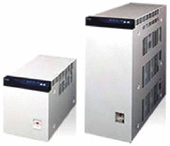
9 is positive. In each combination, the bit inverter that outputs a positive voltage works in such a manner that it discharges energy from a DC capacitor. Conversely, the bit inverter that outputs a negative voltage operates in such a manner that it charges energy into the DC capacitor. By gradationally controlling these two operating modes of charging and discharging, it becomes possible to render the average output power of the bit inverters zero. Table 1 Relationship between total output voltage level and the voltages of bit inverters 2.2 Enhancement of voltage controllability In order to further improve the precision of the output of the gradationally controlled voltage inverter, we have developed a technology with which to further diminish jaggies, or further smoothen the step-like line connecting the individual voltage levels. Figure 3 shows an example of applying this technology to a ternary 4-bit configuration. The DC voltage ratio among bit inverters B1 through B4 stands at 1:1:3:9 and bit inverters B2 through B4 work together to output 13 levels of voltage due to ternary motion. On the other hand, B1 undergoes PWM control in such a manner that it outputs the difference in voltage between the step-like voltage output by bit inverters B2 through B4 and a sinusoidal voltage command. Thanks to this arrangement, it becomes possible to obtain a fine-grained or reasonably clean sinusoidal voltage without the need for increasing the switching frequency of bit inverters B2 through B4 while adding a small filter alone. 3. Example of commercialization of the gradationally controlled voltage inverter 3.1 Gradationally controlled-type voltage sag protector Figure 4 shows the configuration of a gradationally controlled-type binary 4-bit voltage sag protector. The gradationally controlled voltage inverter is inserted in series with the AC line. A series compensation method is adopted where only a shortage in voltage will be compensated for. When AC line power is normal, the relay is closed to bypass the inverter and so reduce losses. In the event of a voltage sag, the relay is opened and the gradationally controlled voltage inverter makes up for any shortage in voltage. Figure 5 shows a voltage waveform that was produced when protection was provided against a 100% voltage sag. The sag protector began operating within 4 ms and demonstrated stable protective action thereafter. Figure 6 shows two voltage sag protectors which we have commercialized. We were able to reduce the volumetric size of these sag protectors to a mere one tenth of that of our conventional UPSs having the same capacity ratings. Furthermore, we have achieved long-duration compensation capability that satisfies the SEMI-F47 Standard Specification for Semiconductor Process Equipment Voltage Sag Immunity. 3.2 Gradationally controlled-type UPS Figure 7 shows the configuration of a UPS employing a ternary 4-bit gradationally controlled voltage inverter. The gradationally controlled voltage inverter consists of a set of three bit inverters that is connected in parallel across the AC line and a bit inverter that is connected in series with the AC line. It is equipped with voltage compensation for when a power failure occurs, voltage regulation in the condition with low or high line voltage and active filtering functions. Fig. 3 High precision voltage control method Fig. 4 Schematic circuit of voltage sag protector Mitsubishi Electric ADVANCE March


10 Input voltage Output voltage 100% voltage sag Figure 8 shows a voltage waveform that is produced by our prototype UPS when the power fails. As can be seen, the series- and parallel-connected bit inverters work in concert as a 4-bit gradationally controlled inverter and thereby generate a high-precision waveform. Fig. 5 Example of compensated waveforms by voltage sag protector Voltage (V) Time (s) Fig. 8 Output waveform of UPS in voltage compensation Fig. 6 Commercialized voltage sag protector Figure 9 shows our commercialized 1.5-kVA gradationally controlled rack-mount-type UPS for which we have achieved an ultraslim housing design measuring a mere 44 mm in thickness. Furthermore, as the insulation transformer found in every conventional UPS is no longer needed and so its excitation loss is eliminated, it is possible to achieve efficiencies of 95% over wide input voltage range. Fig kVA rack-mount UPS Fig. 7 Circuit diagram of UPS using gradationally controlled voltage inverter The gradationally controlled voltage inverter we have developed will bring radical changes to power electronics equipment in the 21st century. 8
11 Electromagnetic Noises from Power Devices and Filter Design Authors: Akinori Nishizawa* and Satoshi Azuma* 1. Introduction Technologies for designing power electronic circuits which are used in everything from industrial and communications equipment to household electrical appliances are an important factor that determines the quality and cost of such products. In recent years, regulations concerning electromagnetic noise (emissions) have been tightened. It has become necessary to obtain the CE marking based on the recommendations of CISPR (Comite international Special des Perturbations Radioelectriques) and other institutions in Europe as well as certification from the FCC (Federal Communications Commission) in North America in order to export products to those regions. Regulations are also being tightened in the Japanese domestic market. Under these circumstances, technologies for determining filter configurations and the like at the design stage by simulating the noise generated by power electronic circuitry have been growing in importance (3) in order to raise the reliability of products yet reduce their cost. Regarding noise filtering technologies, progress is being made in studies of active filters (4), which are configured to generate voltage of opposite phase to cancel out noise, in addition to conventional passive-type filters. 2. Simulation of electromagnetic noise 2.1 Modeling of electromagnetic noise sources The electromagnetic noise generated in power electronic circuits such as inverters is caused by the high-speed switching operation of transistors and freewheeling diodes that are found in those circuits. As an example, a 600V/150A IGBT (insulated-gate bipolar transistor) module's turn-on and turn-off waveforms are shown in Fig. 1. As for the switching operation of recent IGBTs, voltage rise and fall times are on the order of 100 nsec. This means that noise cannot be reduced even by reducing the speed of switching operation, and so noise filter-based measures must be used. On the other hand, where radiated emissions are concerned, since oscillation at the time of reverse recovery of freewheeling diodes can be suppressed by an increase in transistor-driving gate resistance, the radiated emissions are expected to be reduced at the expense of an increase in loss associated with switching. The modeling of such an electromagnetic noise source is important when making predictions about electromagnetic noise in the design stage. Therefore, an analytical model is needed that reflects the features of generating factors for conducted and radiated emissions. (a) Turnn on (b) Turn off Fig. 1 Waveforms of IGBT switching 2.2 Analysis of conducted emissions EMI (electromagnetic interference) emission in inverter equipment is caused by the switching operation of the equipment s power devices. Carrier frequencies are usually on the order of 10 khz. Taking a look at various EMI standards, regulations on conducted EMI emissions often begin at 150 khz, so conducted EMI emissions in the neighborhood of 150 khz should be focused on. Since this 150-kHz band is home to the lower-order harmonics of inverter carrier frequencies, this is where Fourier harmonic components of switching carriers come into direct view and where conducted emissions (noise voltage across terminals) occur with *Advanced Technology R&D Center Mitsubishi Electric ADVANCE March

12 the greatest magnitude. In order to suppress conducted emissions in this band, a noise filter is usually installed. Also, for determining filter specifications, the amount of emissions in this band needs to be estimated. Here, we will consider an inverter equipment whose load is a motor. As for a typical setup for measuring conducted emissions from inverter equipment, the AC line power is connected to the inverter equipment by an LISN (Line Impedance Stabilization Network) (and then through a noise filter) while the load (motor in this case) is connected to the inverter equipment through an output cable. By feeding the output of the LISN into a spectrum analyzer or the like, it is possible to measure conducted emissions. In order to compute conducted emissions in a circuit simulation, it is necessary to prepare an equivalent circuit model that represents a setup like the one mentioned above. Here, the output cable and the load (motor) must be represented by an equivalent circuit that incorporates their impedances with respect to the ground (GND). For the motor, we assumed the equivalent circuit shown in Fig. 2. U V W E Fig. 2 Equivalent circuit for motor Impedance-to-GND and phase characteristics are shown in Fig. 3. The impedance characteristics in Fig. 3 reveal that the motor's impedance with respect to GND manifests itself in the form of capacitive impedance. Since this parasitic capacitance represents the stray capacitance between the motor's windings and stator (motor housing), it can be estimated from the construction/structure of the motor. At frequencies above 100 khz, a plurality of resonance modes occur. In this region, the impedance characteristics of the motor windings themselves have a considerable impact. To express such characteristics that show up as being capacitive (between the windings and the housing) at lower frequencies and appear in the form of multiple resonance modes at higher frequencies, we assumed the equivalent circuit shown in Fig. 2. We confirmed that this equivalent circuit represented a model capable of accurately mimicking actual measurement results as shown in Fig. 3. Impedance (ohm) Phase(degree) Mesurements Equivalent Circuit Frequency(kHz) 0 (a) Impedance Mesurements Equivalent Circuit Frequency(kHz) (b) Phase Fig. 3 Characteristics of impedance and phase for motor By using a motor model like the one described above and by translating the AC line power, a LISN, noise filter, an inverter drive block and an output cable into respective models, it is possible to perform conducted-emissions computations in the circuit simulation. The results of conducted-emissions computations performed in the 150-kHz band with the output cable length as a parameter and the results of actual measurements are shown in Fig. 4. At each cable length, the analytical result agreed well with the actual measurement result, to within a few db. Although there was virtually no difference among the shorter cable lengths of 2m, 5m and 8m in the magnitude of conducted emissions, there were increases of 10 db or greater in magnitude with 50-meter and shielded 30-meter cables. These outcomes can be interpreted to mean that the magnitude of conducted emissions depends on the motor at the shorter cable lengths of 2m, 5m and 8m while the magnitude of conducted emissions is determined by the cable length for the longer 50-meter and (shielded) 30-meter cables. Since the motor's impedance with respect to GND is determined by the construction of the motor, this motor construction is an important factor when considering EMI noise. Incidentally, the cable impedance with respect to GND can be approximated from the construction and length of the cable. Note that when a shielded cable is used, its impedance with respect to GND becomes 10
13 smaller because of its shielding metal, and conducted emissions become greater in magnitude when compared with its unshielded counterpart. As has been discussed, since the magnitude of conducted emissions depends on the impedances of the inverter equipment's cable and load with respect to GND, it is necessary to consider the impedances of the cable and load with respect to GND. This will enable conducted emissions of particular inverter equipment to be calculated. Based on the results of the calculations, it then becomes possible to design noise filters to keep EMI within specification and also to estimate the impact of extending the cable length. Conducted emission(db) Measurements Computed results 2m 5m 8m 50m 30m (Shielded) Cable length(m) Fig. 4 Conducted emission for cable length 3. Designing noise filters 3.1 Passive noise filters For inverter equipment, noise filters are virtually indispensable in view of the EMI standards. Passive-type noise filters are generally made up of common-mode coils, capacitors to be connected to GND, and capacitors to be placed across phases. The amount of filter-induced attenuation is determined by the characteristics of those components. While a filter is still at the design stage, it is natural to theoretically secure the desired amount of attenuation. However, this alone does not suffice and it is necessary to pay attention to (1) installation positions, (2) magnetic saturation of coil cores, (3) leakage current, and the like. When a common-mode coil, which is made by winding a large number of turns onto a small core, is used, the core can go into magnetic saturation. Therefore, it is necessary to estimate the magnitude of common-mode current that can occur and decide upon a core size and the number of winding turns so as to avoid saturation. Furthermore, since such a noise filter is made up of LC circuitry, it has a resonant frequency. If this resonant frequency coincides with a carrier frequency, a high common-mode current will be produced, so care is required. Moreover, regarding the magnetic fluxes produced by coil cores, often only those fluxes that are generated by common-mode current are considered. However, magnetic flux is also generated by normal-mode (commercial frequency) current on account of leakage inductance. Since the normal mode has a large current value, for the flux that will develop in the coil core, it is necessary to predict the saturation strength based on the flux amount determined by combining common-mode-induced flux and normal-mode-induced flux. There is also another means by which capacitance with respect to GND is increased in order to provide added attenuation. However, since augmenting the capacitance increases low-frequency leakage current, it is necessary to decide the capacitor capacitance with a sufficient allowance to avoid problems by considering the configuration of a given commercial power supply. Furthermore, the leakage current is greatly impacted by the impedance of the load (for example, motor) with respect to GND in addition to the capacitance with respect to GND. Caution is required because, when a load having a small impedance (or a large parasitic capacitance) is installed, the load will give rise to a greater leakage current than ground-connected capacitors would do. 3.2 Active noise filters A typical technique for reducing electromagnetic noise is to connect a passive filter, but this inevitably increases the overall volume and cost of a given inverter system. There are also problems of resonance that occurs between reactors and capacitors making up a passive filter as well as magnetic saturation in the cores of such reactors. Therefore, we propose active noise filtering that is characterized by its ability to reduce both normal-mode and common-mode conducted emissions, eliminates the need for a common-mode transformer, and makes it possible to reduce the breakdown voltage of transistors that are active elements (meaning that transistors with lower breakdown voltages may be used). An active noise filter is designed to directly detect conducted emissions and perform feedback control on output current for each individual phase with the help of transistor circuitry so as to reduce those conducted emissions to zero. Figure 5 shows a per-phase block diagram of an active noise filter, where CNV, INV and IM represent a rectifier, an inverter and an induction motor, respectively. Here, high-frequency voltage vc y that appears across parasitic capacitance C y existing along an AC line cable and the like corresponds to conducted emissions observed by an LISN. Therefore, to suppress this high-frequency voltage vc y, the active filter has the following functions: Detection of voltage vc y across C y Extraction of high-frequency voltage components (150 khz and above, for example) by the high-pass filter (HPF) as conducted emissions to be suppressed Mitsubishi Electric ADVANCE March
14 Creation of current command i com * with proportional gain K so that the above high-frequency voltage components become zero Conversion of voltage signal i com * to current i com by means of ±15V-powered voltage-to-current conversion circuitry (V-to-I Conv.) and injection of i com into C y through capacitor C in. Fig. 5 Block diagram of active noise filter The results of conductive-emissions measurements performed on an inverter in operation with the help of an LISN are shown in Fig. 6. Since the AC line power used represents a 3-phase input, we connected the per-phase functional block shown in Fig. 5 to each of the three phases. The active noise filter provided an attenuation of approximately 20 db in the neighborhood of 150 khz as intended by its design which we developed using a Bode diagram. For conducted emissions in MHz bands, they can be reduced by connecting separate phase-to-phase capacitors. We have started making verification studies of optimum designs, each employing active noise filtering and simple passive noise filtering. 4. Conclusion In this paper, we have discussed our technologies for embodying power electronics circuitry and noise (emission) propagation into models and design noise filters. By building everything, from the inverter circuit and cable to the motor that acts as a load, into an equivalent circuit model, it becomes possible to make quantitative EMI-emissions assessments of arbitrary combinations of those models. Thanks to these technologies, it has now become possible to select filter constants and create a design from the drawing stage, thus shortening development times and reducing cost. We are also forging ahead with the commercialization of a more adaptive filtering technology like the one embodied in active filters. References (1) R. Rohrer, L. Nagel, R. Meyer and L. Weber, Computationally efficient electronic-circuit noise calculations, IEEE Journal of Solid-State Circuits, Vol. SC-6, No. 4, 1971 (2) L. Nagel, SPICE2: A Computer Program to Simulate Semiconductor Circuits, Ph.D. dissertation, University of California at Berkeley, (3) A. Nishizawa, S. Tanabe and M. Nakanishi, Switching interference from power electronics-applied devices, J. IEIE Jpn. Vol. 24, No. 4, pp , 2004 (4) S. Azuma and M. Kimata, Active noise filter to reduce normal-mode and common-mode conducted EMI noise, IEEJ Trans. IA, Vol. 124, No. 9, pp , 2004 dbµ[v] Without active noise filter With active noise filter Fig. 6 Measurements of conducted emission [Hz] 12
15 Evaluation of Fatigue Life Reliability and New Lead Bonding Technology for Power Modules Authors: Toshihiro Matsunaga* and Shingo Sudo** The authors have developed a fast thermal cycling test method of evaluating the reliability of power modules. The method shortens the time required for a life evaluation test of Al wire bond lift-off to one-quarter of the conventional power cycling test method. The authors have also developed a technology for Cu lead interconnection structures that can be applied for higher current densities of chips and improved productivity, replacing the current Al wiring method. Case Si Chip Al wire 1. Introduction Power modules, which are used for an increasingly wide range of industrial applications, are used not only for inverter control of household electric appliances but also for high power applications that include automobiles, electric railroads, and electric power. Today s power modules require far greater reliability with respect to electric performance, insulation efficiency, thermal performance, and strength, and so it is expected that the specifications of such modules will improve. It has also become necessary to rapidly develop and commercialize products of low cost and high reliability. To meet these requirements, we have to improve the accuracy and speed of reliability evaluation techniques and develop products based on new technological concepts. This paper deals with two types of technology. The first one is a technology for quickly evaluating the thermal fatigue wire lift-off life of Al wire bond used for the main electrode interconnections in power modules, as a means of evaluating the strength reliability for power module wiring structures. The second technology is related to a wiring structure with thin Cu lead as a new bonding method that supersedes the conventional wire bonding method and meets the future needs for high current densities. 2. Strength Reliability Evaluation Technology (Accelerated Testing Technology for Wire Lift-off Life) The ultrasonic Al wire bonding method is widely used for electric wiring of Si chips in power module. Fig. 1 shows a cross-sectional view of a power module employing this method. Solder Base plate Ceramic substrate Fig. 1 Cross-sectional view of power module Since the wire bonds are subjected to cyclic thermal fatigue due to the fall and rise in temperature of the chips which often results in fatigue damage, it is necessary to accurately grasp the fatigue characteristics of wire bonds. In the conventional methods of reliability testing, power cycling tests are conducted, while current is actually supplied and disconnected to/from the power modules, but this is extremely time-consuming. The authors have developed a method for rapidly evaluating thermal fatigue life (fast thermal cycling test method) in which only Al wire bonded chip sections are sampled and thermal stress equivalent to that generated in the power cycling procedure is applied by external heating, as an alternative to the conventional power cycling test method. Fig. 2 shows the section evaluated in the fast thermal cycling test method. Since fast heating and cooling are involved in the test, the testing equipment uses a high-performance ceramic heater and a heat sink. In addition, a high-precision temperature controller is used for transient temperature changes due to cyclic heating and cooling. Fig. 3 shows an example of the temperature swing for T = 100 K. Temperature control for a thermal cycle of about 2 seconds (per cycle) is possible. Compared with the period required in the conventional power cycling test method, life of wire bond can be evaluated in about one-quarter of the time. *Advanced Technology R&D Center **Manufacturing Engineering Center Mitsubishi Electric ADVANCE March

 Heat sink Ceramic heater Fig. 2 Photograph of fast thermal cycling test Fig. 3 Profile of temperature swing ( T = 100 K) Fig.")

16 Si Chip Al wire TECHNICAL REPORTS The authors have thus confirmed that the new fast thermal cycling test method can evaluate the life of wire bond lift-off more quickly than the conventional method, without having to prepare actual modules. The new test method will enable the influence of chip specifications and wire bonding conditions to be evaluated more quickly and so greatly speed up product development. Temperature ( C) Heat sink Ceramic heater Fig. 2 Photograph of fast thermal cycling test Fig. 3 Profile of temperature swing ( T = 100 K) Fig. 4 shows the results of evaluating the influence of the thermal cycle temperature range T (50 to 100 K with a minimum junction temperature of T min = 25 C) on the life of wire bond lift-off in the fast thermal cycling test. The values indicated agree well with the results of life obtained by the power cycling test conducted by Cova et al. (1) Number of cycles to failure, Nf (cycles) Temperature range T(K) Fig. 4 Relation between number of cycles to failure and T 3. Bonding Technology (Cu lead interconnection structure) With the recent developments of power semiconductor chips, chips of higher current densities with reduced areas required for a fixed current value are common today. As a result, the conventional wire bonding method is reaching its limit for the capacity of feeding current through wires. Besides, in the case of a power module of several hundred amperes, the module requires a huge number of Al wires which reduces productivity, so new interconnection techniques are needed to replace the conventional Al wire interconnection method. Several methods have been proposed, including the metal post structure method that employs flip-chip bonding (2). Mitsubishi Electric Corporation is developing a new wiring structure that will meet the future needs for high current densities of chips as well as improved productivity for similar module configurations as the current Al wire bonded devices. That is, the structure will replace the Al wire interconnection on the chip for high current power modules, with Cu lead interconnection in which the Cu lead is placed on the chip by soldering. Power modules require high reliability and thermal cycle performance due to the environments in which they are used. There is a concern that lead interconnection methods may deteriorate the electrical characteristics due to damage to the soldered junctions by thermal cycling. Therefore, we conducted a thermal cycling test of a lead bond module to identify the changes in characteristics. Fig. 5 shows a photo of a power MOSFET chip having an edge of 12 mm and a thickness of 0.3 mm with Al wiring. Fig. 6 shows a photo of the same MOS- FET chip with Cu lead bonded. A cross-sectional view of the lead bond module is shown in Fig. 7. The Al wire bond module has 16 wires of φ = 400 µm on the chip. The lead interconnection has a Cu plate having a thickness of 0.2 mm and a width of 11 mm on the chip, which are bonded with Sn-Ag-Cu solder having a thickness of about 0.1 mm. For thermal cycling, a range between 40 C and +125 C (10 minutes respectively) is used. For the intermediate measurement, the on-state resistance (R DS (ON) ) of the MOSFET chip was measured to check the deterioration of module characteristics. 14

 /mω 4.00 3.00 2.")


17 MOSFET Chip Al wire (φ=400µm) Fig. 5 Top view of the chip in the wire bond module MOSFET Chip tooth portion having the same thickness, so that the rigidity of the lead at the solder-bonded junction could be lowered to effectively reduce the strain in the solder caused by the difference in coefficient of thermal expansion. Fig. 9 shows a photo of a comb-shaped lead interconnection. The comb teeth are formed such that they cover eight areas divided by the gate interconnection on the chip and are fixed by soldering. The width of each comb tooth is 0.8 mm. R DS(ON) /mω Open LEAD WIRE Ni-plated Cu lead (t=0.2mm) Cycles Fig. 8 Transition of on-state resistance in the thermal cycling test, comparing the lead bond with the wire bond MOSFET Chip Fig. 6 Top view of the chip in the lead bond module MOSFET Chip Cu lead (t=0.2mm) Ceramic substrate Pb-free solder Fig. 7 Cross-sectional view of the lead bond module Fig. 8 shows the number of cycles in the thermal cycling test and the transition of R DS (ON). With the wire bond structure, the resistance did not show changes up to 3000 cycles, while the lead bond interconnection showed an increase in resistance of approximately 1.5 times at 1000 cycles; it propagated a crack fully through the solder between the chip and lead after 2000 cycles, and finally open-circuit occurred. A crack in the solder propagates due to the strain in the solder layer resulting from the difference in coefficient of thermal expansion of Si chip and Cu lead. Reducing the strain in solder is an effective way of preventing the crack growth. Cracks may also be prevented by reducing the rigidity of the lead by using thinner leads, although this may increase the overall resistance of the interconnection. Therefore, we decided to use a lead shape that has a comb-shaped bonding area on the chip, with each split Ni-Plated Cu comb-shaped lead (t=0.2mm) Fig. 9 Top view of the chip in the comb lead bond module The authors also confirmed the transition of R DS (ON) of the comb-lead interconnection modules in a thermal cycling test with a temperature range of 40 C through +125 C. Fig. 10 shows the number of cycles and the transition of R DS (ON). R DS(ON) /mω COMB-LEAD WIRE Cycles Fig. 10 Transition of on-state resistance under the thermal cycling test, comparing the comb lead bond with the wire bond Mitsubishi Electric ADVANCE March
18 The thermal cycling test clearly shows that the comb-shaped lead interconnection structure can keep the increase in R DS (ON) beyond 1000 cycles. Furthermore, the structure does not suffer an open-circuit at 3000 cycles, with the increase in R DS (ON) suppressed to around 10%. 4. Conclusion The authors have developed and confirmed the effectiveness of a fast thermal cycling test method for evaluating the life of Al wire bond lift-off more quickly than the conventional method, for evaluating the reliability of power modules. The authors have also proposed a Cu lead interconnection structure as a new interconnection method and proved that use of the comb-shaped lead divided into teeth is effective in preventing cracks in the solder used to bond the chip and lead under thermal cycling conditions. References: (1) P. Cova and F. Fantini, On the effect of power cycling stress on IGBT modules, Microelectronics Reliability 38, (1998), pp (2) X. Liu and G. Lu, Power Chip Interconnection: From Wire Bonding to Area Bonding, IMAPS2000, Boston, (2000), pp
19 SiC Devices and Their Application Technologies Authors: Shin-ichi Kinouchi* and Masayuki Imaizumi* Semiconductor silicon carbide (SiC) is expected to be the promising material for next-generation power devices. However, since crystal growth techniques and device process techniques are still immature, SiC devices sufficient for practical use have not yet been developed. Mitsubishi Electric Corporation has been actively developing fundamental SiC technologies, and prototypes of 10 A-class devices are now being manufactured in order to achieve practical applications. 1. Manufacture and Electrical Static Characteristics of SiC-MOSFET The size of the unit cell of the SiC-metal oxide semiconductor field effect transistor (MOSFET) experimentally manufactured this time is 25x25 µm with a gate length of 2 µm. Two types of MOSFET prototype with an active area per chip of 0.88 mm 2 and 7.8 mm 2 were manufactured. These are respectively equivalent to 1 A-class and 10 A-class current ratings. Their substrates are 4H-polytype n-type SiC. A drift layer with a donor density of 1x10 16 cm -3 and a thickness of 12 µm was prepared by epitaxial growth. The well region and JTE (junction termination extension) region were implanted with Al ions as p-type dopant and subjected to activation annealing in pressure-reduced Ar atmosphere. After removing the surface layer formed by activation annealing, an n-type channel layer was formed by epitaxial growth. The thickness and density of this particular channel layer were set so as to ensure that the whole layer would be depleted through pn junction with the p-type well layer. The gate oxide film was formed by thermal oxidation in a steam and oxygen atmosphere. The gate electrode was poly-si doped with P. After interlayer dielectrics were deposited, the metallic electrodes of source, drain, and gate were formed. Fig. 1 shows typical drain current and drain voltage characteristics (ON characteristics) of the 1 A-class SiC prototype. A specific ON-resistance of 12.9 mωcm 2 resulted from a gate voltage of 12 V (field intensity in the gate oxide film: 3 MV/cm) and a current density of 50 A/cm 2. For comparison with Si, the value at this particular current density is taken. Fig. 2 shows the blocking characteristics (OFF characteristics) of the MOSFET shown in Fig. 1. Although there is a leakage current from the MOS channel section at a gate voltage of 0 V, an avalanche breakdown voltage of 1.2 kv or more results. The current values remain unchanged at gate voltages lower than 5 V (due to the absence of channel leakage current). The threshold voltages of the MOSFET manufactured experimentally this time range from approximately 0.5 V to 0.5 V and tend to lower as the ON-resistance is reduced. A gate voltage lower than 5 V is necessary to surely turn the MOSFET off; Drain current (A) Drain current (A) Drain voltage (V) Fig. 1 1 A-class SiC-MOSFET drain current vs. drain voltage Drain voltage (V) Fig. 2 Blocking characteristics of 1 A-class SiC-MOSFET *Advanced Technology R&D Center Mitsubishi Electric ADVANCE March

20 threshold voltage control is to be addressed from now on. As for a 10 A-class MOSFET, an ON-resistance of approximately 20 mωcm 2 resulted and a blocking voltage of approximately 1.2 kv or higher was obtained at a gate voltage of 5 V. 2. Motor Operation by SiC Module SiC inverter modules were manufactured by combining the 1 A-class SiC-MOSFETs and SiC-Schottky barrier diodes (SBD), using an Si-IGBT module package for a rating of 1200 V/10 A. This package is an existing one, prepared for experimental purposes, and is not optimum for SiC applications. Fig. 3 shows the inverter circuit for motor operation using a 1 A-class SiC-inverter module and output current waveforms of the inverter. The motor employed in this case is a 0.1-kW (3-phase) geared motor. The operation conditions include Vcc = 200 V, Irms = 0.3 A, a fundamental frequency of 60 Hz, and a carrier frequency of 4.5 khz. The motor operated normally without any change in device characteristics after about 80 hours of continuous operation. The authors will continue to evaluate changes in device characteristics over time and the reliability. 3. Evaluation of Transient Characteristics of SiC Devices A chopper circuit module was manufactured by combining the 10 A-class SiC-MOSFET and SiC-SBD for evaluating the transient characteristics of SiC devices. The double-pulse method was used for evaluating the transient characteristics. For comparison, a chopper circuit module including an Si-insulated gate bipolar transistor (IGBT) with a rating of 1200 V/10 A and an Si-PiN diode in the same package as the SiC module was evaluated. Fig. 4 shows the turn-on transient waveforms of the switching FETs (transistors), while Fig. 5 presents the turn-off transient waveforms. The measurement conditions were a DC voltage of 600 V, a load current of 11 A, and a module temperature of 125 C. Fig. 4 Turn-on transient waveforms of the switching FETs Fig. 3 Inverter circuit for motor operation using SiC-inverter modules (top), and output current waveforms of the inverter (bottom) MOSFET, IGBT Current[A] MOSFET, IGBT Voltage[V] SiC- MOSFET Si- CSTBT 0.2 Turn-off Transient Tj=125 Rg_SiC=47Ω, Rg_Si=47Ω Vpn=600V, IL=11A Si-CSTBT SiC-MOSFET Eoff_SiC=0.17mJ Eoff_Si=1.21mJ Time [s] x10-6 Fig. 5 Turn-off transient waveforms of the switching FETs 18
21 For the comparison of the turn-on waveforms between SiC-MOSFET and Si-IGBT, gate resistances that result in the same turn-on di/dt with both Si module and SiC module were used. For the comparison of the turn-off waveforms between SiC-MOSFET and Si-IGBT, a gate resistance that results in the same surge voltage with both Si module and SiC module was used. The gate resistance used in turn-on was 20 Ω with the SiC-MOSFET and 47 Ω with the Si-IGBT. On the other hand, the gate resistance used in turn-off was 47 Ω with the SiC-MOSFET and 47 Ω with the Si-IGBT. Fig. 4 clearly indicates that the difference in the reverse recovery behavior of the diodes had a great influence on the turn-on loss. Recovery current slightly higher than 2 A due to the extension of the depleted region of SiC-SBD is observed in the SiC module, but it is far lower than the recovery current of the Si-PiN diode. Fig. 5 shows clearly that there is a big difference in the tail current values of the switching transistors. Since the SiC-MOSFET is a unipolar device, no carrier storage is present at the turn-off moment and no tail current is generated in principle. Comparison of the transient loss between the SiC module and Si-IGBT module under the measurement conditions mentioned above reveals that the turn-off loss of the SiC module is 0.60 times that of the Si module, the turn-on loss is 0.14 times, and the diode recovery loss is 0.02 times. 4. Trial Calculation of Inverter Operation Loss Based on the transient characteristics and static characteristics of the SiC devices used in this study, the loss during the operation of the 3-phase pulse width modulation (PWM) inverter was calculated. The conditions used in the loss calculation include a module temperature of 125 C, a DC voltage of 600 V, a phase current of Irms = 3.5 A, a carrier frequency of 10 khz, a PWM modulation ratio of 1.0, and a power factor of 0.8. Comparing the SiC inverter with the Si inverter, the transient loss (turn-on + turn-off + recovery) of the SiC inverter was reduced to 23% that of the Si inverter, proving that the total loss of the inverter can be reduced to 44%. We will continue to improve the performance and reliability of SiC-MOSFETs and SiC-SBDs with a view to using SiC modules in practical applications. Part of this study was conducted under a joint research contract with the New Energy and Industrial Technology Development Organization (NEDO) as one of the Strategic Development of Technology for Efficient Energy Utilization financed by a subsidy from the Ministry of Economy, Trade and Industry. Mitsubishi Electric ADVANCE March
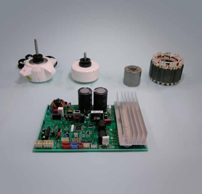
22 Technologies of Power Electronics for Air Conditioner and Household Electric Appliances Authors: Mamoru Kawakubo* and Masaaki Yabe* Household electric appliances such as air conditioners and refrigerators are commonly equipped with inverters that make extensive use of power electronics technologies. The power electronics technologies developed for conserving energy and resources have helped greatly reduce power consumption as well as the amount of materials used for construction. This paper reviews the technologies used to improve the operation efficiency and resource saving effects of brushless DC motors and the inverters to dive the motors. 1. Technologies for Improving Efficiency of Inverters Used in Compressors The inverters installed in air conditioners or refrigerators efficiently drive brushless DC motors for compressors. The environment within compressors is subject to high temperature and high pressure conditions and it is very difficult to install position sensors for detecting the magnetic poles of rotors inside. In other words, a position-sensorless driving method is essential. The conventional brushless DC motors are driven by rectangular-wave inverters for ease of control, but the many harmonics contained in the motor current cause iron loss or great torque ripple. To solve this problem, we have developed a sine-wave inverter and installed it in air conditioners, refrigerators, and other electric appliances. The inverter is installed in a vector control feature and the motor is driven synchronously. Fig. 1 shows the control block diagram. This control method employing a frequency compensator maintains stable rotational speed in spite of fluctuations in load torque of the motor, thus reducing the arithmetic load for control. Reference Speed Frequency Compensator Controller Reference Voltage Calculator Reference Voltage Coordinates Transformation dt Coordinates Transformation Voltage Limit DC Voltage Sensing Current Fig. 1 Sine wave control block diagram PWM Inverter IPM MOTOR The inverter is required to drive the compressor motor over a wide range of speed, from low speed to high speed, and must drive the motor very efficiently particularly in the middle- and low-speed ranges where the duration of operation is long. To meet this requirement, we have developed an over-modulation system to drive the motor efficiently. Over-modulation PWM (Pulse Width Modulation) can increase the first harmonic output voltage since it can control part of the PWM 100% duty. With the output voltage increased by up to approximately 10%, it is possible to drive high-voltage type motors, which can be designed for lower motor current levels than low-voltage type motors. Consequently, the copper loss of the motor and iron loss of the switching device are reduced, thus improving the efficiency of the motor and the inverter. Compressor motors are subjected to a peak current relative to the fluctuation of the load torque, which causes a large loss. Fig. 2 (a) shows the motor current waveform containing the peak current. We developed a constant torque control technique that maintains the motor output torque at a fixed level. This technique can control the output voltage and frequency of the inverter, enabling the motor output torque to be kept constant. Fig. 2 (b) shows the current waveform when the peak current is controlled. The figure shows that the peak current is reduced by almost half. Refrigerators are equipped with reciprocating compressors, which improve the total efficiency during low-speed operation by up to 4% compared to the conventional control method. Efficiencies have been improved also with rotary-type compressors installed in air conditioners. The efficiencies vary with the motor torque levels and motor characteristics. Next, we developed a maxi- (a) Peak current control Nothing (b) Peak current control Fig. 2 Motor current waveform *Living Environment Systems Laboratory 20


 type rotors housed inside the rotors for their performance and manufacturing specifications.")
23 mum efficiency control technique for efficiently operating motors of different torque levels and characteristics. This technique controls the inverter output voltage to minimize the current on the basis of the motor current value and motor parameters. With this control technique, the motor efficiency of packaged air conditioners during low-speed operation is increased by up to 6%. 2. Technologies for Improving Efficiency of Brushless DC Motors Used in Compressors It is necessary to reduce copper loss and iron loss and downsize the brushless DC motors in order to improve their operation efficiency and conserve resources. Basically, brushless DC motors are equipped with interior permanent magnet (IPM) type rotors housed inside the rotors for their performance and manufacturing specifications. The motor torque of a brushless DC motor is given by Equation (1) below. The first term on the right of the equation represents the magnet torque, while the second term indicates the reluctance torque. T m m { Φ i + ( L L ) i i } = P...(1) f q d where, T m = motor torque, i d = d-axis component of motor current, i q = q-axis component of motor current, L d : d-axis inductance, L q = q-axis inductance, φ f = magnetic flux linkage, and P m = pole pairs. The brushless DC motor we have developed has an even magnetic flux density with rare-earth magnet in an optimum location and is equipped with six poles (the number of poles is increased from four poles) resulting in a thinner stator. The stator employs the concentrated winding method as well as a new core construction called Poki Poki Core. The coil can be wound with the stator core opened. As the length of the coil can be reduced, the coil resistance is reduced while the coil space factor is increased. This new manufacturing method greatly improves the efficiency. Fig. 3 shows the appearances of the motors using a rare-earth magnet and ferrite magnet, respectively. Fig. 4 compares the characteristics of these compressor motors. The newly-developed motor is about 1% more efficient than the conventional motors, while its volume and weight are reduced by about 40% and 35%, respectively, thus saving resources. q d q 3. DC Fan Motors The indoor and outdoor units of air conditioners are equipped with high-efficiency brushless DC motors to reduce power consumption. The rotors are constructed with surface permanent magnets (SPM) which are located on the surface of the rotors. The generated torque is equal to the magnet torque, having no reluctance torque that causes vibration or noise. To reduce noise in the motor, a plastic magnet of high moldability is used for the rotor. The new core structure called Poki Poki Core and the concentrated winding method for the stator result in improved motor performance. Fig. 5 shows photos of the DC fan motors used for indoor units and outdoor units, respectively. Ratio [%] Rare metal magnet type Total Efficiency Fig. 3 Motor Ferrite Magnet Type Sintering ferrite magnet type Volume Fig. 4 Comparison of motor For indoor unit Fig. 5 DC fan motor Rare-earth Magnet Type For outdoor unit Weight DC fan motors are commonly installed in indoor units where space is limited. This is why we used small electronic elements to downsize the inverters in motor. The stator containing the inverter is in a resin housing, allowing the heat from the semiconductor power device to be dissipated via the resin, without the need for fins. Meanwhile, the DC fan motors installed in outdoor units are designed to run quietly and efficiently from low to high speed. Since the motors must operate in sync with external wind, position sensors to detect the rotor magnetic poles are installed in the motors. The invert- Mitsubishi Electric ADVANCE March
Some Key Researches on SiC Device Technologies and their Predicted Advantages
 18 POWER SEMICONDUCTORS www.mitsubishichips.com Some Key Researches on SiC Device Technologies and their Predicted Advantages SiC has proven to be a good candidate as a material for next generation power
Modeling of Conduction EMI Noise and Technology for Noise Reduction
 Modeling of Conduction EMI Noise and Technology for Noise Reduction Shuangching Chen Taku Takaku Seiki Igarashi 1. Introduction With the recent advances in high-speed power se miconductor devices, the
All-SiC Modules Equipped with SiC Trench Gate MOSFETs
 All-SiC Modules Equipped with SiC Trench Gate MOSFETs NAKAZAWA, Masayoshi * DAICHO, Norihiro * TSUJI, Takashi * A B S T R A C T There are increasing expectations placed on products that utilize SiC modules
T-series and U-series IGBT Modules (600 V)
") T-series and U-series IGBT Modules (6 V) Seiji Momota Syuuji Miyashita Hiroki Wakimoto 1. Introduction The IGBT (insulated gate bipolar transistor) module is the most popular power device in power electronics
T-series and U-series IGBT Modules (6 V) Seiji Momota Syuuji Miyashita Hiroki Wakimoto 1. Introduction The IGBT (insulated gate bipolar transistor) module is the most popular power device in power electronics
CHAPTER 1 INTRODUCTION
 1 CHAPTER 1 INTRODUCTION 1.1 GENERAL Induction motor drives with squirrel cage type machines have been the workhorse in industry for variable-speed applications in wide power range that covers from fractional
Latest Control Technology in Inverters and Servo Systems
 Latest Control Technology in Inverters and Servo Systems Takao Yanase Hidetoshi Umida Takashi Aihara. Introduction Inverters and servo systems have achieved small size and high performance through the
Fig. 4. Modeling structure of the evaluation system. rating is tri-phase 400V rms and 10 kw. B. Composition of a main circuit Main circuit composition
 EMI prediction method for SiC inverter by the modeling of structure and the accurate model of power device Sari Maekawa, Junichi Tsuda, Atsuhiko Kuzumaki, Shuhei Matsumoto, Hiroshi Mochikawa TOSHIBA CORPORATION
Conventional Single-Switch Forward Converter Design
 Maxim > Design Support > Technical Documents > Application Notes > Amplifier and Comparator Circuits > APP 3983 Maxim > Design Support > Technical Documents > Application Notes > Power-Supply Circuits
CHAPTER 2 CURRENT SOURCE INVERTER FOR IM CONTROL
 9 CHAPTER 2 CURRENT SOURCE INVERTER FOR IM CONTROL 2.1 INTRODUCTION AC drives are mainly classified into direct and indirect converter drives. In direct converters (cycloconverters), the AC power is fed
PIEZOELECTRIC TRANSFORMER FOR INTEGRATED MOSFET AND IGBT GATE DRIVER
 1 PIEZOELECTRIC TRANSFORMER FOR INTEGRATED MOSFET AND IGBT GATE DRIVER Prasanna kumar N. & Dileep sagar N. prasukumar@gmail.com & dileepsagar.n@gmail.com RGMCET, NANDYAL CONTENTS I. ABSTRACT -03- II. INTRODUCTION
Power Semiconductor Devices
 TRADEMARK OF INNOVATION Power Semiconductor Devices Introduction This technical article is dedicated to the review of the following power electronics devices which act as solid-state switches in the circuits.
4H-SiC V-Groove Trench MOSFETs with the Buried p + Regions
 ELECTRONICS 4H-SiC V-Groove Trench MOSFETs with the Buried p + Regions Yu SAITOH*, Toru HIYOSHI, Keiji WADA, Takeyoshi MASUDA, Takashi TSUNO and Yasuki MIKAMURA ----------------------------------------------------------------------------------------------------------------------------------------------------------------------------------------------------------------------------------------------------------
MODELLING AND SIMULATION OF DIODE CLAMP MULTILEVEL INVERTER FED THREE PHASE INDUCTION MOTOR FOR CMV ANALYSIS USING FILTER
 MODELLING AND SIMULATION OF DIODE CLAMP MULTILEVEL INVERTER FED THREE PHASE INDUCTION MOTOR FOR CMV ANALYSIS USING FILTER Akash A. Chandekar 1, R.K.Dhatrak 2 Dr.Z.J..Khan 3 M.Tech Student, Department of
INTRODUCTION TO MOS TECHNOLOGY
 INTRODUCTION TO MOS TECHNOLOGY 1. The MOS transistor The most basic element in the design of a large scale integrated circuit is the transistor. For the processes we will discuss, the type of transistor
High-power IGBT Modules
 High-power IGBT Modules Takashi Nishimura Yoshikazu Takamiya Osamu Nakajima 1. Introduction To help curb global warming, clean energy, rather than fossil fuels, has been used increasingly in recent years.
Determination of EMI of PWM fed Three Phase Induction Motor. Ankur Srivastava
 Abstract International Journal of Technical Innovation in Modern Engineering & Science (IJTIMES) Impact Factor: 3.45 (SJIF-2015), e-issn: 2455-2584 Volume 3, Issue 05, May-2017 Determination of EMI of
Simulation Technology for Power Electronics Equipment
 Simulation Technology for Power Electronics Equipment MATSUMOTO, Hiroyuki TAMATE, Michio YOSHIKAWA, Ko ABSTRACT As there is increasing demand for higher effi ciency and power density of the power electronics
(a) All-SiC 2-in-1 module
 All-SiC 2-in-1 module") All-SiC -in- Module CHONABAYASHI, Mikiya * OTOMO, Yoshinori * KARASAWA, Tatsuya * A B S T R A C T Fuji Electric has developed an utilizing a SiC device that has been adopted in the development of a high-performance
All-SiC -in- Module CHONABAYASHI, Mikiya * OTOMO, Yoshinori * KARASAWA, Tatsuya * A B S T R A C T Fuji Electric has developed an utilizing a SiC device that has been adopted in the development of a high-performance
UNIT 3: FIELD EFFECT TRANSISTORS
 FIELD EFFECT TRANSISTOR: UNIT 3: FIELD EFFECT TRANSISTORS The field effect transistor is a semiconductor device, which depends for its operation on the control of current by an electric field. There are
OUTLINE. Introduction. Introduction. Conducted Electromagnetic Interference in Smart Grids. Introduction. Introduction
 Robert Smoleński Institute of Electrical Engineering University of Zielona Gora Conducted Electromagnetic Interference in Smart Grids Introduction Currently there is lack of the strict, established definition
About the High-Frequency Interferences produced in Systems including PWM and AC Motors
 About the High-Frequency Interferences produced in Systems including PWM and AC Motors ELEONORA DARIE Electrotechnical Department Technical University of Civil Engineering B-dul Pache Protopopescu 66,
Automotive EMC. IEEE EMC Society Melbourne Chapter October 13, 2010 By Mark Steffka IEEE EMCS Distinguished Lecturer
 Automotive EMC IEEE EMC Society Melbourne Chapter October 13, 2010 By Mark Steffka IEEE EMCS Distinguished Lecturer Email: msteffka@ieee.org IEEE 1 Automotive Systems Past and Present Today s vehicles
Solution of EMI Problems from Operation of Variable-Frequency Drives
 Pacific Gas and Electric Company Solution of EMI Problems from Operation of Variable-Frequency Drives Background Abrupt voltage transitions on the output terminals of a variable-frequency drive (VFD) are
Automotive Systems Past and Present
 Automotive EMC IEEE EMC Society Eastern North Carolina Section February 9, 2010 By Mark Steffka IEEE EMCS Distinguished Lecturer Email: msteffka@ieee.org IEEE 1 Automotive Systems Past and Present Today
Fig. 1 - Enhancement mode GaN has a circuiut schematic similar to silicon MOSFETs with Gate (G), Drain (D), and Source (S).
, Drain (D), and Source (S).") GaN Basics: FAQs Sam Davis; Power Electronics Wed, 2013-10-02 Gallium nitride transistors have emerged as a high-performance alternative to silicon-based transistors, thanks to the technology's ability
GaN Basics: FAQs Sam Davis; Power Electronics Wed, 2013-10-02 Gallium nitride transistors have emerged as a high-performance alternative to silicon-based transistors, thanks to the technology's ability
LM125 Precision Dual Tracking Regulator
 LM125 Precision Dual Tracking Regulator INTRODUCTION The LM125 is a precision, dual, tracking, monolithic voltage regulator. It provides separate positive and negative regulated outputs, thus simplifying
Background (What Do Line and Load Transients Tell Us about a Power Supply?)
") Maxim > Design Support > Technical Documents > Application Notes > Power-Supply Circuits > APP 3443 Keywords: line transient, load transient, time domain, frequency domain APPLICATION NOTE 3443 Line and
Maxim > Design Support > Technical Documents > Application Notes > Power-Supply Circuits > APP 3443 Keywords: line transient, load transient, time domain, frequency domain APPLICATION NOTE 3443 Line and
A Modified Single Phase Inverter Topology with Active Common Mode Voltage Cancellation
 A Modified Single Phase Inverter Topology with Active Common Mode Voltage Cancellation A. Rao *, T.A. Lipo University of Wisconsin Madison 1415, Engineering Drive Madison, WI 53706, USA * Email: arao@cae.wisc.edu
Application Note AN- 1094
 Application Note AN- 194 High Frequency Common Mode Analysis of Drive Systems with IRAMS Power Modules Cesare Bocchiola Table of Contents Page Section 1 : Introduction...2 Section 2 : The Conducted EMI
Difference between BJTs and FETs. Junction Field Effect Transistors (JFET)
") Difference between BJTs and FETs Transistors can be categorized according to their structure, and two of the more commonly known transistor structures, are the BJT and FET. The comparison between BJTs
Difference between BJTs and FETs Transistors can be categorized according to their structure, and two of the more commonly known transistor structures, are the BJT and FET. The comparison between BJTs
CHAPTER 4 MEASUREMENT OF NOISE SOURCE IMPEDANCE
 69 CHAPTER 4 MEASUREMENT OF NOISE SOURCE IMPEDANCE 4.1 INTRODUCTION EMI filter performance depends on the noise source impedance of the circuit and the noise load impedance at the test site. The noise
The Causes and Impact of EMI in Power Systems; Part 1. Chris Swartz
 The Causes and Impact of EMI in Power Systems; Part Chris Swartz Agenda Welcome and thank you for attending. Today I hope I can provide a overall better understanding of the origin of conducted EMI in
DOWNLOAD PDF POWER ELECTRONICS DEVICES DRIVERS AND APPLICATIONS
 Chapter 1 : Power Electronics Devices, Drivers, Applications, and Passive theinnatdunvilla.com - Google D Download Power Electronics: Devices, Drivers and Applications By B.W. Williams - Provides a wide
UNIT-III STATOR SIDE CONTROLLED INDUCTION MOTOR DRIVE
 UNIT-III STATOR SIDE CONTROLLED INDUCTION MOTOR DRIVE 3.1 STATOR VOLTAGE CONTROL The induction motor 'speed can be controlled by varying the stator voltage. This method of speed control is known as stator
SiC Transistor Basics: FAQs
 SiC Transistor Basics: FAQs Silicon Carbide (SiC) MOSFETs exhibit higher blocking voltage, lower on state resistance and higher thermal conductivity than their silicon counterparts. Oct. 9, 2013 Sam Davis
Z Source Inverter for Fuel Cells
 Z Source Inverter for Fuel Cells Basharat Nizam K L University, Guntur District 1. ABSTRACT This paper presents a Z-source converter also known as impedance-source (or impedance-fed) power converter and
Field Effect Transistors (npn)
") Field Effect Transistors (npn) gate drain source FET 3 terminal device channel e - current from source to drain controlled by the electric field generated by the gate base collector emitter BJT 3 terminal
Field Effect Transistors (npn) gate drain source FET 3 terminal device channel e - current from source to drain controlled by the electric field generated by the gate base collector emitter BJT 3 terminal
High Performance ZVS Buck Regulator Removes Barriers To Increased Power Throughput In Wide Input Range Point-Of-Load Applications
 WHITE PAPER High Performance ZVS Buck Regulator Removes Barriers To Increased Power Throughput In Wide Input Range Point-Of-Load Applications Written by: C. R. Swartz Principal Engineer, Picor Semiconductor
Power Electronics. Exercise: Circuit Feedback
 Lehrstuhl für Elektrische Antriebssysteme und Leistungselektronik Technische Universität München Prof Dr-Ing Ralph Kennel Aricsstr 21 Email: eat@eitumde Tel: +49 (0)89 289-28358 D-80333 München Internet:
LM78S40 Switching Voltage Regulator Applications
 LM78S40 Switching Voltage Regulator Applications Contents Introduction Principle of Operation Architecture Analysis Design Inductor Design Transistor and Diode Selection Capacitor Selection EMI Design
NAME: Last First Signature
 UNIVERSITY OF CALIFORNIA, BERKELEY College of Engineering Department of Electrical Engineering and Computer Sciences EE 130: IC Devices Spring 2003 FINAL EXAMINATION NAME: Last First Signature STUDENT
CHAPTER 2 D-Q AXES FLUX MEASUREMENT IN SYNCHRONOUS MACHINES
 22 CHAPTER 2 D-Q AXES FLUX MEASUREMENT IN SYNCHRONOUS MACHINES 2.1 INTRODUCTION For the accurate analysis of synchronous machines using the two axis frame models, the d-axis and q-axis magnetic characteristics
UNIT-VI FIELD EFFECT TRANSISTOR. 1. Explain about the Field Effect Transistor and also mention types of FET s.
 UNIT-I FIELD EFFECT TRANSISTOR 1. Explain about the Field Effect Transistor and also mention types of FET s. The Field Effect Transistor, or simply FET however, uses the voltage that is applied to their
Chapter 3 : Closed Loop Current Mode DC\DC Boost Converter
 Chapter 3 : Closed Loop Current Mode DC\DC Boost Converter 3.1 Introduction DC/DC Converter efficiently converts unregulated DC voltage to a regulated DC voltage with better efficiency and high power density.
Understanding and Optimizing Electromagnetic Compatibility in Switchmode Power Supplies
 Understanding and Optimizing Electromagnetic Compatibility in Switchmode Power Supplies 1 Definitions EMI = Electro Magnetic Interference EMC = Electro Magnetic Compatibility (No EMI) Three Components
1 of 7 12/20/ :04 PM
 1 of 7 12/20/2007 11:04 PM Trusted Resource for the Working RF Engineer [ C o m p o n e n t s ] Build An E-pHEMT Low-Noise Amplifier Although often associated with power amplifiers, E-pHEMT devices are
CHAPTER 2 EQUIVALENT CIRCUIT MODELING OF CONDUCTED EMI BASED ON NOISE SOURCES AND IMPEDANCES
 29 CHAPTER 2 EQUIVALENT CIRCUIT MODELING OF CONDUCTED EMI BASED ON NOISE SOURCES AND IMPEDANCES A simple equivalent circuit modeling approach to describe Conducted EMI coupling system for the SPC is described
A Novel H Bridge based Active inductor as DC link Reactor for ASD Systems
 A Novel H Bridge based Active inductor as DC link Reactor for ASD Systems K Siva Shankar, J SambasivaRao Abstract- Power converters for mobile devices and consumer electronics have become extremely lightweight
Fundamentals of Power Semiconductor Devices
 В. Jayant Baliga Fundamentals of Power Semiconductor Devices 4y Spri ringer Contents Preface vii Chapter 1 Introduction 1 1.1 Ideal and Typical Power Switching Waveforms 3 1.2 Ideal and Typical Power Device
DE52/DC52 FUNDAMENTALS OF ELECTRICAL & ELECT ENGG DEC 2014
 Q.2 a. Derive an expression for the current flowing at any instant during the discharge of a capacitor C across a resistor R. b. The coil of a moving coil instrument is wound with 50 turns of wire. The
IMPLEMENTATION OF IGBT SERIES RESONANT INVERTERS USING PULSE DENSITY MODULATION
 IMPLEMENTATION OF IGBT SERIES RESONANT INVERTERS USING PULSE DENSITY MODULATION 1 SARBARI DAS, 2 MANISH BHARAT 1 M.E., Assistant Professor, Sri Venkateshwara College of Engg., Bengaluru 2 Sri Venkateshwara
Stability of Voltage using Different Control strategies In Isolated Self Excited Induction Generator for Variable Speed Applications
 Stability of Voltage using Different Control strategies In Isolated Self Excited Induction Generator for Variable Speed Applications Shilpa G.K #1, Plasin Francis Dias *2 #1 Student, Department of E&CE,
Electromagnetic Compatibility
 Electromagnetic Compatibility Introduction to EMC International Standards Measurement Setups Emissions Applications for Switch-Mode Power Supplies Filters 1 What is EMC? A system is electromagnetic compatible
Lecture 10: Accelerometers (Part I)
") Lecture 0: Accelerometers (Part I) ADXL 50 (Formerly the original ADXL 50) ENE 5400, Spring 2004 Outline Performance analysis Capacitive sensing Circuit architectures Circuit techniques for non-ideality
Lecture 0: Accelerometers (Part I) ADXL 50 (Formerly the original ADXL 50) ENE 5400, Spring 2004 Outline Performance analysis Capacitive sensing Circuit architectures Circuit techniques for non-ideality
Over-voltage Trigger Device for Marx Generators
 Journal of the Korean Physical Society, Vol. 59, No. 6, December 2011, pp. 3602 3607 Over-voltage Trigger Device for Marx Generators M. Sack, R. Stängle and G. Müller Karlsruhe Institute of Technology
CHAPTER-5 DESIGN OF DIRECT TORQUE CONTROLLED INDUCTION MOTOR DRIVE
 113 CHAPTER-5 DESIGN OF DIRECT TORQUE CONTROLLED INDUCTION MOTOR DRIVE 5.1 INTRODUCTION This chapter describes hardware design and implementation of direct torque controlled induction motor drive with
Electrical Materials may be referred to a metal, dielectrics,electrical insulators or conductors,paramagnetic materials and many other.
 Electrical Engineering Paper-1 Syllabus : This part is for both objective and conventional types papers : 1) EM Theory- The electromagnetic force is said to be one of the fundamental interactions in nature
LM125 Precision Dual Tracking Regulator
 LM125 Precision Dual Tracking Regulator INTRODUCTION The LM125 is a precision dual tracking monolithic voltage regulator It provides separate positive and negative regulated outputs thus simplifying dual
Downsizing Technology for General-Purpose Inverters
 Downsizing Technology for General-Purpose Inverters Takao Ichihara Kenji Okamoto Osamu Shiokawa 1. Introduction General-purpose inverters are products suited for function advancement, energy savings and
Module 7. Electrical Machine Drives. Version 2 EE IIT, Kharagpur 1
 Module 7 Electrical Machine Drives Version 2 EE IIT, Kharagpur 1 Lesson 34 Electrical Actuators: Induction Motor Drives Version 2 EE IIT, Kharagpur 2 Instructional Objectives After learning the lesson
USING F-SERIES IGBT MODULES
 .0 Introduction Mitsubishi s new F-series IGBTs represent a significant advance over previous IGBT generations in terms of total power losses. The device remains fundamentally the same as a conventional
 Code No: Y0221/R07 Set No. 1 I B.Tech Supplementary Examinations, Apr/May 2013 BASIC ELECTRONIC DEVICES AND CIRCUITS (Electrical & Electronics Engineering) Time: 3 hours Max Marks: 80 Answer any FIVE Questions
Experiment (1) Principles of Switching
 Principles of Switching") Experiment (1) Principles of Switching Introduction When you use microcontrollers, sometimes you need to control devices that requires more electrical current than a microcontroller can supply; for this,
Experiment (1) Principles of Switching Introduction When you use microcontrollers, sometimes you need to control devices that requires more electrical current than a microcontroller can supply; for this,
HAL , 508, 509, HAL Hall Effect Sensor Family
 MICRONAS INTERMETALL HAL1...6, 8, 9, HAL16...18 Hall Effect Sensor Family Edition April Feb. 4, 16, 1996 1999 61-36-1DS 61-48-1DS MICRONAS HALxx Contents Page Section Title 3 1. Introduction 3 1.1. Features
DUAL STEPPER MOTOR DRIVER
 DUAL STEPPER MOTOR DRIVER GENERAL DESCRIPTION The is a switch-mode (chopper), constant-current driver with two channels: one for each winding of a two-phase stepper motor. is equipped with a Disable input
Testing Power Sources for Stability
 Keywords Venable, frequency response analyzer, oscillator, power source, stability testing, feedback loop, error amplifier compensation, impedance, output voltage, transfer function, gain crossover, bode
MOSFET & IC Basics - GATE Problems (Part - I)
") MOSFET & IC Basics - GATE Problems (Part - I) 1. Channel current is reduced on application of a more positive voltage to the GATE of the depletion mode n channel MOSFET. (True/False) [GATE 1994: 1 Mark]
MOSFET & IC Basics - GATE Problems (Part - I) 1. Channel current is reduced on application of a more positive voltage to the GATE of the depletion mode n channel MOSFET. (True/False) [GATE 1994: 1 Mark]
Basic Electronics Prof. Dr. Chitralekha Mahanta Department of Electronics and Communication Engineering Indian Institute of Technology, Guwahati
 Basic Electronics Prof. Dr. Chitralekha Mahanta Department of Electronics and Communication Engineering Indian Institute of Technology, Guwahati Module: 3 Field Effect Transistors Lecture-7 High Frequency
Considerations for Choosing a Switching Converter
 Maxim > Design Support > Technical Documents > Application Notes > ASICs > APP 3893 Keywords: High switching frequency and high voltage operation APPLICATION NOTE 3893 High-Frequency Automotive Power Supplies
Analog Devices: High Efficiency, Low Cost, Sensorless Motor Control.
 Analog Devices: High Efficiency, Low Cost, Sensorless Motor Control. Dr. Tom Flint, Analog Devices, Inc. Abstract In this paper we consider the sensorless control of two types of high efficiency electric
Designers Series XII. Switching Power Magazine. Copyright 2005
 Designers Series XII n this issue, and previous issues of SPM, we cover the latest technologies in exotic high-density power. Most power supplies in the commercial world, however, are built with the bread-and-butter
Application Note. Motor Bearing Current Phenomenon. Rev: Doc#: AN.AFD.17 Yaskawa Electric America, Inc August 7, /9
 Application Note Application Note Motor Bearing Current Phenomenon Rev: 08-08 Doc#: AN.AFD.17 Yaskawa Electric America, Inc. 2008 www.yaskawa.com August 7, 2008 1/9 INTRODUCTION Since the introduction
IC Preamplifier Challenges Choppers on Drift
 IC Preamplifier Challenges Choppers on Drift Since the introduction of monolithic IC amplifiers there has been a continual improvement in DC accuracy. Bias currents have been decreased by 5 orders of magnitude
Modeling Power Converters using Hard Switched Silicon Carbide MOSFETs and Schottky Barrier Diodes
 Modeling Power Converters using Hard Switched Silicon Carbide MOSFETs and Schottky Barrier Diodes Petros Alexakis, Olayiwola Alatise, Li Ran and Phillip Mawby School of Engineering, University of Warwick
1200 V SiC Super Junction Transistors operating at 250 C with extremely low energy losses for power conversion applications
 1200 V SiC Super Junction Transistors operating at 250 C with extremely low energy losses for power conversion applications Ranbir Singh, Siddarth Sundaresan, Eric Lieser and Michael Digangi GeneSiC Semiconductor,
results at the output, disrupting safe, precise measurements.
 H Common-Mode Noise: Sources and Solutions Application Note 1043 Introduction Circuit designers often encounter the adverse effects of commonmode noise on a design. Once a common-mode problem is identified,
INVENTION DISCLOSURE- ELECTRONICS SUBJECT MATTER IMPEDANCE MATCHING ANTENNA-INTEGRATED HIGH-EFFICIENCY ENERGY HARVESTING CIRCUIT
 INVENTION DISCLOSURE- ELECTRONICS SUBJECT MATTER IMPEDANCE MATCHING ANTENNA-INTEGRATED HIGH-EFFICIENCY ENERGY HARVESTING CIRCUIT ABSTRACT: This paper describes the design of a high-efficiency energy harvesting
Design and Simulation of Passive Filter
 Chapter 3 Design and Simulation of Passive Filter 3.1 Introduction Passive LC filters are conventionally used to suppress the harmonic distortion in power system. In general they consist of various shunt
Single Switch Forward Converter
 Single Switch Forward Converter This application note discusses the capabilities of PSpice A/D using an example of 48V/300W, 150 KHz offline forward converter voltage regulator module (VRM), design and
High Power IGBT Module for Three-level Inverter
 High Power IGBT Module for Three-level Inverter Takashi Nishimura Takatoshi Kobayashi Yoshitaka Nishimura ABSTRACT In recent years, power conversion equipment used in the field of new energy and the field
Laboratory Investigation of Variable Speed Control of Synchronous Generator With a Boost Converter for Wind Turbine Applications
 Laboratory Investigation of Variable Speed Control of Synchronous Generator With a Boost Converter for Wind Turbine Applications Ranjan Sharma Technical University of Denmark ransharma@gmail.com Tonny
Reduction in Radiation Noise Level for Inductive Power Transfer System with Spread Spectrum
 216963 Reduction in Radiation Noise Level for Inductive Power Transfer System with Spread Spectrum 16mm Keisuke Kusaka 1) Kent Inoue 2) Jun-ichi Itoh 3) 1) Nagaoka University of Technology, Energy and
Chapter 8: Field Effect Transistors
 Chapter 8: Field Effect Transistors Transistors are different from the basic electronic elements in that they have three terminals. Consequently, we need more parameters to describe their behavior than
POWER ELECTRONICS. Converters, Applications, and Design. NED MOHAN Department of Electrical Engineering University of Minnesota Minneapolis, Minnesota
 POWER ELECTRONICS Converters, Applications, and Design THIRD EDITION NED MOHAN Department of Electrical Engineering University of Minnesota Minneapolis, Minnesota TORE M. UNDELAND Department of Electrical
Recent Approaches to Develop High Frequency Power Converters
 The 1 st Symposium on SPC (S 2 PC) 17/1/214 Recent Approaches to Develop High Frequency Power Converters Location Fireworks Much snow Tokyo Nagaoka University of Technology, Japan Prof. Jun-ichi Itoh Dr.
Three Terminal Devices
 Three Terminal Devices - field effect transistor (FET) - bipolar junction transistor (BJT) - foundation on which modern electronics is built - active devices - devices described completely by considering
3. What is hysteresis loss? Also mention a method to minimize the loss. (N-11, N-12)
") DHANALAKSHMI COLLEGE OF ENGINEERING, CHENNAI DEPARTMENT OF ELECTRICAL AND ELECTRONICS ENGINEERING EE 6401 ELECTRICAL MACHINES I UNIT I : MAGNETIC CIRCUITS AND MAGNETIC MATERIALS Part A (2 Marks) 1. List
DHANALAKSHMI COLLEGE OF ENGINEERING, CHENNAI DEPARTMENT OF ELECTRICAL AND ELECTRONICS ENGINEERING EE 6401 ELECTRICAL MACHINES I UNIT I : MAGNETIC CIRCUITS AND MAGNETIC MATERIALS Part A (2 Marks) 1. List
CHAPTER 1 INTRODUCTION
 CHAPTER 1 INTRODUCTION 1.1 Introduction Power semiconductor devices constitute the heart of the modern power electronics, and are being extensively used in power electronic converters in the form of a
A Practical Guide to Free Energy Devices
 A Practical Guide to Free Energy Devices Part PatD14: Last updated: 25th February 2006 Author: Patrick J. Kelly This patent application shows the details of a device which it is claimed, can produce sufficient
5. Transducers Definition and General Concept of Transducer Classification of Transducers
 5.1. Definition and General Concept of Definition The transducer is a device which converts one form of energy into another form. Examples: Mechanical transducer and Electrical transducer Electrical A
TA8435H/HQ TA8435H/HQ PWM CHOPPER-TYPE BIPOLAR STEPPING MOTOR DRIVER. FEATURES TOSHIBA BIPOLAR LINEAR INTEGRATED CIRCUIT SILICON MONOLITHIC
 TOSHIBA BIPOLAR LINEAR INTEGRATED CIRCUIT SILICON MONOLITHIC TA8435H/HQ TA8435H/HQ PWM CHOPPER-TYPE BIPOLAR STEPPING MOTOR DRIVER. The TA8435H/HQ is a PWM chopper-type sinusoidal micro-step bipolar stepping
Definitions. Spectrum Analyzer
 SIGNAL ANALYZERS Spectrum Analyzer Definitions A spectrum analyzer measures the magnitude of an input signal versus frequency within the full frequency range of the instrument. The primary use is to measure
High-precision Power Measurement of SiC Inverters
 High-precision Power Measurement of SiC Inverters Facilitating high-precision measurement of power, efficiency, and loss in SiC inverters and motor drive systems By Kazunobu Hayashi Introduction Development
OBJECTIVE TYPE QUESTIONS
 OBJECTIVE TYPE QUESTIONS Q.1 The breakdown mechanism in a lightly doped p-n junction under reverse biased condition is called (A) avalanche breakdown. (B) zener breakdown. (C) breakdown by tunnelling.
FLTR100V10 Filter Module 75 Vdc Input Maximum, 10 A Maximum
 GE Critical Power FLTR100V10 Filter Module 75 Vdc Input Maximum, 10 A Maximum RoHS Compliant The FLTR100V10 Filter Module is designed to reduce the conducted common-mode and differential-mode noise on
AE53/AC53/AT53/AE103 ELECT. DEVICES & CIRCUITS DEC 2015
 Q.2 a. By using Norton s theorem, find the current in the load resistor R L for the circuit shown in Fig.1. (8) Fig.1 IETE 1 b. Explain Z parameters and also draw an equivalent circuit of the Z parameter
Integrated diodes. The forward voltage drop only slightly depends on the forward current. ELEKTRONIKOS ĮTAISAI
 1 Integrated diodes pn junctions of transistor structures can be used as integrated diodes. The choice of the junction is limited by the considerations of switching speed and breakdown voltage. The forward
6.334 Final Project Buck Converter
 Nathan Monroe monroe@mit.edu 4/6/13 6.334 Final Project Buck Converter Design Input Filter Filter Capacitor - 40µF x 0µF Capstick CS6 film capacitors in parallel Filter Inductor - 10.08µH RM10/I-3F3-A630
Development of 13-V, 5000-A DC Power Supply with High-Frequency Transformer Coupling Applied to Electric Furnace
 Development of 13-V, 5-A DC Power Supply with High-Frequency Transformer Coupling Applied to Electric Furnace Toshihiko Noguchi, Senior Member, Kosuke Nishiyama Department of Electric, Electronics, and
IN MANY industrial applications, ac machines are preferable
 IEEE TRANSACTIONS ON INDUSTRIAL ELECTRONICS, VOL. 46, NO. 1, FEBRUARY 1999 111 Automatic IM Parameter Measurement Under Sensorless Field-Oriented Control Yih-Neng Lin and Chern-Lin Chen, Member, IEEE Abstract