National Physical Laboratory, Council of Scientific and Industrial Research, Dr. K. S Krishnan Road, New Delhi , India.
|
|
|
- Gerard Parks
- 6 years ago
- Views:
Transcription
1 Robust broad spectral photodetection (UV-NIR) and ultra high responsivity investigated in nanosheets and nanowires of Bi 2 Te 3 under harsh nano-milling conditions Alka Sharma 1,2, A. K. Srivastava 1,2, T. D. Senguttuvan 1,2 and Sudhir Husale 1,2 * 1 Academy of Scientific and Innovative Research (AcSIR), National Physical Laboratory, Council of Scientific and Industrial Research, Dr. K. S Krishnan Road, New Delhi , India. 2 National Physical Laboratory, Council of Scientific and Industrial Research, Dr. K. S Krishnan Road, New Delhi , India. * husalesc@nplindia.org Keywords: Electro-optical materials, Topological insulators, Bi 2Te 3 nanowires, Photodetectors, Nanodecvices, light harvesting nanodevices Abstract Due to miniaturization of device dimensions, the next generation s photodetector based devices are expected to be fabricated from robust nanostructured materials. Hence there is an utmost requirement of investigating exotic optoelectronic properties of nanodevices fabricated from new novel materials and testing their performances at harsh conditions. The recent advances on 2D layered materials indicate exciting progress on broad spectral photodetection (BSP) but still there is a great demand for fabricating ultra-high performance photodetectors made from single material sensing broad electromagnetic spectrum since the detection range 325 nm nm is not covered by the conventional Si or InGaAs photodetectors. Alternatively, Bi 2Te 3 is a layered material, possesses exciting optoelectronic, thermoelectric, plasmonics properties. Here we report robust photoconductivity measurements on Bi 2Te 3 1
2 nanosheets and nanowires demonstrating BSP from UV to NIR. The nanosheets of Bi 2Te 3 show the best ultra-high photoresponsivity ( ~74 A/W at 1550 nm ). Further these nanosheets when transform into nanowires using harsh FIB milling conditions exhibit about one order enhancement in the photoresponsivity without affecting the performance of the device even after 4 months of storage at ambient conditions. An ultra-high photoresponsivity and BSP indicate exciting robust nature of topological insulator based nanodevices for optoelectronic applications. Introduction Recently there is a great interest in demonstrating broadband photodetection covering from ultraviolet to infrared wavelength range especially by using novel materials like graphene, 2D dichalcogenides, topological insulators (TIs) etc. at nanodevice level aiming the future requirement of ultra-compact and high sensitive devices useful for the applications in the field of light harvesting, imaging, sensing and optical communication etc. The present commercially available photodetectors e.g. silicon which is widely studied but photoresponsivity is limited around few hundreds of ma/w. Another issue with silicon is that it doesn t show photodetection above 1100 nm in NIR spectrum. NIR imaging 1 is very important for many applications such as night vision, optical tomography, process monitoring etc. and due to low water absorption, wavelength range m is more preferable and has potential commercial interest. InGaAs is the commercially available material which covers NIR spectrum but it is not sensitive to UV and cost effectiveness is also a problem. The future nano electronic devices demand compact sized high performance photosensitive materials which can cover wide electromagnetic spectrum of the light and should possess robust characteristics to various environmental conditions. Graphene has emerged as one of the best materials for fabrication of high-performance broadband photodetector however, there are several drawbacks such as, no sizeable bandgap, limited absorption of light, fast recombination of hot carriers and low photoresposivity 2,3. To overcome these problems 2
3 alternative graphene quantum dots, graphene -2D transistion metal dichalcogenides and graphene topological insulator (TI) based heterostrcutures have been studied. Among these materials, TIs like Bi 2Te 3, Bi 2Se 3, Sb 2Te 3 are up surging as high performing broadband photodetectors. Interestingly TI based materials have bulk band gap but exhibit metallic surface states demonstrating the transport through Dirac fermions which is analogous to graphene. Thus when compared to graphene, TI has some special electronic and photonic properties that originate due to strong spin orbit interactions. The broadband nonlinear response from visible to terahertz frequencies has been studied in TI based materials 4,5 and tuning of nonlinear response was also achieved with the help of doping in TI materials 6. Recently MBE grown SnTe crystalline topological insulator demonstrated high photoresponsivity 3.75 A/W at 2300nm and broad spectral range was observed from visible to mid-infrared (405 nm to 3.8um) 7. More interestingly broadband saturable absorption properties of n and p type Bi 2Te 3 nanoparticles have been observed at 800 and 1570 nm 6. Bismuth telluride or selenides have attracted immense interests due to an exceptional thermoelectric 8, 3D topological insulator 9, plasmonics 10 and optoelectronic properties. Bi 2Te 3 is reported as a tunable plasmonic material in the visible range 10 and could be very important optoelectronic material because of small band gap which is ev and possesses effective light absorption properties in near infrared (NIR) range. Previously Yao et. al. reported the special multifunctional photodetection property of polycrystalline Bi 2Te 3 film which detects intensity of incident light as well as polarization state of the incident light 11. Bi 2Te 3 can be considered as a potential interesting material to study the broadband nonlinear optical and microwave properties for solid state lasers or new topological insulator based photonic devices 12,13. The broadspectral photodetection range of Bi 2Te 3 is more attractive as compared to other 2D materials such as MoS 2, WS 2.The enhancement in optoelectronic properties of TI insulators by interacalation, doping etc. has been observed but robustness of TI material detecting photoconducting effects against the material deformation, impurity doping, decay due to storage in ambient conditions etc. has not been studied for Bi 2Te 3 material. Here first time we report the robust nature of photoconductivity in nanosheets and nanowires of Bi 2Te 3. These nanostructures can be used to 3
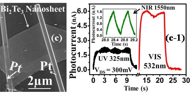
4 detect the light over a wide range covering from UV, NIR and telecommunication band (1550 nm) with high photoresponsivity. Results Nanosheets or flakes were deposited by using the scotch tape method and controlled FIB milling (ion beam current 50 pa and milling time < 5 Sec ) was performed on these nanosheets to obtain the nanowires of Bi 2Te 3 (Figure 1(a)). The energy dispersive X- ray spectroscopy (EDS) was done prior to the nanowire fabrication to know the elemental analysis and mapping of the deposited nanosheets. The inset in Figure 1(b) shows EDS spectrum detecting peaks of Bi and Te elements and atomic wt percentage was found about 39 and 61 respectively. The EDS mapping signal of Te (L ) and Bi (M ) is shown in the insets I and II of Figure 1(c) respectively. The HRTEM (high resolution transmission electron microscopy) characterization of nanosheets is shown in the experimental method section. The FIB based metal deposition gas injection system was used to make the Pt metal pads on the fabricated nanowires of Bi 2Te 3. The schematics used for optoeletronic characterization of the nanowire devices is shown in the Figure 1(d) where light was illuminated uniformly covering the whole device. The broadspectral photodetection was first studied in Bi 2Te 3 nanosheets and the false colour FESEM image of fabricated device with two platinum contacts is shown in the inset of Figure 2(a). The device was illuminated with UV, visible, NIR lights and time dependent rise or decrease in device s current was measured. The sharp sudden rise or decrease in current was observed when the incident light was either switched ON/OFF respectively. Different bias voltages were applied and the corresponding increase in photocurrent was measured which is shown in Fig. 2(a). The increase in current depends on the applied bias voltage through the relation, I g = 2I peµ(w/l)v sd where is mobility, e is the electronic charge, W is the width and L is the channel length of the device. With higher applied bias voltage, higher photocurrent was observed. The obtained data clearly shows that Bi 2Te 3 nanosheet exhibits broad spectral photosensitivity. The sensitivity towards 1550 nm light is very important since it is widely used in telecommunication applications. The rise and decay times were obtained by fitting the curves with 4
5 t t τ equations I = I 0 (1 eτr) and I = I 0 (e d ) respectively where τ r and τ d are the rise and the decay time constants respectively (supplementary information Figure S1). The τ r and τ d were observed in millisecond time scale for UV, visible and NIR lights illuminations (Table 1). The characteristic values obtained in the present study are comparable and/or better with results reported on topological insulator based nanowires or films. The curves shown in Fig. 2(a) clearly demonstrate the Bi 2Te 3 nanosheet shows broad spectral sensitivity and device was found stable at different bias voltages (25 mv 300 mv). The responsivity is a very essential and an important parameter for any kind of photodetector and can be estimated through the measured photocurrent, wavelength of light, device area and power density of the incident laser light. The Fig. 2(b) shows the responsivity curves of the nanosheet as a function of applied bias voltage. For UV, visible and NIR light irradiations, we observed linear increase in the responsivity values. The responsivity was found better for NIR light compared to visible and UV lights. The photocurrent and responsivity of the nanosheet device were further characterized as a function of laser power density (NIR 1550nm) and the curves are shown in the Figure 2(c). As expected, the decrease in responsivity was observed as a function of increase in the laser power density which is consistent with the other published results on topological insulators based nanowires 14, films 15. The curves represent that the nanosheets respond well to incoming light from UV to NIR region and this material could be the alternative choice for the present photodetectors either to replace silicon which do not have NIR sensitivity beyond ~ 1100 nm or InGaAs which do not show UV sensitivity. Three more nanosheets were tested further where we find similar broad spectral photoresponse and responsivity. The device images and photoconductivity measurements for these nanosheets are shown in the supplementary information Figure S2-S4. Photodetectors based on nanowires are often show ultrahigh performance properties compared to film or bulk counterparts. Earlier reports on fabricated nanowires of Bi 2Se 3 showed high performance properties but was not investigated for telecom wavelength 14. Bi 2Te 3 with bandgap ev 9 is more appealing material for NIR sensing applications and we fabricated nanowires by FIB milling method ( NW1 and 5
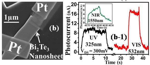
6 NW2 as shown in insets of Figure 3(a) and 3(d) respectively). The fabricated NW1 was first tested for UV and NIR light irradiations and time dependent changes in photocurrent due to light ON/OFF cycles were monitored at a constant bias voltage and at different laser power densities as shown in the Fig. 3(a). After each cycle, the power density was slightly increased and the corresponding rise in photocurrent was monitored. Thus the increase in the amplitude of photocurrents indicates corresponding increase in the power density of laser light illumination in mw/cm 2 as shown by the numbers. For every increase in the power density of the laser at a fixed bias voltage shows the increase in the photocurrent and higher photocurrent was observed for the 1550 nm. The periodic On/OFF cycles with different power densities and laser wavelengths represent the stability of the device working at the room temperature. The device was also exposed under visible laser radiations 532 nm and the bias voltage dependent photocurrent increase was monitored which is shown in the supplementary information Figure S5. The photocurrent values measured at 300 mv bias voltages were used to know the responsivity and detectivity curves for UV, visible and NIR wavelengths are shown in the Fig.3 (b). The higher responsivity was observed for the NIR light (1550 nm). The laser power dependent photocurrent measurements were further repeated at different bias voltages and corresponding curves for NIR light (1064 nm) illumination are shown in the Figure 3(c). The fabricated nanowires were found nicely detecting the incident light at different bias voltages and the linear increase in photocurrent was observed as a function of incident power density. The bias voltages were applied from mv and responsivity curve for the data at 300 mv is shown in the inset of Fig 3(c). At higher power density, generation of more electron hole pair is expected which contribute to the enhancement in photocurrent and the linear response suggest that traps or deformations present in the fabricated material do not affect the photoconductivity. The photoconductivity measurements were repeated for another fabricated Bi 2Te 3 nanowire device (NW2, inset Figure 3(d)). The time dependent photocurrent measurements were performed under UV, visible and NIR wavelengths and responsivity curves as a function of applied bias voltage are shown in Fig. 3(d). The time dependent photocurrent curves for UV, Visible wavelengths at different bias voltages are shown in 6
7 the Figure 3(e) and for NIR wavelength is shown in the supplementary information Figure S6. The sudden rise or drop in photocurrent measurement is due to switch ON or OFF cycles of the laser light exposure during the constant applied bias voltage. The reproducibility in broad spectral photodetection was clearly observed. Figure 3(f) represents the performance of NW2 device under the illumination of NIR laser 1550 nm at 300mV bias voltage. The maximum photoresponsivity about 778 A/W was observed at lower power density and the inset shows the detectivity of the NW2 device as a function of incident laser power density. The values of responsivity and detectivity at 300 mv bias voltage are shown in Table (1) which are quite competitive compared to other reported values. The reproducibility of broadspectral photoresponse was also observed in NW3 device and the data is shown in the supplementary information Figure S3. Topological insulators based materials possess intrinsic robust transport properties and expected that presence of nonmagnetic impurities and material deformations do not affect them. Here we used FIB fabrication process to test the robust photoconducting nature of Bi 2Te 3 nanosheet and nanowires because FIB milling technique inherently implants Ga ions and some deformation in nanosheet during fabrication of nanowires from the nanosheet. First we have studied photoresponse of deposited nanosheet contacted with Pt metal electrodes which is shown in the inset of Figure 4(a). The time dependent photocurrent measurements under the illumination of UV, Visible and NIR (Figure S7) lights were first carried out to confirm the broad spectral optoelectronic properties. In the second step nanosheet was transformed into a nanowire form Fab_NW-1 (inset of Figure 4(b)) and the similar to nanosheet, broad spectral photoconductivity measurements were repeated and shown in the Fig. 4(b). The fabricated nanowire clearly showed the broad spectral nature of photoresponse. The Fab_NW-1 wire was further narrowed in second step to get the Fab_NW-2 device ( inset Figure 4(c)) and the nature of broad spectral photoconductivity was clearly noticeable (curves in Fig. 4(c). In 3 rd step Fab_NW-2 device was further narrowed down to 160 nm where we expected more distortions and Ga implantations (device image in 7
8 inset Figure 4(d)). The time and applied bias voltage dependent photoconductivity measurements for this device are shown in the Fig. 4(d). Still the broadspectral photoresponse is clearly visible. The comparative bar chart of photoresponsivity observed at 300 mv bias voltage starting from the nanosheet to milled nanowire device Fab_NW-3, is shown in the Figure 4(e). The bars clearly represent that there is no degradation of the photocurrent even after the milling was performed 3 times. The slight rise in photocurrent for all wavelengths was observed. The better performance in photodetection could be due to the nano confinement effects and more electron hole pair generation for every effective incident photon. The reproducibility of robust nature photoconductivity under repetitive milling operations was also checked on other device and data is shown in the supplementary information Figure S3. The aging parameters such as the functioning of the device over a longer period, storage of nanowire device at ambient conditions are important to know the robustness of device. Important to note that nanowire based devices could be damaged due to moisture, exposure to ambient conditions and longer duration storage and hence device s performance may be degraded over the time. In Figure 4(f), we have tested the robustness of the device over 4 month s time. The curves in the figure show time dependent photocurrent measurements at constant bias 300 mv. The black curve shows the measurements done after the fabrication of the device within a day time whereas the green and pink curves represent the photoconductivity measurements performed after 35 and 120 days interval of time, respectively. The Figure S8 shows the changes in the gain values and a moderate degradation in device s performance was observed. Note that the device was stored at ambient conditions and some degradation is expected. Overall still it was convincingly showing the broadspectral photoresponse and photoresponsivity of about 210 A/W at 1550 nm was observed. Previously a very slow growth of oxide layer, ~ 2nm in 5700 hrs was observed in Bi 2Te 3 material under the continuous exposure of air 16. The oxidation of Bi 2Te 3 shifts the Fermi level towards up or down direction with respect to the Dirac point and this could be the reason behind slight degradation of photoconductivity in our devices. This indicates robust performance of the device and was not much affected by the ambient conditions. The detectivity and photoconductive gain 8
9 are important parameters for the imaging applications and can be estimated from the following relations D = (R A) (2eI d ) 1/2 and G = R hc λe respectively, where R is the responsivity, e is electronic charge, I d is dark current, A is the active area, h is Planck s constant, c is the velocity of light. The detectivity and photoconductive gain values are reported in the Table (1). Discussion: Nanoplates of Bi 2Te 3 represent a new class of tunable plasmonic material 10 and these devices can be further used to study the light matter interactions in various heterostructures. The previous reports on nanostructure based devices showed high performance optoelectronic properties due to quantum confinement effects 14,17,18. The Bi 2Te 3 nanowires fabricated and studied here show higher photoresponsivity ( ~ 778 A/W at 1550nm and 300 mv bias) which is better than the earlier reported responsivity ( 35 A/W at 532 nm) obtained from photodetectors based on graphene Bi 2Te 3 heterostructures 19 and MBE grown Bi 2Te 3 films 20. The higher values of the responsivity observed in our devices could be due to the strong light matter interactions, high quality of the deposited material, the large surface area to volume ratio favored by nano milling and the carrier transport through efficient surface states. This is because topological insulator based materials show transport properties through topological surface states (TSS) and bulk is insulating in nature, the efficient carrier transport property of TSS may be favourable to achieve the high performance photodetector. Note that the fabricated Bi 2Te 3 nanowire devices are better due to increase in surface to volume ratio, abundant surface carriers and compared to single layer dichalcogenides devices, absorption of light could be better since their thicknesses are large compared to single or bilayer devices. Taking into an account the short penetration length of the incident light, the top few layers of the material contribute more to the photocurrent generation hence in case of nanosheets or nanowires of TIs, more light absorption is favourable. 9
10 The significant and reproducible photocurrent was detected in all the devices studied here under periodic On/Off cycles of the laser light, the sudden rise and decay in photocurrent correspond to the On and Off state of the incident laser light. The saturation in photocurrent is clearly visible and the faster decay indicates that there are not so much charge trapping centers after the fabrication process got complete. Further, material inhomogentiy formed due to Ga implantation is not much affecting the photoresponse of the material when compared it with the bare nanosheet. The rise or decay times in sec or ms have been observed in many 2D material based systems and topological insulator based systems 21,22,23 19,24. Note that the rise or decay time constant values are estimated here either using the exponential rise or decay fit equations. However we find that rise time or decay time constant in ms are in good agreement (Table 1) with the published literature and show competitiveness for photodetector applications and the fast response indicate the efficient carrier transport facilitated may be due to the robust nature of the TSS and high mobility 25,26 which is far better as compared with the transition metal dichalcogenides 27,28. The broad spectral photodetection based on nanobelts, nanoribbons, nanosheets and emerging 2D materials have been recently published in a review article 29. The nanobelts of molybdenum trioxide 30, nanosheets of InSe ( = 850 nm) 31 and SnS 2 ( = 850 nm ) 32 show responsivity values 56 A/W, 2.975x10 3 and 1.22x10⁻⁸ A/W respectively (2,3,4). Other 2D materials like layered black phosphorus (BP) 33, BP/ 34 monolayer MoS 2, ferroelectric polymer film gated with ferroelectric material 34, graphene Bi 2Te 18 3, Bi 2Te 3-SnSe-Bi 2Te 35 3, Bi/WS 2/Si 36 and α-in 2Te 37 3 show responsivity values 0.4 x 10-3,3.54, 2570, 35, 5.5, 0.42 and 44 A/W, respectively (5,6,7,8,9,10,11). Compared to these materials, responsivity obtained with nanowires of Bi 2Te 3 is much more competitive taking into account of single material and no gate field effects. Robust photoconduction observed here indicate that efficient carrier transport through TSS is resistant to material deformations caused by ion milling and non magnetic Ga impurities. Bi 2Te 3 in combination with other material such as WS 2 and Si have been demonstrated the broad spectral photoresponsivity 21,38. The nanoflakes of Sb 2SeTe 2 and thin films of Sb 2Te 3 have also shown high performing visible 39 and near 10
11 infrared 24 photodetection recently. Huang et al observed that transport through TSS can tolerate the surface oxidation and molecules absorbed on the samples surface 40 and our previous work also showed the robustness of TSS towards the Ga ion milling and inherent material deformations 26,41. In Fig. 4(f) we observed that even at sequential milling operations, the photosensitivity do not degrade. Here we explain that the observed increase in photocurrent mostly coming from surface states by considering the milling of the device area i.e. changes in the nanowire widths corresponding to the change in the photocurrent. Figure 5 shows the energy dispersion diagram illustrating the various possibilities of optical excitation and photocurrent generation. The Fig. 5 shows that under illumination of light, hole electron pairs are generated due to the possibility in both bulk (I) as well as in TSS (III). Since the topological insulator materials show metallic surface states having Dirac cone distribution hence the light can be detected over a broad spectral range similar to that of graphene 5. On the other hand, the bulk band gap of Bi 2Te 3 is ~ ev 9 and absorption of light will eventually create the electron hole pairs. The total conductance is the combination of conductance coming from the surface states and contribution of bulk conductivity and can be written as G total = G Surface + G Bulk(WH/L), where W, H and L are width, height and length of the bulk channel. The defects, implanted Ga ion may help to form vacancies and antisite defects which could dope the film that may shift the Fermi level either to the conductance or valence band resulting the conductance dominated by the bulk channel at room temp. Note that topological insulators systems are predicated to be robust against any nonmagnetic impurities or deformations. Previously we have studied low temp transport studies and found quantum oscillations at low temp demonstrating the robust nature of TSS 26,41. The absorption of light and generations of electron hole pairs are more effective in few layers of Bi 2Te 3. The bulk Bi 2Te 3 material shows large mean free path length ~ 60 nm 42 that makes easy for the excited carriers to likely drifting towards the conducting surface state channel (step II) as shown in the Fig. 5. The femtosecond ultrafast spectroscopy and angle resolved photoemission spectroscopy revealed that optically excited carriers, accumulated in bulk conduction (metastable population) feeds a no equilibrium population of the surface states 43. Under bias 11
12 condition, these accumulated carriers contributed to the rise in the photocurrent. The fabrication approach indicates the narrowing of the sample i.e. contribution from the bulk channel is less but even though the photocurrent found increasing which suggests that contribution of bulk is less if we compare the nanosheet to Fab_NW-3 dimensions (inset Fig. 4(d)). The reason could be a stronger surface contribution to the conductance, increased surface to volume ratio, enhanced free carriers generation by quantum confinement effects etc. The optical absorption of TI based materials is strongly depends on thickness of the material and dramatic enhancement in the performance of the photodetector was theoretically seen when thickness of the material was reduced to several quintuple layers 5. Theoretically the optical conductivity of topological insulator Bi 2Se 3 thin films was seen over a broadspectral region spanning from infrared to visible 44. The different routes of optical absorption in thin films of TI were observed and transitions were mainly arising from intraband, interbands, and surface states in the valence band to surface states in conduction bands. Previously the MBE grown Bi 2Te 3 thin films on Si were used to detect photoresponses at NIR wavelengths and the responsivity was observed ~ 3. 64x 10-3 and 3. 32x 10-2 A/W for 1064 and 1550 nm wavelengths respectively 20. Here we have observed ultrahigh responsivity of ~ 778 A/W at NIR excitation with 1550 nm and the overall performance values of Bi 2Te 3 nanosheets and nanowires are shown in table 1, which are either better or competitive. This indicates that nanosheets or nanowires of Bi 2Te 3 material have potential technological use in photodetection without the need of high drain to source bias or gate voltages (Table 1). 12
13 Conclusion: The nanosheet and/or nanowires of Bi 2Te 3 show high performance optoelectronic properties. The clear broad spectral photodetection for UV, visible and NIR wavelengths was observed in all the measured samples. The robust nature of photoconductivity in Bi 2Te 3 against the nano milling conditions is evident. The devices stored at ambient conditions show slight degradation in optoelectronic properties while keeping the broad spectral response unaffected. The observed robust ultra-high photoresponsivity and broadband photodetection indicate exciting optoelectronic applications which can be exploited further as robust photodetectors are having potential applications in nanocircuits, nanodevices, photodetectors and sensors. Method: High resolution transmission electron microscopy (HRTEM, model: Tecnai G2F30 STWIN) was employed to characterize the specimens of Bi 2Te 3. In general, nano-sheets of Bi 2Te 3 normally with either elongated or flat morphologies were delineated throughout in the microstructure (Figures. 6(a) and (c)). The elongated small nanosheets appeared very tiny with the length and width of about 50 and 5 nm, respectively (Figure. 6(a)). A corresponding selected area electron diffraction pattern (SAED) from the bundles of elongated morphologies (Figure. 6(a)) exhibits a set of Debye rings (inset in Figure. 6(a)). The important planes of Bi 2Te 3 rhombohedral crystal structure (lattice constants: a = nm, = 24.13, space group: R3 m, reference: JCPDS card no ) with interplanar (d) spacings 0.32, 0.24 and 0.22 nm corresponding to hkl: 221, 433, and 110, are marled as 1, 2, and 3, respectively on the inset of Figure 6(a). A high resolution image of atomic planes from the encircled region in Figure. 6(a) further shows the atomic planes (Figure 6(b)) with the interlayer separation of about 0.32 nm corresponding to hkl indices of 221 of Bi 2Te 3 rhombohedral crystal. In another flat morphology of nano-sheets as depicted in Figure 6(c), 13
14 the overall area is larger with respect to elongated morphology (Figure. 6(a)). A corresponding atomic scale image recorded from the encircled area of Figure. 6(c) exhibits a set of atomic planes of d values of about 0.24 nm with hkl indices of 433 of Bi 2Te 3 rhombohedral crystal. References 1 Rauch, T. et al. Near-infrared imaging with quantum-dot-sensitized organic photodiodes. Nat. Photonics 3, , (2009). 2 Mueller, T., Xia, F. N. A. & Avouris, P. Graphene photodetectors for high-speed optical communications. Nat. Photonics 4, , (2010). 3 Furchi, M. et al. Microcavity-Integrated Graphene Photodetector. Nano Lett. 12, , (2012). 4 Lu, S. B. et al. Third order nonlinear optical property of Bi 2Se 3. Opt. Express 21, , (2013). 5 Zhang, X. A., Wang, J. & Zhang, S. C. Topological insulators for high-performance terahertz to infrared applications. Phy. Rev. B 82, (2010). 6 Lin, Y. H. et al. Using n- and p-type Bi 2Te 3 Topological Insulator Nanoparticles To Enable Controlled Femtosecond Mode-Locking of Fiber Lasers. Acs Photonics 2, , (2015). 7 Jiang, T. et al. Broadband High-Responsivity Photodetectors Based on Large-Scale Topological Crystalline Insulator SnTe Ultrathin Film Grown by Molecular Beam Epitaxy. Adv. Opt. Mater., 5, , (2016). 8 Saleemi, M., Toprak, M. S., Li, S. H., Johnsson, M. & Muhammed, M. Synthesis, processing, and thermoelectric properties of bulk nanostructured bismuth telluride (Bi 2Te 3). J. Mater. Chem. 22, , (2012). 9 Chen, Y. L. et al. Experimental Realization of a Three-Dimensional Topological Insulator, Bi 2Te 3. Science 325, , (2009). 10 Zhao, M. et al. Actively Tunable Visible Surface Plasmons in Bi 2Te 3 and their Energy-Harvesting Applications. Adv.Mater. 28, , (2016). 11 Yao, J. D., Shao, J. M., Li, S. W., Bao, D. H. & Yang, G. W. Polarization dependent photocurrent in the Bi 2Te 3 topological insulator film for multifunctional photodetection. Sci. Rep., 5, (2015). 12 Chen, S. Q. et al. Broadband optical and microwave nonlinear response in topological insulator. Opt. Mater. Express 4, , (2014). 13 Tang, P. H. et al. Topological Insulator: Bi 2Te 3 Saturable Absorber for the Passive Q-Switching Operation of an in-band Pumped 1645-nm Er:YAG Ceramic Laser. Ieee Photonics J. 5, (2013). 14 Sharma, A., Bhattacharyya, B., Srivastava, A. K., Senguttuvan, T. D. & Husale, S. High performance broadband photodetector using fabricated nanowires of bismuth selenide. Sci. Rep., 6, 19138, (2016). 15 Zhang, H. B., Zhang, X. J., Liu, C., Lee, S. T. & Jie, J. S. High-Responsivity, High-Detectivity, Ultrafast Topological Insulator Bi 2Se 3/Silicon Heterostructure Broadband Photodetectors. Acs Nano 10, , (2016). 14
15 16 Bando, H. et al. The time-dependent process of oxidation of the surface of Bi 2Te 3 studied by x- ray photoelectron spectroscopy. J. Phys-Condens Matt. 12, , (2000). 17 Hu, L. F., Yan, J., Liao, M. Y., Wu, L. M. & Fang, X. S. Ultrahigh External Quantum Efficiency from Thin SnO 2 Nanowire Ultraviolet Photodetectors. Small 7, , (2011). 18 Cao, L. Y. et al. Engineering light absorption in semiconductor nanowire devices. Nat.Mater. 8, , (2009). 19 Qiao, H. et al. Broadband Photodetectors Based on Graphene-Bi 2Te 3 Heterostructure. Acs Nano 9, , (2015). 20 Liu, J. J. et al. Bi 2Te 3 photoconductive detectors on Si. Appl. Phys. Lett. 110, (2017). 21 Yao, J. D., Shao, J. M., Wang, Y. X., Zhao, Z. R. & Yang, G. W. Ultra-broadband and high response of the Bi 2Te 3-Si heterojunction and its application as a photodetector at room temperature in harsh working environments. Nanoscale 7, , (2015). 22 Khan, M. F. et al. Photocurrent Response of MoS2 Field-Effect Transistor by Deep Ultraviolet Light in Atmospheric and N-2 Gas Environments. Acs Appl. Mater. Inter. 6, , (2014). 23 Perea-Lopez, N. et al. CVD-grown monolayered MoS 2 as an effective photosensor operating at low-voltage. 2D Mater. 1, , (2014). 24 Zheng, K. et al. Optoelectronic characteristics of a near infrared light photodetector based on a topological insulator Sb 2Te 3 film. J. Mater. Chem. C 3, , (2015). 25 He, L. et al. Surface-Dominated Conduction in a 6 nm thick Bi 2Se 3 Thin Film. Nano Lett. 12, , (2012). 26 Bhattacharyya, B., Sharma, A., Awana, V. P. S., Senguttuvan, T. D. & Husale, S. FIB synthesis of Bi 2Se 3 1D nanowires demonstrating the co-existence of Shubnikov-de Haas oscillations and linear magnetoresistance. J. Phys-Condens Matt., 29, 07LT01, (2017). 27 Kumar, R., Sharma, A., Kaur, M. & Husale, S. Pt-Nanostrip-Enabled Plasmonically Enhanced Broad Spectral Photodetection in Bilayer MoS 2. Adv. Opt. Mater., 5, (2017). 28 Yin, Z. Y. et al. Single-Layer MoS 2 Phototransistors. Acs Nano 6, 74-80, (2012). 29 Dhanabalan, S. C., Ponraj, J. S., Zhang, H. & Bao, Q. L. Present perspectives of broadband photodetectors based on nanobelts, nanoribbons, nanosheets and the emerging 2D materials. Nanoscale 8, , (2016). 30 Xiang, D., Han, C., Zhang, J. L. & Chen, W. Gap States Assisted MoO 3 Nanobelt Photodetector with Wide Spectrum Response. Sci. Rep., 4, (2014). 31 Feng, W. et al. Ultrahigh photo-responsivity and detectivity in multilayer InSe nanosheets phototransistors with broadband response. J. Mater. Chem. C 3, , (2015). 32 Tao, Y. R., Wu, X. C., Wang, W. & Wang, J. A. Flexible photodetector from ultraviolet to near infrared based on a SnS 2 nanosheet microsphere film. J. Mater. Chem. C 3, , (2015). 33 Deng, Y. X. et al. Black Phosphorus-Monolayer MoS 2 van der Waals Heterojunction p-n Diode. Acs Nano 8, , (2014). 34 Yuan, H. T. et al. Polarization-sensitive broadband photodetector using a black phosphorus vertical p-n junction. Nat. Nanotechno., 10, , (2015). 35 Yao, J. D., Zheng, Z. Q. & Yang, G. W. All-Layered 2D Optoelectronics: A High-Performance UVvis-NIR Broadband SnSe Photodetector with Bi 2Te 3 Topological Insulator Electrodes. Adv. Funct. Mater., 27, (2017). 36 Yao, J. D., Zheng, Z. Q. & Yang, G. W. Promoting the Performance of Layered-Material Photodetectors by Alloy Engineering. Acs Appl. Mater. Inter., 8, , (2016). 37 Yao, J. D., Deng, Z. X., Zheng, Z. Q. & Yang, G. W. Stable, Fast UV-Vis-NIR Photodetector with Excellent Responsivity, Detectivity, and Sensitivity Based on alpha-in 2Te 3 Films with a Direct Bandgap. Acs Appl. Mater. Inter., 8, , (2016). 15
16 38 Yao, J. D., Zheng, Z. Q., Shao, J. M. & Yang, G. W. Stable, highly-responsive and broadband photodetection based on large-area multilayered WS 2 films grown by pulsed-laser deposition. Nanoscale 7, , (2015). 39 Huang, S. M. et al. Extremely high-performance visible light photodetector in the Sb 2SeTe 2 nanoflake. Sci. Rep., 7, 45413, (2017). 40 Huang, S. M. et al. Observation of surface oxidation resistant Shubnikov-de Haas oscillations in Sb 2SeTe 2 topological insulator. J. Appl. Phys., 121, (2017). 41 Bhattacharyya, B. et al. Observation of quantum oscillations in FIB fabricated nanowires of topological insulator (Bi 2Se 3). J. Phys-Condens Matt., 29, (2017). 42 Mavrokefalos, A. et al. Thermoelectric and structural characterizations of individual electrodeposited bismuth telluride nanowires. J. Appl. Phys., 105, , (2009). 43 Sobota, J. A. et al. Ultrafast Optical Excitation of a Persistent Surface-State Population in the Topological Insulator Bi 2Se 3. Phys. Rev. Lett., 108, (2012). 44 Li, L. L., Xu, W. & Peeters, F. M. Optical conductivity of topological insulator thin films. J. Appl. Phys., 117, , (2015). 45 Zang, C. et al. Photoresponse properties of ultrathin Bi 2Se 3 nanosheets synthesized by hydrothermal intercalation and exfoliation route. Appl. Surf. Sci., 316, , (2014). 46 Yao, J. D., Shao, J. M. & Yang, G. W. Ultra-broadband and high-responsive photodetectors based on bismuth film at room temperature. Sci. Rep., 5, (2015). 47 Liu, C. et al. Topological insulator Bi 2Se 3 nanowire/si heterostructure photodetectors with ultrahigh responsivity and broadband response. J. Mater. Chem. C 4, , (2016). 48 Yao, J. D., Zheng, Z. Q. & Yang, G. W. Layered-material WS 2/topological insulator Bi 2Te 3 heterostructure photodetector with ultrahigh responsivity in the range from 370 to 1550 nm. J. Mater. Chem. C 4, , (2016). Acknowledgments A.S. acknowledges the SRF fellowship of Council of Scientific and Industrial Research, India. S.H. and A.S. acknowledge CSIR s Network project Aquarius for the financial support. We sincerely thank HOD DU 2, Dr. V N Ojha for his support and encouragement. Author contributions A.S. deposited and localized the nanosheets, performed metallization using sputtering system and carried out all the optoelectronic measurements. A.S analysed all the the data and fabricated the nanodevices with SH. A.K.S. performed and analysed the HRTEM data. T.D.S. provided FIB tools, operational support and materials. S.H. conceived and supervised the research and wrote the manuscript. 16
17 Additional information Reprints and permissions information is available online at Correspondence and requests for materials should be addressed to S.H. Competing financial interests The authors declare no competing financial interests. Corresponding Author * 17
 shows the FIB fabricated Bi2Te3 nanowire. Fig.")
18 Figures Figure 1. Nanosheet and nanowires of Bi2Te3. Inset I and II in Fig. (a) show the Bi2Te3 nanosheet deposited using scotch tape method and selective FIB milling of the nanosheet. The Fig. (a) shows the FIB fabricated Bi2Te3 nanowire. Fig. (b) shows the FESEM image of Bi2Te3 nanosheet used for elemental analysis and inset represents the EDS characterization of the selected portion of the nanosheet. The rectangle in Fig. (c) shows the area used for EDS elemental mapping for Bi and Te as shown in inset I and II respectively. Fig. (d) represents the schematics used for the optoelectronics characterization. 18
 shows the bias voltage dependent responsivity curves measured under different light irradiations. Fig. (c) represents the NIR (1550 nm) laser power density dependent photocurrent and responsivity curves.")
19 Figure 2 Optoelectronic characterizations of as deposited Bi2Te3 nanosheet. Time dependent photocurrent measurements at different bias voltages and incident wavelengths (Fig. (a)). Inset is the false colour FESEM image of the Bi2Te3 nanosheet device. Fig. (b) shows the bias voltage dependent responsivity curves measured under different light irradiations. Fig. (c) represents the NIR (1550 nm) laser power density dependent photocurrent and responsivity curves. Inset in Fig. (c) shows the laser power density dependent detectivity curve. 19
 represents the Bi2Te3 nanowire device (NW1) used for time and incident power dependent photocurrent measurements under UV and NIR light illuminations.")
20 Figure 3. Optoelectronic characterization of FIB fabricated Bi2Te3 nanowires. Inset in Fig. (a) represents the Bi2Te3 nanowire device (NW1) used for time and incident power dependent photocurrent measurements under UV and NIR light illuminations. The responsivity and detectivity curves obtained for UV, visible and NIR lights are shown in Fig. (b). The photocurrent dependence on incident power density (Fig. (c)) at different bias voltages and inset shows the responsivity curve. Fig. (d f) represent the optoelectronic characterization for NW2 device (inset Fig. (d)). Fig. (d) shows the bias voltage dependent reponsivity curves observed for different wavelengths. The photocurrent measurement as a function of time in presence of visible and UV light illuminations at different bias voltages is shown in Fig. (e). Fig. 3(f) shows NIR laser power density dependent photocurrent and responsivity curves. Inset represents the power density dependent detectivity curve. 20
), Fab_NW1 (Fig. (b)), Fab_NW2 (Fig. (c)) and Fab_NW3 (Fig. (d)). Device images are shown in the insets of the respective graphs. Fig.")
21 Figure 4. Robustness and enhancements in photoconduction measurements. Time, applied bias and illumination light dependent photocurrent measurements for as deposited nanosheet (Fig. (a)), Fab_NW1 (Fig. (b)), Fab_NW2 (Fig. (c)) and Fab_NW3 (Fig. (d)). Device images are shown in the insets of the respective graphs. Fig. (e) represents the photocurrent comparison between nanosheet and fabricated nanodevices. Fig. (f) represents photocurrent response curves measured after ambient storage conditions as shown in the graph. 21
22 Figure 5 Schematic representation of energy band diagram illustrating the various possibilities of optical excitation and photocurrent generation 22
 bright field micrograph of elongated morphology (tiny nanosheets), (b) corresponding atomic scale image, (c)")
23 Figure 6. HRTEM results showing, (a) bright field micrograph of elongated morphology (tiny nanosheets), (b) corresponding atomic scale image, (c) bright field micrograph of another large nanosheet, (d) corresponding atomic scale image. Inset in (a) an electron diffraction pattern. 23
24 Table 1. Material λ R (AW -1 ) D (Jones) Gain/EQE Rise/Decay (nm) τr / τd, (s) Bi2Se nanosheets x / Sb2Te3 film x / Bi film x /1.9 Bi2Te3 film / Si x / Bi2Te x10-3 / Graphene x Bi2Se3 nanowire (NW) x /0.400 Bi2Se3 (NW)/ Si x x 10-6 / 5.5 x 10⁻⁶ Polycrystalline x /0.1 Bi2Te3 / Si 21 WS2 -Bi2Te x / ± x ± / 1.6 Bi2Te3 Flake ± x ± / ± x ± /0.44 Bi2Te3 NW (This work) ± x ± / ± x ± / ± x ± /
25 Table (1). Topological insulator material based photodetectors and performance comparison with our results. 25
26 Robust broad spectral photodetection (UV-NIR) and ultra high responsivity investigated in nanosheets and nanowires of Bi 2 Te 3 under harsh nano-milling conditions Alka Sharma 1,2, A. K. Srivastava 1,2, T. D. Senguttuvan 1,2 and Sudhir Husale 1,2 * 1 Academy of Scientific and Innovative Research (AcSIR), National Physical Laboratory, Council of Scientific and Industrial Research, Dr. K. S Krishnan Road, New Delhi , India. 2 National Physical Laboratory, Council of Scientific and Industrial Research, Dr. K. S Krishnan Road, New Delhi , India. * husalesc@nplindia.org Supplementary Information contents: 1. Rise and Decay time fit 2. Optoelectronic characterization of Bi 2 Te 3 nanosheets 3. Optoelectronic properties of Bi 2 Te 3 nanowires (NW) 4. Robustness and enhancements in photoconduction measurements 5. Photoconductivity of (visible) of NW1 device 6. Photoconductivity of (NIR) of NW2 device 7. Photoconductivity of (NIR) of Fab_NW1, Fab_NW2 and Fab_NW3 devices 8. Photoconducting gain of the device (Fab_NW3) 26
 curve fitting.")
27 1. Rise and Decay time fit and decay (green) curve fitting. Figure S1: Rise ( red ) 27

28 2. Optoelectronic characterization of Bi2Te3 nanosheets 28

29 Figure S2: Photoconductivity measurements on three more nanosheet devices 3. Optoelectronic characterization of Bi2Te3 nanowire Figure S3: Photoconductivity measurements on one more fabricated nanowire device 29


30 4. Robustness and enhancements in photoconduction measurements Figure S4: Photoconductivity measurements investigating robustness under harsh nano milling conditions 30

31 5. Photoconductivity of (visible) of NW1 device Figure S5: Bias voltage dependent photoconductivity measurements under illumination of visible light and device is NW1. 31

32 6. Photoconductivity of (NIR) of NW2 device Figure S6: Bias voltage dependent photoconductivity measurements under illumination of NIR light and device is NW2. 32

33 7. Photoconductivity of (NIR) of Fab_NW1, Fab_NW2 and Fab_NW3 devices Figure S7: Bias voltage dependent photoconductivity measurements under illumination of NIR light and devices are Fab_ NW1, Fab_ NW2 and Fab_ NW3. 33

34 8. Photoconducting gain of the device (Fab_NW3) Photoconductive gain of the device Fab_NW3. Figure S8: 34
Lecture 18: Photodetectors
 Lecture 18: Photodetectors Contents 1 Introduction 1 2 Photodetector principle 2 3 Photoconductor 4 4 Photodiodes 6 4.1 Heterojunction photodiode.................... 8 4.2 Metal-semiconductor photodiode................
Supporting Information
 Supporting Information High-Performance MoS 2 /CuO Nanosheet-on-1D Heterojunction Photodetectors Doo-Seung Um, Youngsu Lee, Seongdong Lim, Seungyoung Park, Hochan Lee, and Hyunhyub Ko * School of Energy
Esaki diodes in van der Waals heterojunctions with broken-gap energy band alignment
 Supplementary information for Esaki diodes in van der Waals heterojunctions with broken-gap energy band alignment Rusen Yan 1,2*, Sara Fathipour 2, Yimo Han 4, Bo Song 1,2, Shudong Xiao 1, Mingda Li 1,
LEDs, Photodetectors and Solar Cells
 LEDs, Photodetectors and Solar Cells Chapter 7 (Parker) ELEC 424 John Peeples Why the Interest in Photons? Answer: Momentum and Radiation High electrical current density destroys minute polysilicon and
Supplementary Information
 Supplementary Information For Nearly Lattice Matched All Wurtzite CdSe/ZnTe Type II Core-Shell Nanowires with Epitaxial Interfaces for Photovoltaics Kai Wang, Satish C. Rai,Jason Marmon, Jiajun Chen, Kun
InP-based Waveguide Photodetector with Integrated Photon Multiplication
 InP-based Waveguide Photodetector with Integrated Photon Multiplication D.Pasquariello,J.Piprek,D.Lasaosa,andJ.E.Bowers Electrical and Computer Engineering Department University of California, Santa Barbara,
SUPPLEMENTARY INFORMATION
 SUPPLEMENTARY INFORMATION Supplementary Information Real-space imaging of transient carrier dynamics by nanoscale pump-probe microscopy Yasuhiko Terada, Shoji Yoshida, Osamu Takeuchi, and Hidemi Shigekawa*
Supplementary Information
 DOI: 1.138/NPHOTON.212.19 Supplementary Information Enhanced power conversion efficiency in polymer solar cells using an inverted device structure Zhicai He, Chengmei Zhong, Shijian Su, Miao Xu, Hongbin
Luminous Equivalent of Radiation
 Intensity vs λ Luminous Equivalent of Radiation When the spectral power (p(λ) for GaP-ZnO diode has a peak at 0.69µm) is combined with the eye-sensitivity curve a peak response at 0.65µm is obtained with
SUPPLEMENTARY INFORMATION
 In the format provided by the authors and unedited. Photon-triggered nanowire transistors Jungkil Kim, Hoo-Cheol Lee, Kyoung-Ho Kim, Min-Soo Hwang, Jin-Sung Park, Jung Min Lee, Jae-Pil So, Jae-Hyuck Choi,
High Performance Visible-Blind Ultraviolet Photodetector Based on
 Supplementary Information High Performance Visible-Blind Ultraviolet Photodetector Based on IGZO TFT Coupled with p-n Heterojunction Jingjing Yu a,b, Kashif Javaid b,c, Lingyan Liang b,*, Weihua Wu a,b,
InP-based Waveguide Photodetector with Integrated Photon Multiplication
 InP-based Waveguide Photodetector with Integrated Photon Multiplication D.Pasquariello,J.Piprek,D.Lasaosa,andJ.E.Bowers Electrical and Computer Engineering Department University of California, Santa Barbara,
Selective improvement of NO 2 gas sensing behavior in. SnO 2 nanowires by ion-beam irradiation. Supporting Information.
 Supporting Information Selective improvement of NO 2 gas sensing behavior in SnO 2 nanowires by ion-beam irradiation Yong Jung Kwon 1, Sung Yong Kang 1, Ping Wu 2, *, Yuan Peng 2, Sang Sub Kim 3, *, Hyoun
High-Speed Scalable Silicon-MoS 2 P-N Heterojunction Photodetectors
 High-Speed Scalable Silicon-MoS 2 P-N Heterojunction Photodetectors Veerendra Dhyani 1, and Samaresh Das 1* 1 Centre for Applied Research in Electronics, Indian Institute of Technology Delhi, New Delhi-110016,
Introduction Fundamentals of laser Types of lasers Semiconductor lasers
 ECE 5368 Introduction Fundamentals of laser Types of lasers Semiconductor lasers Introduction Fundamentals of laser Types of lasers Semiconductor lasers How many types of lasers? Many many depending on
Physics of Waveguide Photodetectors with Integrated Amplification
 Physics of Waveguide Photodetectors with Integrated Amplification J. Piprek, D. Lasaosa, D. Pasquariello, and J. E. Bowers Electrical and Computer Engineering Department University of California, Santa
Supplementary Figure 1 Schematic illustration of fabrication procedure of MoS2/h- BN/graphene heterostructures. a, c d Supplementary Figure 2
 Supplementary Figure 1 Schematic illustration of fabrication procedure of MoS 2 /hon a 300- BN/graphene heterostructures. a, CVD-grown b, Graphene was patterned into graphene strips by oxygen monolayer
Nanophotonics: Single-nanowire electrically driven lasers
 Nanophotonics: Single-nanowire electrically driven lasers Ivan Stepanov June 19, 2010 Single crystaline nanowires have unique optic and electronic properties and their potential use in novel photonic and
OPTI510R: Photonics. Khanh Kieu College of Optical Sciences, University of Arizona Meinel building R.626
 OPTI510R: Photonics Khanh Kieu College of Optical Sciences, University of Arizona kkieu@optics.arizona.edu Meinel building R.626 Photodetectors Introduction Most important characteristics Photodetector
Functional Materials. Optoelectronic devices
 Functional Materials Lecture 2: Optoelectronic materials and devices (inorganic). Photonic materials Optoelectronic devices Light-emitting diode (LED) displays Photodiode and Solar cell Photoconductive
Optodevice Data Book ODE I. Rev.9 Mar Opnext Japan, Inc.
 Optodevice Data Book ODE-408-001I Rev.9 Mar. 2003 Opnext Japan, Inc. Section 1 Operating Principles 1.1 Operating Principles of Laser Diodes (LDs) and Infrared Emitting Diodes (IREDs) 1.1.1 Emitting Principles
Solar-energy conversion and light emission in an atomic monolayer p n diode
 Solar-energy conversion and light emission in an atomic monolayer p n diode Andreas Pospischil, Marco M. Furchi, and Thomas Mueller 1. I-V characteristic of WSe 2 p-n junction diode in the dark The Shockley
OPTOELECTRONIC and PHOTOVOLTAIC DEVICES
 OPTOELECTRONIC and PHOTOVOLTAIC DEVICES Outline 1. Introduction to the (semiconductor) physics: energy bands, charge carriers, semiconductors, p-n junction, materials, etc. 2. Light emitting diodes Light
Resonant Tunneling Device. Kalpesh Raval
 Resonant Tunneling Device Kalpesh Raval Outline Diode basics History of Tunnel diode RTD Characteristics & Operation Tunneling Requirements Various Heterostructures Fabrication Technique Challenges Application
Dynamics of Charge Carriers in Silicon Nanowire Photoconductors Revealed by Photo Hall. Effect Measurements. (Supporting Information)
") Dynamics of Charge Carriers in Silicon Nanowire Photoconductors Revealed by Photo Hall Effect Measurements (Supporting Information) Kaixiang Chen 1, Xiaolong Zhao 2, Abdelmadjid Mesli 3, Yongning He 2*
Dynamics of Charge Carriers in Silicon Nanowire Photoconductors Revealed by Photo Hall Effect Measurements (Supporting Information) Kaixiang Chen 1, Xiaolong Zhao 2, Abdelmadjid Mesli 3, Yongning He 2*
CONTENTS. 2.2 Schrodinger's Wave Equation 31. PART I Semiconductor Material Properties. 2.3 Applications of Schrodinger's Wave Equation 34
 CONTENTS Preface x Prologue Semiconductors and the Integrated Circuit xvii PART I Semiconductor Material Properties CHAPTER 1 The Crystal Structure of Solids 1 1.0 Preview 1 1.1 Semiconductor Materials
Silicon-based broadband antenna for high responsivity and polarization-insensitive photodetection at telecommunication wavelengths
 Received g 3 Accepted Jan 4 Published Feb 4 licon-based broadband antenna for high responsivity and polarization-insensitive photodetection at telecommunication wavelengths Keng-Te Lin, Hsuen-Li Chen,
Robert G. Hunsperger. Integrated Optics. Theory and Technology. Sixth Edition. 4ü Spri rineer g<
 Robert G. Hunsperger Integrated Optics Theory and Technology Sixth Edition 4ü Spri rineer g< 1 Introduction 1 1.1 Advantages of Integrated Optics 2 1.1.1 Comparison of Optical Fibers with Other Interconnectors
Performance and Loss Analyses of High-Efficiency CBD-ZnS/Cu(In 1-x Ga x )Se 2 Thin-Film Solar Cells
Se 2 Thin-Film Solar Cells") Performance and Loss Analyses of High-Efficiency CBD-ZnS/Cu(In 1-x Ga x )Se 2 Thin-Film Solar Cells Alexei Pudov 1, James Sites 1, Tokio Nakada 2 1 Department of Physics, Colorado State University, Fort
Performance and Loss Analyses of High-Efficiency CBD-ZnS/Cu(In 1-x Ga x )Se 2 Thin-Film Solar Cells Alexei Pudov 1, James Sites 1, Tokio Nakada 2 1 Department of Physics, Colorado State University, Fort
SUPPLEMENTARY INFORMATION
 DOI: 1.138/NPHOTON.212.11 Supplementary information Avalanche amplification of a single exciton in a semiconductor nanowire Gabriele Bulgarini, 1, Michael E. Reimer, 1, Moïra Hocevar, 1 Erik P.A.M. Bakkers,
Supplementary Figure 1 High-resolution transmission electron micrograph of the
 Supplementary Figure 1 High-resolution transmission electron micrograph of the LAO/STO structure. LAO/STO interface indicated by the dotted line was atomically sharp and dislocation-free. Supplementary
Analog Synaptic Behavior of a Silicon Nitride Memristor
 Supporting Information Analog Synaptic Behavior of a Silicon Nitride Memristor Sungjun Kim, *, Hyungjin Kim, Sungmin Hwang, Min-Hwi Kim, Yao-Feng Chang,, and Byung-Gook Park *, Inter-university Semiconductor
Supporting Information. Vertical Graphene-Base Hot-Electron Transistor
 Supporting Information Vertical Graphene-Base Hot-Electron Transistor Caifu Zeng, Emil B. Song, Minsheng Wang, Sejoon Lee, Carlos M. Torres Jr., Jianshi Tang, Bruce H. Weiller, and Kang L. Wang Department
Quantum Condensed Matter Physics Lecture 16
 Quantum Condensed Matter Physics Lecture 16 David Ritchie QCMP Lent/Easter 2018 http://www.sp.phy.cam.ac.uk/drp2/home 16.1 Quantum Condensed Matter Physics 1. Classical and Semi-classical models for electrons
Frequency Tunable Low-Cost Microwave Absorber for EMI/EMC Application
 Progress In Electromagnetics Research Letters, Vol. 74, 47 52, 2018 Frequency Tunable Low-Cost Microwave Absorber for EMI/EMC Application Gobinda Sen * and Santanu Das Abstract A frequency tunable multi-layer
Photodiode: LECTURE-5
 LECTURE-5 Photodiode: Photodiode consists of an intrinsic semiconductor sandwiched between two heavily doped p-type and n-type semiconductors as shown in Fig. 3.2.2. Sufficient reverse voltage is applied
Contents. Nano-2. Nano-2. Nanoscience II: Nanowires. 2. Growth of nanowires. 1. Nanowire concepts Nano-2. Nano-2
 Contents Nanoscience II: Nanowires Kai Nordlund 17.11.2010 Faculty of Science Department of Physics Division of Materials Physics 1. Introduction: nanowire concepts 2. Growth of nanowires 1. Spontaneous
Atomristor: Non-Volatile Resistance Switching in Atomic Sheets of
 Atomristor: Non-Volatile Resistance Switching in Atomic Sheets of Transition Metal Dichalcogenides Ruijing Ge 1, Xiaohan Wu 1, Myungsoo Kim 1, Jianping Shi 2, Sushant Sonde 3,4, Li Tao 5,1, Yanfeng Zhang
Semiconductor Physics and Devices
 Metal-Semiconductor and Semiconductor Heterojunctions The Metal-Oxide-Semiconductor Field-Effect Transistor (MOSFET) is one of two major types of transistors. The MOSFET is used in digital circuit, because
photolithographic techniques (1). Molybdenum electrodes (50 nm thick) are deposited by
. Molybdenum electrodes (50 nm thick) are deposited by") Supporting online material Materials and Methods Single-walled carbon nanotube (SWNT) devices are fabricated using standard photolithographic techniques (1). Molybdenum electrodes (50 nm thick) are deposited
Supporting online material Materials and Methods Single-walled carbon nanotube (SWNT) devices are fabricated using standard photolithographic techniques (1). Molybdenum electrodes (50 nm thick) are deposited
Chapter 3 OPTICAL SOURCES AND DETECTORS
 Chapter 3 OPTICAL SOURCES AND DETECTORS 3. Optical sources and Detectors 3.1 Introduction: The success of light wave communications and optical fiber sensors is due to the result of two technological breakthroughs.
Basic concepts. Optical Sources (b) Optical Sources (a) Requirements for light sources (b) Requirements for light sources (a)
 Optical Sources (a) Requirements for light sources (b) Requirements for light sources (a)") Optical Sources (a) Optical Sources (b) The main light sources used with fibre optic systems are: Light-emitting diodes (LEDs) Semiconductor lasers (diode lasers) Fibre laser and other compact solid-state
Optical Sources (a) Optical Sources (b) The main light sources used with fibre optic systems are: Light-emitting diodes (LEDs) Semiconductor lasers (diode lasers) Fibre laser and other compact solid-state
Photoconduction studies on GaN nanowire transistors under UV and polarized UV illumination
 Chemical Physics Letters 389 (24) 176 18 www.elsevier.com/locate/cplett Photoconduction studies on GaN nanowire transistors under UV and polarized UV illumination Song Han, Wu Jin, Daihua Zhang, Tao Tang,
SUPPLEMENTARY INFORMATION
 SUPPLEMENTARY INFORMATION doi: 1.138/nphoton.211.25 Efficient Photovoltage Multiplication in Carbon Nanotubes Leijing Yang 1,2,3+, Sheng Wang 1,2+, Qingsheng Zeng, 1,2, Zhiyong Zhang 1,2, Tian Pei 1,2,
Impact of the light coupling on the sensing properties of photonic crystal cavity modes Kumar Saurav* a,b, Nicolas Le Thomas a,b,
 Impact of the light coupling on the sensing properties of photonic crystal cavity modes Kumar Saurav* a,b, Nicolas Le Thomas a,b, a Photonics Research Group, Ghent University-imec, Technologiepark-Zwijnaarde
Electronic devices-i. Difference between conductors, insulators and semiconductors
 Electronic devices-i Semiconductor Devices is one of the important and easy units in class XII CBSE Physics syllabus. It is easy to understand and learn. Generally the questions asked are simple. The unit
High-speed Ge photodetector monolithically integrated with large cross silicon-on-insulator waveguide
 [ APPLIED PHYSICS LETTERS ] High-speed Ge photodetector monolithically integrated with large cross silicon-on-insulator waveguide Dazeng Feng, Shirong Liao, Roshanak Shafiiha. etc Contents 1. Introduction
Vertical Nanowall Array Covered Silicon Solar Cells
 International Conference on Solid-State and Integrated Circuit (ICSIC ) IPCSIT vol. () () IACSIT Press, Singapore Vertical Nanowall Array Covered Silicon Solar Cells J. Wang, N. Singh, G. Q. Lo, and D.
Room-Temperature Si-Compatible Red Light Emission from In 2 Se 3 -Decorated Silicon Nanowires
 Nanoscience and Nanometrology 2017; 3(2): 46-50 http://www.sciencepublishinggroup.com/j/nsnm doi: 10.11648/j.nsnm.20170302.12 ISSN: 2472-3622 (Print); ISSN: 2472-3630 (Online) Communication Room-Temperature
Design and Simulation of N-Substrate Reverse Type Ingaasp/Inp Avalanche Photodiode
 International Refereed Journal of Engineering and Science (IRJES) ISSN (Online) 2319-183X, (Print) 2319-1821 Volume 2, Issue 8 (August 2013), PP.34-39 Design and Simulation of N-Substrate Reverse Type
ECE 340 Lecture 29 : LEDs and Lasers Class Outline:
 ECE 340 Lecture 29 : LEDs and Lasers Class Outline: Light Emitting Diodes Lasers Semiconductor Lasers Things you should know when you leave Key Questions What is an LED and how does it work? How does a
Simulation of High Resistivity (CMOS) Pixels
 Pixels") Simulation of High Resistivity (CMOS) Pixels Stefan Lauxtermann, Kadri Vural Sensor Creations Inc. AIDA-2020 CMOS Simulation Workshop May 13 th 2016 OUTLINE 1. Definition of High Resistivity Pixel Also
Simulation of High Resistivity (CMOS) Pixels Stefan Lauxtermann, Kadri Vural Sensor Creations Inc. AIDA-2020 CMOS Simulation Workshop May 13 th 2016 OUTLINE 1. Definition of High Resistivity Pixel Also
Fabrication of antenna integrated UTC-PDs as THz sources
 Invited paper Fabrication of antenna integrated UTC-PDs as THz sources Siwei Sun 1, Tengyun Wang, Xiao xie 1, Lichen Zhang 1, Yuan Yao and Song Liang 1* 1 Key Laboratory of Semiconductor Materials Science,
Key Questions. What is an LED and how does it work? How does a laser work? How does a semiconductor laser work? ECE 340 Lecture 29 : LEDs and Lasers
 Things you should know when you leave Key Questions ECE 340 Lecture 29 : LEDs and Class Outline: What is an LED and how does it How does a laser How does a semiconductor laser How do light emitting diodes
Photonic Crystal Slot Waveguide Spectrometer for Detection of Methane
 Photonic Crystal Slot Waveguide Spectrometer for Detection of Methane Swapnajit Chakravarty 1, Wei-Cheng Lai 2, Xiaolong (Alan) Wang 1, Che-Yun Lin 2, Ray T. Chen 1,2 1 Omega Optics, 10306 Sausalito Drive,
Hierarchical CoNiSe2 nano-architecture as a highperformance electrocatalyst for water splitting
 Nano Res. Electronic Supplementary Material Hierarchical CoNiSe2 nano-architecture as a highperformance electrocatalyst for water splitting Tao Chen and Yiwei Tan ( ) State Key Laboratory of Materials-Oriented
Index. BaF 2 crystal 41 biochemical sensor 7, 316, ,
 Index acousto-optic effect 243 44 air bandedge 35, 266 air gap 188, 197, 224, 240 41 air holes 16 17, 52 53, 55, 64, 189, 192, 216 18, 241 43, 245, 266 68, 270 72, 298 99, 333 34, 336 37, 341 42 air pores
Department of Electrical Engineering IIT Madras
 Department of Electrical Engineering IIT Madras Sample Questions on Semiconductor Devices EE3 applicants who are interested to pursue their research in microelectronics devices area (fabrication and/or
Optical Fiber Communication Lecture 11 Detectors
 Optical Fiber Communication Lecture 11 Detectors Warriors of the Net Detector Technologies MSM (Metal Semiconductor Metal) PIN Layer Structure Semiinsulating GaAs Contact InGaAsP p 5x10 18 Absorption InGaAs
HIGH-EFFICIENCY MQW ELECTROABSORPTION MODULATORS
 HIGH-EFFICIENCY MQW ELECTROABSORPTION MODULATORS J. Piprek, Y.-J. Chiu, S.-Z. Zhang (1), J. E. Bowers, C. Prott (2), and H. Hillmer (2) University of California, ECE Department, Santa Barbara, CA 93106
Optical Receivers Theory and Operation
 Optical Receivers Theory and Operation Photo Detectors Optical receivers convert optical signal (light) to electrical signal (current/voltage) Hence referred O/E Converter Photodetector is the fundamental
10/14/2009. Semiconductor basics pn junction Solar cell operation Design of silicon solar cell
 PHOTOVOLTAICS Fundamentals PV FUNDAMENTALS Semiconductor basics pn junction Solar cell operation Design of silicon solar cell SEMICONDUCTOR BASICS Allowed energy bands Valence and conduction band Fermi
Investigation of the tapered waveguide structures for terahertz quantum cascade lasers
 Invited Paper Investigation of the tapered waveguide structures for terahertz quantum cascade lasers T. H. Xu, and J. C. Cao * Key Laboratory of Terahertz Solid-State Technology, Shanghai Institute of
Introduction to Optoelectronic Devices
 Introduction to Optoelectronic Devices Dr. Jing Bai Assistant Professor Department of Electrical and Computer Engineering University of Minnesota Duluth October 30th, 2012 1 Outline What is the optoelectronics?
Nanowires for Quantum Optics
 Nanowires for Quantum Optics N. Akopian 1, E. Bakkers 1, J.C. Harmand 2, R. Heeres 1, M. v Kouwen 1, G. Patriarche 2, M. E. Reimer 1, M. v Weert 1, L. Kouwenhoven 1, V. Zwiller 1 1 Quantum Transport, Kavli
Han Liu, Adam T. Neal, Yuchen Du and Peide D. Ye
 Fundamentals in MoS2 Transistors: Dielectric, Scaling and Metal Contacts Han Liu, Adam T. Neal, Yuchen Du and Peide D. Ye Department of Electrical and Computer Engineering and Birck Nanotechnology Center,
Chapter 1. Introduction
 Chapter 1 Introduction 1.1 Introduction of Device Technology Digital wireless communication system has become more and more popular in recent years due to its capability for both voice and data communication.
Nd:YSO resonator array Transmission spectrum (a. u.) Supplementary Figure 1. An array of nano-beam resonators fabricated in Nd:YSO.
 Supplementary Figure 1. An array of nano-beam resonators fabricated in Nd:YSO.") a Nd:YSO resonator array µm Transmission spectrum (a. u.) b 4 F3/2-4I9/2 25 2 5 5 875 88 λ(nm) 885 Supplementary Figure. An array of nano-beam resonators fabricated in Nd:YSO. (a) Scanning electron microscope
a Nd:YSO resonator array µm Transmission spectrum (a. u.) b 4 F3/2-4I9/2 25 2 5 5 875 88 λ(nm) 885 Supplementary Figure. An array of nano-beam resonators fabricated in Nd:YSO. (a) Scanning electron microscope
Novel laser power sensor improves process control
 Novel laser power sensor improves process control A dramatic technological advancement from Coherent has yielded a completely new type of fast response power detector. The high response speed is particularly
SUPPLEMENTARY INFORMATION
 Electronic Supplementary Material (ESI) for Nanoscale. This journal is The Royal Society of Chemistry 2015 SUPPLEMENTARY INFORMATION Diameter-dependent thermoelectric figure of merit in single-crystalline
MoS 2 nanosheet phototransistors with thicknessmodulated
 Supporting Information MoS 2 nanosheet phototransistors with thicknessmodulated optical energy gap Hee Sung Lee, Sung-Wook Min, Youn-Gyung Chang, Park Min Kyu, Taewook Nam, # Hyungjun Kim, # Jae Hoon Kim,
Fabrication of High-Speed Resonant Cavity Enhanced Schottky Photodiodes
 Fabrication of High-Speed Resonant Cavity Enhanced Schottky Photodiodes Abstract We report the fabrication and testing of a GaAs-based high-speed resonant cavity enhanced (RCE) Schottky photodiode. The
CMOS Phototransistors for Deep Penetrating Light
 CMOS Phototransistors for Deep Penetrating Light P. Kostov, W. Gaberl, H. Zimmermann Institute of Electrodynamics, Microwave and Circuit Engineering, Vienna University of Technology Gusshausstr. 25/354,
Coherent Receivers Principles Downconversion
 Coherent Receivers Principles Downconversion Heterodyne receivers mix signals of different frequency; if two such signals are added together, they beat against each other. The resulting signal contains
A silicon avalanche photodetector fabricated with standard CMOS technology with over 1 THz gain-bandwidth product
 A silicon avalanche photodetector fabricated with standard CMOS technology with over 1 THz gain-bandwidth product Myung-Jae Lee and Woo-Young Choi* Department of Electrical and Electronic Engineering,
SILICON NANOWIRE HYBRID PHOTOVOLTAICS
 SILICON NANOWIRE HYBRID PHOTOVOLTAICS Erik C. Garnett, Craig Peters, Mark Brongersma, Yi Cui and Mike McGehee Stanford Univeristy, Department of Materials Science, Stanford, CA, USA ABSTRACT Silicon nanowire
Design, Fabrication, Characterization, and Application of Semiconductor Nanocomposites
 Design, Fabrication, Characterization, and Application of Semiconductor Nanocomposites Yang-Fang Chen Department of Physics, National Taiwan University, Taipei, Taiwan 1 I. A perfect integration of zero
Vertically Aligned BaTiO 3 Nanowire Arrays for Energy Harvesting
 Electronic Supplementary Material (ESI) for Electronic Supplementary Information (ESI) Vertically Aligned BaTiO 3 Nanowire Arrays for Energy Harvesting Aneesh Koka, a Zhi Zhou b and Henry A. Sodano* a,b
Applications of Steady-state Multichannel Spectroscopy in the Visible and NIR Spectral Region
 Feature Article JY Division I nformation Optical Spectroscopy Applications of Steady-state Multichannel Spectroscopy in the Visible and NIR Spectral Region Raymond Pini, Salvatore Atzeni Abstract Multichannel
Arūnas Krotkus Center for Physical Sciences & Technology, Vilnius, Lithuania
 Arūnas Krotkus Center for Physical Sciences & Technology, Vilnius, Lithuania Introduction. THz optoelectronic devices. GaBiAs: technology and main physical characteristics. THz time-domain system based
Supplementary Materials for
 advances.sciencemag.org/cgi/content/full/4/2/e1700324/dc1 Supplementary Materials for Photocarrier generation from interlayer charge-transfer transitions in WS2-graphene heterostructures Long Yuan, Ting-Fung
SYNTHESIS AND ANALYSIS OF SILICON NANOWIRES GROWN ON Si (111) SUBSTRATE AT DIFFERENT SILANE GAS FLOW RATE
 SUBSTRATE AT DIFFERENT SILANE GAS FLOW RATE") SYNTHESIS AND ANALYSIS OF SILICON NANOWIRES GROWN ON Si (111) SUBSTRATE AT DIFFERENT SILANE GAS FLOW RATE Habib Hamidinezhad*, Yussof Wahab, Zulkafli Othaman and Imam Sumpono Ibnu Sina Institute for Fundamental
SYNTHESIS AND ANALYSIS OF SILICON NANOWIRES GROWN ON Si (111) SUBSTRATE AT DIFFERENT SILANE GAS FLOW RATE Habib Hamidinezhad*, Yussof Wahab, Zulkafli Othaman and Imam Sumpono Ibnu Sina Institute for Fundamental
Key Questions ECE 340 Lecture 28 : Photodiodes
 Things you should know when you leave Key Questions ECE 340 Lecture 28 : Photodiodes Class Outline: How do the I-V characteristics change with illumination? How do solar cells operate? How do photodiodes
Supplementary Materials for
 advances.sciencemag.org/cgi/content/full/2/6/e1501326/dc1 Supplementary Materials for Organic core-sheath nanowire artificial synapses with femtojoule energy consumption Wentao Xu, Sung-Yong Min, Hyunsang
Chad A. Husko 1,, Sylvain Combrié 2, Pierre Colman 2, Jiangjun Zheng 1, Alfredo De Rossi 2, Chee Wei Wong 1,
 SOLITON DYNAMICS IN THE MULTIPHOTON PLASMA REGIME Chad A. Husko,, Sylvain Combrié, Pierre Colman, Jiangjun Zheng, Alfredo De Rossi, Chee Wei Wong, Optical Nanostructures Laboratory, Columbia University
Sensors & Transducers 2015 by IFSA Publishing, S. L.
 Sensors & Transducers, Vol. 8, Issue, January, pp. -9 Sensors & Transducers by IFSA Publishing, S. L. http://www.sensorsportal.com Photonic Amorphous Pi n/pin SiC Optical Filter Under Controlled Near UV
Dominik Kufer and Gerasimos Konstantatos *
 Highly sensitive, encapsulated MoS 2 photodetector with gate controllable gain and speed. Dominik Kufer and Gerasimos Konstantatos * D. Kufer and Prof. G. Konstantatos. ICFO-Institut de Ciencies Fotoniques,
Semiconductor Optical Communication Components and Devices Lecture 18: Introduction to Diode Lasers - I
 Semiconductor Optical Communication Components and Devices Lecture 18: Introduction to Diode Lasers - I Prof. Utpal Das Professor, Department of lectrical ngineering, Laser Technology Program, Indian Institute
Session 2: Silicon and Carbon Photonics (11:00 11:30, Huxley LT311)
") Session 2: Silicon and Carbon Photonics (11:00 11:30, Huxley LT311) (invited) Formation and control of silicon nanocrystals by ion-beams for photonic applications M Halsall The University of Manchester,
Session 2: Silicon and Carbon Photonics (11:00 11:30, Huxley LT311) (invited) Formation and control of silicon nanocrystals by ion-beams for photonic applications M Halsall The University of Manchester,
High Speed pin Photodetector with Ultra-Wide Spectral Responses
 High Speed pin Photodetector with Ultra-Wide Spectral Responses C. Tam, C-J Chiang, M. Cao, M. Chen, M. Wong, A. Vazquez, J. Poon, K. Aihara, A. Chen, J. Frei, C. D. Johns, Ibrahim Kimukin, Achyut K. Dutta
Semiconductor Lasers Semiconductors were originally pumped by lasers or e-beams First diode types developed in 1962: Create a pn junction in
 Semiconductor Lasers Semiconductors were originally pumped by lasers or e-beams First diode types developed in 1962: Create a pn junction in semiconductor material Pumped now with high current density
Supplementary information for: Surface passivated GaAsP single-nanowire solar cells exceeding 10% efficiency grown on silicon
 Supplementary information for: Surface passivated GaAsP single-nanowire solar cells exceeding 10% efficiency grown on silicon Jeppe V. Holm 1, Henrik I. Jørgensen 1, Peter Krogstrup 2, Jesper Nygård 2,4,
EQE Measurements in Mid-Infrared Superlattice Structures
 University of Iowa Honors Theses University of Iowa Honors Program Spring 2018 EQE Measurements in Mid-Infrared Superlattice Structures Andrew Muellerleile Follow this and additional works at: http://ir.uiowa.edu/honors_theses
A Thesis submitted in partial fulfillment of the requirements for the degree of Master of Science at George Mason University
 Auger Suppression in MWIR InSb Photodiode for Ambient Temperature Operation A Thesis submitted in partial fulfillment of the requirements for the degree of Master of Science at George Mason University
Tunable wideband infrared detector array for global space awareness
 Tunable wideband infrared detector array for global space awareness Jonathan R. Andrews 1, Sergio R. Restaino 1, Scott W. Teare 2, Sanjay Krishna 3, Mike Lenz 3, J.S. Brown 3, S.J. Lee 3, Christopher C.
Optical Amplifiers. Continued. Photonic Network By Dr. M H Zaidi
 Optical Amplifiers Continued EDFA Multi Stage Designs 1st Active Stage Co-pumped 2nd Active Stage Counter-pumped Input Signal Er 3+ Doped Fiber Er 3+ Doped Fiber Output Signal Optical Isolator Optical
Self Assembled Quantum Dot Mid-infrared Si/Ge Photodetector Fabricated by Pulsed Laser Deposition
 6th WSEAS International Conference on CIRCUITS, SYSTEMS, ELECTRONICS,CONTROL & SIGNAL PROCESSING, Cairo, Egypt, Dec 29-31, 2007 57 Self Assembled Quantum Dot Mid-infrared Si/Ge Photodetector Fabricated
LEP Optical pumping
 Related topics Spontaeous emission, induced emission, mean lifetime of a metastable state, relaxation, inversion, diode laser. Principle and task The visible light of a semiconductor diode laser is used
Department of Electrical Engineering, Indian Institute of Technology Hyderabad, Hyderabad, , India.
 Electronic Supplementary Material (ESI) for Journal of Materials Chemistry C. This journal is The Royal Society of Chemistry 2017 Discretely distributed 1D V 2 O 5 nanowires over 2D MoS 2 nanoflakes for
Supplementary Figure 1. GO thin film thickness characterization. The thickness of the prepared GO thin
 Supplementary Figure 1. GO thin film thickness characterization. The thickness of the prepared GO thin film is characterized by using an optical profiler (Bruker ContourGT InMotion). Inset: 3D optical