Compact 432 MHz 1 kw High Power Solid State Amplifier using 2 x MRF6VP5600H
|
|
|
- Lenard Sanders
- 6 years ago
- Views:
Transcription


1 Compact 432 MHz 1 kw High Power Solid State Amplifier using 2 x MRF6VP5600H By F5FLN Michel ROUSSELET With the help of Remco den Besten PA3FYM January 2012 Rev2 This article describes an RF amplifier design using high power RF solid state devices. If you have no experience working with these high powers, please consult a qualified technician who has experience. 1

2 1. Introduction Based on the article of Lionel F1JRD (AE7KX) and my article for 6 m, we were inspired to build a 70 cm 1kW SSPA module.. After some experiments with the MRFE6VP61K25H, I decided to make a pallet of ca. 600 W and combined two pallets in order to get 1 kw out. Why? First of all, the output impedance of the 1K25 is very low (in the range of 1 Ω). On 70 cm, for more than 600 W, components close to the first matching cells become very hot (due to the internal loss ESR) and the solder goes into reflow, and components will burn. So, to have a good design to be reproduced, it is preferred to use 2 x MRFE6VP5600H. The MRFE6VP5600H is a versatile device, well suited for a wide range of applications. It is capable of delivering 600 W under continuous wave conditions thanks to its high efficiency and low thermal resistance. The device handles high VSWR conditions. This publication is focused on the 432 MHz radio amateur band for both analog and digital waveforms. (SSB or WSJT/FSK/CW) Main characteristics of the amplifier : Frequency band: MHz Output P3dB > 1000 W Operating supply voltage: 50V Gain typ > 20 db Eff typ > 60 % MRFE6VP5600HR6 The MRFE6VP5600H is part of the Freescale 50 V product line, which is designed specifically for high voltage application for the RF Power market. It is fabricated using Freescale s proprietary Very High Voltage 6th generation with enhanced ruggedness (VHV6E) platform. This technology is fully qualified and ships in large volumes. 2. Advantages of 50V Drain Voltage Using a 50V device has great advantages compared to lower voltage devices because the output impedance of a 50V-device for the same output power is much larger, making the output matching circuitry easier and less lossy. Currents will also be lower compared to lower voltage devices. 50V LDMOS technology has better IMD performances compared to lower voltage devices, specially compared to 12V devices using bipolar technology. These LDMOS devices can be fed using market standard drain 50 V-supplies (most are adjustable from ca. 43 to 54 V). 2
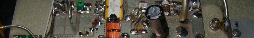
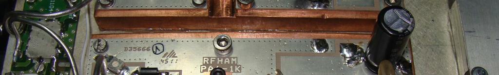
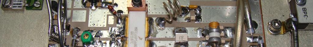
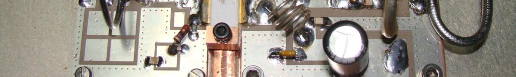
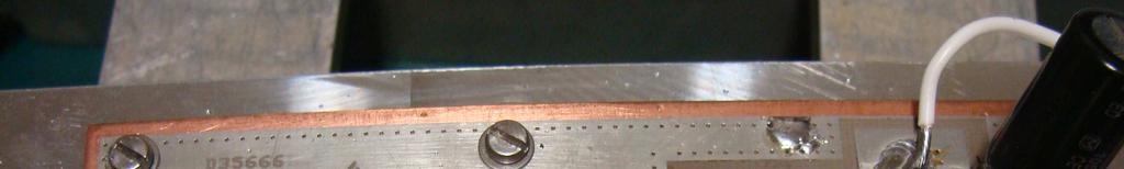
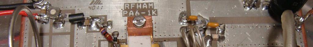
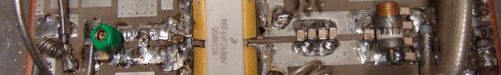
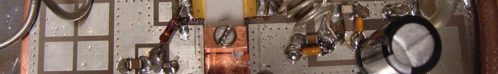
3 For other technical aspects, please refer to DUBUS issue 4 / 2010 vol 39 Compact 144 MHz High Power Solid State Amplifier using MRFE6VP61K25H from F1JRD/AE7KX 3. Amplifier design and performance The goal of this module is to be able to get 1 kw solid state, with good efficiency, small size, and good VSWRhandling into operation. The PCB for this pallet is the same as the 6 m pallet PA61K. For thermal aspect is referred to (1). The PCB is TC350 material, which has a very good RF and thermal performance. The size of the amplifier is 120 x 72 mm. The transistor has to dissipate more than 300 w in a small area, so a copper heat spreader is necessary to transfer the heat to the aluminum heat sink. Two techniques can be used to put the PCB on the copper heat spreader: With screws like in the picture, or with solder. This last technique needs some expertise and some solder paste (3). Circuit description: The input circuit is realized with 1:1 50Ω balun and a micro-strip matching lines towards the gates. The input matching is tuned by L1, and C6. The 500Ω trimmer can be removed if an external bias circuit is used. 1 K R2 and R4 are connected to ground to prevent a bias disconnection (if P1 is not in use) The output circuit uses also micro-strip lines and a 50Ω balun, made of 50Ω.141 coaxial cable. Particular attention has to be paid to soldering the capacitors C18,C9,C20,C21 (5.1 pf ATC 100 B or Temex CHB) (see the picture). One 18 pf high Q factor capacitor CLX series from TEMEX may replace the four 5.1 pf capacitors.. C23 is used to tune up for optimal efficiency. In this amplifier I didn t use a balancing wire. This can be done, and it will improve 2 nd harmonic suppression. 3
4 4. RF measurements of the 500 W pallet. RF measurements were performed in CW 50 V Drain supply, 1000 ma Idq (For linear operation): This test is performed with the amplifier pallet only, i.e. without filter. Freq (MHz) Pin (W) Pout (W) Gain (db) Drain Eff (%) PAE(%) * Vd (V) Id (A) dbc * PAE : Power Added Efficiency. This value includes the RF input power 5. RF measurements of the 1000 W module. 4
5 In order to get a kw brick we need to combine two pallets. Combining high powers is a precise issue and several techniques may be used. I have chosen to use a -3 db 90 hybrid coupler from Innovative using a IPP2102. This is an expensive part but very safe. This coupler is used to combine the two outputs of the two pallets. At the input I used a -3 db 90 hybrid coupler from Anaren XC Remco PA3FYM will describe in the next Dubus issue an alternative way to combine with a lower cost. RF measurements were performed in CW 50 V Drain supply, 2 x 1000 ma Idq (For linear operation): This test is done with the amplifier only (without filter) Pout Gain Drain Eff PAE(%) Id1(A) Id2(A) P power Freq (MHz) Pin (W) (W) (db) (%) * Vd (V) supply (W) dbc * PAE : Power Added Efficiency this value include the RF input power The harmonic test show - 47 dbc and - 83 dbc in 1296 MHz at 1 KW output power. A filter is absolutely necessary to get the harmonics below 60 dbc. Test with the filter The harmonic test show - 70 dbc and - 86 dbc in 1296 MHz at 1 KW output power. 5


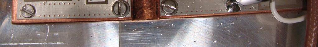
6 We have tested this amplifier with a filter, designed by F5CYS, based, on a F1TE design for 2 m (3), This filter has also a 2 m rejector to reduce the broadband noise in a multi VHF contest team. F5CYS 70 cm kw power filter 5. IMD measurement The IMD measure was done in the same conditions as the 2 m amplifier ( with 2 drivers ) Idq : 2 x 1A Pout : 1200 W PEP IMD3 : - 23 dbc / PEP Pout : 800 W PEP IMD3 : - 28 dbc / PEP Pout : 400 W PEP IMD3 : - 34 dbc / PEP 7. Ruggedness MRFE6VP5600H is a very rugged device, capable of handling 65:1 VSWR in pulse mode. It was designed for high mismatch applications, such as laser and plasma exciters, that exhibit repetitive high VSWR values at startup and then come back to a more friendly impedance. In CW, at these VSWR levels and rated powers, the limiting factor is the maximum DC power dissipation. A VSWR protection circuit that will shutdown the gate voltage to 0 or -3V within 10mS on a single shot, will protect the transistor effectively. The amplifier presented here was tested for all phase angles with 10mS pulses (5% duty cycle) without any failure or degradation in RF performance. In any case a protection circuit has to be used, like the ones described for the 6 m and 2 m amplifiers. A circulator can be used also, but is expensive. Construction : Layout and bill of material for one pallet. 6
 L4,L5 (Air inductor) Bead with wire Fair-Rite (95 ohm@100mhz) 6 Turn air inductor on 3 mm diameter, 3 Turn air inductor on 7 mm diameter, Tinned copper wire of")
7 Fixture layout and placement Tab1. Bill Of Materials B1 L1 (Air inductor) L4,L5 (Air inductor) Bead with wire Fair-Rite (95 6 Turn air inductor on 3 mm diameter, 3 Turn air inductor on 7 mm diameter, Tinned copper wire of 0.6 mm diameter Silver plated copper wire of 12/10mm diameter C1,C2,C3,C nf Ceramic Capacitor 100 V SMD C4,C5 39 pf Ceramic HQ Capacitor 100 B, CHB ATC, TEMEX Murata(RF electronica CVC- C 6 Trimming capacitor 3 to 30 pf Green 30) C7, C8 5.6 pf NPO or HQ SMD C9 4.7 pf NPO or HQ SMD C10,C11 33 pf Ceramic HQ Capacitor 100 A ATC, TEMEX C13,C14 1 nf NPO Ceramic Capacitor SMD C15,C pf to 1 nf Ceramic HQ Capacitor 100 B, CHB ATC, TEMEX C16,C nf 100 V Ceramic Capacitor LCC C18 18 pf Ceramic HQ capacitor CLX TEMEX Or C18,C19,C20,C pf Ceramic HQ Capacitor 100 B, CHB ATC, TEMEX Giga trimmer 1.3 to 16 pf Johanson (RF electronica C CVG-N1) C24 10 pf Ceramic HQ Capacitor 100 B, CHB ATC, TEMEX C24,C25,C26,C pf Ceramic HQ Capacitor 100 B, CHB ATC, TEMEX C17,C uf 160V C nf Ceramic Capacitor 100 V SMD R1,R5 47 ohm 1 W Power Resistor PR01 Vishay R2,R4 470 ohm 1/4 W Power Resistor 1206 Vishay 7


 mount SMD")

 mount")
8 R3 33 ohm 1/4 W Power Resistor 1206 Vishay P1 500 Ohms SMD pot Bourns Q1 MRFE6VP5600H Freescale Q2 78L05 TO92 Coax1 50 Ohm 11 cm SM.086 Huber & Suhner Coax2 50 Ohm 11 cm SM.141 Huber & Suhner PCB Arlon TC350, 2 OZ 30 mils PA6-1K RFham.com 1) mount SMD components 2) prepare the 1:1 input and output baluns 3) mount the PCB on the copper heat spreader. 8


9 9

 With a DVM (Digital Volt Meter) measure in the resistance between the gate pad and ground R = 30 Ω 9) Transistor")

 Use silicon grease (the white one for a lower thermal resistance) Before doing anything, the transistor has to be")

10 Note: I have tested this design also with the MRF6VP2600H, and it works perfectly. However, this device is more fragile than the 5600H In this version I used 4 x 5.1 pf with a small space in between. 8) Before soldering the transistor it is preferred to perform some small tests. a) Set the bias potentiometer to zero. b) With a DVM (Digital Volt Meter) measure in the resistance between the gate pad and ground R = 30 Ω 9) Transistor placement : Two techniques can be used: a) The transistor can be soldered. This technique is preferred to obtain a very low thermal resistance. Disadvantage is, when the transistor is destroyed for any reason it will be difficult to replace. b) Use silicon grease (the white one for a lower thermal resistance) Before doing anything, the transistor has to be prepared. As delivered, the flange of the transistor is not very flat. To improve the flatness, the best way is to use abrasive paper type 3 M 734 P1200. The abrasive paper has to be put on a very flat surface, like glass. Hold the transistor and make a shape of the number 8 with your hand until the flange is very flat. Mount the transistor. 10) Bias adjustment Connect the output to a 50Ω load. Use two power supplies: 10
11 One for the bias 0 to 12 V Set to 5 V (check if the bias potentiometer is set to ground!!) Set the drain power supply to 50 V and limit the current consumption to 2A. Adjust the drain current (Idq) up to 2A, i.e. each part of the LDMOS device draws 1A. 11) Small signal test: If you have a network analyzer or similar, test the amplifier in small signal mode, otherwise with very low input power. Connect the output of the amplifier to an appropriate dummy load. Tune the input VSWR by trimming L1 and C6. The input return loss should be better than 15 db. The small signal gain is around 28 db. If you do not get this values DO NOT drive the amplifier to full power, you may have a wrong output wiring. Double check the input and/or output circuits thoroughly. 12) High power test: A priori, these LDMOS devices are very sensitive towards overdrive. The best way to keep your transistor alive, is to attenuate the input power in all cases. Nowadays 432 MHz transceivers have output powers around 50 W. Of course the output power can be lowered to 1 W. But... if you forget, you will drive 50 W into the amplifier and destroy the transistors immediately. Note: Many amateur transceivers with power controls have a bad ALC and may transmit a big spike at the beginning of each transmission. Again, reduce the output power of your transceiver e.g. with a 10 db (power) attenuator or a long length of e.g. RG316 coaxial cable. Next step: Inject ca. 1 W into the amplifier, and ca. 200 W output power should be measured. Check the drain current: it has to be approximately 10 A. If it is not the case, stop and verify the output matching circuit (i.e. balun and the capacitors). If all works well, increase the input power until 500 W of output power is achieved (Pin = ~ 3.5W) and optimize the efficiency with C23. Also monitor and minimize the input VSWR. Repeat this for each 500 W pallet. Connect the two tested (and working!) pallets to both the input and output combiners. Inject sufficient drive (ca. 1.5W) to obtain ca. 200W output. Monitor the drain current: it should be around 14A. If it is not the case, stop and verify the combiner phases of both the input and output. If all works well, increase the input power to achieve 500 W output, and monitor the drain current: it has to be in the range of 23 A. The input power should be around 3.5W Increase the input power until 1 kw output is reached (input ca. 10W). The total drain current should be around 32A. Don t forget to use protection circuits. Several descriptions are available (3) (4) A kit of the main components of this amplifier is available (5). Conclusion This design was duplicated several times before publication of this article, and each amplifier showed similar results. However, be careful. High power amplifiers can be dangerous. 11
12 Many thanks to F1JRD Lionel, F1TE Lucien, F6BKI Jacques, Remco PA3FYM, Thomas Jann, F5VHX Graham I want to mention a special memory of Rainer DJ9BV who in the mid 90 s exchanged with me a lot of mail and discussion to create 1 kw 70 cm solid state. And also some special thanks to Dick K2RIW, he showed me his first (1970 s) K2RIW amplifier a kw on 70 cm when I visited him t10 years ago. References MRFE6VP5600H datasheet (1) A compact 144 MHz High Power Solid State Amplifier using the MRFE6VP6125KH by F1JRD (2) AN1034D Freescale (ex TRW application note) (3) ; (4) (5) (6) A compact 50 MHz High Power Solid State Amplifier using the MRFE6VP6125KH by F5FLN 12
Compact 50 MHz High Power Solid State Amplifier using MRFE6VP61K25H
 Compact 50 MHz High Power Solid State Amplifier using MRFE6VP61K25H By F5FLN Michel ROUSSELET and F1TE Lucien SERRANO, F6BKI Jacques RAMBAUD November 2011 Rev1 This Article deals with RF amplifier design
HAM RADIO. 1 KW SSPA 144 MHz RF POWER AMPLIFIER SWR 65:1
 AMD 1000 AR 144 November 2011 First Edition HAM RADIO 1 KW SSPA 144 MHz RF POWER AMPLIFIER SWR 65:1 RF Dispositive : MRF6VP61K25HR6 Freescale Frequency Range 142-146 MHz 4 W Input ± 0.5 W ( @ 1 KW Carrier
MHz (FM BAND) 50 Volts Input/output 50 ohms Pout: 1250W minimum Up to 85% efficiency 22dB Gain NXP MRF1K50 Mosfet Planar RF Transformers
 50 Volts Input/output 50 ohms Pout: 1250W minimum Up to 85% efficiency 22dB Gain NXP MRF1K50 Mosfet Planar RF Transformers") Model MRF1K50-PLA FM Pallet Amplifier This amplifier module is ideal for final output stages in FM Broadcast Applications. 87.5 108.1MHz (FM BAND) 50 Volts Input/output 50 ohms Pout: 1250W minimum Up to
Model MRF1K50-PLA FM Pallet Amplifier This amplifier module is ideal for final output stages in FM Broadcast Applications. 87.5 108.1MHz (FM BAND) 50 Volts Input/output 50 ohms Pout: 1250W minimum Up to
MHz (FM BAND) 50 Volts Input/output 50 ohms Pout: 1000W minimum Up to 85% efficiency 24dB Gain NXP BLF188XR Mosfet Planar RF Transformers
 50 Volts Input/output 50 ohms Pout: 1000W minimum Up to 85% efficiency 24dB Gain NXP BLF188XR Mosfet Planar RF Transformers") Model P1000FM-188PLA FM Pallet Amplifier This amplifier module is ideal for final output stages in FM Broadcast Applications. 87.5 108.1MHz (FM BAND) 50 Volts Input/output 50 ohms Pout: 1000W minimum Up
Model P1000FM-188PLA FM Pallet Amplifier This amplifier module is ideal for final output stages in FM Broadcast Applications. 87.5 108.1MHz (FM BAND) 50 Volts Input/output 50 ohms Pout: 1000W minimum Up
600W HAM RADIO 2M/144Mhz POWER AMPLIFIER MODULE
 Designed for 2M/144Mhz radio transposers and transmitters, this amplifier incorporates LDMOS transistors to enhance ruggedness and reliability. General characteristics: 140-148 MHz. 48 Volts. Internal
MHz (FM BAND) 50 Volts Input/output 50 ohms Pout: 1000W minimum 78% 23dB Gain NXP BLF184XR Mosfet
 50 Volts Input/output 50 ohms Pout: 1000W minimum 78% 23dB Gain NXP BLF184XR Mosfet") Model P600FM-184XR FM Pallet Amplifier This amplifier module is ideal for final output stages in FM Broadcast Applications. 87.5 108.1MHz (FM BAND) 50 Volts Input/output 50 ohms Pout: 1000W minimum 78%
Model P600FM-184XR FM Pallet Amplifier This amplifier module is ideal for final output stages in FM Broadcast Applications. 87.5 108.1MHz (FM BAND) 50 Volts Input/output 50 ohms Pout: 1000W minimum 78%
A 3 Watt LDMOS Driver for the 432MHz band
 A 3 Watt LDMOS Driver for the 432MHz band John C Worsnop. PhD CEng MIET, G4BAO Introduction The popularity of my 2.5-Watt driver kit for the 1296MHz band (1) and the recent publication of G4DDK s Iceni
RF Power LDMOS Transistor High Ruggedness N--Channel Enhancement--Mode Lateral MOSFET
 Technical Data RF Power LDMOS Transistor High Ruggedness N--Channel Enhancement--Mode Lateral MOSFET RF power transistor designed for both narrowband and broadband ISM, broadcast and aerospace applications
200 W, 32 V HF to 1.3 GHz LDMOS transistor in a STAC package. Features. Description. Table 1. Device summary. Order code Marking Package Packaging
 200 W, 32 V HF to 1.3 GHz LDMOS transistor in a STAC package Features Datasheet - preliminary data Figure 1. Pin connection 1 STAC244B Air cavity 1 2 Improved ruggedness: V (BR)DSS > 80 V Load mismatch
1208 P10-VHF-H-20. Frequency Range: MHz. Efficiency: 10% Temperature Range: 0 to 70 C Max VSWR: 5:1. Class: Supply Voltage: 28.
 Part Number Revision 2.C Release Date July 24, 2007 Revision Notes Included Mechanical Drawings Amplifier Name Technical Specifications Summary Frequency Range: 170-230 MHz P1dB: 10 Watts CW Class: A Supply
G6ALU 20W FET PA Construction Information
 G6ALU 20W FET PA Construction Information The requirement This amplifier was designed specifically to complement the Pic-A-Star transceiver developed by Peter Rhodes G3XJP. From the band pass filter an
RF Power LDMOS Transistors High Ruggedness N--Channel Enhancement--Mode Lateral MOSFETs
 Freescale Semiconductor Technical Data Document Number: MRFE6VP5300N Rev. 1, 6/2014 RF Power LDMOS Transistors High Ruggedness N--Channel Enhancement--Mode Lateral MOSFETs These high ruggedness devices
***note: pallet may draw up to 5.0 amps on a 32V supply.
 Model BCI-UHF-40TX12 TV Pallet Amplifier Module This amplifier module is ideal for final output stages in analog and digital TV broadcast equipment. 470 860MHz 28-32 Volts Pout: 25W Peak Sync. 10Watts
Revision 1.b Release Date July 29, 2007 This data sheet covers models 4379, 4472 Revision Notes Repl 0.d (Rev p/n 250W, B version of Comb)
") Part Number Revision 1.b Release Date July 29, 2007 This data sheet covers models 4379, 4472 Revision Notes Repl 0.d (Rev p/n 250W, B version of Comb) Amplifier Name Technical Specifications Summary Frequency
Part Number Revision 1.b Release Date July 29, 2007 This data sheet covers models 4379, 4472 Revision Notes Repl 0.d (Rev p/n 250W, B version of Comb) Amplifier Name Technical Specifications Summary Frequency
Watts W/ C Storage Temperature Range Tstg 65 to +200 C Operating Junction Temperature TJ 200 C. Test Conditions
 SEMICONDUCTOR TECHNICAL DATA The RF Sub Micron MOSFET Line N Channel Enhancement Mode Lateral MOSFETs Designed for broadband commercial and industrial applications at frequencies in the 865 895 MHz band.
RF Power LDMOS Transistors High Ruggedness N--Channel Enhancement--Mode Lateral MOSFETs
 Freescale Semiconductor Technical Data RF Power LDMOS Transistors High Ruggedness N--Channel Enhancement--Mode Lateral MOSFETs RF power transistors suitable for both narrowband and broadband CW or pulse
4W CW, MHz Power Transistor
 4W CW, 30-2700 Power Transistor FEATURES Frequency: 30-2700 Gain @ 900Mhz: 16.5dB Psat @ 900: 37dBm PAE @ Psat: 47% @ 900 15-28V Operation DESCRIPTION The is a broadband capable 4W GaN on Silicon power
QPD W, 28V, GHz, GaN RF Input-Matched Transistor
 Product Overview The Qorvo is a W (P3dB), 50Ω-input matched discrete GaN on SiC HEMT which operates from 30MHz to 1.2 GHz. The integrated input matching network enables wideband gain and power performance,
Features. Description. Table 1: Device summary Order code Marking Package Packing SD2932W SD2932 (1) M244 Tube
 M244 Tube") HF/VHF/UHF RF power N-channel MOSFET Datasheet - production data Features Gold metallization Excellent thermal stability Common source push-pull configuration POUT = 300 W min. with 15 db gain @ 175 MHz
HF/VHF/UHF RF power N-channel MOSFET Datasheet - production data Features Gold metallization Excellent thermal stability Common source push-pull configuration POUT = 300 W min. with 15 db gain @ 175 MHz
RF Power LDMOS Transistors N--Channel Enhancement--Mode Lateral MOSFETs
 Freescale Semiconductor Technical Data RF Power LDMOS Transistors N--Channel Enhancement--Mode Lateral MOSFETs These high ruggedness devices are designed for use in high VSWR military, aerospace and defense,
Frequency Range: MHz. Efficiency: 10% Temperature Range: 0 to 60 C Max VSWR: 5:1. Class: Supply Voltage: 28.0V
 Part Number Revision 1.c Release Date July 24, 2007 Revision Notes Amplifier Name Technical Specifications Summary Frequency Range: 50-88 MHz P1dB: 60 Watts CW Class: A Supply Voltage: 28.0V Gain: 36dB
RF Power LDMOS Transistors High Ruggedness N--Channel Enhancement--Mode Lateral MOSFETs
 Technical Data Document Number: MRF101AN Rev. 0, 11/18 RF Power LDMOS Transistors High Ruggedness N--Channel Enhancement--Mode Lateral MOSFETs These devices are designed for use in VHF/UHF communications,
50 V moisture resistant DMOS transistor for ISM applications. Features. Description. Table 1. Device summary
 50 V moisture resistant DMOS transistor for ISM applications Features Datasheet - production data M177MR Epoxy sealed Figure 1. Pin connection 3 4 1 2 5 Improved ruggedness V (BR)DSS > 200 V Excellent
1562 P150-UHF-13. Frequency Range: MHz. Efficiency: 45% Temperature Range: 0 to 70 C Max VSWR: 1.5:1. Supply Voltage: 32.
 1562 Part Number P150-UHF-13 Amplifier Name 1562 P150-UHF-13 Revision 1.f Release Date July 9th 2007 Revision Notes Frequency Range: 470-860 MHz P1dB: 55 Watts CW Class: AB Supply Voltage: 32.0V Gain:
SD56120M RF POWER TRANSISTORS The LdmoST FAMILY
 RF POWER TRANSISTORS The LdmoST FAMILY N-CHANNEL ENHANCEMENT-MODE LATERAL MOSFETs EXCELLENT THERMAL STABILITY COMMON SOURCE CONFIGURATION, PUSH- PULL P OUT = 120 W WITH 13 db gain @ 860 MHz /32V BeO FREE
Rating Symbol Value Unit Drain Source Voltage VDSS 65 Vdc Drain Gate Voltage (RGS = 1.0 MΩ)
") SEMICONDUCTOR TECHNICAL DATA Order this document by MRF275G/D The RF MOSFET Line N Channel Enhancement Mode Designed primarily for wideband large signal output and driver stages from 1 5 MHz. Guaranteed
SEMICONDUCTOR TECHNICAL DATA Order this document by MRF275G/D The RF MOSFET Line N Channel Enhancement Mode Designed primarily for wideband large signal output and driver stages from 1 5 MHz. Guaranteed
RF Power LDMOS Transistor N--Channel Enhancement--Mode Lateral MOSFET
 Freescale Semiconductor Technical Data RF Power LDMOS Transistor N--Channel Enhancement--Mode Lateral MOSFET Designed primarily for CW large--signal output and driver applications with frequencies up to
SSPA Construction Techniques
 SSPA Construction Techniques 6m, 2m, 222MHz, 70cm 23cm and above 1.8 54MHz digressed a bit at mentioning 1.8-54, didn t I? September 2016 Austin BBQ, 2016 1 But Wait Let s examine how to build that SSPA
Frequency Range: MHz. Efficiency: 80% Temperature Range: -20 to 65 C Max VSWR: 3:1. Class: Supply Voltage: 32.0V
 Part Number Revision 0.B Release Date October 19, 2007 Revision Notes Final production release Amplifier Name Technical Specifications Summary Frequency Range: 86-108 MHz P1dB: 500 Watts CW Class: C Supply
TB263 Frequency=30-512MHz Pout=180W Gain= dB Vds=28Vdc Idq=0.5A Efficiency=56-70% LS2641
 TB263 Frequency=-512MHz Pout=18W Gain=16.87-2.51dB Vds=28Vdc Idq=.5A Efficiency=56-7% LS2641 Order of Operations: 1. Review amplifier s performance curves in the data package to learn its RF power limitations.
RF Power LDMOS Transistors High Ruggedness N--Channel Enhancement--Mode Lateral MOSFETs
 Technical Data RF Power LDMOS Transistors High Ruggedness N--Channel Enhancement--Mode Lateral MOSFETs These high ruggedness devices are designed for use in high VSWR industrial, medical, broadcast, aerospace
VSWR Testing of RF Power MOSFETs
 VSWR Testing of RF Power MOSFETs Application Note 1820 Overview No amplifier designed for 50Ω will always see a 50Ω load. Things go wrong, mistakes are made. In some applications the amplifier qualification
TB266 Frequency=1.5-30MHz Pout=150W Gain=21-23dB Vds=24Vdc Idq=1.5A Efficiency=52-53% LS2541HF
 TB266 Frequency=1.5-30MHz Pout=150W Gain=21-23dB Vds=24Vdc Idq=1.5A Efficiency=52-53% LS2541HF Order of Operations: 1. Review amplifier s performance curves in the data package to learn its RF power limitations.
PA FAN PLATE ASSEMBLY 188D6127G1 SYMBOL PART NO. DESCRIPTION. 4 SBS /10 Spring nut. 5 19A702339P510 Screw, thread forming, flat head.
 MAINTENANCE MANUAL 851-870 MHz, 110 WATT POWER AMPLIFIER 19D902797G5 TABLE OF CONTENTS Page DESCRIPTION.............................................. Front Page SPECIFICATIONS.................................................
T1G FS 30W, 28V, DC 6 GHz, GaN RF Power Transistor
 Applications Military radar Civilian radar Professional and military radio communications Test instrumentation Wideband or narrowband amplifiers Jammers Product Features Frequency: DC to 6 GHz Output Power
4662 P250-UHF-14-A. Frequency Range: MHz. Efficiency: 38% Temperature Range: -10 to 55 C Max VSWR: 3:1. Supply Voltage: 32.
 Part Number Revision 0.B Release Date November 5, 2007 This data sheet applies to models 4662, 4978 Revision Notes Updated Mechanical information. Revised Specification (formal production release) Amplifier
12.5W CW, MHz Power Transistor
 Preliminary Specification 12.5W CW, 2-3MHz Power Transistor FEATURES Frequency: 2-3MHz Gain @ 8Mhz: 17dB Psat @ 8MHz: 42dBm PAE @ Psat: 52% @ 8MHz 28V Operation DESCRIPTION The is a broadband capable 12.5W
Efficiency: 68% Temperature Range: +0 to 60 C Max VSWR: 5:1. Class: Supply Voltage:
 Part Number Revision 2.C Release Date July 11 2007 Revision Notes - updated new format Amplifier Name Technical Specifications Summary Frequency Range: P1dB: Class: Supply Voltage: 88-108 MHz 750 Watts
RF Power LDMOS Transistors High Ruggedness N--Channel Enhancement--Mode Lateral MOSFETs
 Freescale Semiconductor Technical Data RF Power LDMOS Transistors High Ruggedness N--Channel Enhancement--Mode Lateral MOSFETs RF power transistors suitable for both narrowband and broadband CW or pulse
SD4933. HF/VHF/UHF RF power N-channel MOSFET. Features. Description
 HF/VHF/UHF RF power N-channel MOSFET Features Datasheet - production data Improved ruggedness V (BR)DSS > 200 V Excellent thermal stability 20:1 all phases load mismatch capability P OUT = 300 W min. with
Absolute Maximum Ratings Parameter Rating Unit Drain Voltage (V D ) 150 V Gate Voltage (V G ) -8 to +2 V Gate Current (I G ) 39 ma Operational Voltage
 150 V Gate Voltage (V G ) -8 to +2 V Gate Current (I G ) 39 ma Operational Voltage") 60W GaN WIDEBAND POWER AMPLIFIER Package: Hermetic 2-Pin Flanged Ceramic Features Broadband Operation DC to 3.5GHz Advanced GaN HEMT Technology Advanced Heat-Sink Technology Small Signal Gain = db at 2GHz
60W GaN WIDEBAND POWER AMPLIFIER Package: Hermetic 2-Pin Flanged Ceramic Features Broadband Operation DC to 3.5GHz Advanced GaN HEMT Technology Advanced Heat-Sink Technology Small Signal Gain = db at 2GHz
GaAs MMIC Power Amplifier
 GaAs MMIC Power Amplifier AM153040WM-BM-R AM153040WM-FM-R Aug 2010 Rev 0 DESCRIPTION AMCOM s is part of the GaAs HiFET MMIC power amplifier series. It is a 2-stage GaAs HIFET PHEMT MMIC power amplifier.
AGR09085E 85 W, 865 MHz 895 MHz, N-Channel E-Mode, Lateral MOSFET
 Introduction The AGR09085E is a high-voltage, laterally diffused metal oxide semiconductor (LDMOS) RF power transistor suitable for cellular band, code division multiple access (CDMA), global system for
RF Power LDMOS Transistors High Ruggedness N--Channel Enhancement--Mode Lateral MOSFETs
 Freescale Semiconductor Technical Data RF Power LDMOS Transistors High Ruggedness N--Channel Enhancement--Mode Lateral MOSFETs Designed for mobile two--way radio applications with frequencies from 136
4454 P500-UHF-17-A. Frequency Range: MHz. Efficiency: 36% Temperature Range: -10 to 55 C Max VSWR: 3:1. Supply Voltage: 32.
 Part Number Revision 0.e Release Date December 13, 2007 This document applies to 4454 and 5029 Revision Notes: 0.b Full production release, Apr 07. 0.c Revised Specs May 07. Revised Integration Instructions
RF Power LDMOS Transistors High Ruggedness N--Channel Enhancement--Mode Lateral MOSFETs
 Freescale Semiconductor Technical Data RF Power LDMOS Transistors High Ruggedness N--Channel Enhancement--Mode Lateral MOSFETs These high ruggedness devices are designed for use in high VSWR industrial
RF Power LDMOS Transistor High Ruggedness N--Channel Enhancement--Mode Lateral MOSFET
 Technical Data RF Power LDMOS Transistor High Ruggedness N--Channel Enhancement--Mode Lateral MOSFET This high ruggedness device is designed for use in high VSWR industrial, medical, broadcast, aerospace
REAL Solid State Power at VHF / UHF
 REAL Solid State Power at VHF / UHF Barry Malowanchuk VE4MA Microwave Update Conference, October 2012 1 REAL Solid State Power at VHF/ UHF New Power Transistor Technology Replacements for 2 x 4CX250 s
Low Pass Filter (rev 5) for single and 2-Pallet HF Amplifiers The filter sections on this board differ from the web article, and offer some
 for single and 2-Pallet HF Amplifiers The filter sections on this board differ from the web article, and offer some") The filter sections on this board differ from the web article, and offer some improvement in performance, including raising the maximum power handling capacity. The most significant changes were to the
The filter sections on this board differ from the web article, and offer some improvement in performance, including raising the maximum power handling capacity. The most significant changes were to the
T2G Q3 10W, 28V DC 6 GHz, GaN RF Power Transistor
 Applications Military radar Civilian radar Professional and military radio communications Test instrumentation Wideband or narrowband amplifiers Jammers Product Features Frequency: DC to 6 GHz Output Power
RF Power LDMOS Transistors N--Channel Enhancement--Mode Lateral MOSFETs
 Technical Data RF Power LDMOS Transistors N--Channel Enhancement--Mode Lateral MOSFETs These 750 W CW transistors are designed for industrial, scientific and medical (ISM) applications in the 700 to 1300
QPD W, 50V, DC 4 GHz, GaN RF Transistor
 General Description The Qorvo QPD1010 is a 10 W (P3dB) discrete GaN on SiC HEMT which operates from DC to 4 GHz. The device is constructed with Qorvo s proven QGaN25HV process, which features advanced
IS-95, 9 Ch Fwd, Offset=750KHz, ACPR Integrated Bandwidth, ACPR=-55dB
 Product Description Sirenza Microdevices SLD-283CZ is a robust 12 Watt high performance LDMOS transistor designed for operation to 27MHz. It is an excellent solution for applications requiring high linearity
T1G Q3 DC 6 GHz 18 W GaN RF Power Transistor
 Applications General Purpose RF Power Jammers Military and Civilian Radar Professional and Military radio systems Wideband amplifiers Test instrumentation Avionics Product Features Frequency: DC to 6 GHz
RF Power LDMOS Transistors N--Channel Enhancement--Mode Lateral MOSFETs
 Preliminary Data Document Number: Order from RF Marketing Rev. 1.0, 09/2017 RF Power LDMOS Transistors N--Channel Enhancement--Mode Lateral MOSFETs These 750 W CW transistors are designed for industrial,
AN1224 Application note
 Application note Evaluation board using SD57045 LDMOS RF transistor for FM broadcast application Introduction LDMOS technology allows the manufacturing of high efficiency and high gain amplifiers for FM
RFM HSD MHz 350W Class A/AB High Performance Amplifier with High Speed Disable
 Class A/AB 350W linear amplifier Fast output disable,
Model FM350 FM Broadcast Pallet Amplifier
 Model FM350 FM Broadcast Pallet Amplifier Designed for FM radio transmitters, this amplifier incorporates the latest technology from ST Microelectronics. (Formerly known as SGS Thompson). 86 110MHz 48
TGA2601-SM MHz High IP3 Dual phemt. Key Features and Performance. Measured Performance. Primary Applications. Product Description
 800-3000 MHz High IP3 Dual phemt Key Features and Performance 800-3000 MHz Frequency Range
ATF-531P8 E-pHEMT GaAs FET Low Noise Amplifier Design for 800 and 900 MHz Applications. Application Note 1371
 ATF-31P8 E-pHEMT GaAs FET Low Noise Amplifier Design for 8 and 9 MHz Applications Application Note 1371 Introduction A critical first step in any LNA design is the selection of the active device. Low cost
GaAs MMIC devices are susceptible to Electrostatic Discharge. Use proper ESD precautions when handling these items.
 The is a broadband, power efficient GaAs PHEMT distributed amplifier in a 4mm QFN surface mount package. The is designed to provide optimal LO drive for T3 mixers. Typically, ADM-26-2931SM provides. db
GaAs MMIC devices are susceptible to Electrostatic Discharge. Use proper ESD precautions when handling these items.
 ADM-26-929SM The ADM-26-929SM is a broadband, efficient GaAs PHEMT distributed amplifier in a 4mm QFN surface mount package. It is designed to provide optimal LO drive for T3 mixers and offers 13 db typical
Features. Description. Table 1: Device summary Order code Marking Package Packing SD2942W SD2942 (1) M244 Tube
 M244 Tube") HF/VHF/UHF RF power N-channel MOSFET Datasheet - production data Features Gold metallization Excellent thermal stability Common source push-pull configuration POUT = 350 W min. with 15 db gain @ 175 MHz
HF/VHF/UHF RF power N-channel MOSFET Datasheet - production data Features Gold metallization Excellent thermal stability Common source push-pull configuration POUT = 350 W min. with 15 db gain @ 175 MHz
DB RF power amplifier using PD85025-E for UHF OFDM radio. Features. Description
 RF power amplifier using PD85025-E for UHF OFDM radio Features Excellent thermal stability Frequency: 340-520 MHz Supply voltage: 15 V Output power: 10 WPEP Gain: 19 ± 1 db Efficiency: 45 % - 52 % Load
2-Tone Generator For 145Mhz
 Wolfgang Schneider, DJ8ES 2-Tone Generator For 145Mhz An RF amplifier stage is not only classified by amplification, which is as high as possible, and thus by its maximum output. What is frequently not
MITSUBISHI RF MOSFET MODULE
 MITSUBISHI RF MOSFET MODULE 135-175MHz 8W 12.5V PORTABLE/MOBILE RADIO DESCRIPTION The is a 8-watt RF MOSFET Amplifier Module for 12.5-volt portable/ mobile radios that operate in the 135- to 175-MHz range.
QPD W, 50V, DC 3.7 GHz, GaN RF Transistor
 General Description The is a 65 W (P3dB) wideband unmatched discrete GaN on SiC HEMT which operates from DC to 3.7 GHz and a V supply rail. The device is in an industry standard air cavity package and
TGA2818-SM S-Band 30 W GaN Power Amplifier
 S-Band 3 W GaN Power Amplifier Applications Military Radar Civilian Radar Wideband Amplifiers Product Features Functional Block Diagram Frequency Range: 2.8-3.7 GHz Pout: >.5 dbm (Pin=27 dbm) Large Signal
17-35GHz MPA/Multiplier TGA4040SM
 Not Recommended for New Designs Advance Product Information 17-35GHz MPA/Multiplier TriQuint Recommends the TGA43-SM or TGA431-SM be used for New Designs Key Features Product Description The TriQuint TG44SM
RFM XR. 2-30MHz 500W Class AB Linear High Performance Amplifier. Maximum Ratings Operation beyond these ratings will void warranty.
 Class AB 500W XR-rated linear amplifier 2-30MHz bandwidth 27dB typical gain 64% typical efficiency +/- 1.1dB typical gain flatness Temperature-compensated bias TTL disable The RFP2-30-500XR is an XR-rated
TGA2602-SM MHz High IP3 Dual phemt. Key Features and Performance. Measured Performance. Primary Applications. Product Description
 800-3000 MHz High IP3 Dual phemt Key Features and Performance 800-3000 MHz Frequency Range
RF Power LDMOS Transistors High Ruggedness N--Channel Enhancement--Mode Lateral MOSFETs
 Freescale Semiconductor Technical Data RF Power LDMOS Transistors High Ruggedness N--Channel Enhancement--Mode Lateral MOSFETs These 1300 W RF power transistors are designed for applications operating
25W Power Packaged Transistor. GaN HEMT on SiC
 25W Power Packaged Transistor GaN HEMT on SiC Description The is an unmatched packaged Gallium Nitride High Electron Mobility Transistor. It offers general purpose and broadband solutions for a variety
ital mec PAFM0600A Objective data sheet Power Amplifier Section 600W FM Absolute maximum ratings Electrical Specifications
 Power Amplifier Section 600W FM Designed primarily for FM application, with a reliable Power Ldmos device. This amplifier is suitable for any CW or pulsed application. Output power detector and temperature
SLD-1083CZ 4 Watt Discrete LDMOS FET in Ceramic Package
 Product Description Sirenza Microdevices SLD-183CZ is a robust 4 Watt high performance LDMOS transistor designed for operation from to 27MHz. It is an excellent solution for applications requiring high
RF LDMOS Wideband Integrated Power Amplifier
 Freescale Semiconductor Technical Data Document Number: Rev. 0, 1/2016 RF LDMOS Wideband Integrated Power Amplifier The is a 2--stage, high gain amplifier designed to provide a high level of flexibility
RF Power LDMOS Transistors N--Channel Enhancement--Mode Lateral MOSFETs
 Technical Data RF Power LDMOS Transistors N--Channel Enhancement--Mode Lateral MOSFETs These RF power transistors are designed for pulse applications operating at 1030 to 1090 MHz and can be used over
The Design of A 125W L-Band GaN Power Amplifier
 Sheet Code RFi0613 White Paper The Design of A 125W L-Band GaN Power Amplifier This paper describes the design and evaluation of a single stage 125W L-Band GaN Power Amplifier using a low-cost packaged
RF Power LDMOS Transistor N--Channel Enhancement--Mode Lateral MOSFET
 Freescale Semiconductor Technical Data RF Power LDMOS Transistor N--Channel Enhancement--Mode Lateral MOSFET This 600 W RF power LDMOS transistor is designed primarily for wideband RF power amplifiers
TGA2214-CP 2 18 GHz 4 W GaN Power Amplifier
 Product Description Qorvo s TGA2214-CP is a packaged wideband power amplifier fabricated on Qorvo s QGaN15 0.15 µm GaN on SiC process. Operating from 2 to 18 GHz, the TGA2214- CP generates > 4 W saturated
GaAs MMIC devices are susceptible to Electrostatic Discharge. Use proper ESD precautions when handling these items.
 ADM-26-931SM The ADM-26-931SM is a broadband, power efficient GaAs PHEMT distributed amplifier in a 4mm QFN surface mount package. The ADM-26-931SM is designed to provide optimal LO drive for T3 mixers.
RF Power LDMOS Transistors High Ruggedness N--Channel Enhancement--Mode Lateral MOSFETs
 Technical Data RF Power LDMOS Transistors High Ruggedness N--Channel Enhancement--Mode Lateral MOSFETs These high ruggedness devices are designed for use in high VSWR industrial, scientific and medical
RF Power LDMOS Transistor High Ruggedness N--Channel Enhancement--Mode Lateral MOSFET
 Freescale Semiconductor Technical Data RF Power LDMOS Transistor High Ruggedness N--Channel Enhancement--Mode Lateral MOSFET This high ruggedness device is designed for use in high VSWR industrial, scientific
Many applications. Mismatched Load Characterization for High-Power RF Amplifiers PA CHARACTERIZATION. This article discusses the
 From April 2004 High Frequency Electronics Copyright 2004 Summit Technical Media, LLC Mismatched Load Characterization for High-Power RF Amplifiers By Richard W. Brounley, P.E. Brounley Engineering Many
GaAs MMIC devices are susceptible to Electrostatic Discharge. Use proper ESD precautions when handling these items.
 ADM-12-931SM The ADM-12-931SM is a small, low power, and economical T3 driver or T3A pre-amplifier. It is a GaAs PHEMT distributed amplifier in a 3mm QFN surface mount package. The ADM-12-931SM can provide
FP2189. Functional Diagram. Product Description. Product Features. Applications. Typical Performance (5) Specifications. Absolute Maximum Rating
 Specifications. Absolute Maximum Rating") FP89 -Watt HFET Product Features 5 MHz +3 dbm PdB +3 dbm Output IP3 High Drain Efficiency 8.5 db @ 9 MHz Lead-free/Green/RoHS-compliant SOT-89 Package MTTF > Years Applications Mobile Infrastructure CATV
FP89 -Watt HFET Product Features 5 MHz +3 dbm PdB +3 dbm Output IP3 High Drain Efficiency 8.5 db @ 9 MHz Lead-free/Green/RoHS-compliant SOT-89 Package MTTF > Years Applications Mobile Infrastructure CATV
GaAs MMIC Power Amplifier
 GaAs MMIC Power Amplifier AM324036WM-BM-R AM324036WM-FM-R Aug 10 Rev 6 DESCRIPTION AMCOM s is part of the GaAs MMIC power amplifier series. It has 29dB gain and 36dBm output power over the 3.2 to 4.0GHz
RF Power LDMOS Transistor N--Channel Enhancement--Mode Lateral MOSFET
 Freescale Semiconductor Technical Data RF Power LDMOS Transistor N--Channel Enhancement--Mode Lateral MOSFET This 12.5 W CW high efficiency RF power transistor is designed for consumer and commercial cooking
MGA HP GHz 12W High Efficiency GaN Power Amplifier Data Sheet
 Features: 13 db Gain 41 dbm and LSG 10 db CW OIP3 54 dbm at 34 dbm per tone PAE 46% at 42 dbm Matched Input and Output for Easy Cascade Surface Mount Package with RoHS Compliance Thermal Resistance is
40W Power Packaged Transistor. GaN HEMT on SiC
 Gain (db), Pout (dbm) & PAE (%) Id (A) Description 40W Power Packaged Transistor The is an unmatched packaged Gallium Nitride High Electron Mobility Transistor. It offers general purpose and broadband
QPD GHz, 110 W / 220 W, 48 V, Asymmetric Doherty
 Product Description The is an asymmetric Doherty power device composed of pre-matched, discrete GaN on SiC HEMTs. The device operates from 2.5 to 2.7 GHz. can deliver PAVG of 50 W at +48 V operation. ROHS
QPD1015L 65W, 50V, DC 3.7 GHz, GaN RF Transistor
 QPD15L General Description The QPD15L is a 65 W (P3dB) wideband unmatched discrete GaN on SiC HEMT which operates from DC to 3.7 GHz with a V supply rail. The device is in an industry standard air cavity
QPD1008L 125W, 50V, DC 3.2 GHz, GaN RF Transistor
 QPD8L General Description The QPD8L is a 125 W (P3dB) wideband unmatched discrete GaN on SiC HEMT which operates from DC to 3.2 GHz with a V supply rail. The device is in an industry standard air cavity
TGA2813-CP 3.1 to 3.6 GHz, 100W GaN Power Amplifier
 Applications Radar Product Features Frequency Range: 3.1 3.6 GHz Pout: 5 dbm (at PIN = 27 dbm) Power Gain: 23 db (at PIN = 27 dbm) PAE: 51 % CW Bias: VD = pulsed (PW = 15 ms, DC = 3 %), IDQ = 3 ma, VG
TB269 Frequency= MHz Pout=250W Gain=18.0dB Vds=28Vdc Idq=1.1A 56% Efficiency LS2641
 TB269 Frequency=38-5MHz Pout=25W Gain=18.dB Vds=28Vdc Idq=1.1A 56% Efficiency LS2641 Order of Operations: 1. Review amplifier s performance curves in the data package to learn its RF power limitations.
PD55008 PD55008S RF POWER TRANSISTORS The LdmoST Plastic FAMILY
 PD55 PD55S RF POWER TRANSISTORS The LdmoST Plastic FAMILY N-CHANNEL ENHANCEMENT-MODE LATERAL MOSFETs EXCELLENT THERMAL STABILITY COMMON SOURCE CONFIGURATION P OUT = W with 17 db gain @ /.5V NEW RF PLASTIC
MITSUBISHI RF MOSFET MODULE
 MITSUBISHI RF MOSFET MODULE -7MHz 7W 7.V, Stage Amp. For PORTABLE RADIO DESCRIPTION The is a 7-watt RF MOSFET Amplifier Module for 7.-volt portable radios that operate in the - to 7-MHz range. The battery
QPD W, 50V, DC 4 GHz, GaN RF Transistor
 General Description The Qorvo is a W (P3dB) discrete GaN on SiC HEMT which operates from DC to 4 GHz. The device is constructed with Qorvo s proven QGaN25HV process, which features advanced field plate
TGA2578-CP 2 to 6 GHz, 30W GaN Power Amplifier
 2 to, W GaN Power Amplifier Applications Electronic Warfare Radar Communications Test Instrumentation EMC Amplifier Product Features Frequency Range: 2 Pout: dbm at PIN = 23 dbm PAE: >% CW Small Signal
TGA2612-SM 6 12 GHz GaN LNA
 Product Description Qorvo s is a packaged broadband Low Noise Amplifier fabricated on Qorvo s QGaN 0.um GaN on SiC process. Covering 6, the TGA2612- SM typically provides >23 dm small signal gain, 19 dbm