PHW Position Pinhole Wheel
|
|
|
- Rosalind Williams
- 5 years ago
- Views:
Transcription


1 P R E C I S I O N P I N H O L E S A N D P I N H O L E W H E E L Standard and High-Power Precision Pinholes Mounted in Ø1" Disks Single Pinhole Sizes from Ø1 μm to Ø1 mm 16-Position Pinhole Wheel with Hole Sizes from Ø25 µm to Ø2 mm P25CH High-Power 25 µm Pinhole Back View Front View P5H 5 µm Pinhole PHW16 16-Position Pinhole Wheel Application Idea P5H Ø5 µm Pinhole Mounted in SM1ZM Zoom Housing d ST1XY D XY T l t Hide Overview O V E R V I E W Features Mounted Precision Pinholes from Ø1 µm to Ø1 mm Mounted High-Power Pinholes from Ø10 µm to Ø50 µm Chrome-Plated Fused Silica Pinhole Wheel with 16 Pinholes from Ø25 µm to Ø2 mm Single Precision Pinholes Single mounted precision pinholes are available with pinhole diameters from 1 µm to 1 mm. We also offer high-power versions with pinhole diameters from 10 µm to 50 µm. For many applications, such as holography, spatial intensity variations in the laser beam are unacceptable. Using precision pinholes in conjunction with positioning and focusing equipment such as our KT310(/M) Spatial Filter System creates a "noise" filter, effectively stripping variations in intensity out of a Gaussian beam. Please see the Tutorial tab for more information on spatial filters. If you do not see what you need in our stocked offerings below, it is possible to special order pinholes that are fabricated from different substrate materials, have different pinhole sizes, incorporate multiple holes in one foil, or provide different pinhole configurations. Customized pinhole housings are also available. Please contact Tech Support to discuss your specific needs. Pinhole Wheels In addition to single pinholes, Thorlabs offers pinhole wheels that contain 16 radially-spaced pinholes that are lithographically etched onto a chrome-plated fused silica substrate. These wheels allow the user to test multiple pinhole sizes within a setup. The 16 pinholes range in size from Ø25 µm to Ø2 mm and both sides of the wheel are AR coated for nm. Hide Tutorial T U T O R I A L Principles of Spatial Filters For many applications, such as holography, spatial intensity variations in the laser beam are unacceptable. Our KT310 spatial filter system is ideal for producing a clean Gaussian beam.
 and side fringes, which represent the unwanted \"noise\" (see Figure 2")
.")
2 Figure 1: Spatial Filter System The input Gaussian beam has spatially varying intensity "noise". When a beam is focused by an aspheric lens, the input beam is transformed into a central Gaussian spot (on the optical axis) and side fringes, which represent the unwanted "noise" (see Figure 2 below). The radial position of the side fringes is proportional to the spatial frequency of the "noise". Figure 2 By centering a pinhole on a central Gaussian spot, the "clean" portion of the beam can pass while the "noise" fringes are blocked (see Figure 3 below). Figure 3 The diffraction-limited spot size at the 99% contour is given by: where λ = wavelength, ƒ=focal length and r = input beam radius at the 1/e 2 point. Choosing the Correct Optics and Pinhole for Your Spatial Filter System The correct optics and pinhole for your application depend on the input wavelength, source beam diameter, and desired exit beam diameter. For example, suppose that you are using a 650 nm diode laser source that has a diameter (1/e 2 ) of 1.2 mm and want your beam exiting the spatial filter system to be about 4.4 mm in diameter. Based on these parameters, the C560TME-B mounted aspheric lens would be an appropriate choice for the input side of spatial filter system because it is designed for use at 650 nm, and its clear aperture measures 5.1 mm, which is large enough to accommodate the entire diameter of the laser source. The equation for diffraction limited spot size at the 99% contour is given above, and for this example, λ = (650 x 10-9 m), f = mm for the C560TM-B, and r = 0.6 mm. Substitution yields Diffraction-Limited Spot Size (650 nm source, Ø1.2 mm beam) The pinhole should be chosen so that it is approximately 30% larger than D. If the pinhole is too small, the beam will be clipped, but if it is too large, more than the TEM 00 mode will get through the pinhole. Therefore, for this example, the pinhole should ideally be 19.5 microns. Hence, we would recommend the mounted pinhole P20H, which has a pinhole size of 20 μm. Parameters that can be changed to alter the beam waist diameter, and thus the pinhole size required, include changing the input beam diameter and focal length of focusing lens. Decreasing the input beam diameter will increase the beam waist diameter. Using a longer focal length focusing lens will also increase the beam waist diameter.


]. Note: The beam expansion equals the focal length of the output side divided by the focal length of the input side.")

3 Finally, we need to choose the optic on the output side of the spatial filter so that the collimated beam's diameter is the desired 4.4 mm. To determine the correct focal length for the lens, consider the following diagram in Figure 4, which is not drawn to scale. From the triangle on the left-hand side, the angle is determined to be approximately 2.48 o. Using this same angle for the triangle on the right-hand side, the focal length for the plano-convex lens should be approximately 50 mm. Figure 4: Beam Expansion Example For this focal length, we recommend the LA1131-B plano-convex lens [with f = 50 mm at the design wavelength (λ = 633 nm), this is still a good approximation for f at the source wavelength (λ = 650 nm)]. Note: The beam expansion equals the focal length of the output side divided by the focal length of the input side. For optimal performance, a large-diameter aspheric lens can be used in place of a plano-convex lens if the necessary focal length on the output side is 20 mm (see AL2520-A, AL2520-B, AL2520- C). These lenses are 25 mm in diameter and can be held in place using the supplied SM1RR Retaining Ring. Hide Assembly A S S E M B L Y Mounting the Pinhole Wheel The 16-position pinhole wheel can be post mounted using the NDC-PM Post Mount Assembly (included with the PHWM16) by following the assembly steps below. Adapters for both 8-32 and M4 mounting holes are included. 1. Tighten the 4-40 locking setscrew on the side of the NDC-PM assembly using the included 0.05" (1.3 mm) hex key to lock the shaft in position. Unscrew and remove the rear thumbscrew, then loosen the locking setscrew (Figure 1). 2. Pull the front assembly from the mount (Figure 2). 3. While holding the assembly vertically unscrew the shaft. Remove the top plastic support and place the pinhole wheel with the engraving facing down. Then, secure the pinhole wheel by placing the plastic support in position and screwing the shaft onto the cap screw (Figure 3). 4. Insert the front assembly with pinhole wheel into the mount, lock the locking setscrew, and then screw on the rear thumbscrew (Figure 4). Exploded Schematic of PHWM16 During installation and use, the guidelines below may be helpful: Holding the mount vertically (see the photo below) prevents the components (e.g., washer, spacer, and plastic supports) from falling apart during assembly. Use light force when securing the pinhole wheel as overtightening may cause the wheel to crack. The wheel may still rotate if moved by hand even if the locking setscrew is fully tightened. Figure 1: Lock the Mount and Remove the Rear Thumbscrew Figure 2: Unlock the Mount and Pull the Front Assembly Out of the Mount Figure 3: Hold Vertically and Secure the Pinhole Wheel Figure 4: Insert the Front Assembly into the Mount and Screw on the Rear Thumbscrew Hide Damage Thresholds D A M A G E T H R E S H O L D S Damage Threshold Data for Thorlabs' Pinholes and Pinhole Wheel The specifications to the right are measured data for Thorlabs' high-power single pinholes and 16-position pinhole wheel. Damage Threshold Specifications Item # Damage Threshold 5 x 10 5 W/mm 2, 75 ns 700 nm P10CH, P25CH, P50CH 1 x 10 6 W/mm 2, 10 ns 700 nm 10 W/mm 2, 10.6 µm PHW16, PHWM J/cm 2 at 532 nm, 10 ns, 10 Hz, Ø0.491 mm Laser Induced Damage Threshold Tutorial The following is a general overview of how laser induced damage thresholds are measured and how the values may be utilized in determining the appropriateness of an optic for a given application. When choosing optics, it is important to understand the Laser Induced Damage Threshold (LIDT) of the optics being used. The LIDT for an optic greatly depends on the type of laser you are using. Continuous wave (CW) lasers typically cause damage from thermal effects (absorption either in the coating or in the substrate). Pulsed lasers, on the other hand, often strip electrons from the lattice structure of an optic before causing thermal damage. Note that the guideline presented here assumes room temperature operation and optics in new condition (i.e., within scratch-dig spec, surface free of contamination, etc.). Because dust or other particles on the surface of an optic can cause damage at lower thresholds, we recommend keeping surfaces clean and free of debris. For more information on cleaning optics, please see our Optics Cleaning tutorial. Testing Method
 or for a number of pulses (pulse repetition frequency specified).")

4 Thorlabs' LIDT testing is done in compliance with ISO/DIS11254 and ISO specifications. First, a low-power/energy beam is directed to the optic under test. The optic is exposed in 10 locations to this laser beam for 30 seconds (CW) or for a number of pulses (pulse repetition frequency specified). After exposure, the optic is examined by a microscope (~100X magnification) for any visible damage. The number of locations that are damaged at a particular power/energy level is recorded. Next, the power/energy is either increased or decreased and the optic is exposed at 10 new locations. This process is repeated until damage is observed. The damage threshold is then assigned to be the highest power/energy that the optic can withstand without causing damage. A histogram such as that below represents the testing of one BB1-E02 mirror. The photograph above is a protected aluminumcoated mirror after LIDT testing. In this particular test, it handled 0.43 J/cm 2 (1064 nm, 10 ns pulse, 10 Hz, Ø1.000 mm) before damage. According to the test, the damage threshold of the mirror was 2.00 J/cm 2 (532 nm, 10 ns pulse, 10 Hz, Ø0.803 mm). Please keep in mind that these tests are performed on clean optics, as dirt and contamination can significantly lower the damage threshold of a component. While the test results are only representative of one coating run, Thorlabs specifies damage threshold values that account for coating variances. Continuous Wave and Long-Pulse Lasers When an optic is damaged by a continuous wave (CW) laser, it is usually due to the melting of the surface as a result of absorbing the laser's energy or damage to the optical coating (antireflection) [1]. Pulsed lasers with pulse lengths longer than 1 µs can be treated as CW lasers for LIDT discussions. Fluence # of Tested Locations Example Test Data Locations with Damage Locations Without Damage 1.50 J/cm J/cm J/cm J/cm J/cm J/cm When pulse lengths are between 1 ns and 1 µs, laser-induced damage can occur either because of absorption or a dielectric breakdown (therefore, a user must check both CW and pulsed LIDT). Absorption is either due to an intrinsic property of the optic or due to surface irregularities; thus LIDT values are only valid for optics meeting or exceeding the surface quality specifications given by a manufacturer. While many optics can handle high power CW lasers, cemented (e.g., achromatic doublets) or highly absorptive (e.g., ND filters) optics tend to have lower CW damage thresholds. These lower thresholds are due to absorption or scattering in the cement or metal coating. Pulsed lasers with high pulse repetition frequencies (PRF) may behave similarly to CW beams. Unfortunately, this is highly dependent on factors such as absorption and thermal diffusivity, so there is no reliable method for determining when a high PRF laser will damage an optic due to thermal effects. For beams with a high PRF both the average and peak powers must be compared to the equivalent CW power. Additionally, for highly transparent materials, there is little to no drop in the LIDT with increasing PRF. In order to use the specified CW damage threshold of an optic, it is necessary to know the following: 1. Wavelength of your laser 2. Beam diameter of your beam (1/e 2 ) 3. Approximate intensity profile of your beam (e.g., Gaussian) 4. Linear power density of your beam (total power divided by 1/e 2 beam diameter) Thorlabs expresses LIDT for CW lasers as a linear power density measured in W/cm. In this regime, the LIDT given as a LIDT in linear power density vs. pulse length and spot size. For long linear power density can be applied to any beam diameter; one does not need to compute an adjusted LIDT to adjust for pulses to CW, linear power density becomes a constant with spot size. changes in spot size, as demonstrated by the graph to the right. Average linear power density can be calculated using the This graph was obtained from [1]. equation below. The calculation above assumes a uniform beam intensity profile. You must now consider hotspots in the beam or other non-uniform intensity profiles and roughly calculate a maximum power density. For reference, a Gaussian beam typically has a maximum power density that is twice that of the uniform beam (see lower right). Now compare the maximum power density to that which is specified as the LIDT for the optic. If the optic was tested at a wavelength other than your operating wavelength, the damage threshold must be scaled appropriately. A good rule of thumb is that the damage threshold has a linear relationship with wavelength such that as you move to shorter wavelengths, the damage threshold decreases (i.e., a LIDT of 10 W/cm at 1310 nm scales to 5 W/cm at 655 nm): While this rule of thumb provides a general trend, it is not a quantitative analysis of LIDT vs wavelength. In CW applications, for instance, damage scales more strongly with absorption in the coating and substrate, which does not necessarily scale well with wavelength. While the above procedure provides a good rule of thumb for LIDT values, please contact Tech Support if your wavelength is different from the specified LIDT wavelength. If your power density is less than the adjusted LIDT of the optic, then the optic should work for your application.
5 Please note that we have a buffer built in between the specified damage thresholds online and the tests which we have done, which accommodates variation between batches. Upon request, we can provide individual test information and a testing certificate. The damage analysis will be carried out on a similar optic (customer's optic will not be damaged). Testing may result in additional costs or lead times. Contact Tech Support for more information. Pulsed Lasers As previously stated, pulsed lasers typically induce a different type of damage to the optic than CW lasers. Pulsed lasers often do not heat the optic enough to damage it; instead, pulsed lasers produce strong electric fields capable of inducing dielectric breakdown in the material. Unfortunately, it can be very difficult to compare the LIDT specification of an optic to your laser. There are multiple regimes in which a pulsed laser can damage an optic and this is based on the laser's pulse length. The highlighted columns in the table below outline the relevant pulse lengths for our specified LIDT values. Pulses shorter than 10-9 s cannot be compared to our specified LIDT values with much reliability. In this ultra-short-pulse regime various mechanics, such as multiphoton-avalanche ionization, take over as the predominate damage mechanism [2]. In contrast, pulses between 10-7 s and 10-4 s may cause damage to an optic either because of dielectric breakdown or thermal effects. This means that both CW and pulsed damage thresholds must be compared to the laser beam to determine whether the optic is suitable for your application. Pulse Duration t < 10-9 s 10-9 < t < 10-7 s 10-7 < t < 10-4 s t > 10-4 s Damage Mechanism Avalanche Ionization Dielectric Breakdown Dielectric Breakdown or Thermal Thermal Relevant Damage Specification No Comparison (See Above) Pulsed Pulsed and CW CW When comparing an LIDT specified for a pulsed laser to your laser, it is essential to know the following: 1. Wavelength of your laser 2. Energy density of your beam (total energy divided by 1/e 2 area) 3. Pulse length of your laser 4. Pulse repetition frequency (prf) of your laser 5. Beam diameter of your laser (1/e 2 ) 6. Approximate intensity profile of your beam (e.g., Gaussian) The energy density of your beam should be calculated in terms of J/cm 2. The graph to the right shows why expressing the LIDT as an energy density provides the best metric for short pulse sources. In this regime, the LIDT given as an energy density can be applied to any beam diameter; one does not need to compute an adjusted LIDT to adjust for changes in spot size. This calculation assumes a uniform beam intensity profile. You must now adjust this energy density to account for hotspots or other nonuniform intensity profiles and roughly calculate a maximum energy density. For reference a Gaussian beam typically has a maximum energy density that is twice that of the 1/e 2 beam. Now compare the maximum energy density to that which is specified as the LIDT for the optic. If the optic was tested at a wavelength other than your operating wavelength, the damage threshold must be scaled appropriately [3]. A good rule of thumb is that the damage threshold has an inverse square root relationship with wavelength such that as you move to shorter wavelengths, the damage threshold decreases (i.e., a LIDT of 1 J/cm 2 at 1064 nm scales to 0.7 J/cm 2 at 532 nm): LIDT in energy density vs. pulse length and spot size. For short pulses, energy density becomes a constant with spot size. This graph was obtained from [1]. You now have a wavelength-adjusted energy density, which you will use in the following step. Beam diameter is also important to know when comparing damage thresholds. While the LIDT, when expressed in units of J/cm², scales independently of spot size; large beam sizes are more likely to illuminate a larger number of defects which can lead to greater variances in the LIDT [4]. For data presented here, a <1 mm beam size was used to measure the LIDT. For beams sizes greater than 5 mm, the LIDT (J/cm2) will not scale independently of beam diameter due to the larger size beam exposing more defects. The pulse length must now be compensated for. The longer the pulse duration, the more energy the optic can handle. For pulse widths between ns, an approximation is as follows: Use this formula to calculate the Adjusted LIDT for an optic based on your pulse length. If your maximum energy density is less than this adjusted LIDT maximum energy density, then the optic should be suitable for your application. Keep in mind that this calculation is only used for pulses between 10-9 s and 10-7 s. For pulses between 10-7 s and 10-4 s, the CW LIDT must also be checked before deeming the optic appropriate for your application. Please note that we have a buffer built in between the specified damage thresholds online and the tests which we have done, which accommodates variation between batches. Upon request, we can provide individual test information and a testing certificate. Contact Tech Support for more information. [1] R. M. Wood, Optics and Laser Tech. 29, 517 (1998). [2] Roger M. Wood, Laser-Induced Damage of Optical Materials (Institute of Physics Publishing, Philadelphia, PA, 2003). [3] C. W. Carr et al., Phys. Rev. Lett. 91, (2003). [4] N. Bloembergen, Appl. Opt. 12, 661 (1973). Hide LIDT Calculations L I D T C A L C U L A T I O N S In order to illustrate the process of determining whether a given laser system will damage an optic, a number of example calculations of laser induced damage threshold are given below. For assistance with performing similar calculations, we provide a spreadsheet calculator that can be downloaded by
6 clicking the button to the right. To use the calculator, enter the specified LIDT value of the optic under consideration and the relevant parameters of your laser system in the green boxes. The spreadsheet will then calculate a linear power density for CW and pulsed systems, as well as an energy density value for pulsed systems. These values are used to calculate adjusted, scaled LIDT values for the optics based on accepted scaling laws. This calculator assumes a Gaussian beam profile, so a correction factor must be introduced for other beam shapes (uniform, etc.). The LIDT scaling laws are determined from empirical relationships; their accuracy is not guaranteed. Remember that absorption by optics or coatings can significantly reduce LIDT in some spectral regions. These LIDT values are not valid for ultrashort pulses less than one nanosecond in duration. CW Laser Example Suppose that a CW laser system at 1319 nm produces a 0.5 W Gaussian beam that has a 1/e 2 diameter of 10 mm. A naive calculation of the average linear power density of this beam would yield a value of 0.5 W/cm, given by the total power divided by the beam diameter: However, the maximum power density of a Gaussian beam is about twice the maximum power density of a uniform beam, as shown in the graph to the right. Therefore, a more accurate determination of the maximum linear power density of the system is 1 W/cm. A Gaussian beam profile has about twice the maximum intensity of a uniform beam profile. An AC C achromatic doublet lens has a specified CW LIDT of 350 W/cm, as tested at 1550 nm. CW damage threshold values typically scale directly with the wavelength of the laser source, so this yields an adjusted LIDT value: The adjusted LIDT value of 350 W/cm x (1319 nm / 1550 nm) = 298 W/cm is significantly higher than the calculated maximum linear power density of the laser system, so it would be safe to use this doublet lens for this application. Pulsed Nanosecond Laser Example: Scaling for Different Pulse Durations Suppose that a pulsed Nd:YAG laser system is frequency tripled to produce a 10 Hz output, consisting of 2 ns output pulses at 355 nm, each with 1 J of energy, in a Gaussian beam with a 1.9 cm beam diameter (1/e 2 ). The average energy density of each pulse is found by dividing the pulse energy by the beam area: As described above, the maximum energy density of a Gaussian beam is about twice the average energy density. So, the maximum energy density of this beam is ~0.7 J/cm 2. The energy density of the beam can be compared to the LIDT values of 1 J/cm 2 and 3.5 J/cm 2 for a BB1-E01 broadband dielectric mirror and an NB1-K08 Nd:YAG laser line mirror, respectively. Both of these LIDT values, while measured at 355 nm, were determined with a 10 ns pulsed laser at 10 Hz. Therefore, an adjustment must be applied for the shorter pulse duration of the system under consideration. As described on the previous tab, LIDT values in the nanosecond pulse regime scale with the square root of the laser pulse duration: This adjustment factor results in LIDT values of 0.45 J/cm 2 for the BB1-E01 broadband mirror and 1.6 J/cm 2 for the Nd:YAG laser line mirror, which are to be compared with the 0.7 J/cm 2 maximum energy density of the beam. While the broadband mirror would likely be damaged by the laser, the more specialized laser line mirror is appropriate for use with this system. Pulsed Nanosecond Laser Example: Scaling for Different Wavelengths Suppose that a pulsed laser system emits 10 ns pulses at 2.5 Hz, each with 100 mj of energy at 1064 nm in a 16 mm diameter beam (1/e 2 ) that must be attenuated with a neutral density filter. For a Gaussian output, these specifications result in a maximum energy density of 0.1 J/cm 2. The damage threshold of an NDUV10A Ø25 mm, OD 1.0, reflective neutral density filter is 0.05 J/cm 2 for 10 ns pulses at 355 nm, while the damage threshold of the similar NE10A absorptive filter is 10 J/cm 2 for 10 ns pulses at 532 nm. As described on the previous tab, the LIDT value of an optic scales with the square root of the wavelength in the nanosecond pulse regime: This scaling gives adjusted LIDT values of 0.08 J/cm 2 for the reflective filter and 14 J/cm 2 for the absorptive filter. In this case, the absorptive filter is the best choice in order to avoid optical damage. Pulsed Microsecond Laser Example Consider a laser system that produces 1 µs pulses, each containing 150 µj of energy at a repetition rate of 50 khz, resulting in a relatively high duty cycle of 5%. This system falls somewhere between the regimes of CW and pulsed laser induced damage, and could potentially damage an optic by mechanisms associated with either regime. As a result, both CW and pulsed LIDT values must be compared to the properties of the laser system to ensure safe operation. If this relatively long-pulse laser emits a Gaussian 12.7 mm diameter beam (1/e 2 ) at 980 nm, then the resulting output has a linear power density of 5.9 W/cm and an energy density of 1.2 x 10⁻⁴ J/cm 2 per pulse. This can be compared to the LIDT values for a WPQ10E-980 polymer zero-order quarter-wave plate, which are 5 W/cm for CW radiation at 810 nm and 5 J/cm 2 for a 10 ns pulse at 810 nm. As before, the CW LIDT of the optic scales linearly with the laser wavelength, resulting in an adjusted CW value of 6 W/cm at 980 nm. On the other hand, the pulsed LIDT scales with the square root of the laser wavelength and the square root of the pulse duration, resulting in an adjusted value of 55 J/cm 2 for a 1 µs pulse at 980 nm. The pulsed LIDT of the optic is significantly greater than the energy density of the laser pulse, so individual pulses will not damage the wave plate. However, the large average linear power density of the laser system may cause thermal damage to the optic, much like a high-power CW beam.


7 Hide Lab Facts L A B F A C T S Comparison of Circularization Techniques for Elliptical Beams Edge-emitting laser diodes emit elliptical beams as a consequence of the rectangular cross sections of their emission apertures. The component of the beam corresponding to the narrower dimension of the aperture has a greater divergence angle than the orthogonal beam component. As one component diverges more rapidly than the other, the beam shape is elliptical rather than circular. Click for Full Lab Facts Summary Elliptical beam shapes can be undesirable, as the spot size of the focused beam is larger than if the beam were circular, and larger spot sizes have lower irradiances (power per area). Several different techniques can be used to circularize an elliptical beam, and we experimented with and compared the performance of three methods based on a pair of cylindrical lenses, an anamorphic prism pair, and a spatial filter. The characteristics of the circularized beams were evaluated by performing M 2 measurements, wavefront measurements, and measuring the transmitted power. The beam circularization systems were placed in the area of the experimental setup highlighted by the yellow rectangle. While we demonstrated that each circularization technique improves the circularity of the elliptical input beam, we showed that each technique provides a different balance of circularization, beam quality, and transmitted power. Our results, which are documented in this Lab Fact, indicate that an application's specific requirements will determine which is the best circularization technique to choose. Experimental Design and Setup Cylindrical Lens Pair System Anamorphic Prism Pair System Spatial Filter System The experimental setup is shown in the picture at the top-right. The elliptically-shaped, collimated beam of a temperature-stabilized 670 nm laser diode was input to each of our circularization systems. Collimation results in a low-divergence beam, but it does not affect the beam shape. The beam circularization systems, shown to the right, were placed, one at a time, in the vacant spot in the setup highlighted by the yellow rectangle. With this arrangement, it was possible to use the same experimental conditions when evaluating each circularization technique, which allowed the performance of each to be directly compared with the others. Some information describing selection and configuration procedures for several components used in this experimental work can be accessed by clicking the following hyperlinks: Mounting Laser Diodes Driving a Laser Diode Selecting a Collimating Lens Aspheric Lenses Spatial Filters The characteristics of the beams output by the different circularization systems were evaluated by making measurements using a power meter, a wavefront sensor, and an M 2 system. In the image of the experimental setup, all of these systems are shown on the right side of the table for illustrative purposes; they were used one at a time. The power meter was used to determine how much the beam circularization system attenuated the intensity of the input laser beam. The wavefront sensor provided a way to measure the abberations of the output beam. The M 2 system measurement describes the resemblence of the output beam to a Gaussian beam. Ideally, the circularization systems would not attenuate or abberate the laser beam, and they would output a perfectly Gaussian beam. Edge-emitting laser diodes also emit astigmatic beams, and it can be desirable to force the displaced focal points of the orthogonal beam components to overlap. Of the three circularization techniques investigated in this work, only the cylindrical lens pair can also compensate for astigmatism. The displacement between the focal spots of the orthogonal beam components were measured for each circularization technique. In the case of the cylindrical lens pair, their configuration was tuned to minimize the astigmatism in the laser beam. The astigmatism was reported as a normalized quantity. Experimental Results The experimental results are summarized in the following table, in which the green cells identify the best result in each category. Each circularization approach has its benefits. The best circularization technique for an application is determined by the system s requirements for beam quality, transmitted optical power, and setup constraints. Spatial filtering significantly improved the circularity and quality of the beam, but the beam had low transmitted power. The cylindrical lens pair provided a well-circularized beam and balanced circularization and beam quality with transmitted power. In addition, the cylindrical lens pair compensated for much of the beam's astigmatism. The circularity of the beam provided by the anamorphic prism pair compared well to that of the cylindrical lens pair. The beam output from the prisms had better M 2 values and less wavefront error than the cylindrical lenses, but the transmitted power was lower. Method Beam Intensity Profile Circularity a M 2 Values RMS Wavefront Transmitted Power Normalized Astigmatism b Collimated Source Output (No Circularization Technique) 0.36 X Axis: 1.28 Y Axis: Not Applicable 0.67 Scale in Microns Cylindrical Lens Pair 0.84 X Axis: 1.90 Y Axis: % 0.06 Scale in Microns

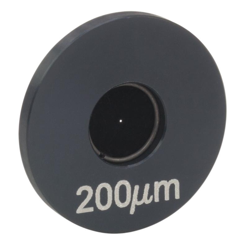
8 Method Beam Intensity Profile Circularity a M 2 Values RMS Wavefront Transmitted Power Normalized Astigmatism b Anamorphic Prism Pair 0.82 X Axis: 1.60 Y Axis: % 1.25 Scale in Microns Spatial Filter 0.93 X Axis: 1.05 Y Axis: % 0.36 Scale in Microns Circularity=d minor /d major, where d minor and d major are minor and major diameters of fitted ellipse (1/e intensity) and Circularity = 1 indicates a perfectly circular beam. Normalized astigmatism is the difference in the waist positions of the two orthogonal components of the beam, divided by the Raleigh length of the beam component with the smaller waist. Components used in each circularization system were chosen to allow the same experimental setup be used for all experiments. This had the desired effect of allowing the results of all circularization techniques to be directly compared; however, optimizing the setup for a circularization technique could have improved its performance. The mounts used for the collimating lens and the anamorphic prism pair enabled easy manipulation and integration into this experimental system. It is possible that using smaller mounts would improve results by allowing the members of each pair to be more precisely positioned with respect to one another. In addition, using made-to-order cylindrical lenses with customized focal lengths may have improved the results of the cylindrical lens pair circularization system. All results may have been affected by the use of the beam profiler software algorithm to determine the beam radii used in the circularity calculation. Hide Precision Pinholes Precision Pinholes Pinhole Diameters from 1 µm to 1 mm Pinhole Fabricated from Stainless Steel Anodized Aluminum or Black Oxide Stainless Steel Housing with 1" Outer Diameter These mounted precision pinholes are available with pinhole diameters from 1 µm to 1 mm. Each housing is engraved with the pinhole diameter, and the pinholes can be taken out of their housing by removing the retaining ring using a small tweezer or plier; use care as the pinhole is very thin. Pinholes with diameters from 5 µm to 1 mm are made of 12.7 µm thick stainless steel with a black oxide coating. Each is mounted in a Ø1", 0.10" (2.5 mm) thick stainless steel disk also coated in black oxide. Mounted Pinhole Dimensions Pinholes with diameters of 1 µm and 2 µm are made of 50.8 µm thick, stainless steel plates with a black oxide coating. They are mounted in a Ø1", 0.10" (2.5 mm) thick anodized aluminum disk that is engraved with the Item # and pinhole diameter. These 1 µm and 2 µm pinholes come with individual quailty inspections images captured using a scanning electron microscope (SEM). Item # Pinhole Diameter Diameter Tolerance Circularity Pinhole Material Housing Material P1H 1 µm / µm P2H 2 µm ±0.25 µm P5H 5 µm P10H 10 µm ±1 µm P15H 15 µm ±1.5 µm P20H 20 µm P25H 25 µm P30H 30 µm P40H 40 µm P50H 50 µm P75H 75 µm ±2 µm ±3 µm P100H 100 µm ±4 µm P150H 150 µm P200H 200 µm ±6 µm P300H 300 µm ±8 µm P400H 400 µm P500H 500 µm P600H 600 µm P700H 700 µm P800H 800 µm P900H 900 µm P1000H 1000 µm ±10 µm 85% - Stainless Steel, 50.8 µm (0.002") Thick, Black Oxide Coating Stainless Steel, 12.7 µm (0.0005") Thick, Black Oxide Coating Aluminum, Black Anodized Stainless Steel, Black Oxide Coating Rear of Mounted Pinhole Please Note: With the exception of the P1H and P2H,

9 which undergo a different manufacturing process, we are having quality issues with these pinholes that is evidenced by corrosion of the outer pinhole circumference after a period of time. Although we are rapidly working through a testing and validation process to ensure we have a stable, high-quality manufacturing process, we anticipate that the lead time on future order requests will be at least 8 weeks. Please contact Tech Support for more information. Part Number Description Price Availability P1H Ø1" Mounted Precision Pinhole, / µm Pinhole Diameter $ Today P2H Ø1" Mounted Precision Pinhole, 2 ± 0.25 µm Pinhole Diameter $ Today P5H Ø1" Mounted Precision Pinhole, 5 ± 1 µm Pinhole Diameter $74.50 Lead Time P10H Ø1" Mounted Precision Pinhole, 10 ± 1 µm Pinhole Diameter $74.50 Lead Time P15H Ø1" Mounted Precision Pinhole, 15 ± 1.5 µm Pinhole Diameter $74.50 Lead Time P20H Ø1" Mounted Precision Pinhole, 20 ± 2 µm Pinhole Diameter $67.50 Lead Time P25H Ø1" Mounted Precision Pinhole, 25 ± 2 µm Pinhole Diameter $67.50 Lead Time P30H Ø1" Mounted Precision Pinhole, 30 ± 2 µm Pinhole Diameter $67.50 Lead Time P40H Ø1" Mounted Precision Pinhole, 40 ± 3 µm Pinhole Diameter $67.50 Lead Time P50H Ø1" Mounted Precision Pinhole, 50 ± 3 µm Pinhole Diameter $67.50 Lead Time P75H Ø1" Mounted Precision Pinhole, 75 ± 3 µm Pinhole Diameter $67.50 Lead Time P100H Ø1" Mounted Precision Pinhole, 100 ± 4 µm Pinhole Diameter $67.50 Lead Time P150H Ø1" Mounted Precision Pinhole, 150 ± 6 µm Pinhole Diameter $67.50 Lead Time P200H Ø1" Mounted Precision Pinhole, 200 ± 6 µm Pinhole Diameter $67.50 Lead Time P300H Ø1" Mounted Precision Pinhole, 300 ± 8 µm Pinhole Diameter $67.50 Lead Time P400H Ø1" Mounted Precision Pinhole, 400 ± 10 µm Pinhole Diameter $67.50 Lead Time P500H Ø1" Mounted Precision Pinhole, 500 ± 10 µm Pinhole Diameter $67.50 Lead Time P600H Ø1" Mounted Precision Pinhole, 600 ± 10 µm Pinhole Diameter $67.50 Lead Time P700H Ø1" Mounted Precision Pinhole, 700 ± 10 µm Pinhole Diameter $67.50 Lead Time P800H Ø1" Mounted Precision Pinhole, 800 ± 10 µm Pinhole Diameter $67.50 Lead Time P900H Ø1" Mounted Precision Pinhole, 900 ± 10 µm Pinhole Diameter $67.50 Lead Time P1000H Ø1" Mounted Precision Pinhole, 1000 ± 10 µm Pinhole Diameter $67.50 Lead Time Hide High-Power Precision Pinholes High-Power Precision Pinholes Precision Copper Pinholes: Gold-Plated One Side Flat Poly Black (98% Emissivity) on the Reverse Side 25 µm Thickness at Aperture Black Stainless Steel Housing with 1" Outer Diameter High Damage Threshold: 5 x 10 5 W/mm 2, 75 ns 700 nm 1 x 10 6 W/mm 2, 10 ns 700 nm 10 W/mm 2, 10.6 µm Gold Surface of High- Power Mounted Pinhole Item # Pinhole Diameter Diameter Tolerance P10CH 10 µm ±1 µm P25CH 25 µm ±2 µm P50CH 50 µm ±3 µm Pinhole Thickness 25 µm (0.001") These high-power precision pinholes are designed to withstand high power densities and should be used with the beam incident on the gold-plated side. We recommend aligning the pinhole at low power, increasing the laser to full power after ensuring good throughput. Housing Material Black Stainless Steel Each pinhole is mounted in a Ø1", 0.10" (2.5 mm) thick black stainless steel disk that is engraved with the diameter of the pinhole. The pinhole can be taken out of the housing by removing the retaining ring using a small tweezer or plier; use care as the pinhole is very thin.


10 Please Note: We are having quality issues with these pinholes that is evidenced by corrosion of the outer pinhole circumference after a period of time. Although we are rapidly working through a testing and validation process to ensure we have a stable, high-quality manufacturing process, we anticipate that the lead time on future order requests will be at least 8 weeks. Please contact Tech Supportfor more information. Part Number Description Price Availability P10CH Ø1" Mounted High-Power Precision Pinhole, 10 ± 1 µm Pinhole Diameter $ Lead Time P25CH Ø1" Mounted High-Power Precision Pinhole, 25 ± 2 µm Pinhole Diameter $ Lead Time P50CH Ø1" Mounted High-Power Precision Pinhole, 50 ± 3 µm Pinhole Diameter $ Lead Time Hide Pinhole Wheels (16 Pinholes) Pinhole Wheels (16 Pinholes) Wheels with 16 Lithographically-Etched Pinholes (Transparent Glass) Pinhole Sizes from Ø25 µm to Ø2 mm Ø2.00" (Ø50.8 mm), 0.02" (0.5 mm) Thick Chrome-Plated Fused Silica Substrate Available Unmounted or with NDC-PM for Mounting (See the Assembly Tab for Mounting Instructions) AR Coated for nm on Both Sides, R avg < 0.5% These pinhole wheels are chrome-plated fused silica disks with 16 lithographically etched pinholes ranging from Ø25 µm to Ø2 mm. The radially positioned pinholes enable a user to test multiple pinhole sizes within their experiment and requires only minor alignment after each rotation. Two versions are available; the unmounted wheel itself (Item # PWH16) and a version that includes an assembly for post mounting (Item # PHWM16). Additionally, Thorlabs offers a motorized pinhole wheel (Item # MPH16) designed for confocal microscopy systems. The Ø2.00" (Ø50.8 mm), 0.02" (0.5 mm) thick disks are manufactured using photolithography; therefore, the pinholes are formed from the transparent substrate material where the chrome plating has been chemically etched away. Both sides of the wheel are AR coated [APPLIST] [APPLIST] PHWM16 Post Mounted to PY005 5-Axis Translation Stage for Alignment The inner ring is engraved with pinhole sizes and alignment marks. for nm (R avg < 0.5%) to increase transmission through the wheel. The Delrin inner disc is engraved with the pinhole sizes and alignment marks that point towards the pinholes. See the table below and the diagram above to the right for pinhole sizes and positions. The NDC-PM Post Mount Assembly (included with the PHWM16) allows the pinhole wheel to be mounted to a rotating axle that can be threaded onto any Thorlabs Ø1/2" Post. Adapters for both 8-32 and M4 mounting holes are included with each mount. The shaft of the mount can be locked by tightening the side-located setscrew using the included 0.05" (1.3 mm) hex key. Assembly of the mount is required and instructions for mounting the pinhole wheel to a NDC-PM are provided in the Assembly tab. Position a Pinhole Size Position Pinhole Size Position Pinhole Size A Ø100 µm with Ø50 µm Obstruction G Ø50 µm M Ø125 µm B Ø25 µm H Ø60 µm N Ø200 µm C Ø30 µm I Ø70 µm O Ø300 µm D Ø35 µm J Ø80 µm P Ø1000 µm E Ø40 µm K Ø90 µm Q Ø2000 µm F Ø45 µm L Ø100 µm - - Part Number Description Price Availability PHW16 16-Position Pinhole Wheel, Ø25 µm to Ø2 mm, Unmounted $ Today PHWM16 16-Position Pinhole Wheel, Ø25 µm to Ø2 mm, Mounted $ Today
11
KNIFE-EDGE RIGHT-ANGLE PRISM MIRRORS
 KNIFE-EDGE RIGHT-ANGLE PRISM MIRRORS Precision Cut Prisms Feature Bevel-Free 90 Angle Dielectric, Silver, Gold, and Aluminum Coatings Available 25 mm x 25 mm Faces Application Idea MRAK25-M01 Mounted on
30 MM CAGE CUBE MOUNTED TURNING PRISM MIRRORS
 30 MM CAGE CUBE MOUNTED TURNING PRISM MIRRORS Metallic or Dielectric Coated Turning Prism Mirrors Premounted in 30 mm Cage Cubes Compatible with SM1 Lens Tubes and 30 mm Cage System CM1 G01 4 40 Tapped
End Capped High Power Assemblies
 Fiberguide s end capped fiber optic assemblies allow the user to achieve higher coupled power into a fiber core by reducing the power density at the air/ silica interface, commonly the point of laser damage.
Laser Induced Damage Threshold of Optical Coatings
 White Paper Laser Induced Damage Threshold of Optical Coatings An IDEX Optics & Photonics White Paper Ronian Siew, PhD Craig Hanson Turan Erdogan, PhD INTRODUCTION Optical components are used in many applications
Bandpass Edge Dichroic Notch & More
 Edmund Optics BROCHURE Filters COPYRIGHT 217 EDMUND OPTICS, INC. ALL RIGHTS RESERVED 1/17 Bandpass Edge Dichroic Notch & More Contact us for a Stock or Custom Quote Today! USA: +1-856-547-3488 EUROPE:
Lithography. 3 rd. lecture: introduction. Prof. Yosi Shacham-Diamand. Fall 2004
 Lithography 3 rd lecture: introduction Prof. Yosi Shacham-Diamand Fall 2004 1 List of content Fundamental principles Characteristics parameters Exposure systems 2 Fundamental principles Aerial Image Exposure
SELECTION GUIDE MULTIPLE-ORDER QUARTZ WAVEPLATES ZERO-ORDER QUARTZ WAVEPLATES DUAL-WAVELENGTH WAVEPLATES... 85
 WAVEPLATES Mirrors Waveplates are used in applications where the control, synthesis, or analysis of the polarization state of an incident beam of light is required. Our waveplates are constructed of very
Precision Micro-Aperture Catalog
 National Aperture, Inc. Precision Micro-Aperture Catalog Version 2012 PLEASE CONTACT: Data Optics, Inc. Distributor for National Aperture, Inc. Phone: (734) 483-8228 (800) 321-9026 Fax: (734) 483-9879
Micro Precision Apertures
 National Aperture, Inc. Micro Precision Apertures Product Guide Precision apertures, targets and patterns, including round, slit, square, etc., for universal and high power applications National Aperture,
Laser Diode Mounting Kits
 Laser Diode Mounting Kits For Ø5.6mm and Ø9mm Laser Diodes Complete Mounting System with Collimating Lens If your work involves laser diodes, you ll appreciate the benefits of Optima s laser diode mounting
Laser Speckle Reducer LSR-3000 Series
 Datasheet: LSR-3000 Series Update: 06.08.2012 Copyright 2012 Optotune Laser Speckle Reducer LSR-3000 Series Speckle noise from a laser-based system is reduced by dynamically diffusing the laser beam. A
Design Description Document
 UNIVERSITY OF ROCHESTER Design Description Document Flat Output Backlit Strobe Dare Bodington, Changchen Chen, Nick Cirucci Customer: Engineers: Advisor committee: Sydor Instruments Dare Bodington, Changchen
ADVANCED OPTICS LAB -ECEN Basic Skills Lab
 ADVANCED OPTICS LAB -ECEN 5606 Basic Skills Lab Dr. Steve Cundiff and Edward McKenna, 1/15/04 Revised KW 1/15/06, 1/8/10 Revised CC and RZ 01/17/14 The goal of this lab is to provide you with practice
Using Stock Optics. ECE 5616 Curtis
 Using Stock Optics What shape to use X & Y parameters Please use achromatics Please use camera lens Please use 4F imaging systems Others things Data link Stock Optics Some comments Advantages Time and
Understanding Optical Specifications
 Understanding Optical Specifications Optics can be found virtually everywhere, from fiber optic couplings to machine vision imaging devices to cutting-edge biometric iris identification systems. Despite
PHY 431 Homework Set #5 Due Nov. 20 at the start of class
 PHY 431 Homework Set #5 Due Nov. 0 at the start of class 1) Newton s rings (10%) The radius of curvature of the convex surface of a plano-convex lens is 30 cm. The lens is placed with its convex side down
SA210-Series Scanning Fabry Perot Interferometer
 435 Route 206 P.O. Box 366 PH. 973-579-7227 Newton, NJ 07860-0366 FAX 973-300-3600 www.thorlabs.com technicalsupport@thorlabs.com SA210-Series Scanning Fabry Perot Interferometer DESCRIPTION: The SA210
MULTI-ELEMENT LENSES. Don t see exactly what you are looking for? CVI Laser Optics specializes in prototype to volume production manufacturing!
 MULTI-ELEMENT LENSES Mirrors Multi-element lenses are an ideal solution for applications requiring specialized performance and/or a high degree of aberration correction. Our line of multi-element lenses
High power VCSEL array pumped Q-switched Nd:YAG lasers
 High power array pumped Q-switched Nd:YAG lasers Yihan Xiong, Robert Van Leeuwen, Laurence S. Watkins, Jean-Francois Seurin, Guoyang Xu, Alexander Miglo, Qing Wang, and Chuni Ghosh Princeton Optronics,
StockOptics. CATALOG 2018 Europe
 StockOptics CATALOG 2018 Europe Dear asphericon customer Within the StockOptics product line, you can choose from an extensive portfolio of precision-polished aspheric lenses, cylinders and axicons. Benefit
Hamidreza Karbasi, P. Eng., PhD Conestoga College ITAL Oct. 7, 2010
 Presented at the COMSOL Conference 2010 Boston Presented by: Hamidreza Karbasi, P. Eng., PhD Conestoga College ITAL Oct. 7, 2010 Creating and Building Sustainable Environments Outline Background Objectives
Optical Isolator Tutorial (Page 1 of 2) νlh, where ν, L, and H are as defined below. ν: the Verdet Constant, a property of the
 νlh, where ν, L, and H are as defined below. ν: the Verdet Constant, a property of the") Aspheric Optical Isolator Tutorial (Page 1 of 2) Function An optical isolator is a passive magneto-optic device that only allows light to travel in one direction. Isolators are used to protect a source
Aspheric Optical Isolator Tutorial (Page 1 of 2) Function An optical isolator is a passive magneto-optic device that only allows light to travel in one direction. Isolators are used to protect a source
Tutorial Zemax 9: Physical optical modelling I
 Tutorial Zemax 9: Physical optical modelling I 2012-11-04 9 Physical optical modelling I 1 9.1 Gaussian Beams... 1 9.2 Physical Beam Propagation... 3 9.3 Polarization... 7 9.4 Polarization II... 11 9 Physical
Precision Micro-Aperture Catalog
 National Aperture, Inc. Precision Micro-Aperture Catalog Version 2013 PLEASE CONTACT: Dan Gentile Sales Associate, National Aperture, Inc. Telephone: (603) 893-7393, (800) 360-4598, Fax: (603) 893-7857
Gentec Electro-Optics, Inc
 Gentec Electro-Optics, Inc. 2013. Accessories for Beam Diagnostics Revision 1.2 2 WARRANTY The Gentec-EO accessories for beam diagnostics carry a one-year warranty (from date of shipment) against material
Gentec Electro-Optics, Inc
 Gentec Electro-Optics, Inc. 2013. Accessories for Beam Diagnostics Revision 2.0 2 WARRANTY The Gentec-EO accessories for beam diagnostics carry a one-year warranty (from date of shipment) against material
Nmark AGV-HP. High Accuracy, Thermally Stable Galvo Scanner
 Nmark AGV-HP Galvanometer Nmark AGV-HP High Accuracy, Thermally Stable Galvo Scanner Highest accuracy scanner available attains single-digit, micron-level accuracy over the field of view Optical feedback
Practical Guide to Specifying Optical Components
 Practical Guide to Specifying Optical Components OPTI 521 Introduction to Opto-Mechanical Engineering Fall 2012 December 10, 2012 Brian Parris Introduction This paper is intended to serve as a practical
k λ NA Resolution of optical systems depends on the wavelength visible light λ = 500 nm Extreme ultra-violet and soft x-ray light λ = 1-50 nm
 Resolution of optical systems depends on the wavelength visible light λ = 500 nm Spatial Resolution = k λ NA EUV and SXR microscopy can potentially resolve full-field images with 10-100x smaller features
Applying of refractive beam shapers of circular symmetry to generate non-circular shapes of homogenized laser beams
 - 1 - Applying of refractive beam shapers of circular symmetry to generate non-circular shapes of homogenized laser beams Alexander Laskin a, Vadim Laskin b a MolTech GmbH, Rudower Chaussee 29-31, 12489
The LINOS Singlets. Our quality criteria:
 The LINOS From convergent lenses and diffuse lenses to best form lenses and aspheres, our extensive selection of simple lenses, or singlets, with various focal lengths and diameters guarantees that you
R.B.V.R.R. WOMEN S COLLEGE (AUTONOMOUS) Narayanaguda, Hyderabad.
 Narayanaguda, Hyderabad.") R.B.V.R.R. WOMEN S COLLEGE (AUTONOMOUS) Narayanaguda, Hyderabad. DEPARTMENT OF PHYSICS QUESTION BANK FOR SEMESTER III PAPER III OPTICS UNIT I: 1. MATRIX METHODS IN PARAXIAL OPTICS 2. ABERATIONS UNIT II
R.B.V.R.R. WOMEN S COLLEGE (AUTONOMOUS) Narayanaguda, Hyderabad. DEPARTMENT OF PHYSICS QUESTION BANK FOR SEMESTER III PAPER III OPTICS UNIT I: 1. MATRIX METHODS IN PARAXIAL OPTICS 2. ABERATIONS UNIT II
Title: Laser marking with graded contrast micro crack inside transparent material using UV ns pulse
 Cover Page Title: Laser marking with graded contrast micro crack inside transparent material using UV ns pulse laser Authors: Futoshi MATSUI*(1,2), Masaaki ASHIHARA(1), Mitsuyasu MATSUO (1), Sakae KAWATO(2),
Nmark AGV-HP. High Accuracy, Thermally Stable Galvo Scanner
 Nmark AGV-HP High Accuracy, Thermally Stable Galvo Scanner Highest accuracy scanner available attains single-digit, micron-level accuracy over the field of view Optical feedback technology significantly
Rear Side Processing of Soda-Lime Glass Using DPSS Nanosecond Laser
 Lasers in Manufacturing Conference 215 Rear Side Processing of Soda-Lime Glass Using DPSS Nanosecond Laser Juozas Dudutis*, Paulius Gečys, Gediminas Račiukaitis Center for Physical Sciences and Technology,
Diffuser / Homogenizer - diffractive optics
 Diffuser / Homogenizer - diffractive optics Introduction Homogenizer (HM) product line can be useful in many applications requiring a well-defined beam shape with a randomly-diffused intensity profile.
Basic Optics System OS-8515C
 40 50 30 60 20 70 10 80 0 90 80 10 20 70 T 30 60 40 50 50 40 60 30 70 20 80 90 90 80 BASIC OPTICS RAY TABLE 10 0 10 70 20 60 50 40 30 Instruction Manual with Experiment Guide and Teachers Notes 012-09900B
Aspheric Lenses. Contact us for a Stock or Custom Quote Today! Edmund Optics BROCHURE
 Edmund Optics BROCHURE Aspheric Lenses products & capabilities Contact us for a Stock or Custom Quote Today! USA: +1-856-547-3488 EUROPE: +44 (0) 1904 788600 ASIA: +65 6273 6644 JAPAN: +81-3-3944-6210
MicroSpot FOCUSING OBJECTIVES
 OFR P R E C I S I O N O P T I C A L P R O D U C T S MicroSpot FOCUSING OBJECTIVES APPLICATIONS Micromachining Microlithography Laser scribing Photoablation MAJOR FEATURES For UV excimer & high-power YAG
ADVANCED OPTICS LAB -ECEN 5606
 ADVANCED OPTICS LAB -ECEN 5606 Basic Skills Lab Dr. Steve Cundiff and Edward McKenna, 1/15/04 rev KW 1/15/06, 1/8/10 The goal of this lab is to provide you with practice of some of the basic skills needed
Far field intensity distributions of an OMEGA laser beam were measured with
 Experimental Investigation of the Far Field on OMEGA with an Annular Apertured Near Field Uyen Tran Advisor: Sean P. Regan Laboratory for Laser Energetics Summer High School Research Program 200 1 Abstract
White Paper: Modifying Laser Beams No Way Around It, So Here s How
 White Paper: Modifying Laser Beams No Way Around It, So Here s How By John McCauley, Product Specialist, Ophir Photonics There are many applications for lasers in the world today with even more on the
Laser Beam Analysis Using Image Processing
 Journal of Computer Science 2 (): 09-3, 2006 ISSN 549-3636 Science Publications, 2006 Laser Beam Analysis Using Image Processing Yas A. Alsultanny Computer Science Department, Amman Arab University for
Computer Generated Holograms for Optical Testing
 Computer Generated Holograms for Optical Testing Dr. Jim Burge Associate Professor Optical Sciences and Astronomy University of Arizona jburge@optics.arizona.edu 520-621-8182 Computer Generated Holograms
Coherent Laser Measurement and Control Beam Diagnostics
 Coherent Laser Measurement and Control M 2 Propagation Analyzer Measurement and display of CW laser divergence, M 2 (or k) and astigmatism sizes 0.2 mm to 25 mm Wavelengths from 220 nm to 15 µm Determination
The Laser Processing of Diamond and Sapphire
 The Laser Processing of Diamond and Sapphire Neil Sykes Micronanics Limited neil@micronanics.com Diamond Diamond has the highest hardness and thermal conductivity of any bulk material 10/10 on the Mohs
Optical Systems. Selection Guide. Simple Telescope Kit page 6.4. Variable Attenuators for linearly polarized laser beam page 6.
 Selection Guide F-Theta Lens page 6. Compact Beam Expander page 6.3 Zoom Beam Expander page 6.3 Simple Telescope Kit page 6.4 Gauss-to-Top Hat Beam Shaping Lens page 6.5 Continuously Variable Attenuator
A novel tunable diode laser using volume holographic gratings
 A novel tunable diode laser using volume holographic gratings Christophe Moser *, Lawrence Ho and Frank Havermeyer Ondax, Inc. 85 E. Duarte Road, Monrovia, CA 9116, USA ABSTRACT We have developed a self-aligned
COLLIMATORS AND FOCUSERS RECEPTACLE STYLE
 COLLIMATORS AND FOCUSERS RECEPTACLE STYLE FEATURES: High power handling Rugged and compact design Low insertion loss Wide wavelength range 200-2100 nm Wide range of beam diameters GRIN, aspheric, achromatic,
Faraday Rotators and Isolators
 Faraday Rotators and I. Introduction The negative effects of optical feedback on laser oscillators and laser diodes have long been known. Problems include frequency instability, relaxation oscillations,
EE119 Introduction to Optical Engineering Spring 2003 Final Exam. Name:
 EE119 Introduction to Optical Engineering Spring 2003 Final Exam Name: SID: CLOSED BOOK. THREE 8 1/2 X 11 SHEETS OF NOTES, AND SCIENTIFIC POCKET CALCULATOR PERMITTED. TIME ALLOTTED: 180 MINUTES Fundamental
Will contain image distance after raytrace Will contain image height after raytrace
 Name: LASR 51 Final Exam May 29, 2002 Answer all questions. Module numbers are for guidance, some material is from class handouts. Exam ends at 8:20 pm. Ynu Raytracing The first questions refer to the
880 Quantum Electronics Optional Lab Construct A Pulsed Dye Laser
 880 Quantum Electronics Optional Lab Construct A Pulsed Dye Laser The goal of this lab is to give you experience aligning a laser and getting it to lase more-or-less from scratch. There is no write-up
EUV Plasma Source with IR Power Recycling
 1 EUV Plasma Source with IR Power Recycling Kenneth C. Johnson kjinnovation@earthlink.net 1/6/2016 (first revision) Abstract Laser power requirements for an EUV laser-produced plasma source can be reduced
Lithium Triborate (LiB 3 O 5, LBO)
") NLO Cr ys tals Introduction Lithium Triborate (LiB 3 O 5, LBO) Lithium Triborate (LiB 3 O 5 or LBO) is an excellent nonlinear optical crystal discovered and developed by FIRSM, CAS (Fujian Institute of
NLO Cr ys tals Introduction Lithium Triborate (LiB 3 O 5, LBO) Lithium Triborate (LiB 3 O 5 or LBO) is an excellent nonlinear optical crystal discovered and developed by FIRSM, CAS (Fujian Institute of
High Average Power, High Repetition Rate Side-Pumped Nd:YVO 4 Slab Laser
 High Average Power, High Repetition Rate Side-Pumped Nd:YVO Slab Laser Kevin J. Snell and Dicky Lee Q-Peak Incorporated 135 South Rd., Bedford, MA 173 (71) 75-9535 FAX (71) 75-97 e-mail: ksnell@qpeak.com,
Information & Instructions
 KEY FEATURES 1. USB 3.0 For the Fastest Transfer Rates Up to 10X faster than regular USB 2.0 connections (also USB 2.0 compatible) 2. High Resolution 4.2 MegaPixels resolution gives accurate profile measurements
Physics 431 Final Exam Examples (3:00-5:00 pm 12/16/2009) TIME ALLOTTED: 120 MINUTES Name: Signature:
 TIME ALLOTTED: 120 MINUTES Name: Signature:") Physics 431 Final Exam Examples (3:00-5:00 pm 12/16/2009) TIME ALLOTTED: 120 MINUTES Name: PID: Signature: CLOSED BOOK. TWO 8 1/2 X 11 SHEET OF NOTES (double sided is allowed), AND SCIENTIFIC POCKET CALCULATOR
Physics 431 Final Exam Examples (3:00-5:00 pm 12/16/2009) TIME ALLOTTED: 120 MINUTES Name: PID: Signature: CLOSED BOOK. TWO 8 1/2 X 11 SHEET OF NOTES (double sided is allowed), AND SCIENTIFIC POCKET CALCULATOR
Thermal Heads for Power and Single-Shot Energy - mw to KW, mj to 300J
 Thermal Heads for Power and Single-Shot Energy - mw to KW, mj to 300J The highest damage threshold in the industry Models for 1500W, 5000W and 10KW for high power laser measurement LP coating that can
EE119 Introduction to Optical Engineering Fall 2009 Final Exam. Name:
 EE119 Introduction to Optical Engineering Fall 2009 Final Exam Name: SID: CLOSED BOOK. THREE 8 1/2 X 11 SHEETS OF NOTES, AND SCIENTIFIC POCKET CALCULATOR PERMITTED. TIME ALLOTTED: 180 MINUTES Fundamental
Comparison of FRD (Focal Ratio Degradation) for Optical Fibres with Different Core Sizes By Neil Barrie
 for Optical Fibres with Different Core Sizes By Neil Barrie") Comparison of FRD (Focal Ratio Degradation) for Optical Fibres with Different Core Sizes By Neil Barrie Introduction The purpose of this experimental investigation was to determine whether there is a dependence
Comparison of FRD (Focal Ratio Degradation) for Optical Fibres with Different Core Sizes By Neil Barrie Introduction The purpose of this experimental investigation was to determine whether there is a dependence
Optical Components for Laser Applications. Günter Toesko - Laserseminar BLZ im Dezember
 Günter Toesko - Laserseminar BLZ im Dezember 2009 1 Aberrations An optical aberration is a distortion in the image formed by an optical system compared to the original. It can arise for a number of reasons
High Power Laser Delivery Assemblies COPPER FERRULE PVC COVERED SST MONOCOIL. fiberguide ANODIZED ALUMINUM HEATSINK AIRGAP TECHNOLOGY - NO EPOXY
 DESCRIPTION Multimode, step-index fibers offer a simple, efficient way to accurately deliver high power laser beams without the use of bulky, inconvenient and often heavy articulated arms. Much care has
Effects of spherical aberrations on micro welding of glass using ultra short laser pulses
 Available online at www.sciencedirect.com Physics Procedia 39 (2012 ) 563 568 LANE 2012 Effects of spherical aberrations on micro welding of glass using ultra short laser pulses Kristian Cvecek a,b,, Isamu
Chapter Ray and Wave Optics
 109 Chapter Ray and Wave Optics 1. An astronomical telescope has a large aperture to [2002] reduce spherical aberration have high resolution increase span of observation have low dispersion. 2. If two
Radial Polarization Converter With LC Driver USER MANUAL
 ARCoptix Radial Polarization Converter With LC Driver USER MANUAL Arcoptix S.A Ch. Trois-portes 18 2000 Neuchâtel Switzerland Mail: info@arcoptix.com Tel: ++41 32 731 04 66 Principle of the radial polarization
A fast F-number 10.6-micron interferometer arm for transmitted wavefront measurement of optical domes
 A fast F-number 10.6-micron interferometer arm for transmitted wavefront measurement of optical domes Doug S. Peterson, Tom E. Fenton, Teddi A. von Der Ahe * Exotic Electro-Optics, Inc., 36570 Briggs Road,
Difrotec Product & Services. Ultra high accuracy interferometry & custom optical solutions
 Difrotec Product & Services Ultra high accuracy interferometry & custom optical solutions Content 1. Overview 2. Interferometer D7 3. Benefits 4. Measurements 5. Specifications 6. Applications 7. Cases
MASSACHUSETTS INSTITUTE OF TECHNOLOGY Department of Electrical Engineering and Computer Science
 Student Name Date MASSACHUSETTS INSTITUTE OF TECHNOLOGY Department of Electrical Engineering and Computer Science 6.161 Modern Optics Project Laboratory Laboratory Exercise No. 3 Fall 2005 Diffraction
FCQ1064-APC 1064 nm 1x4 Narrowband Coupler. Mounted on
 1 X 4 SINGLE MODE FIBER OPTIC COUPLERS Wavelengths from 560 nm to 1550 nm Available 25:25:25:25 Split Ratio Terminated with 2.0 mm Narrow Key or Connectors Use for Splitting Signals FCQ1064-APC 1064 nm
Machine Vision Lyte-MV 2
 Machine Vision Lyte-MV 2 The Lyte-MV 2 Range The Lyte-MV 2 provides a reliable industrial light source for a wide range of machine vision applications including triangulation, 3D inspection and alignment.
Practical Applications of Laser Technology for Semiconductor Electronics
 Practical Applications of Laser Technology for Semiconductor Electronics MOPA Single Pass Nanosecond Laser Applications for Semiconductor / Solar / MEMS & General Manufacturing Mark Brodsky US Application
INDEX OF REFRACTION index of refraction n = c/v material index of refraction n
 INDEX OF REFRACTION The index of refraction (n) of a material is the ratio of the speed of light in vacuuo (c) to the speed of light in the material (v). n = c/v Indices of refraction for any materials
RECENTLY, using near-field scanning optical
 1 2 1 2 Theoretical and Experimental Study of Near-Field Beam Properties of High Power Laser Diodes W. D. Herzog, G. Ulu, B. B. Goldberg, and G. H. Vander Rhodes, M. S. Ünlü L. Brovelli, C. Harder Abstract
How-to guide. Working with a pre-assembled THz system
 How-to guide 15/06/2016 1 Table of contents 0. Preparation / Basics...3 1. Input beam adjustment...4 2. Working with free space antennas...5 3. Working with fiber-coupled antennas...6 4. Contact details...8
High Power Laser Delivery Assemblies COPPER FERRULE PVC COVERED SST MONOCOIL. fiberguide AIRGAP TECHNOLOGY - NO EPOXY
 DESCRIPTION Multimode, step-index fibers offer a simple, efficient way to accurately deliver high power laser beams without the use of bulky, inconvenient and often heavy articulated arms. Much care has
UV EXCIMER LASER BEAM HOMOGENIZATION FOR MICROMACHINING APPLICATIONS
 Optics and Photonics Letters Vol. 4, No. 2 (2011) 75 81 c World Scientific Publishing Company DOI: 10.1142/S1793528811000226 UV EXCIMER LASER BEAM HOMOGENIZATION FOR MICROMACHINING APPLICATIONS ANDREW
ENSC 470/894 Lab 3 Version 6.0 (Nov. 19, 2015)
") ENSC 470/894 Lab 3 Version 6.0 (Nov. 19, 2015) Purpose The purpose of the lab is (i) To measure the spot size and profile of the He-Ne laser beam and a laser pointer laser beam. (ii) To create a beam expander
ENSC 470/894 Lab 3 Version 6.0 (Nov. 19, 2015) Purpose The purpose of the lab is (i) To measure the spot size and profile of the He-Ne laser beam and a laser pointer laser beam. (ii) To create a beam expander
The below identified patent application is available for licensing. Requests for information should be addressed to:
 DEPARTMENT OF THE NAVY OFFICE OF COUNSEL NAVAL UNDERSEA WARFARE CENTER DIVISION 1176 HOWELL STREET NEWPORT Rl 0841-1708 IN REPLY REFER TO Attorney Docket No. 300048 7 February 017 The below identified
Photolithography II ( Part 2 )
") 1 Photolithography II ( Part 2 ) Chapter 14 : Semiconductor Manufacturing Technology by M. Quirk & J. Serda Saroj Kumar Patra, Department of Electronics and Telecommunication, Norwegian University of Science
1 Photolithography II ( Part 2 ) Chapter 14 : Semiconductor Manufacturing Technology by M. Quirk & J. Serda Saroj Kumar Patra, Department of Electronics and Telecommunication, Norwegian University of Science
ARCoptix. Radial Polarization Converter. Arcoptix S.A Ch. Trois-portes Neuchâtel Switzerland Mail: Tel:
 ARCoptix Radial Polarization Converter Arcoptix S.A Ch. Trois-portes 18 2000 Neuchâtel Switzerland Mail: info@arcoptix.com Tel: ++41 32 731 04 66 Radially and azimuthally polarized beams generated by Liquid
GEOMETRICAL OPTICS Practical 1. Part I. BASIC ELEMENTS AND METHODS FOR CHARACTERIZATION OF OPTICAL SYSTEMS
 GEOMETRICAL OPTICS Practical 1. Part I. BASIC ELEMENTS AND METHODS FOR CHARACTERIZATION OF OPTICAL SYSTEMS Equipment and accessories: an optical bench with a scale, an incandescent lamp, matte, a set of
BEAM SHAPING OPTICS TO IMPROVE HOLOGRAPHIC AND INTERFEROMETRIC NANOMANUFACTURING TECHNIQUES Paper N405 ABSTRACT
 BEAM SHAPING OPTICS TO IMPROVE HOLOGRAPHIC AND INTERFEROMETRIC NANOMANUFACTURING TECHNIQUES Paper N5 Alexander Laskin, Vadim Laskin AdlOptica GmbH, Rudower Chaussee 9, 89 Berlin, Germany ABSTRACT Abstract
ASPHERIC LENSES FOR OPTICS AND PHOTONICS
 ASPHERIC LENSES FOR OPTICS AND PHOTONICS Products for Laser Guides, Measurement Systems, Metrology & Bio Medical Geltech Molded Glass Aspheres Infrared Optics Fiber Collimators GRADIUM Lenses OPTICAL TECHNOLOGIES
Practical Flatness Tech Note
 Practical Flatness Tech Note Understanding Laser Dichroic Performance BrightLine laser dichroic beamsplitters set a new standard for super-resolution microscopy with λ/10 flatness per inch, P-V. We ll
POWER DETECTORS. How they work POWER DETECTORS. Overview
 G E N T E C - E O POWER DETECTORS Well established in this field for over 30 years Gentec Electro-Optics has been a leader in the field of laser power and energy measurement. The average power density
Be aware that there is no universal notation for the various quantities.
 Fourier Optics v2.4 Ray tracing is limited in its ability to describe optics because it ignores the wave properties of light. Diffraction is needed to explain image spatial resolution and contrast and
First Observation of Stimulated Coherent Transition Radiation
 SLAC 95 6913 June 1995 First Observation of Stimulated Coherent Transition Radiation Hung-chi Lihn, Pamela Kung, Chitrlada Settakorn, and Helmut Wiedemann Applied Physics Department and Stanford Linear
How to Avoid Thermal Sensor Damage & Out of Tolerance Conditions
 About Ophir-Spiricon With over 30 years of experience, the Ophir Photonics Group provides a complete line of instrumentation including power and energy meters, beam profilers, spectrum analyzers, and goniometric
Photonics West Contact us for a Stock or Custom Quote Today! Edmund Optics BROCHURE
 Edmund Optics BROHURE Photonics West 2017 Product Highlights Beam Expanders Off-xis Parabolic Mirrors Right ngle Prisms ontact us for a Stock or ustom Quote Today! US: +1-856-547-3488 EUROPE: +44 (0) 1904
plasmonic nanoblock pair
 Nanostructured potential of optical trapping using a plasmonic nanoblock pair Yoshito Tanaka, Shogo Kaneda and Keiji Sasaki* Research Institute for Electronic Science, Hokkaido University, Sapporo 1-2,
GWU versascan. Beta - Barium Borate. Optical Parametric Oscillator. User Manual
 GWU versascan Beta - Barium Borate Optical Parametric Oscillator User Manual V 1.63 Copyright GWU 03/2012 1 LASER SAFETY 4 1.1 Location of the safety labels 4 1.1.1 Label types English 7 1.1.2 Label types
attocfm I for Surface Quality Inspection NANOSCOPY APPLICATION NOTE M01 RELATED PRODUCTS G
 APPLICATION NOTE M01 attocfm I for Surface Quality Inspection Confocal microscopes work by scanning a tiny light spot on a sample and by measuring the scattered light in the illuminated volume. First,
Experimental Physics. Experiment C & D: Pulsed Laser & Dye Laser. Course: FY12. Project: The Pulsed Laser. Done by: Wael Al-Assadi & Irvin Mangwiza
 Experiment C & D: Course: FY1 The Pulsed Laser Done by: Wael Al-Assadi Mangwiza 8/1/ Wael Al Assadi Mangwiza Experiment C & D : Introduction: Course: FY1 Rev. 35. Page: of 16 1// In this experiment we
Mirrors. Plano and Spherical. Mirrors. Published on II-VI Infrared
 Page 1 of 13 Published on II-VI Infrared Plano and Spherical or total reflectors are used in laser cavities as rear reflectors and fold mirrors, and externally as beam benders in beam delivery systems.
Howie's Laser Collimator Instructions:
 Howie's Laser Collimator Instructions: WARNING: AVOID DIRECT OR MIRROR REFLECTED EYE EXPOSURE TO LASER BEAM The laser collimator is a tool that enables precise adjustment of the alignment of telescope
Beam Splitters. Diameter ET Transmission Reflectance %
 Beam Splitters Beam splitters allow a beam to be split into two beams of differing power, however, the most popular power split is 50:50 at a 45 incidence angle. The polarization needs to be considered
Optical Coherence: Recreation of the Experiment of Thompson and Wolf
 Optical Coherence: Recreation of the Experiment of Thompson and Wolf David Collins Senior project Department of Physics, California Polytechnic State University San Luis Obispo June 2010 Abstract The purpose
Novel laser power sensor improves process control
 Novel laser power sensor improves process control A dramatic technological advancement from Coherent has yielded a completely new type of fast response power detector. The high response speed is particularly
Femtosecond laser microfabrication in. Prof. Dr. Cleber R. Mendonca
 Femtosecond laser microfabrication in polymers Prof. Dr. Cleber R. Mendonca laser microfabrication focus laser beam on material s surface laser microfabrication laser microfabrication laser microfabrication