MICROSCOPIC THIN FILM METROLOGY AND VISUALIZATION
|
|
|
- Judith Allison
- 6 years ago
- Views:
Transcription
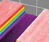
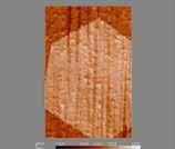
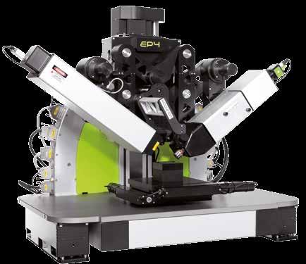
1 MICROSCOPIC THIN FILM METROLOGY AND VISUALIZATION Hex. Boron Nitride on SiO 2 MoS 2 on Sapphire Protein Spots on Glass Graphene on SiO 2 (300 nm) Si PCBM on SiO 2 Graphene on Copper Solar cell on PET Transparent substrate Black Phosphorus SAM pattern PMMA film on Si-Wafer Monolayer


2 INTRODUCTION THE MICROSCOPIC WAY OF DOING ELLIPSOMETRY This new microscopic thin film, surface and materials metrology tool generation uses a combination of auto nulling ellipsometry and microscopy to enable surface characterization with a lateral ellipsometric resolution down to 1 micron. The nanofilm_ep4 offers a variety of unique features that allow the visualization of your surface in real time. You will see in real time the structure of your sample on a microscopic scale. You can measure parameters like thickness, refractive index and absorption. You can receive maps of selected areas. You can combine the instrument with other technologies like AFM, QCM-D, reflectometry, Raman spectroscopy and many more to receive even more information from your samples. The nanofilm_ep4 is a modular instrument enabling configuration for your specific measurement tasks. The nanofilm_ep4, equipped with the standard laser can also be operated as a Brewster angle microscope, typically in LB applications UNIQUE FEATURES: Ellipsometry with the highest lateral ellipsometric resolution available on the market: Objects down to 1 micron can be resolved. This feature allows the investigation of structured samples or tiny substrates. Real time ellipsometric contrast images providing a fast view of the surface, any defects or structures. Patented region of interest (ROI) concept allows the parallel investigation of multiple areas within the selected field of view. Imaging ellipsometry in the wavelength range from 250 nm to 1700 nm provides pictures of your samples over a wide wavelength range. Continuous spectroscopic measurements allows the acquisition of an image at the selected wavelength. Knife edge illumination allows measurements on thin transparent substrates to avoid background reflection. An interesting range of accessories enable the instrument to work in a large variety of applications (SPR or solid/ liquid cells, light guides for liquid/liquid interfaces, microfluidic, temperature control, electrochemistry cells, and many more). The technology integration platform allows the adaption of various alternative measurement technologies to receive even more information from your sample. Optional single shot full field fully focused images (UltraObjektive) in the visible wavelength range allowing the easy investigation of moving samples like growing or moving SAM s, protein interaction or moving monolayers on water surfaces. Materials research example: graphene layer Bio application example: protein spots on glass
3 WHY USE ELLIPSOMETRY? WHY USE IMAGING ELLIPSOMETRY? DETECTOR LIGHT SOURCE 2D CCD (DETECTOR) MICROSCOPE OBJECTIVE POLARIZER ANALYSER POLARIZER ANALYSER COMPENSATOR SAMPLE Ellipsometry analyzes the change of polarization of light reflected from a sample and yields information about thin film layers that are often even thinner than the wavelength of the probing light itself. The change of amplitude and phase of the p and s components of the light after the reflection from the sample are depending on film properties like thickness, refractive index and absorption. Ellipsometry measures the change of the amplitudes and phases of s- and p- polarized light by rotating polarization components. The measured values are psi and delta. These values need to be put into a computer based model of the sample materials to calculate the thickness, refractive index, absorption and a variety of sample properties, including morphology, crystal quality, chemical composition or electrical conductivity. Ellipsometry is an established technology to measure multilayer film thickness, refractive index and absorption. COMPENSATOR SAMPLE Imaging ellipsometry combines microscopy and auto nulling ellipsometry. The microscopy aspect allows the direct visualization of your sample with an ellipsometric contrast image with a lateral resolution as small as 1 micron as well as the measurement of the ellipsometric parameters Delta and Psi with the highest lateral ellipsometric resolution also down to 1 micron. This enables resolving sample areas 1,000 times smaller than most micro spot equipped non-imaging spectroscopic ellipsometers. Imaging ellipsometry permits characterization of local sample parameter variation on a microscopic scale. This technology can measure the same ex-situ applications as non-imaging ellipsometers and many more. It is dedicated to applications where you have lateral structures in the range of 50 mm down to 1 micron. This includes patterned samples or where you have tiny samples like tips of a cantilever. COMPARISON NON-IMAGING AND IMAGING ELLIPSOMETERS: COMPARISON NON-IMAGING AND MAPPING ELLIPSOMETERS: The lateral ellipsometric resolution of non-imaging ellipsometers is determined by the spot size of the light source at the sample surface. Non-imaging ellipsometers reflected light from the spot guided through the analyzing system to the detection system. Spot sizes are in the range 2 mm to 35 μm. All sample structures smaller than the spot size cannot be accurately detected. The instrument will average over all structures within the sampled spot. This can provide incorrect results if your sample is not completely homogeneous. The enhanced lateral ellipsometric resolution of Imaging ellipsometry is a result of the combination of a high numerical aperture objective that images about a million sites on the illuminated sample area onto a high resolution 2 dimensional pixel detector array. This provides a resolution as small as 1 micron, depending on the wavelength of the illumination light. The first ellipsometer by Paul Drude, 1889 A mapping ellipsometer is a non-imaging ellipsometer with a motorized stage. Psi and delta readings are measured at one spot and then the table is moved to another sample loca tion and the process is repeated until enough data is collected to construct a map of the sample. The lateral resolution is determined by the spot size and the density of the sample grid. In addition to poor lateral resolution sampling time is directly related to the number of sample sites. By contrast an imaging ellipsometer can take as many as one million readings in one short exposure with vastly better lateral resolution. The images obtained are maps of Delta and Psi. Compared to a mapping ellipsometer, maps are recorded with much higher lateral ellipsometric resolution. The acquisition time for a map can be much shorter in imaging ellipsometry.


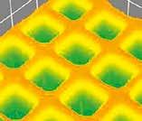
4 UNIQUE FEATURES THE HIGHEST LATERAL ELLIPSOMETRIC RESOLUTION The combination of microscopy and auto nulling ellipsometry allows a lateral ellipsometric resolution as small as 1 micron. Air SiO 2 Si Thickness map NEW FEATURE IMAGING ELLIPSOMETRY IN THE WAVELENGTH RANGE OF 250 TO 1700 NM With the use of a grating monochromator now continuous spectroscopic measurements are possible. EP4 equipped with a UV and NIR camera NEW FEATURE TECHNOLOGY INTEGRATION PLATFORM Implementation of complementary technologies e.g. Raman, AFM etc. provide even more information on your sample The new adaption platform NEW FEATURE VARIOUS UNIQUE FEATURES A variety of further new features and accessories enabling ellipsometry for new applications. EP4 beam cutter a nondestructive way to eliminate backside reflection
 Ellipsometric")


 PLEASE CONTACT US FOR YOUR")

 Knife edge illumination allows")


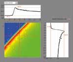
5 NEW FEATURE NEW FEATURE Air As 2 S 3 (fiber, core/clad) Ellipsometric contrast micrograph In detail: region of interest with variable shape The optional ultraobjective provides overall focused images in real time Air Graphene SiO 2 (300 nm) Si Wavelength Spectra of Delta and Psi Air Protein cantilevers Ellipsometric contrast micrograph Lambda = 280 nm Air Protein cantilevers Ellipsometric contrast micrograph Lambda = 1400 nm; (Si is transparent) PLEASE CONTACT US FOR YOUR INTEGRATION IDEAS! Integration of the Nanosurf NaniteAFM Integration of a Micro Raman System (Horiba) Knife edge illumination allows the investigation of thin transparent substrates Toluene Cetylpyridiniumbromid water Light guides enable measurements at the liquid/liquid interface tickness / nm time / min Buffer BSA gold Time dependent SPR measurements


 Imaging ellipsometry allows the real time visualization of lateral patterned SAMs of molecules with different")

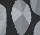
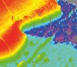
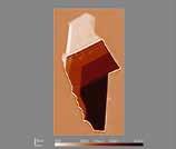
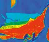
6 SELECTED APPLICATIONS GRAPHENE, 2D-MATERIALS Imaging ellipsometry allows the direct visualization of your 2D-material flakes on various substrates/materials. It is possible to measure thickness and optical properties of different 2D-material layers in the micrometer scale. Graphene SiO 2 Si 3D Psi map, lambda = 295 nm SOLAR CELLS We visualize expected and unexpected structures or non-uniformities of your material on a microscopic scale. It is possible to measure thickness, optical properties and determine band gap energies as function of location on the sample. Knife edge illumination allows the investigation of organic solar cells on transparent foils like PET foils. Air Organic layer + ZnO nanoparticles glass 3D Delta map SELF-ASSEMBLED MONOLAYER (SAM) Imaging ellipsometry allows the real time visualization of lateral patterned SAMs of molecules with different chain lengths, head groups or different packing densities. You can measure the thickness of different areas of your SAMs in parallel. Thickness differences of only 0.2 nm on different positions on your pattern can easily be detected. Air SAM pattern (OTS) SiO 2 (native) Si 3D Delta map MONOLAYER Using the unique ultraobjective allows the investigation of floating monolayers or any kind of moving or growing film with an overall focused real time image. You can see anisotropy of domain texture and structure as well as you can determine the thickness of the monolayers in the nanometer scale. The following images are showing monopalmitoyl-rac-glycerol at the air-water interface, compression speed = 180 Å 2 /min molecule. Air Monopalmitoyl-rac-glycerol water BAM image (180 Å 2 /min molecule)
 Si Thickness map")


 Si 3D")


 SiO 2")
")

 = 4.")
 = 37.")

7 Air Graphene SiO 2 (300 nm) Si Thickness map (Graphene) Air Graphene SiO 2 (300 nm) Si Thickness profile Graphene Air Graphene SiO 2 (300 nm) Si Delta map with responding Profile Air PCBM (spincoated) Si 3D Delta map Air Photoactive layer PET foil 3D Psi map (with knife edge illumination) Air PEDOT ITO PET foil 3D thickness map SAM pattern (OTS) SiO 2 (native) Si 3D thickness map SAM pattern (Hexadecanthiol+PEG-SH) gold 3D Delta map SAM pattern (Hexadecanthiol+PEG-SH) gold 3D thickness map SP (Surface pressure) = 4.2 mn/m A (Mean molecular area) = Å 2 SP = 4.4 mn/m A = 36.8 Å 2 SP = 4.4 mn/m A = 36.9 Å 2


 Si In-plane dispersion")
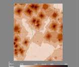
8 SELECTED APPLICATIONS PROTEIN INTERACTION Imaging ellipsometry can perform kinetic measurements of protein binding. All proteins within the field of view can be measured in parallel. Image scan of protein spots on glass VARIOUS FURTHER APPLICATIONS A wide selection of samples with structures can be visualized and measured with the unique technique of imaging ellipsometry. If you do not find your application in this overview, feel free to contact the Accurion team for specific information. Air As 2 S 3 Glass Refractive index map at 658 nm ANISOTROPIC THIN-FILMS The ep4 Mueller-Matrix upgrade offers quantitative characterization of anisotropic thin films and substrates: - refractive index and absorption for uniaxial or biaxial linear anisotropic materials - orientation of the optical axes, both in-plane and out of plane - micrographs of normalized 3x4-Mueller Matrix Air Black Phosphorus SiO 2 (300 nm) Si In-plane dispersion function BREWSTER ANGLE MICROSCOPY Brewster angle microscopy is a subset of the imaging ellipsometer. The instrument can be used to visualize monolayer at the air/water interface with typical LB accessories like troughs etc. Nanofilm_ep4 equiped with a nanofilm_ultraobjective


 water BAM")

9 Delta map protein spots Antigen/antibody interaction: Binding of polyclonal anti-rabbit IgG to immobilized Rabbit IgG DNA bar-coding of vesicles for bio chip application Air patterned As 2 S3 Glass Wavelength spectra of Delta and Psi Air patterned As 2 S 3 Glass Delta maps Air patterned As 2 S 3 Glass Psi maps Micrographs of 3x4-Müller-Matrix, normalized (m 11 = 1) Spectroscopic Mueller-Matrix measurement Orientation of optical axes obtained from Mueller-Matrix θ-scan Air Monopalmitoyl-rac-glycerol water BAM micrograph, SP 4.22 mn/m Air Ethyl stearate (monolayer) water BAM micrograph, Field-of-view ca. 600 μm Air DMPE (monolayer) water BAM micrograph during first-order phase transition

10 THE SOFTWARE IMPROVED SOFTWARE CAPABILITIES The nanofilm_ep4 software is modular. Separate software modules simplify the instrumental operation and enables parallel or offline analysis of collected data on a computer remote from the instrument. The EP4Control software manages the operation of the ep4 system. It is an interactive and easy to use control unit and automatization tool. The new AccurionServer software manages the documentation of your ep4 measurements including data from accessories and supported complementary measurement technologies. It is a sophisticated data and analysis module to enable a deeper understanding of complex systems. AccurionServer Organizes all supported data sources including accessories and optional complimentary measurement technologies and interfaces between instruments and software packages. Organizes the data storages structure (easy to use user structure). EP4Control Including image processing features: background correction (automatic), black level correction, geometric correction, signal tracking (overall brightness correction), default session storage and many more... Operating the instrument (control of moving components, taking images, performing measurements, process automization, )

.")


11 AccurionDataStudio Processing all data (images, measurement results, kinetics, structure description, etc.). Independent from the instrument and allows to analyze your data on your office PC. Special features (examples): Batch fitting: calculating delta/psi maps into thickness maps is done automatically in the background while using the instrument (pixel by pixel analysis). Images can be saved continuously also as movies with all information of the measurement parameters. New option: Pixel shot based on a stack of spectroscopic maps EP4Model Analyzing and fitting your measured data with a large selection of dispersion functions. Modeling of complex thin film systems and fitting of your measured data with the chosen model. Simulation of the fitting to follow the effect of any parameter in the model. Modelling of refractive indices (uniaxial, biaxial) and the orientation of optical axes of anisotropic materials (based on 11 elements of a normlized Mueller Matrix).


12 CONFIGURATION POSSIBILITIES CONFIGURATION POSSIBILITIES The new imaging ellipsometer nanofilm_ep4 is a modular instrument where you can select a configuration optimized for your measurement needs. TYPE Spectroscopic Imaging Ellipsometer SIE LDXe+L LIGHT SOURCE Laser Driven Xenon Lamp plus additional Laser WAVELENGTH RANGE Limited by light source/monochromator, cameras and optics EP4 CONFIGURATION WAVELENGTH RANGE ACCESSORIES FOR OPTIMUM PERFORMANCE: Laser safety cabinet support frame active vibration isolation
13 LIGHT 1 SOURCE Laser (L) 658 nm, 50 mw Xenon lamp with 44 interference filters (Xe-44IF) nm Laser driven Xenon light source (LDXe) with Grating Monochromator TECHNICAL DESCRIPTION Broadband laser for highest image quality (other laser or multi laser solutions on request) Xenon Arc lamp Filter wheel 44 interference filters, one green broadband filter, one white light position Filters Band width: 6 12 nm Laser-stabilized Xenon Arc lamp Continuous output, nm Grating Monochromator Center wavelength precision: < 1 nm includes three gratings: Grating Band width nm: 10 nm nm: 6 nm nm: 18 nm Gratings with smaller band width are available on request WHAT IS IT GOOD FOR? A laser is required for low reflective surfaces like glass or more in general low reflecting situations. Examples are insulator surfaces directly at the Brewster angle, surfaces close to the nulling conditions or close to the SPR resonance angle. You find these conditions in LB-experiments with LB films, SAMs, sub mono layers or in i-spree experiments. The 44 wavelengths enable classical ellipsometric measurements. These includes the thickness of thin transparent films ( < 1 nm and 1 μm) and materials with straight forward optical properties. The higher spectral resolution makes the detection of optical properties like band gaps, excitons or other absorption centers possible. The light source is also essential for instruments with UV- and NIR capability. The high brilliance of the light source offers in general better signal to noise ratio than a classical Xe-lamp with filter wheel. Super continuum laser (SCL) nm nm Super continuum laser Monochromatic output, no additional monochromator needed Center wavelength precision = 1 nm band width: 2 nm 450 nm 8 nm 1000 nm One benefit of a super continuum laser is the highest spectral resolution with band width down to 2 nm resulting in a higher coherent length than the other light sources, that enables additional application like the thickness determination of thicker films. Another benefit is the high brilliance that enables a better signal to noise ratio especially on smallest samples. IMAGING OPTICS TECHNICAL DESCRIPTION WHAT IS IT GOOD FOR? Focus scanner Ultraobjective (add-on, easy to exchange by customer, upgradable) New Allows realtime images at variable angles of incident (< 80 ) and is compatible with all objectives. Lateral resolution: < 1 micrometer (see chart objectives) New Scheimpflug set up for receiving an overall focused image/live video Lateral resolution: 2 micron Usable angle of incident range: The focus scanner is part of the standard ep4 detection arm. It is also used for focusing of ultraobjectives. In standard objectives, it collects focused images stripes to form an overall focused image. Focus scans take 2 5 sec, depending on the required image quality. Overall focused real time image Faster measurement; faster mapping multi spot array, improved image quality good for moving objects / kinetics (e.g. floating Monolayer on water) This is an optional exchange unit you may use in your focus scanner unit
14 CONFIGURATION POSSIBILITIES CAMERAS 1 Standard camera New NIR camera (only with NIR upgrade) TECHNICAL DESCRIPTION High quality, monochrome GigE CCD camera. Wavelength: nm pixel, 12 bits, max. 25 frames per second (fps) InGaAs FPA, cooled, GigE interface. Wavelength range: nm, pixels, 25 fps fixed WHAT IS IT GOOD FOR? Usually the CCD is used in 2 2 binning mode to improve the signal and is operated at 20 fps. For spectroscopic measurements in the NIR. This camera is added to the standard or the UV camera. Allows measurements e.g. for telecommunication materials, water absorption and many more. UV camera (only with UV upgrade) New Adaption package for second camera New Alternative cameras Back-illuminated CMOS; CameraLink interface. Wavelength: nm, pixels, 25 fps Switchable mirror or dichroic filter for camera selection (via software). Optical camera adaptation. Mechanical mounts. For spectroscopic measurements in the UV. Camera will be operated in 2 2 binning mode by default. This camera replaces the standard camera in all configurations that operate < 360 nm. The camera link interface board is included. For broad range spectroscopy a secondary camera is being used. Optics for both cameras provide a similar, position adjusted FOV. By this, seamless switching of the camera during spectral measurements is enabled. The modular software concepts allow integration of various other cameras. Especially all GenICam cameras are supported. Some cameras may require additional PC boards (camera link). OBJECTIVES FOR USE WITH 1 FOCUS SCANNER 2 objective 5 objective 10 objective 20 objective 50 objective Nanochromat New SPECIFICATION OF THE EP4, EQUIPPED WITH THE FOLLOWING OBJECTIVES: Lateral ellipsometric resolution: 10 µm FOV: 2 mm 2 mm, depends on AOI Lateral ellipsometric resolution: 4 µm FOV: 800 µm 800 µm, depends on AOI Lateral ellipsometric resolution: 2 µm FOV: 400 µm 400 µm, depends on AOI Lateral ellipsometric resolution: 1 µm FOV: 200 µm 200 µm, depends on AOI Lateral ellipsometric resolution: 1 µm* ) FOV: 70 µm 70 µm, depends on AOI Only suitable for small samples (approx mm) Lateral ellipsometric resolution: 2.5 µm FOV: 600 µm 600 µm, depends on AOI * ) lateral resolution of the microscopic image down to 0.6 µm WHAT IS IT GOOD FOR? Long distance objectives with high numerical apertures. FOV (field of view) is based on standard camera. The FOV is quadratic for this camera at 42 AOI. At different AOI, the FOV becomes rectangular depending on the angle. Resolution is defined at 400 nm. Not applicable for UV! UV/IR objective Necessary for all measurements that include wavelength between 250 and 360 nm


 Imaging Ellipsometer (IE) in PCSA")

15 ADAPTABLE TECHNOLOGIES SELECTED ACCESSORIES In situ SPR cell allowing kinetic SPR measurements Solid-liquid cells for ellipsometry at the solid liquid interface Nanofilm_ep4 with adapted Nanosurf Nanite AFM Q-Sense QCM-D E1 module integrated in the imaging ellipsometer Further adaption of technologies like Raman spectroscopy, white light interferometry, reflection spectroscopy and others are possible. PLEASE FEEL FREE TO CONTACT THE ACCURION TEAM TO DISCUSS THE ADAPTION OF A TECHNOLOGY. Light guide enables measurements at liquid/liquid interfaces and solid/ liquid interfaces at variable angles between 40 and 72 UNIQUE ACCESSORIES TECHNICAL DESCRIPTION WHAT IS IT GOOD FOR? Knife edge illumination (only combined with spectroscopic option) New Mechanic plate with a sharp edge movable into the light beam to provide an illuminated area in correspondence of the thickness of the transparent substrate. Unique feature: Allows measurements of thin transparent substrates to avoid backround reflection. Only for spectroscopic measurements. AOI measurements possible without mechanical adjustment. TECHNICAL SPECIFICATION Ellipsometer Type Open Frame-Setup Imaging Optics Motorized Goniometer Z-lift Electronics Power Supply Brewster Angle Microscope (BAM) Imaging Ellipsometer (IE) in PCSA configuration Spectroscopic Imaging Ellipsometer (SIE) in PCSA configuration Rugged aluminum frame construction with integrated multi-axis alignment. Separate electronic control unit. Automatic focus scanner for high-resolution ellipsometric contrast images and maps, 10 objective (image width 400 µm, lateral resolution 2 µm (other objectives with larger field-of-view or higher lateral resolution are available) Ultraobjective for overall focused images (optional): 2 µm lateral resolution, angle of incident range: Patented software controlled motorized goniometer Angle-of-incidence range: Angle resolution: Absolute angle accuracy: 0.01 Speed of motion: ~ 5 / sec. 10 cm travel range, 1 µm repeatability, 0.5 µm resolution Up-to-date monitor and Windows PC Embedded Linux operating system (internal only) Communication with host PC via dedicated 100 Mbit Ethernet Voltage: V ~, 50 / 60 Hz, max. current: 10 A
16 HEADQUARTER GOETTINGEN, GERMANY Accurion GmbH Stresemannstrasse Goettingen, Germany Phone: +49(0) Fax: +49(0) Web: NORTH AMERICA Accurion Inc. Inner Harbor Center 400 East Pratt Street, 8th floor Baltimore, MD Phone: Fax: Web: INDIA Accurion Scientific Instruments Pvt. Ltd. Flat 307, S.S Residency 29th Main, 2nd C Cross BTM Layout, 1 Stage, 1 Phase Bangalore , India Phone: +91(0) sharma@accurion.com Web: CHINA Accurion Scientific Instruments (Shanghai) Co. Ltd. Rm. 502, Xuhui Commercial Building, No. 168, Yude Road Xuhui District Shanghai , China Phone: +86-(0) fz@accurion.cn Web:
Your thin films visualized.
 Your thin films visualized. Graphene Graphene Protein spots on glass Graphene PCBM on SiO 2 SAM Solar cell on PET Transparent substrate Liquid/liquid interface SAM pattern PMMA film on Si-Wafer Monolayer
UVISEL. Spectroscopic Phase Modulated Ellipsometer. The Ideal Tool for Thin Film and Material Characterization
 UVISEL Spectroscopic Phase Modulated Ellipsometer The Ideal Tool for Thin Film and Material Characterization High Precision Research Spectroscopic Ellipsometer The UVISEL ellipsometer offers the best combination
_active vibration isolation desktop unit halcyonics_i4 series
 _active vibration isolation desktop unit Active Vibration Isolation Desktop Unit ABSTRACT The halcyonics_i4 is a stateof-the-art active benchtop vibration isolation system from Accurion. Aside from its
UVISEL 2. Interface. Thickness. Refractive index. Roughness. Extinction coefficient. Scientific Ellipsometric Platform
 Scientific Ellipsometric Platform The Ultimate Solution to Every Challenge in Thin Film Measurement Refractive index Interface Roughness Extinction coefficient Thickness Å to µm A Breakthrough in Thin
PhE102-VASE. PHE102 Variable Angle Spectroscopic Ellipsometer. Angstrom Advanced Inc. Angstrom Advanced. Angstrom Advanced
 Angstrom Advanced PhE102-VASE PHE102 Variable Angle Spectroscopic Ellipsometer Angstrom Advanced Instruments for Thin Film and Semiconductor Applications sales@angstromadvanced.com www.angstromadvanced.com
Thin film measurement solutions: Hardware, software, applications
 Thin film measurement solutions: Hardware, software, applications We develop and manufacture wide range of optical thin-film metrology instruments from high-precision sophisticated ellipsometry and reflectometry
M J.A. Woollam Co., Inc. Ellipsometry Solutions
 M-2000 J.A. Woollam Co., Inc. Ellipsometry Solutions Speed Discover the Difference Focused M-2000 The M-2000 line of spectroscopic ellipsometers is engineered to meet the diverse demands of thin film characterization.
attocfm I for Surface Quality Inspection NANOSCOPY APPLICATION NOTE M01 RELATED PRODUCTS G
 APPLICATION NOTE M01 attocfm I for Surface Quality Inspection Confocal microscopes work by scanning a tiny light spot on a sample and by measuring the scattered light in the illuminated volume. First,
Improving the Collection Efficiency of Raman Scattering
 PERFORMANCE Unparalleled signal-to-noise ratio with diffraction-limited spectral and imaging resolution Deep-cooled CCD with excelon sensor technology Aberration-free optical design for uniform high resolution
Bandpass Edge Dichroic Notch & More
 Edmund Optics BROCHURE Filters COPYRIGHT 217 EDMUND OPTICS, INC. ALL RIGHTS RESERVED 1/17 Bandpass Edge Dichroic Notch & More Contact us for a Stock or Custom Quote Today! USA: +1-856-547-3488 EUROPE:
Aqualog. CDOM Measurements Made Easy PARTICLE CHARACTERIZATION ELEMENTAL ANALYSIS FLUORESCENCE GRATINGS & OEM SPECTROMETERS OPTICAL COMPONENTS RAMAN
 Aqualog CDOM Measurements Made Easy ELEMENTAL ANALYSIS FLUORESCENCE GRATINGS & OEM SPECTROMETERS OPTICAL COMPONENTS PARTICLE CHARACTERIZATION RAMAN SPECTROSCOPIC ELLIPSOMETRY SPR IMAGING CDOM measurements
Measurement of Microscopic Three-dimensional Profiles with High Accuracy and Simple Operation
 238 Hitachi Review Vol. 65 (2016), No. 7 Featured Articles Measurement of Microscopic Three-dimensional Profiles with High Accuracy and Simple Operation AFM5500M Scanning Probe Microscope Satoshi Hasumura
Advanced 3D Optical Profiler using Grasshopper3 USB3 Vision camera
 Advanced 3D Optical Profiler using Grasshopper3 USB3 Vision camera Figure 1. The Zeta-20 uses the Grasshopper3 and produces true color 3D optical images with multi mode optics technology 3D optical profiling
Aqualog. Water Quality Measurements Made Easy PARTICLE CHARACTERIZATION ELEMENTAL ANALYSIS FLUORESCENCE
 Aqualog Water Quality Measurements Made Easy ELEMENTAL ANALYSIS FLUORESCENCE GRATINGS & OEM SPECTROMETERS OPTICAL COMPONENTS PARTICLE CHARACTERIZATION RAMAN SPECTROSCOPIC ELLIPSOMETRY SPR IMAGING Water
LITE /LAB /SCAN /INLINE:
 Metis Metis LITE /LAB /SCAN/ INLINE Metis LITE /LAB /SCAN /INLINE: Spectral Offline and Inline Measuring System, using Integrating Sphere, for coatings on foils/web and on large size glasses To ensure
Infrared wire grid polarizers: metrology, modeling, and laser damage threshold
 Infrared wire grid polarizers: metrology, modeling, and laser damage threshold Matthew George, Bin Wang, Jonathon Bergquist, Rumyana Petrova, Eric Gardner Moxtek Inc. Calcon 2013 Wire Grid Polarizer (WGP)
Applications of Steady-state Multichannel Spectroscopy in the Visible and NIR Spectral Region
 Feature Article JY Division I nformation Optical Spectroscopy Applications of Steady-state Multichannel Spectroscopy in the Visible and NIR Spectral Region Raymond Pini, Salvatore Atzeni Abstract Multichannel
PicoMaster 100. Unprecedented finesse in creating 3D micro structures. UV direct laser writer for maskless lithography
 UV direct laser writer for maskless lithography Unprecedented finesse in creating 3D micro structures Highest resolution in the market utilizing a 405 nm diode laser Structures as small as 300 nm 375 nm
Chemical Imaging. Whiskbroom Imaging. Staring Imaging. Pushbroom Imaging. Whiskbroom. Staring. Pushbroom
 Chemical Imaging Whiskbroom Chemical Imaging (CI) combines different technologies like optical microscopy, digital imaging and molecular spectroscopy in combination with multivariate data analysis methods.
Instructions for the Experiment
 Instructions for the Experiment Excitonic States in Atomically Thin Semiconductors 1. Introduction Alongside with electrical measurements, optical measurements are an indispensable tool for the study of
Spotlight 150 and 200 FT-IR Microscopy Systems
 S P E C I F I C A T I O N S Spotlight 150 and 200 FT-IR Microscopy Systems FT-IR Microscopy Spotlight 200 with Frontier FT-IR Spectrometer Introduction PerkinElmer Spotlight FT-IR Microscopy Systems are
attosnom I: Topography and Force Images NANOSCOPY APPLICATION NOTE M06 RELATED PRODUCTS G
 APPLICATION NOTE M06 attosnom I: Topography and Force Images Scanning near-field optical microscopy is the outstanding technique to simultaneously measure the topography and the optical contrast of a sample.
PICO MASTER 200. UV direct laser writer for maskless lithography
 PICO MASTER 200 UV direct laser writer for maskless lithography 4PICO B.V. Jan Tinbergenstraat 4b 5491 DC Sint-Oedenrode The Netherlands Tel: +31 413 490708 WWW.4PICO.NL 1. Introduction The PicoMaster
Development of a new multi-wavelength confocal surface profilometer for in-situ automatic optical inspection (AOI)
") Development of a new multi-wavelength confocal surface profilometer for in-situ automatic optical inspection (AOI) Liang-Chia Chen 1#, Chao-Nan Chen 1 and Yi-Wei Chang 1 1. Institute of Automation Technology,
Development of a new multi-wavelength confocal surface profilometer for in-situ automatic optical inspection (AOI) Liang-Chia Chen 1#, Chao-Nan Chen 1 and Yi-Wei Chang 1 1. Institute of Automation Technology,
Optical Characterization and Defect Inspection for 3D Stacked IC Technology
 Minapad 2014, May 21 22th, Grenoble; France Optical Characterization and Defect Inspection for 3D Stacked IC Technology J.Ph.Piel, G.Fresquet, S.Perrot, Y.Randle, D.Lebellego, S.Petitgrand, G.Ribette FOGALE
A simple null-field ellipsometric imaging system (NEIS) for in situ monitoring of EUV-induced deposition on EUV optics
 for in situ monitoring of EUV-induced deposition on EUV optics") A simple null-field ellipsometric imaging system (NEIS) for in situ monitoring of EUV-induced deposition on EUV optics Rashi Garg 1, Nadir Faradzhev 2, Shannon Hill 3, Lee Richter 3, P. S. Shaw 3, R. Vest
A simple null-field ellipsometric imaging system (NEIS) for in situ monitoring of EUV-induced deposition on EUV optics Rashi Garg 1, Nadir Faradzhev 2, Shannon Hill 3, Lee Richter 3, P. S. Shaw 3, R. Vest
Super High Vertical Resolution Non-Contact 3D Surface Profiler BW-S500/BW-D500 Series
 Super High Vertical Resolution Non-Contact 3D Surface Profiler BW-S500/BW-D500 Series Nikon's proprietary scanning-type optical interference measurement technology achieves 1pm* height resolution. * Height
Radial Polarization Converter With LC Driver USER MANUAL
 ARCoptix Radial Polarization Converter With LC Driver USER MANUAL Arcoptix S.A Ch. Trois-portes 18 2000 Neuchâtel Switzerland Mail: info@arcoptix.com Tel: ++41 32 731 04 66 Principle of the radial polarization
Nanonics Systems are the Only SPMs that Allow for On-line Integration with Standard MicroRaman Geometries
 Nanonics Systems are the Only SPMs that Allow for On-line Integration with Standard MicroRaman Geometries 2002 Photonics Circle of Excellence Award PLC Ltd, England, a premier provider of Raman microspectral
ECEN. Spectroscopy. Lab 8. copy. constituents HOMEWORK PR. Figure. 1. Layout of. of the
 ECEN 4606 Lab 8 Spectroscopy SUMMARY: ROBLEM 1: Pedrotti 3 12-10. In this lab, you will design, build and test an optical spectrum analyzer and use it for both absorption and emission spectroscopy. The
Bringing Answers to the Surface
 3D Bringing Answers to the Surface 1 Expanding the Boundaries of Laser Microscopy Measurements and images you can count on. Every time. LEXT OLS4100 Widely used in quality control, research, and development
Material analysis by infrared mapping: A case study using a multilayer
 Material analysis by infrared mapping: A case study using a multilayer paint sample Application Note Author Dr. Jonah Kirkwood, Dr. John Wilson and Dr. Mustafa Kansiz Agilent Technologies, Inc. Introduction
picoemerald Tunable Two-Color ps Light Source Microscopy & Spectroscopy CARS SRS
 picoemerald Tunable Two-Color ps Light Source Microscopy & Spectroscopy CARS SRS 1 picoemerald Two Colors in One Box Microscopy and Spectroscopy with a Tunable Two-Color Source CARS and SRS microscopy
Fastest high definition Raman imaging. Fastest Laser Raman Microscope RAMAN
 Fastest high definition Raman imaging Fastest Laser Raman Microscope RAMAN - 11 www.nanophoton.jp Observation A New Generation in Raman Observation RAMAN-11 developed by Nanophoton was newly created by
Micro-sensors - what happens when you make "classical" devices "small": MEMS devices and integrated bolometric IR detectors
 Micro-sensors - what happens when you make "classical" devices "small": MEMS devices and integrated bolometric IR detectors Dean P. Neikirk 1 MURI bio-ir sensors kick-off 6/16/98 Where are the targets
Dual-FL. World's Fastest Fluorometer. Measure absorbance spectra and fluorescence simultaneously FLUORESCENCE
 Dual-FL World's Fastest Fluorometer Measure absorbance spectra and fluorescence simultaneously FLUORESCENCE 100 Times Faster Data Collection The only simultaneous absorbance and fluorescence system available
Electrical Characterization
 Listing and specification of characterization equipment at ISC Konstanz 30.05.2016 Electrical Characterization µw-pcd (Semilab) PV2000 (Semilab) - spatially resolved minority charge carrier lifetime -diffusion
Lithography. 3 rd. lecture: introduction. Prof. Yosi Shacham-Diamand. Fall 2004
 Lithography 3 rd lecture: introduction Prof. Yosi Shacham-Diamand Fall 2004 1 List of content Fundamental principles Characteristics parameters Exposure systems 2 Fundamental principles Aerial Image Exposure
A Laser-Based Thin-Film Growth Monitor
 TECHNOLOGY by Charles Taylor, Darryl Barlett, Eric Chason, and Jerry Floro A Laser-Based Thin-Film Growth Monitor The Multi-beam Optical Sensor (MOS) was developed jointly by k-space Associates (Ann Arbor,
MEMS for RF, Micro Optics and Scanning Probe Nanotechnology Applications
 MEMS for RF, Micro Optics and Scanning Probe Nanotechnology Applications Part I: RF Applications Introductions and Motivations What are RF MEMS? Example Devices RFIC RFIC consists of Active components
Practical work no. 3: Confocal Live Cell Microscopy
 Practical work no. 3: Confocal Live Cell Microscopy Course Instructor: Mikko Liljeström (MIU) 1 Background Confocal microscopy: The main idea behind confocality is that it suppresses the signal outside
Add CLUE to your SEM. High-efficiency CL signal-collection. Designed for your SEM and application. Maintains original SEM functionality
 Add CLUE to your SEM Designed for your SEM and application The CLUE family offers dedicated CL systems for imaging and spectroscopic analysis suitable for most SEMs. In addition, when combined with other
Nikon Instruments Europe
 Nikon Instruments Europe Recommendations for N-SIM sample preparation and image reconstruction Dear customer, We hope you find the following guidelines useful in order to get the best performance out of
Absentee layer. A layer of dielectric material, transparent in the transmission region of
 Glossary of Terms A Absentee layer. A layer of dielectric material, transparent in the transmission region of the filter, due to a phase thickness of 180. Absorption curve, absorption spectrum. The relative
EE119 Introduction to Optical Engineering Spring 2003 Final Exam. Name:
 EE119 Introduction to Optical Engineering Spring 2003 Final Exam Name: SID: CLOSED BOOK. THREE 8 1/2 X 11 SHEETS OF NOTES, AND SCIENTIFIC POCKET CALCULATOR PERMITTED. TIME ALLOTTED: 180 MINUTES Fundamental
Microscopic Structures
 Microscopic Structures Image Analysis Metal, 3D Image (Red-Green) The microscopic methods range from dark field / bright field microscopy through polarisation- and inverse microscopy to techniques like
The only simultaneous absorbance and f uorescence system for water quality analysis! Aqualog
 The only simultaneous absorbance and fluorescence system for water quality analysis! Aqualog CDOM measurements made easy. The only simultaneous absorbance and fluorescence system for water quality analysis!
Performance Comparison of Spectrometers Featuring On-Axis and Off-Axis Grating Rotation
 Performance Comparison of Spectrometers Featuring On-Axis and Off-Axis Rotation By: Michael Case and Roy Grayzel, Acton Research Corporation Introduction The majority of modern spectrographs and scanning
SpectraPro 2150 Monochromators and Spectrographs
 SpectraPro 215 Monochromators and Spectrographs SpectraPro 215 15 mm imaging spectrographs and monochromators from are the industry standard for researchers who demand the highest quality data. Acton monochromators
Fast Laser Raman Microscope RAMAN
 Fast Laser Raman Microscope RAMAN - 11 www.nanophoton.jp Fast Raman Imaging A New Generation of Raman Microscope RAMAN-11 developed by Nanophoton was created by combining confocal laser microscope technology
Park NX-Hivac The world s most accurate and easy to use high vacuum AFM for failure analysis.
 Park NX-Hivac The world s most accurate and easy to use high vacuum AFM for failure analysis www.parkafm.com Park NX-Hivac High vacuum scanning for failure analysis applications 4 x 07 / Cm3 Current (µa)
Laser Speckle Reducer LSR-3000 Series
 Datasheet: LSR-3000 Series Update: 06.08.2012 Copyright 2012 Optotune Laser Speckle Reducer LSR-3000 Series Speckle noise from a laser-based system is reduced by dynamically diffusing the laser beam. A
Specifications. Offers the best spatial resolution for multi-stripe spectroscopy. Provides the user the choice of either high accuracy slit mechanism
 SpectraPro Series Monochromators and Spectrographs The PI/Acton SpectraPro Series imaging spectrographs and monochromators represent the latest advance in the industry-standard SpectraPro family. The SpectraPro
CONFIGURING. Your Spectroscopy System For PEAK PERFORMANCE. A guide to selecting the best Spectrometers, Sources, and Detectors for your application
 CONFIGURING Your Spectroscopy System For PEAK PERFORMANCE A guide to selecting the best Spectrometers, s, and s for your application Spectral Measurement System Spectral Measurement System Spectrograph
QE65000 Spectrometer. Scientific-Grade Spectroscopy in a Small Footprint. now with. Spectrometers
 QE65000 Spectrometer Scientific-Grade Spectroscopy in a Small Footprint QE65000 The QE65000 Spectrometer is the most sensitive spectrometer we ve developed. Its Hamamatsu FFT-CCD detector provides 90%
WITec Alpha 300R Quick Operation Summary October 2018
 WITec Alpha 300R Quick Operation Summary October 2018 This document is frequently updated if you feel information should be added, please indicate that to the facility manager (currently Philip Carubia,
Multispectral. imaging device. ADVANCED LIGHT ANALYSIS by. Most accurate homogeneity MeasureMent of spectral radiance. UMasterMS1 & UMasterMS2
 Multispectral imaging device Most accurate homogeneity MeasureMent of spectral radiance UMasterMS1 & UMasterMS2 ADVANCED LIGHT ANALYSIS by UMaster Ms Multispectral Imaging Device UMaster MS Description
INDIAN INSTITUTE OF TECHNOLOGY BOMBAY
 IIT Bombay requests quotations for a high frequency conducting-atomic Force Microscope (c-afm) instrument to be set up as a Central Facility for a wide range of experimental requirements. The instrument
Horiba LabRAM ARAMIS Raman Spectrometer Revision /28/2016 Page 1 of 11. Horiba Jobin-Yvon LabRAM Aramis - Raman Spectrometer
 Page 1 of 11 Horiba Jobin-Yvon LabRAM Aramis - Raman Spectrometer The Aramis Raman system is a software selectable multi-wavelength Raman system with mapping capabilities with a 400mm monochromator and
Fast Laser Raman Microscope RAMAN
 Fast Laser Raman Microscope RAMAN - 11 www.nanophoton.jp Fast Raman Imaging A New Generation of Raman Microscope RAMAN-11 developed by Nanophoton was created by combining confocal laser microscope technology
Aqualog. Water Quality Measurements Made Easy FLUORESCENCE
 Aqualog Water Quality Measurements Made Easy FLUORESCENCE Water quality measurements made easy The only simultaneous absorbance and fluorescence system for water quality analysis! The new Aqualog is the
Säntis 300 Full wafer cathodoluminescence control up to 300 mm diameter
 Säntis 300 Full wafer cathodoluminescence control up to 300 mm diameter Overview The Säntis 300 system has been designed for fully automated control of 150, 200 and 300 mm wafers. Attolight s Quantitative
Optical In-line Control of Web Coating Processes
 AIMCAL Europe 2012 Peter Lamparter Web Coating Conference Carl Zeiss MicroImaging GmbH 11-13 June / Prague, Czech Republic Carl-Zeiss-Promenade 10 07745 Jena, Germany p.lamparter@zeiss.de +49 3641 642221
Applications of Optics
 Nicholas J. Giordano www.cengage.com/physics/giordano Chapter 26 Applications of Optics Marilyn Akins, PhD Broome Community College Applications of Optics Many devices are based on the principles of optics
Section 2: Lithography. Jaeger Chapter 2 Litho Reader. The lithographic process
 Section 2: Lithography Jaeger Chapter 2 Litho Reader The lithographic process Photolithographic Process (a) (b) (c) (d) (e) (f) (g) Substrate covered with silicon dioxide barrier layer Positive photoresist
HR2000+ Spectrometer. User-Configured for Flexibility. now with. Spectrometers
 Spectrometers HR2000+ Spectrometer User-Configured for Flexibility HR2000+ One of our most popular items, the HR2000+ Spectrometer features a high-resolution optical bench, a powerful 2-MHz analog-to-digital
Difrotec Product & Services. Ultra high accuracy interferometry & custom optical solutions
 Difrotec Product & Services Ultra high accuracy interferometry & custom optical solutions Content 1. Overview 2. Interferometer D7 3. Benefits 4. Measurements 5. Specifications 6. Applications 7. Cases
Repair System for Sixth and Seventh Generation LCD Color Filters
 NTN TECHNICAL REVIEW No.722004 New Product Repair System for Sixth and Seventh Generation LCD Color Filters Akihiro YAMANAKA Akira MATSUSHIMA NTN's color filter repair system fixes defects in color filters,
:... resolution is about 1.4 μm, assumed an excitation wavelength of 633 nm and a numerical aperture of 0.65 at 633 nm.
 PAGE 30 & 2008 2007 PRODUCT CATALOG Confocal Microscopy - CFM fundamentals :... Over the years, confocal microscopy has become the method of choice for obtaining clear, three-dimensional optical images
Cutting-edge Atomic Force Microscopy techniques for large and multiple samples
 Cutting-edge Atomic Force Microscopy techniques for large and multiple samples Study of up to 200 mm samples using the widest set of AFM modes Industrial standards of automation A unique combination of
Section 2: Lithography. Jaeger Chapter 2 Litho Reader. EE143 Ali Javey Slide 5-1
 Section 2: Lithography Jaeger Chapter 2 Litho Reader EE143 Ali Javey Slide 5-1 The lithographic process EE143 Ali Javey Slide 5-2 Photolithographic Process (a) (b) (c) (d) (e) (f) (g) Substrate covered
Minimizes reflection losses from UV-IR; Optional AR coatings & wedge windows are available.
 Now Powered by LightField PyLoN:2K 2048 x 512 The PyLoN :2K is a controllerless, cryogenically-cooled CCD camera designed for quantitative scientific spectroscopy applications demanding the highest possible
Spectral phase shaping for high resolution CARS spectroscopy around 3000 cm 1
 Spectral phase shaping for high resolution CARS spectroscopy around 3 cm A.C.W. van Rhijn, S. Postma, J.P. Korterik, J.L. Herek, and H.L. Offerhaus Mesa + Research Institute for Nanotechnology, University
Sensors and Metrology - 2 Optical Microscopy and Overlay Measurements
 Sensors and Metrology - 2 Optical Microscopy and Overlay Measurements 1 Optical Metrology Optical Microscopy What is its place in IC production? What are the limitations and the hopes? The issue of Alignment
MS260i 1/4 M IMAGING SPECTROGRAPHS
 MS260i 1/4 M IMAGING SPECTROGRAPHS ENTRANCE EXIT MS260i Spectrograph with 3 Track Fiber on input and InstaSpec IV CCD on output. Fig. 1 OPTICAL CONFIGURATION High resolution Up to three gratings, with
SOLAR CELL INSPECTION WITH RAPTOR PHOTONICS OWL (SWIR) AND FALCON (EMCCD)
 AND FALCON (EMCCD)") Technical Note Solar Cell Inspection SOLAR CELL INSPECTION WITH RAPTOR PHOTONICS OWL (SWIR) AND FALCON (EMCCD) August 2012, Northern Ireland Solar cell inspection relies on imaging the photoluminescence
Technical Note Solar Cell Inspection SOLAR CELL INSPECTION WITH RAPTOR PHOTONICS OWL (SWIR) AND FALCON (EMCCD) August 2012, Northern Ireland Solar cell inspection relies on imaging the photoluminescence
7 CHAPTER 7: REFRACTIVE INDEX MEASUREMENTS WITH COMMON PATH PHASE SENSITIVE FDOCT SETUP
 7 CHAPTER 7: REFRACTIVE INDEX MEASUREMENTS WITH COMMON PATH PHASE SENSITIVE FDOCT SETUP Abstract: In this chapter we describe the use of a common path phase sensitive FDOCT set up. The phase measurements
ARCoptix. Radial Polarization Converter. Arcoptix S.A Ch. Trois-portes Neuchâtel Switzerland Mail: Tel:
 ARCoptix Radial Polarization Converter Arcoptix S.A Ch. Trois-portes 18 2000 Neuchâtel Switzerland Mail: info@arcoptix.com Tel: ++41 32 731 04 66 Radially and azimuthally polarized beams generated by Liquid
Dynamic Phase-Shifting Microscopy Tracks Living Cells
 from photonics.com: 04/01/2012 http://www.photonics.com/article.aspx?aid=50654 Dynamic Phase-Shifting Microscopy Tracks Living Cells Dr. Katherine Creath, Goldie Goldstein and Mike Zecchino, 4D Technology
Lecture 04: Solar Imaging Instruments
 Hale COLLAGE (NJIT Phys-780) Topics in Solar Observation Techniques Lecture 04: Solar Imaging Instruments Wenda Cao New Jersey Institute of Technology Valentin M. Pillet National Solar Observatory SDO
Nanosurf easyscan 2 FlexAFM
 Nanosurf easyscan 2 FlexAFM Your Versatile AFM System for Materials and Life Science www.nanosurf.com The new Nanosurf easyscan 2 FlexAFM scan head makes measurements in liquid as simple as measuring in
Introduction of New Products
 Field Emission Electron Microscope JEM-3100F For evaluation of materials in the fields of nanoscience and nanomaterials science, TEM is required to provide resolution and analytical capabilities that can
Section 2: Lithography. Jaeger Chapter 2. EE143 Ali Javey Slide 5-1
 Section 2: Lithography Jaeger Chapter 2 EE143 Ali Javey Slide 5-1 The lithographic process EE143 Ali Javey Slide 5-2 Photolithographic Process (a) (b) (c) (d) (e) (f) (g) Substrate covered with silicon
TECHNICAL QUICK REFERENCE GUIDE MANUFACTURING CAPABILITIES GLASS PROPERTIES COATING CURVES REFERENCE MATERIALS
 TECHNICAL QUICK REFERENCE GUIDE COATING CURVES GLASS PROPERTIES MANUFACTURING CAPABILITIES REFERENCE MATERIALS TABLE OF CONTENTS Why Edmund Optics?... 3 Anti-Reflective (AR) Coatings... 4-16 Metallic Mirror
NSOM (SNOM) Overview
 Overview") NSOM (SNOM) Overview The limits of far field imaging In the early 1870s, Ernst Abbe formulated a rigorous criterion for being able to resolve two objects in a light microscope: d > ë / (2sinè) where d
NSOM (SNOM) Overview The limits of far field imaging In the early 1870s, Ernst Abbe formulated a rigorous criterion for being able to resolve two objects in a light microscope: d > ë / (2sinè) where d
Module - 2 Lecture - 13 Lithography I
 Nano Structured Materials-Synthesis, Properties, Self Assembly and Applications Prof. Ashok. K.Ganguli Department of Chemistry Indian Institute of Technology, Delhi Module - 2 Lecture - 13 Lithography
Oriel MS260i TM 1/4 m Imaging Spectrograph
 Oriel MS260i TM 1/4 m Imaging Spectrograph MS260i Spectrograph with 3 Track Fiber on input and InstaSpec CCD on output. The MS260i 1 4 m Imaging Spectrographs are economical, fully automated, multi-grating
Supplementary Materials for
 advances.sciencemag.org/cgi/content/full/4/2/e1700324/dc1 Supplementary Materials for Photocarrier generation from interlayer charge-transfer transitions in WS2-graphene heterostructures Long Yuan, Ting-Fung
Spectro p photomete p r V-700 series
 Spectrophotometer p V-700 series V-700 Series UV-Vis/NIR Spectrophotometers V-730 SBW=1.0 nm Class-leading high S/N V-730BIO New irm & Spectra Manager V-750/760/770 Wavelength-independent dynamic range
Photonics and Optical Communication
 Photonics and Optical Communication (Course Number 300352) Spring 2007 Dr. Dietmar Knipp Assistant Professor of Electrical Engineering http://www.faculty.iu-bremen.de/dknipp/ 1 Photonics and Optical Communication
Tunable KiloArc. Tunable Broadband Light Source.
 Optical Building Blocks Corporation Tunable KiloArc Tunable Broadband Light Source www.obb1.com Tunable KiloArc Need a CW laser that is tunable from 250 to 1,100 nm? yes Need it to deliver Hundreds of
Coherent Laser Measurement and Control Beam Diagnostics
 Coherent Laser Measurement and Control M 2 Propagation Analyzer Measurement and display of CW laser divergence, M 2 (or k) and astigmatism sizes 0.2 mm to 25 mm Wavelengths from 220 nm to 15 µm Determination
Research Grade Xenon Arc Lamp Sources LH-Series 75 W - 300W
 Research Grade Xenon Arc Lamp Sources LH-Series 75 W - 300W Features Vertical or horizontal bulb and housing operation Xenon arc lamps from 75W to 300W Multiple collimated or focused output optics in various
Will contain image distance after raytrace Will contain image height after raytrace
 Name: LASR 51 Final Exam May 29, 2002 Answer all questions. Module numbers are for guidance, some material is from class handouts. Exam ends at 8:20 pm. Ynu Raytracing The first questions refer to the
Spectroscopy in the UV and Visible: Instrumentation. Spectroscopy in the UV and Visible: Instrumentation
 Spectroscopy in the UV and Visible: Instrumentation Typical UV-VIS instrument 1 Source - Disperser Sample (Blank) Detector Readout Monitor the relative response of the sample signal to the blank Transmittance
III III 0 IIOI DID IIO 1101 I II 0II II 100 III IID II DI II
 (19) United States III III 0 IIOI DID IIO 1101 I0 1101 0II 0II II 100 III IID II DI II US 200902 19549A1 (12) Patent Application Publication (10) Pub. No.: US 2009/0219549 Al Nishizaka et al. (43) Pub.
Integrated disruptive components for 2µm fibre Lasers ISLA. 2 µm Sub-Picosecond Fiber Lasers
 Integrated disruptive components for 2µm fibre Lasers ISLA 2 µm Sub-Picosecond Fiber Lasers Advantages: 2 - microns wavelength offers eye-safety potentially higher pulse energy and average power in single
SUPPLEMENTARY INFORMATION
 Optically reconfigurable metasurfaces and photonic devices based on phase change materials S1: Schematic diagram of the experimental setup. A Ti-Sapphire femtosecond laser (Coherent Chameleon Vision S)
Advanced Research Raman System Raman Spectroscopy Systems
 T600 Advanced Research Raman System Raman Spectroscopy Systems T600 Advanced Research Raman System T600 Triple stage Raman Spectrometer: The only solution for unprecedented stability and performance! Robust
Products - Microarray Scanners - Laser Scanners - InnoScan 900 Series and MAPIX Software
 Products - Microarray Scanners - Laser Scanners - InnoScan 900 Series and MAPIX Software Arrayit offers the world s only next generation microarray scanning technology, with proprietary rotary motion control,