Visible Light Photon R&D in the US. A. Bross KEK ISS Meeting January 25, 2006
|
|
|
- Margery Reeves
- 5 years ago
- Views:
Transcription
1 Visible Light Photon R&D in the US A. Bross KEK ISS Meeting January 25, 2006
2 Some History First
3 VLPC History In 1987, a paper was published by Rockwell detailing the performance of Solid State PhotoMultipliers (SSPMs). These solid state devices detected both visible and infrared light. Infrared detection technology is regulated under international treaty so Fermilab proposed a device which maintained the visible light response, but reduced the infrared response. This device is called a Visible Light Photon Counter (VLPC). With the successful demonstration of VLPC technology, the High-Resolution Scintillating Fiber Tracking Experiment (HiSTE) proposal detailed using scintillating fiber technology combined with VLPCs to track particles from high energy particle collisions. There have been six models of HiSTE chips, with HiSTE-VI being used in the DØ experiment.
4 VLPC Operational Principles Photon is converted the intrinsic region, creating an electron-hole pair. Hole drifts into the drift region, where it knocks an electron out from an atom. Electron accelerates back through gain region, knocking electrons from atoms as it goes. Spacer region and substrate are for mechanical support and field shaping. Thus each photon generates a pulse of many electrons. Gains of 20,000 60,000 are achievable. Photon Intrinsic Region + e Top Contact (+) Gain Region h E field Undoped Silicon (Blocking) Layer Gain Region Drift Region Drift Region D + flow Doped Silicon Layer Substrate Spacer Region - Bottom Contact (-)
5 VLPC Timeline Initial SSPM Publication Fermilab Approaches Rockwell About HEP Applications VLPCs Differentiated From SSPMs HiSTE Proposal Submitted HiSTE IV Manufactured 3000 Channel Scintillating Fiber Test at Fermilab Large Scale Testing of HiSTE VI Begins 140,000 VLPC Pixels DØ Data Taking Commences The Hunt Is On!! Experiments By Rockwell And Fermilab/UCLA Using Scintillating Fibers and SSPMs VLPCs Successfully Demonstrated HiSTE I, HiSTE II, HiSTE III DØ Scintillating Fiber Tracker Proposed HiSTE VI Wafers Grown Final VLPC Design DØ Scintillating Fiber Tracker Installed Commissioning Begins
")

6 HiSTE VI Solid state photon detectors Operate at a few degrees Kelvin (~ F) Bias voltage 6-8 Volts Detects single photons Can work in a high rate environment Visible
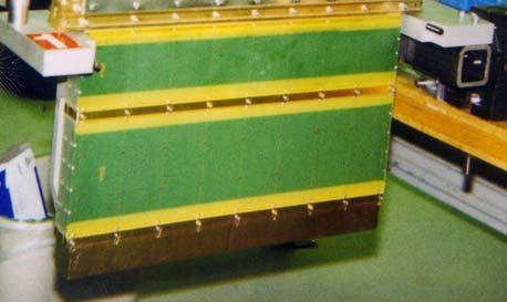
7 DØ Scintillating Fiber Tracker: Charged particles cross a scintillating fiber, where it causes a blink of light. Operational Principles The light is transported via optical fiber over a distance of 8-11 meters to a device called a VLPC which converts light into electricity. VLPC are solid state devices which run at cryogenic temperatures. A cassette of VLPC devices contains 1024 channels and is housed in a cryostat, which carefully regulates the operating temperature. Mirror Scintillating Fiber Photodetector Cassette Cryostat Optical Connector Waveguide Fiber Electrical Signal Out
8 VLPC History The Visible light Photon Counter is an impurity band avalanche photodiode that operates in the range of 6-10K Parameters (from D0 program) QE = 85% Gain = 35k-65k Noise = khz (@1 pe threshold) Most-Importantly: COST For the D0 program (approximately 120k pixels (1mm) the per channel cost for the VLPC system (packaged, tested, delivered) was $60/Ch
9 Silicon Wafer Processing Conventional silicon processing at >µm resolution 3-inch wafers for D0 176 VLPC arrays 1408 VLPCs Future production 6-inch wafers About 5000 to VLPCs/wafer Array format(s) TBD
10 VLPC Hybrid A B A Face photo of assembled hybrid C A B A = VLPC die B = AlN substrate B Edge view of assembled hybrid C = Indium solder preform
11 Uniformity Issue
12 Hybrid Assembly Process Holes for weights Top View Bottom Boat Substrate Holder Dice Holder Top Boat Weights Top Boat Side View Dice Holder Bottom Boat Substrate Holder Vacuum Sealer
13 Improved Gain Uniformity Number of VLPCs Gain (10 3 electrons/photon) D0 VLPC gain varied by material group (~20 wafers) Smaller variations across wafers and from wafer to wafer Causes: ca 1980 growth reactors with insufficient control of gas flows/growth temperature Multi-wafer growth geometry Solution for D0: Sort Solution for next generation: Utilization of modern,


14

15
16 New R&D
17 HISTE VII Lawrence Semiconductor Research Laboratory (LSRL) won Phase I SBIR to develop new VLPC material Boeing DRS Technologies consulted Henry Hogue/Dutch Stapelbroek Reactors at Boeing/DRS decommissioned after D0 work Since then LSRL has been growing BIB epi material for all of DRS s projects EKV Star Wars Lite Phase I objectives Reproduce HISTE VI and SSPM material Scan target parameters with various splits Measure bulk properties Spreading Resistance Profile Cryo C-V 4 Point probe FTIR infrared spectroscopy Defect density Goal Better Uniformity (gain) and lower defect density
18 HISTE VII 80 5 wafers were grown Note: LSRL reactors can go up to 8 Limited to 6 by processing at DRS Used 5 followed BIB work 8 Splits of 10 wafers each Note: based on HISTE VI geometry this represents 300k potential pixels Used highly doped (As) substrates in order to go to large wafer size D0 used antimony Layer IV (undoped) L ay er III (A s an d B ) L ayer II (A s an d B ) Layer I (A s and B ) H ighly doped substrate (A s)
19 HISTE VII Spreading Resistance Profiling (SRP) Determines layer thicknesses and Ar concentration in doped layers Four point probe (4PP) and Fourier transform Infrared Spectroscopy Sheet resistance and thickness Single layer Cryogenic C-V Characterize acceptor background and boron doping levels in gain region. T L C R Samples taken from select group of wafers (8X5) for analysis B flat
20 HISTE VII FTIR and 4PP Results Uniformity 5 to 10X more uniform than D0 material Target thickness 18 µm
21 HISTE VII SRP results V L P C S p r e a d i n g R e s i s t a n c e P r o f i l e - S a m p l e J E E E E L a y e r 4 L a y e r 3 L a y e r 2 L a y e r E E Concentration (at/cc) T o p C e n t e r B o t t o m L e f t R i g h t S p e c S u b s t r a t e E E E T h i c k n e s s ( m i c r o n s ) Target As concentrations: Layers 1&2: 9X10 17 cm X10 17 cm -3 for layer 3
22 HISTE VII Cryo C-V Measures Boron doping in gain region Average: 3.0X10 13 cm -3 Target 3.5X10 13 cm -3 16% low. RMS 12% consistent with measurement precision

23 HISTE VII Epitaxial layer defects Scanned with bright light inspection and verified with microscope Average defect count less than 5 per 5 wafer Corresponds to 0.08 defects per cm 2 D0 material: 4 defects per cm 2 X50! VLPC Pulses? Since processing was not part of Phase I HH made detector from epi using In contacts Saw pulses
24 HISTE VII Phase II ($750k) Fabricate and test detectors using the epitaxial layers grown in Phase I. Refine the detector design based on the test results, and revise the epitaxial layer specifications accordingly. Grow a second round of epitaxial layers. Extend the design work to include an integrated package. Fabricate, test and package detectors in a form that will be offered for sale in sample quantities to end users. Iterate the design, growth and packaging into a successful commercial product. So we can expect Packaged devices (HISTE VI geometry) HISTE VI, VII, VIII? + SSPM High Density geometry will likely be tried also 16 X mm pixel? Potential for many pixels
25 Improvements to VLPC Wafer Processing AR Coating D0 VLPCs used quarter wave SiO 2 AR coating 5-10% reflection loss Silicon nitride and silicon monoxide are better matched coating materials now available Should improve VLPC QE from ~85% to >90% Scratch Coating D0 VLPCs had exposed AL traces Resulted in minor die losses due to handling Over coating traces will eliminate this loss
26 Process Lot split Lot started with two 5 wafers from each of 8 epitaxy groups grown by LSRL in SBIR Ph 1 Plus 2 wafers each of 7 old 3 VLPC epitaxy groups grown after DZERO product runs Plan: Process 1 wafer of each type through standard process and evaluate Dice, package (not hybrids), and performance test at DRS Based on test results, provide epitaxy parameters to LSRL for new material run on SBIR Put remaining wafers through improved AR coating process Etch oxide from detector area Apply silicon nitride AR coating thickness over entire wafer Improved AR coat plus scratch coat over aluminum leads Open coating for gold deposition on pads as before Prepare hybrids from best epitaxy groups for testing at Fermilab
 4X8 (.")
 [D0] 1")

27 3 X 3 (3mm X 3mm) 4X8 (.5mm) 2X4 (1 mm) [D0] 1 cm 2 single pixel 16X16 (.5mm)
 Mask")
28 32 Channel array (.5 mm pixel) Mask Design
 Mask")
29 16 X 16 (.5 mm pixel) Mask Design


30 R&D production Devices SiN AR coating Expect QE 98%
31 HISTE VII Conclusions on SBIR R&D Program Phase I and II work went very well LSRL is a very competent/professional organization Grew 80 wafers can be fabricated for about $150k! This is the epitaxial growth step: $0.1/1 mm pixel Note D0 cost was $2/pixel We estimate that the epitaxial wafers can be processed for about $2-3k/wafer About $0.3/1 mm pixel We expect yields of 90% (to be determined in upcoming tests) D0 Yield was 70% New material is 5 to 10X more uniform than the D0 material and the defect density is 50X smaller 1 mm pixel cost at wafer level <$0.5/pixel!
32 Next Steps Integration/packaging Cryo This represented about ½ the cost in D0 ($25/pixel) Going to larger array and 0.5 mm pixel improves this situation tremendously This R&D has not started, no funding in sight presently Going to 16 X mm pixel array See over a factor 10 reduction in cost in packaging Expensive for D0 Convention LHe plant MICE has made progress Developed system using commercial cryo-coolers Tested at Fermilab and KEK Has worked extremely well

33 VLPC Readout System Using 1024 channel D0 VLPC cassette design 8-1mm element array However, will use a cryocooler system to reach 9K operating temperature Sumitomo SRDK-451D


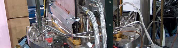


34 MICE VLPC Cryo-System The new system has been built, commissioned, and now operated for a period of 2 months at Fermilab and 3 months in Japan

35 Cryo Operation System Stability has been impressive! ± 10 mk over a period of months Just running cryo-cooler no Cassette control
36 VLPC Integration R&D can yield a device with >95% QE, gain on the order of 50K at less than $1USD per 1 mm pixel Use of Cryo-coolers has been demonstrated Allows for straightforward way to produce large distributed system Performance of latest devices we be studied in the coming months Currently assembling 1024 channel system with devices from the R&D run Verify QE, gain uniformity and noise Integration/packaging R&D at ground zero Need to readout many more channels per cryo-cooler Now 2k Need 20k ($2/ch) 2 X 4 1mm array 16 X 16 (0.5mm) array Integrated Front-end electronics (cold) $10/ch is possible But Requires dedicated and aggressive R&D
37 Segmented Magnetic Detector The optimization for a highly segmented detector is clearly critically dependent on the signal strength (light yield) from the basic cell High light yield active component implies Small WLS fibers can be used if high QE PD is available Small WLS fibers allow for small PD Small PD allow for high-level integration High-level integration reduces cost This is possible with a properly designed R&D program with appropriate funding
Semiconductor Physics and Devices
 Metal-Semiconductor and Semiconductor Heterojunctions The Metal-Oxide-Semiconductor Field-Effect Transistor (MOSFET) is one of two major types of transistors. The MOSFET is used in digital circuit, because
Recent Development and Study of Silicon Solid State Photomultiplier (MRS Avalanche Photodetector)
") Recent Development and Study of Silicon Solid State Photomultiplier (MRS Avalanche Photodetector) Valeri Saveliev University of Obninsk, Russia Vienna Conference on Instrumentation Vienna, 20 February
Recent Development and Study of Silicon Solid State Photomultiplier (MRS Avalanche Photodetector) Valeri Saveliev University of Obninsk, Russia Vienna Conference on Instrumentation Vienna, 20 February
Production of HPDs for the LHCb RICH Detectors
 Production of HPDs for the LHCb RICH Detectors LHCb RICH Detectors Hybrid Photon Detector Production Photo Detector Test Facilities Test Results Conclusions IEEE Nuclear Science Symposium Wyndham, 24 th
LEDs, Photodetectors and Solar Cells
 LEDs, Photodetectors and Solar Cells Chapter 7 (Parker) ELEC 424 John Peeples Why the Interest in Photons? Answer: Momentum and Radiation High electrical current density destroys minute polysilicon and
Monolithically integrated InGaAs nanowires on 3D. structured silicon-on-insulator as a new platform for. full optical links
 Monolithically integrated InGaAs nanowires on 3D structured silicon-on-insulator as a new platform for full optical links Hyunseok Kim 1, Alan C. Farrell 1, Pradeep Senanayake 1, Wook-Jae Lee 1,* & Diana.
Fully depleted, thick, monolithic CMOS pixels with high quantum efficiency
 Fully depleted, thick, monolithic CMOS pixels with high quantum efficiency Andrew Clarke a*, Konstantin Stefanov a, Nicholas Johnston a and Andrew Holland a a Centre for Electronic Imaging, The Open University,
Soft X-Ray Silicon Photodiodes with 100% Quantum Efficiency
 PFC/JA-94-4 Soft X-Ray Silicon Photodiodes with 1% Quantum Efficiency K. W. Wenzel, C. K. Li, D. A. Pappas, Raj Kordel MIT Plasma Fusion Center Cambridge, Massachusetts 2139 USA March 1994 t Permanent
Supplementary Figure 1 Schematic illustration of fabrication procedure of MoS2/h- BN/graphene heterostructures. a, c d Supplementary Figure 2
 Supplementary Figure 1 Schematic illustration of fabrication procedure of MoS 2 /hon a 300- BN/graphene heterostructures. a, CVD-grown b, Graphene was patterned into graphene strips by oxygen monolayer
Nanofluidic Diodes based on Nanotube Heterojunctions
 Supporting Information Nanofluidic Diodes based on Nanotube Heterojunctions Ruoxue Yan, Wenjie Liang, Rong Fan, Peidong Yang 1 Department of Chemistry, University of California, Berkeley, CA 94720, USA
Review of Solidstate Photomultiplier. Developments by CPTA & Photonique SA
 Review of Solidstate Photomultiplier Developments by CPTA & Photonique SA Victor Golovin Center for Prospective Technologies & Apparatus (CPTA) & David McNally - Photonique SA 1 Overview CPTA & Photonique
End-of-line Standard Substrates For the Characterization of organic
 FRAUNHOFER INSTITUTe FoR Photonic Microsystems IPMS End-of-line Standard Substrates For the Characterization of organic semiconductor Materials Over the last few years, organic electronics have become
Simulation and test of 3D silicon radiation detectors
 Simulation and test of 3D silicon radiation detectors C.Fleta 1, D. Pennicard 1, R. Bates 1, C. Parkes 1, G. Pellegrini 2, M. Lozano 2, V. Wright 3, M. Boscardin 4, G.-F. Dalla Betta 4, C. Piemonte 4,
Development of Double-sided Silcon microstrip Detector. D.H. Kah*, H. Park, H.J. Kim (BAERI JikLee (SNU) E. Won (Korea U)
 E. Won (Korea U)") Development of Double-sided Silcon microstrip Detector D.H. Kah*, H. Park, H.J. Kim (BAERI JikLee (SNU) E. Won (Korea U), KNU) 2005 APPI dhkah@belle.knu.ac.kr 1 1. Motivation 2. Introduction Contents 1.
Development of Double-sided Silcon microstrip Detector D.H. Kah*, H. Park, H.J. Kim (BAERI JikLee (SNU) E. Won (Korea U), KNU) 2005 APPI dhkah@belle.knu.ac.kr 1 1. Motivation 2. Introduction Contents 1.
SCANNING ELECTRON MICROSCOPE (SEM) INSPECTION OF SEMICONDUCTOR DICE. ESCC Basic Specification No
 INSPECTION OF SEMICONDUCTOR DICE. ESCC Basic Specification No") Page 1 of 24 SCANNING ELECTRON MICROSCOPE (SEM) INSPECTION OF SEMICONDUCTOR DICE ESCC Basic Specification Issue 2 February 2014 Document Custodian: European Space Agency see https://escies.org PAGE 2 LEGAL
Page 1 of 24 SCANNING ELECTRON MICROSCOPE (SEM) INSPECTION OF SEMICONDUCTOR DICE ESCC Basic Specification Issue 2 February 2014 Document Custodian: European Space Agency see https://escies.org PAGE 2 LEGAL
Lecture: Integration of silicon photonics with electronics. Prepared by Jean-Marc FEDELI CEA-LETI
 Lecture: Integration of silicon photonics with electronics Prepared by Jean-Marc FEDELI CEA-LETI Context The goal is to give optical functionalities to electronics integrated circuit (EIC) The objectives
Jan Bogaerts imec
 imec 2007 1 Radiometric Performance Enhancement of APS 3 rd Microelectronic Presentation Days, Estec, March 7-8, 2007 Outline Introduction Backside illuminated APS detector Approach CMOS APS (readout)
Hiding In Plain Sight. How Ultrasonics Can Help You Find the Smallest Bonded Wafer and Device Defects. A Sonix White Paper
 Hiding In Plain Sight How Ultrasonics Can Help You Find the Smallest Bonded Wafer and Device Defects A Sonix White Paper If You Can See It, You Can Solve It: Understanding Ultrasonic Inspection of Bonded
Semiconductor Detector Systems
 Semiconductor Detector Systems Helmuth Spieler Physics Division, Lawrence Berkeley National Laboratory OXFORD UNIVERSITY PRESS ix CONTENTS 1 Detector systems overview 1 1.1 Sensor 2 1.2 Preamplifier 3
Simulation of High Resistivity (CMOS) Pixels
 Pixels") Simulation of High Resistivity (CMOS) Pixels Stefan Lauxtermann, Kadri Vural Sensor Creations Inc. AIDA-2020 CMOS Simulation Workshop May 13 th 2016 OUTLINE 1. Definition of High Resistivity Pixel Also
Simulation of High Resistivity (CMOS) Pixels Stefan Lauxtermann, Kadri Vural Sensor Creations Inc. AIDA-2020 CMOS Simulation Workshop May 13 th 2016 OUTLINE 1. Definition of High Resistivity Pixel Also
SUPPLEMENTARY INFORMATION
 Room-temperature continuous-wave electrically injected InGaN-based laser directly grown on Si Authors: Yi Sun 1,2, Kun Zhou 1, Qian Sun 1 *, Jianping Liu 1, Meixin Feng 1, Zengcheng Li 1, Yu Zhou 1, Liqun
P ILC A. Calcaterra (Resp.), L. Daniello (Tecn.), R. de Sangro, G. Finocchiaro, P. Patteri, M. Piccolo, M. Rama
, L. Daniello (Tecn.), R. de Sangro, G. Finocchiaro, P. Patteri, M. Piccolo, M. Rama") P ILC A. Calcaterra (Resp.), L. Daniello (Tecn.), R. de Sangro, G. Finocchiaro, P. Patteri, M. Piccolo, M. Rama Introduction and motivation for this study Silicon photomultipliers ), often called SiPM
P ILC A. Calcaterra (Resp.), L. Daniello (Tecn.), R. de Sangro, G. Finocchiaro, P. Patteri, M. Piccolo, M. Rama Introduction and motivation for this study Silicon photomultipliers ), often called SiPM
Transistor was first invented by William.B.Shockley, Walter Brattain and John Bardeen of Bell Labratories. In 1961, first IC was introduced.
 Unit 1 Basic MOS Technology Transistor was first invented by William.B.Shockley, Walter Brattain and John Bardeen of Bell Labratories. In 1961, first IC was introduced. Levels of Integration:- i) SSI:-
CONTENTS. 2.2 Schrodinger's Wave Equation 31. PART I Semiconductor Material Properties. 2.3 Applications of Schrodinger's Wave Equation 34
 CONTENTS Preface x Prologue Semiconductors and the Integrated Circuit xvii PART I Semiconductor Material Properties CHAPTER 1 The Crystal Structure of Solids 1 1.0 Preview 1 1.1 Semiconductor Materials
A Ge-on-Si photodetector array for sensitive infrared imaging A. Sammak a, M. Aminian b, L. Qi a, E. Charbon a,b and L. K.
 A 270 1 Ge-on-Si photodetector array for sensitive infrared imaging A. Sammak a, M. Aminian b, L. Qi a, E. Charbon a,b and L. K. Nanver a a Technische Universiteit Delft (TUDelft), Delft, Netherlands;
Tutors Dominik Dannheim, Thibault Frisson (CERN, Geneva, Switzerland)
") Danube School on Instrumentation in Elementary Particle & Nuclear Physics University of Novi Sad, Serbia, September 8 th 13 th, 2014 Lab Experiment: Characterization of Silicon Photomultipliers Dominik
Danube School on Instrumentation in Elementary Particle & Nuclear Physics University of Novi Sad, Serbia, September 8 th 13 th, 2014 Lab Experiment: Characterization of Silicon Photomultipliers Dominik
Figure Responsivity (A/W) Figure E E-09.
 Figure E E-09.") OSI Optoelectronics, is a leading manufacturer of fiber optic components for communication systems. The products offer range for Silicon, GaAs and InGaAs to full turnkey solutions. Photodiodes are semiconductor
OSI Optoelectronics, is a leading manufacturer of fiber optic components for communication systems. The products offer range for Silicon, GaAs and InGaAs to full turnkey solutions. Photodiodes are semiconductor
Designation: F (Reapproved 2000)
") Designation: F 95 89 (Reapproved 2000) Stard Test Method for Thickness of Lightly Doped Silicon Epitaxial Layers on Heavily Doped Silicon Substrates Using an Infrared Dispersive Spectrophotometer 1 This
Designation: F 95 89 (Reapproved 2000) Stard Test Method for Thickness of Lightly Doped Silicon Epitaxial Layers on Heavily Doped Silicon Substrates Using an Infrared Dispersive Spectrophotometer 1 This
The HGTD: A SOI Power Diode for Timing Detection Applications
 The HGTD: A SOI Power Diode for Timing Detection Applications Work done in the framework of RD50 Collaboration (CERN) M. Carulla, D. Flores, S. Hidalgo, D. Quirion, G. Pellegrini IMB-CNM (CSIC), Spain
Aptina MT9P111 5 Megapixel, 1/4 Inch Optical Format, System-on-Chip (SoC) CMOS Image Sensor
 CMOS Image Sensor") Aptina MT9P111 5 Megapixel, 1/4 Inch Optical Format, System-on-Chip (SoC) CMOS Image Sensor Imager Process Review For comments, questions, or more information about this report, or for any additional technical
Aptina MT9P111 5 Megapixel, 1/4 Inch Optical Format, System-on-Chip (SoC) CMOS Image Sensor Imager Process Review For comments, questions, or more information about this report, or for any additional technical
EVALUATION OF RADIATION HARDNESS DESIGN TECHNIQUES TO IMPROVE RADIATION TOLERANCE FOR CMOS IMAGE SENSORS DEDICATED TO SPACE APPLICATIONS
 EVALUATION OF RADIATION HARDNESS DESIGN TECHNIQUES TO IMPROVE RADIATION TOLERANCE FOR CMOS IMAGE SENSORS DEDICATED TO SPACE APPLICATIONS P. MARTIN-GONTHIER, F. CORBIERE, N. HUGER, M. ESTRIBEAU, C. ENGEL,
Mercury Cadmium Telluride Detectors
 Mercury Cadmium Telluride Detectors ISO 9001 Certified J15 Mercury Cadmium Telluride Detectors (2 to 26 µm) General HgCdTe is a ternary semiconductor compound which exhibits a wavelength cutoff proportional
IENGINEERS- CONSULTANTS LECTURE NOTES SERIES ELECTRONICS ENGINEERING 1 YEAR UPTU. Lecture-4
 2 P-n Lecture-4 20 Introduction: If a junction is formed between a p-type and a n-type semiconductor this combination is known as p-n junction diode and has the properties of a rectifier 21 Formation of
High-efficiency, high-speed VCSELs with deep oxidation layers
 Manuscript for Review High-efficiency, high-speed VCSELs with deep oxidation layers Journal: Manuscript ID: Manuscript Type: Date Submitted by the Author: Complete List of Authors: Keywords: Electronics
Gallium nitride (GaN)
") 80 Technology focus: GaN power electronics Vertical, CMOS and dual-gate approaches to gallium nitride power electronics US research company HRL Laboratories has published a number of papers concerning
80 Technology focus: GaN power electronics Vertical, CMOS and dual-gate approaches to gallium nitride power electronics US research company HRL Laboratories has published a number of papers concerning
Fundamentals of CMOS Image Sensors
 CHAPTER 2 Fundamentals of CMOS Image Sensors Mixed-Signal IC Design for Image Sensor 2-1 Outline Photoelectric Effect Photodetectors CMOS Image Sensor(CIS) Array Architecture CIS Peripherals Design Considerations
Imaging Beyond the Visible in the Short Wave Infrared with Indium Gallium Arsenide
 Imaging Beyond the Visible in the Short Wave Infrared with Indium Gallium Arsenide Martin H. Ettenberg, Ph. D., Director of Imaging Products 3490 US Rt. 1, Bldg. 12 Princeton, NJ 08540 Ph: 609-520-0610
Today s Outline - January 25, C. Segre (IIT) PHYS Spring 2018 January 25, / 26
 PHYS Spring 2018 January 25, / 26") Today s Outline - January 25, 2018 C. Segre (IIT) PHYS 570 - Spring 2018 January 25, 2018 1 / 26 Today s Outline - January 25, 2018 HW #2 C. Segre (IIT) PHYS 570 - Spring 2018 January 25, 2018 1 / 26 Today
Today s Outline - January 25, 2018 C. Segre (IIT) PHYS 570 - Spring 2018 January 25, 2018 1 / 26 Today s Outline - January 25, 2018 HW #2 C. Segre (IIT) PHYS 570 - Spring 2018 January 25, 2018 1 / 26 Today
This writeup is adapted from Fall 2002, final project report for by Robert Winsor.
 Optical Waveguides in Andreas G. Andreou This writeup is adapted from Fall 2002, final project report for 520.773 by Robert Winsor. September, 2003 ABSTRACT This lab course is intended to give students
Silicon sensors for radiant signals. D.Sc. Mikko A. Juntunen
 Silicon sensors for radiant signals D.Sc. Mikko A. Juntunen 2017 01 16 Today s outline Introduction Basic physical principles PN junction revisited Applications Light Ionizing radiation X-Ray sensors in
PoS(EPS-HEP 2009)150. Silicon Detectors for the slhc - an Overview of Recent RD50 Results. Giulio Pellegrini 1. On behalf of CERN RD50 collaboration
150. Silicon Detectors for the slhc - an Overview of Recent RD50 Results. Giulio Pellegrini 1. On behalf of CERN RD50 collaboration") Silicon Detectors for the slhc - an Overview of Recent RD50 Results 1 Centro Nacional de Microelectronica CNM- IMB-CSIC, Barcelona Spain E-mail: giulio.pellegrini@imb-cnm.csic.es On behalf of CERN RD50
Silicon Detectors for the slhc - an Overview of Recent RD50 Results 1 Centro Nacional de Microelectronica CNM- IMB-CSIC, Barcelona Spain E-mail: giulio.pellegrini@imb-cnm.csic.es On behalf of CERN RD50
Strip Detectors. Principal: Silicon strip detector. Ingrid--MariaGregor,SemiconductorsasParticleDetectors. metallization (Al) p +--strips
 p +--strips") Strip Detectors First detector devices using the lithographic capabilities of microelectronics First Silicon detectors -- > strip detectors Can be found in all high energy physics experiments of the last
Strip Detectors First detector devices using the lithographic capabilities of microelectronics First Silicon detectors -- > strip detectors Can be found in all high energy physics experiments of the last
MMA RECEIVERS: HFET AMPLIFIERS
 MMA Project Book, Chapter 5 Section 4 MMA RECEIVERS: HFET AMPLIFIERS Marian Pospieszalski Ed Wollack John Webber Last revised 1999-04-09 Revision History: 1998-09-28: Added chapter number to section numbers.
Intrinsic Semiconductor
 Semiconductors Crystalline solid materials whose resistivities are values between those of conductors and insulators. Good electrical characteristics and feasible fabrication technology are some reasons
Contents. The AMADEUS experiment at the DAFNE collider. The AMADEUS trigger. SiPM characterization and lab tests
 Contents The AMADEUS experiment at the DAFNE collider The AMADEUS trigger SiPM characterization and lab tests First trigger prototype; tests at the DAFNE beam Second prototype and tests at PSI beam Conclusions
Application Note Silicon Flow Sensor SFS01
 Application Note Silicon Flow Sensor SFS01 AFSFS01_E2.2.0 App Note Silicon Flow Sensor 1/11 Application Note Silicon Flow Sensor SFS01 1. SFS01 - Classification in the Product Portfolio 3 2. Applications
High Speed pin Photodetector with Ultra-Wide Spectral Responses
 High Speed pin Photodetector with Ultra-Wide Spectral Responses C. Tam, C-J Chiang, M. Cao, M. Chen, M. Wong, A. Vazquez, J. Poon, K. Aihara, A. Chen, J. Frei, C. D. Johns, Ibrahim Kimukin, Achyut K. Dutta
Week 9: Chap.13 Other Semiconductor Material
 Week 9: Chap.13 Other Semiconductor Material Exam Other Semiconductors and Geometries -- Why --- CZT properties -- Silicon Structures --- CCD s Gamma ray Backgrounds The MIT Semiconductor Subway (of links
Surface-Emitting Single-Mode Quantum Cascade Lasers
 Surface-Emitting Single-Mode Quantum Cascade Lasers M. Austerer, C. Pflügl, W. Schrenk, S. Golka, G. Strasser Zentrum für Mikro- und Nanostrukturen, Technische Universität Wien, Floragasse 7, A-1040 Wien
Lecture 2. Part 2 (Semiconductor detectors =sensors + electronics) Segmented detectors with pn-junction. Strip/pixel detectors
 Segmented detectors with pn-junction. Strip/pixel detectors") Lecture 2 Part 1 (Electronics) Signal formation Readout electronics Noise Part 2 (Semiconductor detectors =sensors + electronics) Segmented detectors with pn-junction Strip/pixel detectors Drift detectors
Lecture 2 Part 1 (Electronics) Signal formation Readout electronics Noise Part 2 (Semiconductor detectors =sensors + electronics) Segmented detectors with pn-junction Strip/pixel detectors Drift detectors
Detection Beyond 100µm Photon detectors no longer work ("shallow", i.e. low excitation energy, impurities only go out to equivalent of
 Detection Beyond 100µm Photon detectors no longer work ("shallow", i.e. low excitation energy, impurities only go out to equivalent of 100µm) A few tricks let them stretch a little further (like stressing)
Copyright 2000 Society of Photo Instrumentation Engineers.
 Copyright 2000 Society of Photo Instrumentation Engineers. This paper was published in SPIE Proceedings, Volume 4043 and is made available as an electronic reprint with permission of SPIE. One print or
Design and Performance of a Pinned Photodiode CMOS Image Sensor Using Reverse Substrate Bias
 Design and Performance of a Pinned Photodiode CMOS Image Sensor Using Reverse Substrate Bias 13 September 2017 Konstantin Stefanov Contents Background Goals and objectives Overview of the work carried
Standard Operating Procedure of Atomic Force Microscope (Anasys afm+)
") Standard Operating Procedure of Atomic Force Microscope (Anasys afm+) The Anasys Instruments afm+ system incorporates an Atomic Force Microscope which can scan the sample in the contact mode and generate
Standard Operating Procedure of Atomic Force Microscope (Anasys afm+) The Anasys Instruments afm+ system incorporates an Atomic Force Microscope which can scan the sample in the contact mode and generate
High Reliability Power MOSFETs for Space Applications
 High Reliability Power MOSFETs for Space Applications Masanori Inoue Takashi Kobayashi Atsushi Maruyama A B S T R A C T We have developed highly reliable and radiation-hardened power MOSFETs for use in
Silicon Sensor Developments for the CMS Tracker Upgrade
 Silicon Sensor Developments for the CMS Tracker Upgrade on behalf of the CMS tracker collaboration University of Hamburg, Germany E-mail: Joachim.Erfle@desy.de CMS started a campaign to identify the future
Figure Figure E E-09. Dark Current (A) 1.
 1.") OSI Optoelectronics, is a leading manufacturer of fiber optic components for communication systems. The products offer range for Silicon, GaAs and InGaAs to full turnkey solutions. Photodiodes are semiconductor
OSI Optoelectronics, is a leading manufacturer of fiber optic components for communication systems. The products offer range for Silicon, GaAs and InGaAs to full turnkey solutions. Photodiodes are semiconductor
Fabrication of High-Speed Resonant Cavity Enhanced Schottky Photodiodes
 Fabrication of High-Speed Resonant Cavity Enhanced Schottky Photodiodes Abstract We report the fabrication and testing of a GaAs-based high-speed resonant cavity enhanced (RCE) Schottky photodiode. The
Envisioning the Future of Optoelectronic Interconnects:
 Envisioning the Future of Optoelectronic Interconnects: The Production Economics of InP and Si Platforms for 100G Ethernet LAN Transceivers Shan Liu Dr. Erica Fuchs Prof. Randolph Kirchain MIT Microphotonics
AN5046 Application note
 Application note Printed circuit board assembly recommendations for STMicroelectronics PowerFLAT packages Introduction The PowerFLAT package (5x6) was created to allow a larger die to fit in a standard
Measurement of Microscopic Three-dimensional Profiles with High Accuracy and Simple Operation
 238 Hitachi Review Vol. 65 (2016), No. 7 Featured Articles Measurement of Microscopic Three-dimensional Profiles with High Accuracy and Simple Operation AFM5500M Scanning Probe Microscope Satoshi Hasumura
ITk silicon strips detector test beam at DESY
 ITk silicon strips detector test beam at DESY Lucrezia Stella Bruni Nikhef Nikhef ATLAS outing 29/05/2015 L. S. Bruni - Nikhef 1 / 11 Qualification task I Participation at the ITk silicon strip test beams
Lecture 18: Photodetectors
 Lecture 18: Photodetectors Contents 1 Introduction 1 2 Photodetector principle 2 3 Photoconductor 4 4 Photodiodes 6 4.1 Heterojunction photodiode.................... 8 4.2 Metal-semiconductor photodiode................
Design and Simulation of N-Substrate Reverse Type Ingaasp/Inp Avalanche Photodiode
 International Refereed Journal of Engineering and Science (IRJES) ISSN (Online) 2319-183X, (Print) 2319-1821 Volume 2, Issue 8 (August 2013), PP.34-39 Design and Simulation of N-Substrate Reverse Type
Single Electron per Pixel Counting with Fully Depleted Charge Coupled Devices
 Single Electron per Pixel Counting with Fully Depleted Charge Coupled Devices Miguel Sofo Haro 1,2,3 1 Instituto Balseiro, Universidad Nacional de Cuyo, Argentina. 2 Consejo Nacional de Investigaciones
In this lecture we will begin a new topic namely the Metal-Oxide-Semiconductor Field Effect Transistor.
 Solid State Devices Dr. S. Karmalkar Department of Electronics and Communication Engineering Indian Institute of Technology, Madras Lecture - 38 MOS Field Effect Transistor In this lecture we will begin
UNIT-I CIRCUIT CONFIGURATION FOR LINEAR
 UNIT-I CIRCUIT CONFIGURATION FOR LINEAR ICs 2 marks questions 1.Mention the advantages of integrated circuits. *Miniaturisation and hence increased equipment density. *Cost reduction due to batch processing.
Advances in Laser Micro-machining for Wafer Probing and Trimming
 Advances in Laser Micro-machining for Wafer Probing and Trimming M.R.H. Knowles, A.I.Bell, G. Rutterford & A. Webb Oxford Lasers June 10, 2002 Oxford Lasers June 2002 1 Introduction to Laser Micro-machining
Amorphous Selenium Direct Radiography for Industrial Imaging
 DGZfP Proceedings BB 67-CD Paper 22 Computerized Tomography for Industrial Applications and Image Processing in Radiology March 15-17, 1999, Berlin, Germany Amorphous Selenium Direct Radiography for Industrial
Multi-Element Si Sensor with Readout ASIC for EXAFS Spectroscopy 1
 Multi-Element Si Sensor with Readout ASIC for EXAFS Spectroscopy 1 Gianluigi De Geronimo a, Paul O Connor a, Rolf H. Beuttenmuller b, Zheng Li b, Antony J. Kuczewski c, D. Peter Siddons c a Microelectronics
How Does One Obtain Spectral/Imaging Information! "
 How Does One Obtain Spectral/Imaging Information! How do we measure the position, energy, and arrival time of! an X-ray photon?! " What we observe depends on the instruments that one observes with!" In
Tunable wideband infrared detector array for global space awareness
 Tunable wideband infrared detector array for global space awareness Jonathan R. Andrews 1, Sergio R. Restaino 1, Scott W. Teare 2, Sanjay Krishna 3, Mike Lenz 3, J.S. Brown 3, S.J. Lee 3, Christopher C.
Dynamic Range. Can I look at bright and faint things at the same time?
 Detector Basics The purpose of any detector is to record the light collected by the telescope. All detectors transform the incident radiation into a some other form to create a permanent record, such as
IRST SiPM characterizations and Application Studies
 IRST SiPM characterizations and Application Studies G. Pauletta for the FACTOR collaboration Outline 1. Introduction (who and where) 2. Objectives and program (what and how) 3. characterizations 4. Applications
Pixel hybrid photon detectors
 Pixel hybrid photon detectors for the LHCb-RICH system Ken Wyllie On behalf of the LHCb-RICH group CERN, Geneva, Switzerland 1 Outline of the talk Introduction The LHCb detector The RICH 2 counter Overall
SUPPLEMENTARY INFORMATION
 Electrically pumped continuous-wave III V quantum dot lasers on silicon Siming Chen 1 *, Wei Li 2, Jiang Wu 1, Qi Jiang 1, Mingchu Tang 1, Samuel Shutts 3, Stella N. Elliott 3, Angela Sobiesierski 3, Alwyn
isagers. Three aicron gate spacing was
 LIJEAR POLY GATE CHARGE COUPLED DEVICE IMAGING ARRAYS Lucien Randazzese Senior Microelectronic Engineering Student Rochester Institute of Technology ABSTRACT A five cask level process was used to fabricate
CHAPTER 11: Testing, Assembly, and Packaging
 Chapter 11 1 CHAPTER 11: Testing, Assembly, and Packaging The previous chapters focus on the fabrication of devices in silicon or the frontend technology. Hundreds of chips can be built on a single wafer,
Process Control Limits in a CMOS ASIC Fabrication Process K. Jayavel, K.S.R.C.Murthy
 Process Control Limits in a CMOS ASIC Fabrication Process K. Jayavel, K.S.R.C.Murthy Society for Integrated circuit Technology and Applied Research Centre (SITAR), 1640, Doorvaninagar, Bangalore, Karnataka,
Comparison of Different Cell Concepts for 1200V- NPT-IGBT's
 Comparison of Different Cell Concepts for 12V- NPT-IGBT's R.Siemieniec, M.Netzel, R. Herzer, D.Schipanski Abstract - IGBT's are relatively new power devices combining bipolar and unipolar properties. In
EE 5611 Introduction to Microelectronic Technologies Fall Thursday, September 04, 2014 Lecture 02
 EE 5611 Introduction to Microelectronic Technologies Fall 2014 Thursday, September 04, 2014 Lecture 02 1 Lecture Outline Review on semiconductor materials Review on microelectronic devices Example of microelectronic
Module 2: CMOS FEOL Analysis
 Module 2: CMOS FEOL Analysis Manufacturer Device # 2 About Chipworks Chipworks is the recognized leader in reverse engineering and patent infringement analysis of semiconductors and electronic systems.
Total Absorption Dual Readout Calorimetry R&D
 Available online at www.sciencedirect.com Physics Procedia 37 (2012 ) 309 316 TIPP 2011 - Technology and Instrumentation for Particle Physics 2011 Total Absorption Dual Readout Calorimetry R&D B. Bilki
Vixar High Power Array Technology
 Vixar High Power Array Technology I. Introduction VCSELs arrays emitting power ranging from 50mW to 10W have emerged as an important technology for applications within the consumer, industrial, automotive
Design and Simulation of a Silicon Photomultiplier Array for Space Experiments
 Journal of the Korean Physical Society, Vol. 52, No. 2, February 2008, pp. 487491 Design and Simulation of a Silicon Photomultiplier Array for Space Experiments H. Y. Lee, J. Lee, J. E. Kim, S. Nam, I.
Università degli Studi di Roma Tor Vergata Dipartimento di Ingegneria Elettronica. Analogue Electronics. Paolo Colantonio A.A.
 Università degli Studi di Roma Tor Vergata Dipartimento di Ingegneria Elettronica Analogue Electronics Paolo Colantonio A.A. 2015-16 Introduction: materials Conductors e.g. copper or aluminum have a cloud
New fabrication and packaging technologies for CMOS pixel sensors: closing gap between hybrid and monolithic
 New fabrication and packaging technologies for CMOS pixel sensors: closing gap between hybrid and monolithic Outline Short history of MAPS development at IPHC Results from TowerJazz CIS test sensor Ultra-thin
Based on lectures by Bernhard Brandl
 Astronomische Waarneemtechnieken (Astronomical Observing Techniques) Based on lectures by Bernhard Brandl Lecture 10: Detectors 2 1. CCD Operation 2. CCD Data Reduction 3. CMOS devices 4. IR Arrays 5.
Robert G. Hunsperger. Integrated Optics. Theory and Technology. Sixth Edition. 4ü Spri rineer g<
 Robert G. Hunsperger Integrated Optics Theory and Technology Sixth Edition 4ü Spri rineer g< 1 Introduction 1 1.1 Advantages of Integrated Optics 2 1.1.1 Comparison of Optical Fibers with Other Interconnectors
SILICON NANOWIRE HYBRID PHOTOVOLTAICS
 SILICON NANOWIRE HYBRID PHOTOVOLTAICS Erik C. Garnett, Craig Peters, Mark Brongersma, Yi Cui and Mike McGehee Stanford Univeristy, Department of Materials Science, Stanford, CA, USA ABSTRACT Silicon nanowire
Functional Materials. Optoelectronic devices
 Functional Materials Lecture 2: Optoelectronic materials and devices (inorganic). Photonic materials Optoelectronic devices Light-emitting diode (LED) displays Photodiode and Solar cell Photoconductive
REVISION #25, 12/12/2012
 HYPRES NIOBIUM INTEGRATED CIRCUIT FABRICATION PROCESS #03-10-45 DESIGN RULES REVISION #25, 12/12/2012 Direct all inquiries, questions, comments and suggestions concerning these design rules and/or HYPRES
WHITE PAPER MINIATURIZED HYPERSPECTRAL CAMERA FOR THE INFRARED MOLECULAR FINGERPRINT REGION
 WHITE PAPER MINIATURIZED HYPERSPECTRAL CAMERA FOR THE INFRARED MOLECULAR FINGERPRINT REGION Denis Dufour, David Béland, Hélène Spisser, Loïc Le Noc, Francis Picard, Patrice Topart January 2018 Low-cost
TEST RESULTS WITH 2KX2K MCT ARRAYS
 TEST RESULTS WITH 2KX2K MCT ARRAYS Finger, G, Dorn, R.J., Mehrgan, H., Meyer, M., Moorwood A.F.M. and Stegmeier, J. European Southern Observatory Abstract: Key words: The performance of both an LPE 2Kx2K
event physics experiments
 Comparison between large area PMTs at cryogenic temperature for neutrino and rare Andrea Falcone University of Pavia INFN Pavia event physics experiments Rare event physics experiment Various detectors
New Waveguide Fabrication Techniques for Next-generation PLCs
 New Waveguide Fabrication Techniques for Next-generation PLCs Masaki Kohtoku, Toshimi Kominato, Yusuke Nasu, and Tomohiro Shibata Abstract New waveguide fabrication techniques will be needed to make highly
PHYSICS OF SEMICONDUCTOR DEVICES
 PHYSICS OF SEMICONDUCTOR DEVICES PHYSICS OF SEMICONDUCTOR DEVICES by J. P. Colinge Department of Electrical and Computer Engineering University of California, Davis C. A. Colinge Department of Electrical
3.3. Purpose. Problem Discussion. Selection of Detector Material. Recent Developments in Photoconductive Infrared Arrays
 3.3 Recent Developments in Photoconductive Infrared Arrays Elias, Brian Cal Sensors 5460 Skylane Blvd. Santa Rosa, CA, USA 95403 Purpose The infrared region from 1m to 5 is an area of interest for both
PoS(PhotoDet 2012)058
058") Absolute Photo Detection Efficiency measurement of Silicon PhotoMultipliers Vincent CHAUMAT 1, Cyril Bazin, Nicoleta Dinu, Véronique PUILL 1, Jean-François Vagnucci Laboratoire de l accélérateur Linéaire,
Absolute Photo Detection Efficiency measurement of Silicon PhotoMultipliers Vincent CHAUMAT 1, Cyril Bazin, Nicoleta Dinu, Véronique PUILL 1, Jean-François Vagnucci Laboratoire de l accélérateur Linéaire,
Damage-free failure/defect analysis in electronics and semiconductor industries using micro-atr FTIR imaging
 Damage-free failure/defect analysis in electronics and semiconductor industries using micro-atr FTIR imaging Application note Electronics and Semiconductor Authors Dr. Mustafa Kansiz and Dr. Kevin Grant
Chapter 3: Basics Semiconductor Devices and Processing 2006/9/27 1. Topics
 Chapter 3: Basics Semiconductor Devices and Processing 2006/9/27 1 Topics What is semiconductor Basic semiconductor devices Basics of IC processing CMOS technologies 2006/9/27 2 1 What is Semiconductor