Atoms and Valence Electrons
|
|
|
- Rhoda Cooper
- 6 years ago
- Views:
Transcription
1 Technology Overview
2 Atoms and Valence Electrons

3 Conduc:on and Valence Bands

4 Energy Band Gaps in Materials
5 Band gap


6 N- type and P- type Doping

7 Silicon and Adjacent Atoms

8 PN Junc:on

9

10 Forward Biased PN Junc:on

11 Reverse Biased PN Junc:on

12 Reverse Biased PN Junc:on

13 Forward Biased PN Junc:on

14 N- type MOSFET

15 N- type MOSFET
16 N- type MOSFET (off)

17 N- type MOSFET (Conduc:ng)

18 N- type MOSFET (Conduc:ng)

19 N- type MOSFET (pinchoff)

20 Different modes of opera:on
21 Threshhold Voltage
22 Threshhold Voltage
23 Subthreshold Leakage

24 Water Pressure Affects Results
25 Challenges to MOSFET size reduc8on Higher subthreshold conduc8on As MOSFET geometries shrink, the voltage that can be applied to the gate must be reduced to maintain reliability. To maintain performance, the threshold voltage of the MOSFET has to be reduced as well. As threshold voltage is reduced, the transistor cannot be switched from complete turn- off to complete turn- on with the limited voltage swing available; the circuit design is a compromise between strong current in the "on" case and low current in the "off" case, and the applica:on determines whether to favor one over the other. Subthreshold leakage (including subthreshold conduc:on, gate- oxide leakage and reverse- biased junc:on leakage), which was ignored in the past, now can consume upwards of half of the total power consump:on of modern high- performance VLSI chips. [32][33][34] Increased gate- oxide leakage The gate oxide, which serves as insulator between the gate and channel, should be made as thin as possible to increase the channel conduc:vity and performance when the transistor is on and to reduce subthreshold leakage when the transistor is off. However, with current gate oxides with a thickness of around 1.2 nm (which in silicon is ~5 atoms thick) the quantum mechanical phenomenon of electron tunneling occurs between the gate and channel, leading to increased power consump:on. Silicon dioxide has tradi:onally been used as the gate insulator. Silicon dioxide however has a modest dielectric constant. Increasing the dielectric constant of the gate dielectric allows a thicker layer while maintaining a high capacitance (capacitance is propor:onal to dielectric constant and inversely propor:onal to dielectric thickness). All else equal, a higher dielectric thickness reduces the quantum tunneling current through the dielectric between the gate and the channel. Insulators that have a larger dielectric constant than silicon dioxide (referred to as high- k dielectrics), such as group IVb metal silicates e.g. hafnium and zirconium silicates and oxides are being used to reduce the gate leakage from the 45 nanometer technology node onwards. On the other hand, the barrier height of the new gate insulator is an important considera:on; the difference in conduc:on band energy between the semiconductor and the dielectric (and the corresponding difference in valence band energy) also affects leakage current level. For the tradi:onal gate oxide, silicon dioxide, the former barrier is approximately 8 ev. For many alterna:ve dielectrics the value is significantly lower, tending to increase the tunneling current, somewhat nega:ng the advantage of higher dielectric constant. The maximum gate- source voltage is determined by the strength of the electric field able to be sustained by the gate dielectric before significant leakage occurs. As the insula:ng dielectric is made thinner, the electric field strength within it goes up for a fixed voltage. This necessitates using lower voltages with the thinner dielectric..
26 Challenges to MOSFET size reduc8on Increased junc8on leakage To make devices smaller, junc:on design has become more complex, leading to higher doping levels, shallower junc:ons, "halo" doping and so forth, [35][36] all to decrease drain- induced barrier lowering (see the sec:on on junc:on design). To keep these complex junc:ons in place, the annealing steps formerly used to remove damage and electrically ac:ve defects must be curtailed [37] increasing junc:on leakage. Heavier doping is also associated with thinner deple:on layers and more recombina:on centers that result in increased leakage current, even without laece damage. Lower output resistance For analog opera:on, good gain requires a high MOSFET output impedance, which is to say, the MOSFET current should vary only slightly with the applied drain- to- source voltage. As devices are made smaller, the influence of the drain competes more successfully with that of the gate due to the growing proximity of these two electrodes, increasing the sensi:vity of the MOSFET current to the drain voltage. To counteract the resul:ng decrease in output resistance, circuits are made more complex, either by requiring more devices, for example the cascode and cascade amplifiers, or by feedback circuitry using opera:onal amplifiers. Lower transconductance The transconductance of the MOSFET decides its gain and is propor:onal to hole or electron mobility (depending on device type), at least for low drain voltages. As MOSFET size is reduced, the fields in the channel increase and the dopant impurity levels increase. Both changes reduce the carrier mobility, and hence the transconductance. As channel lengths are reduced without propor:onal reduc:on in drain voltage, raising the electric field in the channel, the result is velocity satura:on of the carriers, limi:ng the current and the transconductance. Interconnect capacitance Tradi:onally, switching :me was roughly propor:onal to the gate capacitance of gates. However, with transistors becoming smaller and more transistors being placed on the chip, interconnect capacitance (the capacitance of the metal- layer connec:ons between different parts of the chip) is becoming a large percentage of capacitance. [38] [39] Signals have to travel through the interconnect, which leads to increased delay and lower performance.
27 Challenges to MOSFET size reduc8on Heat produc8on The ever- increasing density of MOSFETs on an integrated circuit creates problems of substan:al localized heat genera:on that can impair circuit opera:on. Circuits operate more slowly at high temperatures, and have reduced reliability and shorter life:mes. Heat sinks and other cooling devices and methods are now required for many integrated circuits including microprocessors. Process varia8ons With MOSFETS becoming smaller, the number of atoms in the silicon that produce many of the transistor's proper:es is becoming fewer, with the result that control of dopant numbers and placement is more erra:c. During chip manufacturing, random process varia:ons affect all transistor dimensions: length, width, junc:on depths, oxide thickness etc., and become a greater percentage of overall transistor size as the transistor shrinks. The transistor characteris:cs become less certain, more sta:s:cal. The random nature of manufacture means we do not know which par:cular example MOSFETs actually will end up in a par:cular instance of the circuit. This uncertainty forces a less op:mal design because the design must work for a great variety of possible component MOSFETs. See process varia:on, design for manufacturability, reliability engineering, and sta:s:cal process control. [40] Modeling challenges Modern ICs are computer- simulated with the goal of obtaining working circuits from the very first manufactured lot. As devices are miniaturized, the complexity of the processing makes it difficult to predict exactly what the final devices look like, and modeling of physical processes becomes more challenging as well. In addi:on, microscopic varia:ons in structure due simply to the probabilis:c nature of atomic processes require sta:s:cal (not just determinis:c) predic:ons. These factors combine to make adequate simula:on and "right the first :me" manufacture difficult
28 NMOS Inverter
29 NMOS Inverter

30 CMOS Inverter

31 Silicon Ingots

32 Silicon Ingot

33 Silicon Ingot

34 Crea:ng Silicon Wafers

35 Crea:ng Silicon Wafers

36 Silicon Wafers


37 Fabrica:on


38 Fabrica:on 1-3

39 Fabrica:on 4-6


40 Fabrica:on 7-9


41 Fabrica:on 10-12

42 Fabrica:on Steps

43 Fabrica:on Steps

44 NMOS and PMOS devices
45 Wires and Scaling
46 Feature Layout


47 Cross- sec:on of Final Product

48 VLSI Layout

49 VLSI Layout of NAND Gate

50 8- input Device

51 Die and External Connec:ons

52 Die with Ac:ve Circuits, I/O
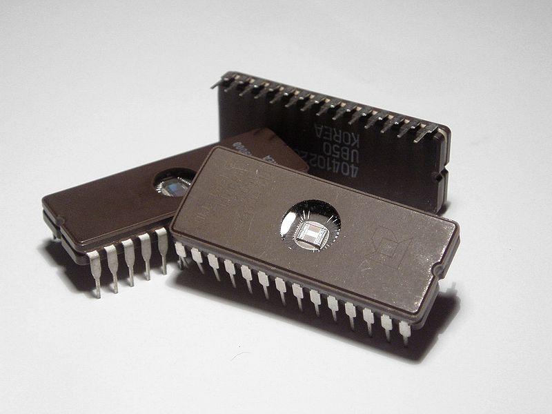
53 EPROM


54 Some Circuits
Analogue Electronics
 Università degli Studi di Roma Tor Vergata Dipartimento di Ingegneria Elettronica Analogue Electronics Paolo Colantonio A.A. 2015-16 Field-effect transistors Field-effect transistors (FETs) are probably
FUNDAMENTALS OF MODERN VLSI DEVICES
 19-13- FUNDAMENTALS OF MODERN VLSI DEVICES YUAN TAUR TAK H. MING CAMBRIDGE UNIVERSITY PRESS Physical Constants and Unit Conversions List of Symbols Preface page xi xiii xxi 1 INTRODUCTION I 1.1 Evolution
MOSFET short channel effects
 MOSFET short channel effects overview Five different short channel effects can be distinguished: velocity saturation drain induced barrier lowering (DIBL) impact ionization surface scattering hot electrons
EE301 Electronics I , Fall
 EE301 Electronics I 2018-2019, Fall 1. Introduction to Microelectronics (1 Week/3 Hrs.) Introduction, Historical Background, Basic Consepts 2. Rewiev of Semiconductors (1 Week/3 Hrs.) Semiconductor materials
INTERNATIONAL JOURNAL OF APPLIED ENGINEERING RESEARCH, DINDIGUL Volume 1, No 3, 2010
 Low Power CMOS Inverter design at different Technologies Vijay Kumar Sharma 1, Surender Soni 2 1 Department of Electronics & Communication, College of Engineering, Teerthanker Mahaveer University, Moradabad
Fin-Shaped Field Effect Transistor (FinFET) Min Ku Kim 03/07/2018
 Min Ku Kim 03/07/2018") Fin-Shaped Field Effect Transistor (FinFET) Min Ku Kim 03/07/2018 ECE 658 Sp 2018 Semiconductor Materials and Device Characterizations OUTLINE Background FinFET Future Roadmap Keeping up w/ Moore s Law
Fin-Shaped Field Effect Transistor (FinFET) Min Ku Kim 03/07/2018 ECE 658 Sp 2018 Semiconductor Materials and Device Characterizations OUTLINE Background FinFET Future Roadmap Keeping up w/ Moore s Law
Design cycle for MEMS
 Design cycle for MEMS Design cycle for ICs IC Process Selection nmos CMOS BiCMOS ECL for logic for I/O and driver circuit for critical high speed parts of the system The Real Estate of a Wafer MOS Transistor
INTRODUCTION TO MOS TECHNOLOGY
 INTRODUCTION TO MOS TECHNOLOGY 1. The MOS transistor The most basic element in the design of a large scale integrated circuit is the transistor. For the processes we will discuss, the type of transistor
Solid State Devices- Part- II. Module- IV
 Solid State Devices- Part- II Module- IV MOS Capacitor Two terminal MOS device MOS = Metal- Oxide- Semiconductor MOS capacitor - the heart of the MOSFET The MOS capacitor is used to induce charge at the
MICROPROCESSOR TECHNOLOGY
 MICROPROCESSOR TECHNOLOGY Assis. Prof. Hossam El-Din Moustafa Lecture 3 Ch.1 The Evolution of The Microprocessor 17-Feb-15 1 Chapter Objectives Introduce the microprocessor evolution from transistors to
EE70 - Intro. Electronics
 EE70 - Intro. Electronics Course website: ~/classes/ee70/fall05 Today s class agenda (November 28, 2005) review Serial/parallel resonant circuits Diode Field Effect Transistor (FET) f 0 = Qs = Qs = 1 2π
Semiconductor Physics and Devices
 Metal-Semiconductor and Semiconductor Heterojunctions The Metal-Oxide-Semiconductor Field-Effect Transistor (MOSFET) is one of two major types of transistors. The MOSFET is used in digital circuit, because
Intel s Breakthrough in High-K Gate Dielectric Drives Moore s Law Well into the Future
 Page 1 Intel s Breakthrough in High-K Gate Dielectric Drives Moore s Law Well into the Future Robert S. Chau Intel Fellow, Technology and Manufacturing Group Director, Transistor Research Intel Corporation
Lecture 4 - Digital Representations III + Transistors
 Lecture 4 - Digital Representations III + Transistors Video: Seems like a natural extension from images no? We just have a new dimension (time) Each frame is just an image made up of pixels Display n frames
UNIT-1 Fundamentals of Low Power VLSI Design
 UNIT-1 Fundamentals of Low Power VLSI Design Need for Low Power Circuit Design: The increasing prominence of portable systems and the need to limit power consumption (and hence, heat dissipation) in very-high
CHAPTER 2 LITERATURE REVIEW
 CHAPTER 2 LITERATURE REVIEW 2.1 Introduction of MOSFET The structure of the MOS field-effect transistor (MOSFET) has two regions of doping opposite that of the substrate, one at each edge of the MOS structure
Performance Evaluation of MISISFET- TCAD Simulation
 Performance Evaluation of MISISFET- TCAD Simulation Tarun Chaudhary Gargi Khanna Rajeevan Chandel ABSTRACT A novel device n-misisfet with a dielectric stack instead of the single insulator of n-mosfet
ECE520 VLSI Design. Lecture 2: Basic MOS Physics. Payman Zarkesh-Ha
 ECE520 VLSI Design Lecture 2: Basic MOS Physics Payman Zarkesh-Ha Office: ECE Bldg. 230B Office hours: Wednesday 2:00-3:00PM or by appointment E-mail: pzarkesh@unm.edu Slide: 1 Review of Last Lecture Semiconductor
Transistor was first invented by William.B.Shockley, Walter Brattain and John Bardeen of Bell Labratories. In 1961, first IC was introduced.
 Unit 1 Basic MOS Technology Transistor was first invented by William.B.Shockley, Walter Brattain and John Bardeen of Bell Labratories. In 1961, first IC was introduced. Levels of Integration:- i) SSI:-
Chapter 4. CMOS Cascode Amplifiers. 4.1 Introduction. 4.2 CMOS Cascode Amplifiers
 Chapter 4 CMOS Cascode Amplifiers 4.1 Introduction A single stage CMOS amplifier cannot give desired dc voltage gain, output resistance and transconductance. The voltage gain can be made to attain higher
Dual Metal Gate and Conventional MOSFET at Sub nm for Analog Application
 Dual Metal Gate and Conventional MOSFET at Sub nm for Analog Application Sonal Aggarwal 1 and Rajbir Singh 2 1 Department of Electronic Science, Kurukshetra university,kurukshetra sonal.aggarwal88@gmail.com
ECE 5745 Complex Digital ASIC Design Topic 2: CMOS Devices
 ECE 5745 Complex Digital ASIC Design Topic 2: CMOS Devices Christopher Batten School of Electrical and Computer Engineering Cornell University http://www.csl.cornell.edu/courses/ece5950 Simple Transistor
Lecture-45. MOS Field-Effect-Transistors Threshold voltage
 Lecture-45 MOS Field-Effect-Transistors 7.4. Threshold voltage In this section we summarize the calculation of the threshold voltage and discuss the dependence of the threshold voltage on the bias applied
Performance advancement of High-K dielectric MOSFET
 Performance advancement of High-K dielectric MOSFET Neha Thapa 1 Lalit Maurya 2 Er. Rajesh Mehra 3 M.E. Student M.E. Student Associate Prof. ECE NITTTR, Chandigarh NITTTR, Chandigarh NITTTR, Chandigarh
4: Transistors Non idealities
 4: Transistors Non idealities Inversion Major cause of non-idealities/complexities: Who controls channel (and how)? Large Body(Substrate) Source Voltage V G V SB - - - - - - - - n+ n+ - - - - - - - - -
Student Lecture by: Giangiacomo Groppi Joel Cassell Pierre Berthelot September 28 th 2004
 Student Lecture by: Giangiacomo Groppi Joel Cassell Pierre Berthelot September 28 th 2004 Lecture outline Historical introduction Semiconductor devices overview Bipolar Junction Transistor (BJT) Field
Physical Structure of CMOS Integrated Circuits
 Physical Structure of CMOS Integrated Circuits Dae Hyun Kim EECS Washington State University References John P. Uyemura, Introduction to VLSI Circuits and Systems, 2002. Chapter 3 Neil H. Weste and David
ECE 340 Lecture 37 : Metal- Insulator-Semiconductor FET Class Outline:
 ECE 340 Lecture 37 : Metal- Insulator-Semiconductor FET Class Outline: Metal-Semiconductor Junctions MOSFET Basic Operation MOS Capacitor Things you should know when you leave Key Questions What is the
Field-Effect Transistor (FET) is one of the two major transistors; FET derives its name from its working mechanism;
 is one of the two major transistors; FET derives its name from its working mechanism;") Chapter 3 Field-Effect Transistors (FETs) 3.1 Introduction Field-Effect Transistor (FET) is one of the two major transistors; FET derives its name from its working mechanism; The concept has been known
Chapter 3 Field-Effect Transistors (FETs) 3.1 Introduction Field-Effect Transistor (FET) is one of the two major transistors; FET derives its name from its working mechanism; The concept has been known
Session 10: Solid State Physics MOSFET
 Session 10: Solid State Physics MOSFET 1 Outline A B C D E F G H I J 2 MOSCap MOSFET Metal-Oxide-Semiconductor Field-Effect Transistor: Al (metal) SiO2 (oxide) High k ~0.1 ~5 A SiO2 A n+ n+ p-type Si (bulk)
NAME: Last First Signature
 UNIVERSITY OF CALIFORNIA, BERKELEY College of Engineering Department of Electrical Engineering and Computer Sciences EE 130: IC Devices Spring 2003 FINAL EXAMINATION NAME: Last First Signature STUDENT
UNIT-VI FIELD EFFECT TRANSISTOR. 1. Explain about the Field Effect Transistor and also mention types of FET s.
 UNIT-I FIELD EFFECT TRANSISTOR 1. Explain about the Field Effect Transistor and also mention types of FET s. The Field Effect Transistor, or simply FET however, uses the voltage that is applied to their
INTRODUCTION: Basic operating principle of a MOSFET:
 INTRODUCTION: Along with the Junction Field Effect Transistor (JFET), there is another type of Field Effect Transistor available whose Gate input is electrically insulated from the main current carrying
Chapter 3: Basics Semiconductor Devices and Processing 2006/9/27 1. Topics
 Chapter 3: Basics Semiconductor Devices and Processing 2006/9/27 1 Topics What is semiconductor Basic semiconductor devices Basics of IC processing CMOS technologies 2006/9/27 2 1 What is Semiconductor
Electrical Characterization of a Second-gate in a Silicon-on-Insulator Transistor
 Electrical Characterization of a Second-gate in a Silicon-on-Insulator Transistor Antonio Oblea: McNair Scholar Dr. Stephen Parke: Faculty Mentor Electrical Engineering As an independent double-gate, silicon-on-insulator
Basic Fabrication Steps
 Basic Fabrication Steps and Layout Somayyeh Koohi Department of Computer Engineering Adapted with modifications from lecture notes prepared by author Outline Fabrication steps Transistor structures Transistor
4 principal of JNTU college of Eng., JNTUH, Kukatpally, Hyderabad, A.P, INDIA
 Efficient Power Management Technique for Deep-Submicron Circuits P.Sreenivasulu 1, Ch.Aruna 2 Dr. K.Srinivasa Rao 3, Dr. A.Vinaya babu 4 1 Research Scholar, ECE Department, JNTU Kakinada, A.P, INDIA. 2
Chapter 3 Basics Semiconductor Devices and Processing
 Chapter 3 Basics Semiconductor Devices and Processing 1 Objectives Identify at least two semiconductor materials from the periodic table of elements List n-type and p-type dopants Describe a diode and
DG-FINFET LOGIC DESIGN USING 32NM TECHNOLOGY
 International Journal of Knowledge Management & e-learning Volume 3 Number 1 January-June 2011 pp. 1-5 DG-FINFET LOGIC DESIGN USING 32NM TECHNOLOGY K. Nagarjuna Reddy 1, K. V. Ramanaiah 2 & K. Sudheer
3084 IEEE TRANSACTIONS ON NUCLEAR SCIENCE, VOL. 60, NO. 4, AUGUST 2013
 3084 IEEE TRANSACTIONS ON NUCLEAR SCIENCE, VOL. 60, NO. 4, AUGUST 2013 Dummy Gate-Assisted n-mosfet Layout for a Radiation-Tolerant Integrated Circuit Min Su Lee and Hee Chul Lee Abstract A dummy gate-assisted
Contents 1 Introduction 2 MOS Fabrication Technology
 Contents 1 Introduction... 1 1.1 Introduction... 1 1.2 Historical Background [1]... 2 1.3 Why Low Power? [2]... 7 1.4 Sources of Power Dissipations [3]... 9 1.4.1 Dynamic Power... 10 1.4.2 Static Power...
MOSFET & IC Basics - GATE Problems (Part - I)
") MOSFET & IC Basics - GATE Problems (Part - I) 1. Channel current is reduced on application of a more positive voltage to the GATE of the depletion mode n channel MOSFET. (True/False) [GATE 1994: 1 Mark]
MOSFET & IC Basics - GATE Problems (Part - I) 1. Channel current is reduced on application of a more positive voltage to the GATE of the depletion mode n channel MOSFET. (True/False) [GATE 1994: 1 Mark]
Lecture 4. MOS transistor theory
 Lecture 4 MOS transistor theory 1.7 Introduction: A MOS transistor is a majority-carrier device, in which the current in a conducting channel between the source and the drain is modulated by a voltage
Depletion-mode operation ( 공핍형 ): Using an input gate voltage to effectively decrease the channel size of an FET
: Using an input gate voltage to effectively decrease the channel size of an FET") Ch. 13 MOSFET Metal-Oxide-Semiconductor Field-Effect Transistor : I D D-mode E-mode V g The gate oxide is made of dielectric SiO 2 with e = 3.9 Depletion-mode operation ( 공핍형 ): Using an input gate voltage
Ch. 13 MOSFET Metal-Oxide-Semiconductor Field-Effect Transistor : I D D-mode E-mode V g The gate oxide is made of dielectric SiO 2 with e = 3.9 Depletion-mode operation ( 공핍형 ): Using an input gate voltage
444 Index. F Fermi potential, 146 FGMOS transistor, 20 23, 57, 83, 84, 98, 205, 208, 213, 215, 216, 241, 242, 251, 280, 311, 318, 332, 354, 407
 Index A Accuracy active resistor structures, 46, 323, 328, 329, 341, 344, 360 computational circuits, 171 differential amplifiers, 30, 31 exponential circuits, 285, 291, 292 multifunctional structures,
Conduction Characteristics of MOS Transistors (for fixed Vds)! Topic 2. Basic MOS theory & SPICE simulation. MOS Transistor
! Topic 2. Basic MOS theory & SPICE simulation. MOS Transistor") Conduction Characteristics of MOS Transistors (for fixed Vds)! Topic 2 Basic MOS theory & SPICE simulation Peter Cheung Department of Electrical & Electronic Engineering Imperial College London (Weste&Harris,
Conduction Characteristics of MOS Transistors (for fixed Vds)! Topic 2 Basic MOS theory & SPICE simulation Peter Cheung Department of Electrical & Electronic Engineering Imperial College London (Weste&Harris,
Topic 2. Basic MOS theory & SPICE simulation
 Topic 2 Basic MOS theory & SPICE simulation Peter Cheung Department of Electrical & Electronic Engineering Imperial College London (Weste&Harris, Ch 2 & 5.1-5.3 Rabaey, Ch 3) URL: www.ee.ic.ac.uk/pcheung/
Conduction Characteristics of MOS Transistors (for fixed Vds) Topic 2. Basic MOS theory & SPICE simulation. MOS Transistor
 Topic 2. Basic MOS theory & SPICE simulation. MOS Transistor") Conduction Characteristics of MOS Transistors (for fixed Vds) Topic 2 Basic MOS theory & SPICE simulation Peter Cheung Department of Electrical & Electronic Engineering Imperial College London (Weste&Harris,
Conduction Characteristics of MOS Transistors (for fixed Vds) Topic 2 Basic MOS theory & SPICE simulation Peter Cheung Department of Electrical & Electronic Engineering Imperial College London (Weste&Harris,
EE 42/100 Lecture 23: CMOS Transistors and Logic Gates. Rev A 4/15/2012 (10:39 AM) Prof. Ali M. Niknejad
 Prof. Ali M. Niknejad") A. M. Niknejad University of California, Berkeley EE 100 / 42 Lecture 23 p. 1/16 EE 42/100 Lecture 23: CMOS Transistors and Logic Gates ELECTRONICS Rev A 4/15/2012 (10:39 AM) Prof. Ali M. Niknejad University
A. M. Niknejad University of California, Berkeley EE 100 / 42 Lecture 23 p. 1/16 EE 42/100 Lecture 23: CMOS Transistors and Logic Gates ELECTRONICS Rev A 4/15/2012 (10:39 AM) Prof. Ali M. Niknejad University
Lecture #29. Moore s Law
 Lecture #29 ANNOUNCEMENTS HW#15 will be for extra credit Quiz #6 (Thursday 5/8) will include MOSFET C-V No late Projects will be accepted after Thursday 5/8 The last Coffee Hour will be held this Thursday
Field-Effect Transistors
 R L 2 Field-Effect Transistors 2.1 BAIC PRINCIPLE OF JFET The eld-effect transistor (FET) is an electric- eld (voltage) operated transistor, developed as a semiconductor equivalent of the vacuum-tube device,
3: MOS Transistors. Non idealities
 3: MOS Transistors Non idealities Inversion Major cause of non-idealities/complexities: Who controls channel (and how)? Large Body(Substrate) Source Voltage V G V SB - - - - - - - - n+ n+ - - - - - - -
SEMICONDUCTOR ELECTRONICS: MATERIALS, DEVICES AND SIMPLE CIRCUITS. Class XII : PHYSICS WORKSHEET
 SEMICONDUCT ELECTRONICS: MATERIALS, DEVICES AND SIMPLE CIRCUITS Class XII : PHYSICS WKSHEET 1. How is a n-p-n transistor represented symbolically? (1) 2. How does conductivity of a semiconductor change
Optimization of Direct Tunneling Gate Leakage Current in Ultrathin Gate Oxide FET with High-K Dielectrics
 Optimization of Direct Tunneling Gate Leakage Current in Ultrathin Gate Oxide FET with High-K Dielectrics Sweta Chander 1, Pragati Singh 2, S Baishya 3 1,2,3 Department of Electronics & Communication Engineering,
White Paper Stratix III Programmable Power
 Introduction White Paper Stratix III Programmable Power Traditionally, digital logic has not consumed significant static power, but this has changed with very small process nodes. Leakage current in digital
CONTENTS. 2.2 Schrodinger's Wave Equation 31. PART I Semiconductor Material Properties. 2.3 Applications of Schrodinger's Wave Equation 34
 CONTENTS Preface x Prologue Semiconductors and the Integrated Circuit xvii PART I Semiconductor Material Properties CHAPTER 1 The Crystal Structure of Solids 1 1.0 Preview 1 1.1 Semiconductor Materials
LEAKAGE POWER REDUCTION TECHNIQUES FOR LOW POWER VLSI DESIGN: A REVIEW PAPER
 International Journal Of Advance Research In Science And Engineering http:// LEAKAGE POWER REDUCTION TECHNIQUES FOR LOW POWER VLSI DESIGN: A REVIEW PAPER Raju Hebbale 1, Pallavi Hiremath 2 1,2 Department
Notes. (Subject Code: 7EC5)
") COMPUCOM INSTITUTE OF TECHNOLOGY & MANAGEMENT, JAIPUR (DEPARTMENT OF ELECTRONICS & COMMUNICATION) Notes VLSI DESIGN NOTES (Subject Code: 7EC5) Prepared By: MANVENDRA SINGH Class: B. Tech. IV Year, VII
COMPUCOM INSTITUTE OF TECHNOLOGY & MANAGEMENT, JAIPUR (DEPARTMENT OF ELECTRONICS & COMMUNICATION) Notes VLSI DESIGN NOTES (Subject Code: 7EC5) Prepared By: MANVENDRA SINGH Class: B. Tech. IV Year, VII
PROCESS-VOLTAGE-TEMPERATURE (PVT) VARIATIONS AND STATIC TIMING ANALYSIS
 VARIATIONS AND STATIC TIMING ANALYSIS") PROCESS-VOLTAGE-TEMPERATURE (PVT) VARIATIONS AND STATIC TIMING ANALYSIS The major design challenges of ASIC design consist of microscopic issues and macroscopic issues [1]. The microscopic issues are ultra-high
PROCESS-VOLTAGE-TEMPERATURE (PVT) VARIATIONS AND STATIC TIMING ANALYSIS The major design challenges of ASIC design consist of microscopic issues and macroscopic issues [1]. The microscopic issues are ultra-high
UNIT III VLSI CIRCUIT DESIGN PROCESSES. In this chapter we will be studying how to get the schematic into stick diagrams or layouts.
 UNIT III VLSI CIRCUIT DESIGN PROCESSES In this chapter we will be studying how to get the schematic into stick diagrams or layouts. MOS circuits are formed on four basic layers: N-diffusion P-diffusion
Semiconductor Process Reliability SVTW 2012 Esko Mikkola, Ph.D. & Andrew Levy
 Semiconductor Process Reliability SVTW 2012 Esko Mikkola, Ph.D. & Andrew Levy 1 IC Failure Modes Affecting Reliability Via/metallization failure mechanisms Electro migration Stress migration Transistor
Dual-K K Versus Dual-T T Technique for Gate Leakage Reduction : A Comparative Perspective
 Dual-K K Versus Dual-T T Technique for Gate Leakage Reduction : A Comparative Perspective S. P. Mohanty, R. Velagapudi and E. Kougianos Dept of Computer Science and Engineering University of North Texas
EMT 251 Introduction to IC Design
 EMT 251 Introduction to IC Design (Pengantar Rekabentuk Litar Terkamir) Semester II 2011/2012 Introduction to IC design and Transistor Fundamental Some Keywords! Very-large-scale-integration (VLSI) is
Design and Analysis of Double Gate MOSFET Devices using High-k Dielectric
 International Journal of Electrical Engineering. ISSN 0974-2158 Volume 7, Number 1 (2014), pp. 53-60 International Research Publication House http://www.irphouse.com Design and Analysis of Double Gate
Future MOSFET Devices using high-k (TiO 2 ) dielectric
 dielectric") Future MOSFET Devices using high-k (TiO 2 ) dielectric Prerna Guru Jambheshwar University, G.J.U.S. & T., Hisar, Haryana, India, prernaa.29@gmail.com Abstract: In this paper, an 80nm NMOS with high-k (TiO
Future MOSFET Devices using high-k (TiO 2 ) dielectric Prerna Guru Jambheshwar University, G.J.U.S. & T., Hisar, Haryana, India, prernaa.29@gmail.com Abstract: In this paper, an 80nm NMOS with high-k (TiO
EECS130 Integrated Circuit Devices
 EECS130 Integrated Circuit Devices Professor Ali Javey 11/01/2007 MOSFETs Lecture 5 Announcements HW7 set is due now HW8 is assigned, but will not be collected/graded. MOSFET Technology Scaling Technology
ATV 2011: Computer Engineering
 ATV 2011: Technology Trends in Computer Engineering Professor Per Larsson-Edefors ATV 2011, L1, Per Larsson-Edefors Page 1 Solid-State Devices www.cse.chalmers.se/~perla/ugrad/ SemTech/Lectures_2000.pdf
55:041 Electronic Circuits
 55:041 Electronic Circuits Mosfet Review Sections of Chapter 3 &4 A. Kruger Mosfet Review, Page-1 Basic Structure of MOS Capacitor Sect. 3.1 Width 1 10-6 m or less Thickness 50 10-9 m or less ` MOS Metal-Oxide-Semiconductor
Three Terminal Devices
 Three Terminal Devices - field effect transistor (FET) - bipolar junction transistor (BJT) - foundation on which modern electronics is built - active devices - devices described completely by considering
value of W max for the device. The at band voltage is -0.9 V. Problem 5: An Al-gate n-channel MOS capacitor has a doping of N a = cm ;3. The oxi
 Prof. Jasprit Singh Fall 2001 EECS 320 Homework 10 This homework is due on December 6 Problem 1: An n-type In 0:53 Ga 0:47 As epitaxial layer doped at 10 16 cm ;3 is to be used as a channel in a FET. A
Alternatives to standard MOSFETs. What problems are we really trying to solve?
 Alternatives to standard MOSFETs A number of alternative FET schemes have been proposed, with an eye toward scaling up to the 10 nm node. Modifications to the standard MOSFET include: Silicon-in-insulator
FET(Field Effect Transistor)
") Field Effect Transistor: Construction and Characteristic of JFETs. Transfer Characteristic. CS,CD,CG amplifier and analysis of CS amplifier MOSFET (Depletion and Enhancement) Type, Transfer Characteristic,
Field Effect Transistor: Construction and Characteristic of JFETs. Transfer Characteristic. CS,CD,CG amplifier and analysis of CS amplifier MOSFET (Depletion and Enhancement) Type, Transfer Characteristic,
Prof. Paolo Colantonio a.a
 Prof. Paolo Colantonio a.a. 20 2 Field effect transistors (FETs) are probably the simplest form of transistor, widely used in both analogue and digital applications They are characterised by a very high
Lesson 5. Electronics: Semiconductors Doping p-n Junction Diode Half Wave and Full Wave Rectification Introduction to Transistors-
 Lesson 5 Electronics: Semiconductors Doping p-n Junction Diode Half Wave and Full Wave Rectification Introduction to Transistors- Types and Connections Semiconductors Semiconductors If there are many free
EE4800 CMOS Digital IC Design & Analysis. Lecture 1 Introduction Zhuo Feng
 EE4800 CMOS Digital IC Design & Analysis Lecture 1 Introduction Zhuo Feng 1.1 Prof. Zhuo Feng Office: EERC 730 Phone: 487-3116 Email: zhuofeng@mtu.edu Class Website http://www.ece.mtu.edu/~zhuofeng/ee4800fall2010.html
Energy Consumption Issues and Power Management Techniques
 Energy Consumption Issues and Power Management Techniques David Macii Embedded Electronics and Computing Systems group http://eecs.disi.unitn.it The scenario 2 The Moore s Law The transistor count in IC
Module-3: Metal Oxide Semiconductor (MOS) & Emitter coupled logic (ECL) families
 & Emitter coupled logic (ECL) families") 1 Module-3: Metal Oxide Semiconductor (MOS) & Emitter coupled logic (ECL) families 1. Introduction 2. Metal Oxide Semiconductor (MOS) logic 2.1. Enhancement and depletion mode 2.2. NMOS and PMOS inverter
1 Module-3: Metal Oxide Semiconductor (MOS) & Emitter coupled logic (ECL) families 1. Introduction 2. Metal Oxide Semiconductor (MOS) logic 2.1. Enhancement and depletion mode 2.2. NMOS and PMOS inverter
4.1 Device Structure and Physical Operation
 10/12/2004 4_1 Device Structure and Physical Operation blank.doc 1/2 4.1 Device Structure and Physical Operation Reading Assignment: pp. 235-248 Chapter 4 covers Field Effect Transistors ( ) Specifically,
55:041 Electronic Circuits
 55:041 Electronic Circuits MOSFETs Sections of Chapter 3 &4 A. Kruger MOSFETs, Page-1 Basic Structure of MOS Capacitor Sect. 3.1 Width = 1 10-6 m or less Thickness = 50 10-9 m or less ` MOS Metal-Oxide-Semiconductor
SCALING AND NUMERICAL SIMULATION ANALYSIS OF 50nm MOSFET INCORPORATING DIELECTRIC POCKET (DP-MOSFET)
") SCALING AND NUMERICAL SIMULATION ANALYSIS OF 50nm MOSFET INCORPORATING DIELECTRIC POCKET (DP-MOSFET) Zul Atfyi Fauzan M. N., Ismail Saad and Razali Ismail Faculty of Electrical Engineering, Universiti
SCALING AND NUMERICAL SIMULATION ANALYSIS OF 50nm MOSFET INCORPORATING DIELECTRIC POCKET (DP-MOSFET) Zul Atfyi Fauzan M. N., Ismail Saad and Razali Ismail Faculty of Electrical Engineering, Universiti
EE105 Fall 2015 Microelectronic Devices and Circuits: MOSFET Prof. Ming C. Wu 511 Sutardja Dai Hall (SDH)
") EE105 Fall 2015 Microelectronic Devices and Circuits: MOSFET Prof. Ming C. Wu wu@eecs.berkeley.edu 511 Sutardja Dai Hall (SDH) 7-1 Simplest Model of MOSFET (from EE16B) 7-2 CMOS Inverter 7-3 CMOS NAND
EE105 Fall 2015 Microelectronic Devices and Circuits: MOSFET Prof. Ming C. Wu wu@eecs.berkeley.edu 511 Sutardja Dai Hall (SDH) 7-1 Simplest Model of MOSFET (from EE16B) 7-2 CMOS Inverter 7-3 CMOS NAND
SRM INSTITUTE OF SCIENCE AND TECHNOLOGY (DEEMED UNIVERSITY)
") SRM INSTITUTE OF SCIENCE AND TECHNOLOGY (DEEMED UNIVERSITY) QUESTION BANK I YEAR B.Tech (II Semester) ELECTRONIC DEVICES (COMMON FOR EC102, EE104, IC108, BM106) UNIT-I PART-A 1. What are intrinsic and
SRM INSTITUTE OF SCIENCE AND TECHNOLOGY (DEEMED UNIVERSITY) QUESTION BANK I YEAR B.Tech (II Semester) ELECTRONIC DEVICES (COMMON FOR EC102, EE104, IC108, BM106) UNIT-I PART-A 1. What are intrinsic and
UNIVERSITY OF CALIFORNIA AT BERKELEY College of Engineering Department of Electrical Engineering and Computer Sciences.
 UNIVERSITY OF CALIFORNIA AT BERKELEY College of Engineering Department of Electrical Engineering and Computer Sciences Discussion #9 EE 05 Spring 2008 Prof. u MOSFETs The standard MOSFET structure is shown
Static Power and the Importance of Realistic Junction Temperature Analysis
 White Paper: Virtex-4 Family R WP221 (v1.0) March 23, 2005 Static Power and the Importance of Realistic Junction Temperature Analysis By: Matt Klein Total power consumption of a board or system is important;
Performance Comparison of CMOS and Finfet Based Circuits At 45nm Technology Using SPICE
 RESEARCH ARTICLE OPEN ACCESS Performance Comparison of CMOS and Finfet Based Circuits At 45nm Technology Using SPICE Mugdha Sathe*, Dr. Nisha Sarwade** *(Department of Electrical Engineering, VJTI, Mumbai-19)
Gallium nitride (GaN)
") 80 Technology focus: GaN power electronics Vertical, CMOS and dual-gate approaches to gallium nitride power electronics US research company HRL Laboratories has published a number of papers concerning
80 Technology focus: GaN power electronics Vertical, CMOS and dual-gate approaches to gallium nitride power electronics US research company HRL Laboratories has published a number of papers concerning
420 Intro to VLSI Design
 Dept of Electrical and Computer Engineering 420 Intro to VLSI Design Lecture 0: Course Introduction and Overview Valencia M. Joyner Spring 2005 Getting Started Syllabus About the Instructor Labs, Problem
Design Simulation and Analysis of NMOS Characteristics for Varying Oxide Thickness
 MIT International Journal of Electronics and Communication Engineering, Vol. 4, No. 2, August 2014, pp. 81 85 81 Design Simulation and Analysis of NMOS Characteristics for Varying Oxide Thickness Alpana
Pramoda N V Department of Electronics and Communication Engineering, MCE Hassan Karnataka India
 Advanced Low Power CMOS Design to Reduce Power Consumption in CMOS Circuit for VLSI Design Pramoda N V Department of Electronics and Communication Engineering, MCE Hassan Karnataka India Abstract: Low
PAPER SOLUTION_DECEMBER_2014_VLSI_DESIGN_ETRX_SEM_VII Prepared by Girish Gidaye
 Q1a) The MOS System under External Bias Depending on the polarity and the magnitude of V G, three different operating regions can be observed for the MOS system: 1) Accumulation 2) Depletion 3) Inversion
CMOS Technology. 1. Why CMOS 2. Qualitative MOSFET model 3. Building a MOSFET 4. CMOS logic gates. Handouts: Lecture Slides. metal ndiff.
 CMOS Technology 1. Why CMOS 2. Qualitative MOSFET model 3. Building a MOSFET 4. CMOS logic gates poly pdiff metal ndiff Handouts: Lecture Slides L03 - CMOS Technology 1 Building Bits from Atoms V in V
(Refer Slide Time: 02:05)
") Electronics for Analog Signal Processing - I Prof. K. Radhakrishna Rao Department of Electrical Engineering Indian Institute of Technology Madras Lecture 27 Construction of a MOSFET (Refer Slide Time:
Electronics for Analog Signal Processing - I Prof. K. Radhakrishna Rao Department of Electrical Engineering Indian Institute of Technology Madras Lecture 27 Construction of a MOSFET (Refer Slide Time:
LEAKAGE POWER REDUCTION IN CMOS CIRCUITS USING LEAKAGE CONTROL TRANSISTOR TECHNIQUE IN NANOSCALE TECHNOLOGY
 LEAKAGE POWER REDUCTION IN CMOS CIRCUITS USING LEAKAGE CONTROL TRANSISTOR TECHNIQUE IN NANOSCALE TECHNOLOGY Abhishek Sharma 1,Shipra Mishra 2 1 M.Tech. Embedded system & VLSI Design NITM,Gwalior M.P. India
Variation-Aware Design for Nanometer Generation LSI
 HIRATA Morihisa, SHIMIZU Takashi, YAMADA Kenta Abstract Advancement in the microfabrication of semiconductor chips has made the variations and layout-dependent fluctuations of transistor characteristics
MOS TRANSISTOR THEORY
 MOS TRANSISTOR THEORY Introduction A MOS transistor is a majority-carrier device, in which the current in a conducting channel between the source and the drain is modulated by a voltage applied to the
CHAPTER FORMULAS & NOTES
 Formulae For u SEMICONDUCTORS By Mir Mohammed Abbas II PCMB 'A' 1 Important Terms, Definitions & Formulae CHAPTER FORMULAS & NOTES 1 Intrinsic Semiconductor: The pure semiconductors in which the electrical
TECHNO INDIA BATANAGAR (DEPARTMENT OF ELECTRONICS & COMMUNICATION ENGINEERING) QUESTION BANK- 2018
 QUESTION BANK- 2018") TECHNO INDIA BATANAGAR (DEPARTMENT OF ELECTRONICS & COMMUNICATION ENGINEERING) QUESTION BANK- 2018 Paper Setter Detail Name Designation Mobile No. E-mail ID Raina Modak Assistant Professor 6290025725 raina.modak@tib.edu.in
TECHNO INDIA BATANAGAR (DEPARTMENT OF ELECTRONICS & COMMUNICATION ENGINEERING) QUESTION BANK- 2018 Paper Setter Detail Name Designation Mobile No. E-mail ID Raina Modak Assistant Professor 6290025725 raina.modak@tib.edu.in
UNIT 3: FIELD EFFECT TRANSISTORS
 FIELD EFFECT TRANSISTOR: UNIT 3: FIELD EFFECT TRANSISTORS The field effect transistor is a semiconductor device, which depends for its operation on the control of current by an electric field. There are
Field Effect Transistors (npn)
") Field Effect Transistors (npn) gate drain source FET 3 terminal device channel e - current from source to drain controlled by the electric field generated by the gate base collector emitter BJT 3 terminal
Field Effect Transistors (npn) gate drain source FET 3 terminal device channel e - current from source to drain controlled by the electric field generated by the gate base collector emitter BJT 3 terminal
2014, IJARCSSE All Rights Reserved Page 1352
 Volume 4, Issue 3, March 2014 ISSN: 2277 128X International Journal of Advanced Research in Computer Science and Software Engineering Research Paper Available online at: www.ijarcsse.com Double Gate N-MOSFET