Nanoscale switching in resistive memory structures
|
|
|
- Hortense Golden
- 5 years ago
- Views:
Transcription


1 Nanoscale switching in resistive memory structures D. Deleruyelle, C. Dumas, M. Carmona, Ch. Muller IM2NP UMR CNRS 6242 & Institut Carnot STAR Polytech Marseille, Université de Provence IMT Technopôle de Château Gombert Marseille Cedex 20 e mail: christophe.muller@im2np.fr Innovative Memory Technologies Minatec Grenoble France
2 Partners in EMMA* project MDM (Milano Italy) S. Spiga, A. Lamperti, and M. Fanciulli Numonyx (Milano Italy) I. Tortorelli, R. Bez IMEC (Leuven Belgium) R. Müller, L. Goux, D.J. Wouters * Emerging Materials for Mass storage Architectures FP6 IST no
3 Outline 1. Context 2. Nanoscale switching in CuTCNQ-based memory structures 3. Nanoscale switching in NiO film on top of pillar bottom electrode 4. Summary
4 Outline 1. Context 2. Nanoscale switching in CuTCNQ-based memory structures 3. Nanoscale switching in NiO film on top of pillar bottom electrode 4. Summary


5 Key players on resistive systems


6 Latest ITRS classification (partial) Types Nanothermal High resistance "0" Logical states Low resistance "1" Materials Transition metal oxide (TMO) Chalcogenide nanowires for PCM Nanomechanical Suspended CNT Nanowires Nanorods Nanoionic Organic complex Oxide Chalcogenide


7 Nanothermal devices (TMO) Fujitsu (TiO 2 ) Samsung (NiO) Matsushita (FeO x ) Hynix (TiO 2 ) Spansion (Cu 2 O) Fujitsu (Ti doped NiO)


 NIMS Memristor")

 HP Unity")
8 Qimonda Nanoionic devices Ionic transport combined with redox process in a solid electrolyte o Anions (e.g. O 2 ) NIMS Memristor (HP), CMOx (Unity), o Cations (e.g. Ag + ) CBRAM (Qimonda, NIMS, Adesto, ) HP Unity Adesto 4F 2 /8 bits = 0.5F 2
9 Outline 1. Context 2. Nanoscale switching in CuTCNQ-based memory structures 3. Nanoscale switching in NiO film on top of pillar bottom electrode 4. Summary


10 Metal organic complex CuTCNQ Copper-tetracyanoquinodimethane CuTCNQ may grow in small dimension via holes o High density & low cost memory devices Gas/solid reaction or growth in solution Bipolar resistive switching Demolliens et al., J. Cryst. Growth, submitted

11 CuTCNQ nanowires on HfO 2 layer CuTCNQ nanowires Au (TE) HfO 2 (switching layer) Pt (BE) CuTCNQ nanowires grown on 3 nm thick HfO 2 "switching layer" (SL) o Copper transport within HfO 2 switching layer Creation/dissolution of conductive bridges o Improved electrical performances Muller et al., Solid-State Electronics, Submitted

 o Clockwise on")


12 Switching characteristics Bipolar resistance switching (RS) o Clockwise on pad-size devices o Anticlockwise at nanoscale At nanoscale, RS governed by a nano-gap between AFM tip and CuTCNQ nanowires
 Basic local memory operations achieved under bias voltage o Set/Reset/Read Muller et al.")
13 An additional proof Au Cu (BE) Complementary C-AFM experiments performed on CuTCNQ(nanowires)/Cu(BE) (without oxide switching layer) Basic local memory operations achieved under bias voltage o Set/Reset/Read Muller et al., Solid-State Electronics, Submitted


14 Redox process Cu + Nano-gap Cu Cu + Cu + Cu Cu Cu CuTCNQ Nano-gap Cu + Cu + Cu Cu Cu Cu CuTCNQ


![mechanism J(x,t) = qµ Cu+ [Cu + ] D Cu+](/docs-images/92/108448400/images/15-4.jpg "[Cu + ] x + S SL Einstein relationship")
15 Modeling V Top V Top Nano-gap = SL Cu + t CF tsl R SL Cu Cu Cu Cu CuTCNQ R CuTCNQ V Bottom Equivalent resistance of the stack t SL t CF R TOT = R SL + R CuTCNQ with R SL = SL Transport of Cu + ions governed by drift-diffusion mechanism J(x,t) = qµ Cu+ [Cu + ] D Cu+ [Cu + ] x + S SL Einstein relationship and continuity equation
16 Actual nanoionic device Satisfactory agreement between AFM measurements and model This model can be transposed to copper transport within HfO 2 switching layer Oxidation process at CuTCNQ surface o Cu Cu + + 1e Transport of Cu + ions from CuTCNQ to AFM tip Reduction process at AFM tip o Cu + + 1e Cu Growth of conductive filaments from AFM tip to CuTCNQ surface Redox set operation HRS LRS Deleruyelle et al., Appl. Phys. Lett., vol. 96, no. 26, pp (1-3), 2010
17 Outline 1. Context 2. Nanoscale switching in CuTCNQ-based memory structures 3. Nanoscale switching in NiO film on top of pillar bottom electrode 4. Summary

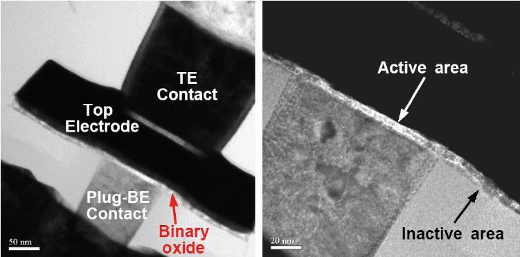
18 Memory devices Electrical characterization on conventional probe station Conductive AFM (C-AFM) measurements TE Pt NiO ALD Pt BE AFM tip NiO Silver paste SiO 2 SiO 2 Si 3 N 4 CoSi 2 Si 3 N 4 CoSi 2 Si Si W-plug Spiga et al., Proc. of MRS Spring Meeting, 2009 Demolliens et al., IEEE Proc. of Int. Memory Workshop, 2009

 SiO 2 Si 3 N 4 50 nm")

19 Microstructure TEM cross-section AFM topography Pt NiO 200 nm Imprint of underlying W-plug W (180 nm) SiO 2 Si 3 N 4 50 nm CoSi 2 Bending of NiO film due to a dishing of W-plugs during CMP process


20 Experimental protocol Program Set & Reset Read B-doped diamond Pt-Ir


21 Forming/set operation Superimposition of topography and current mapping Initial state V Prog = 1 V V Prog = 2 V V Prog = 3 V 1.5 µm V Read = 1 mv No conductive spots in initial state o High resistance state Gradual appearance and growth of highly conductive regions (around 20 to 30 nm) when increasing programming bias o Emulation of forming/set operation
22 Reset operation Superimposition of topography and current mapping Initial state V Prog = 5 V V Prog = 4.5 V 1.5 µm V Read = 1 mv Dissolution of conductive filaments at high voltage o Reset operation achieved! Some residual conductive regions still remain after local reset


23 Superimposition of topography and current mapping Retention 2 days 13 days 21 days 30 days 1.5 µm V Read = 1 mv Initial forming and read of programmed area Some conductive filaments remain after 30 days o Retention demonstrated at nanoscale Decrease of filament diameter in time
24 Actual nanothermal device Initial insulating state LRS: multiple conductive regions within NiO film HRS: only few residual conductive filaments after reset
25 Outline 1. Context 2. Nanoscale switching in CuTCNQ-based memory structures 3. Nanoscale switching in NiO film on top of pillar bottom electrode 4. Summary


 Joule effect enabling")


26 Summary Memory cell structure Polarity of switching Switching classification Basic mechanism Size limits Reset operation NiO deposited on top of pillar W electrode Unipolar Nanothermal Filamentary Filament diameter (20 nm) Joule effect enabling filament dissolution CuTCNQbased memory elements Bipolar Nanoionic Filamentary Area around tip Redox process Switching demonstrated at nanoscale in both systems! o Scalabilty conditioned by a tight control of filaments
27 Thank you for your attention
Fabrication and Characterization of Emerging Nanoscale Memory
 Fabrication and Characterization of Emerging Nanoscale Memory Yuan Zhang, SangBum Kim, Byoungil Lee, Marissa Caldwell(*), and (*) Chemistry Department Stanford University, Stanford, California, U.S.A.
Non-Volatile Memory Based on Solid Electrolytes
 Non-Volatile Memory Based on Solid Electrolytes Michael Kozicki Chakku Gopalan Murali Balakrishnan Mira Park Maria Mitkova Center for Solid State Electronics Research Introduction The electrochemical redistribution
HfO 2 Based Resistive Switching Non-Volatile Memory (RRAM) and Its Potential for Embedded Applications
 and Its Potential for Embedded Applications") 2012 International Conference on Solid-State and Integrated Circuit (ICSIC 2012) IPCSIT vol. 32 (2012) (2012) IACSIT Press, Singapore HfO 2 Based Resistive Switching Non-Volatile Memory (RRAM) and Its
2012 International Conference on Solid-State and Integrated Circuit (ICSIC 2012) IPCSIT vol. 32 (2012) (2012) IACSIT Press, Singapore HfO 2 Based Resistive Switching Non-Volatile Memory (RRAM) and Its
Conductance switching in Ag 2 S devices fabricated by sulphurization
 3 Conductance switching in Ag S devices fabricated by sulphurization The electrical characterization and switching properties of the α-ag S thin films fabricated by sulfurization are presented in this
In pursuit of high-density storage class memory
 Edition October 2017 Semiconductor technology & processing In pursuit of high-density storage class memory A novel thermally stable GeSe-based selector paves the way to storage class memory applications.
Resistive Switching Memory in Integration
 EDS Mini Colloquim WIMNACT 39, Tokyo Resistive Switching Memory in Integration Ming Liu Institute of Microelectronics, CAS Feb.7, 2014 Outline Motivation RRAM Integration Self-Rectifying RRAM 1D1R Integration
Supplementary Materials for
 advances.sciencemag.org/cgi/content/full/2/6/e1501326/dc1 Supplementary Materials for Organic core-sheath nanowire artificial synapses with femtojoule energy consumption Wentao Xu, Sung-Yong Min, Hyunsang
Analog Synaptic Behavior of a Silicon Nitride Memristor
 Supporting Information Analog Synaptic Behavior of a Silicon Nitride Memristor Sungjun Kim, *, Hyungjin Kim, Sungmin Hwang, Min-Hwi Kim, Yao-Feng Chang,, and Byung-Gook Park *, Inter-university Semiconductor
Supplementary Information
 Normalized Intensity Current (A) Supplementary Information 10-2 10-3 10-4 10-5 10-6 10-7 10-8 10-9 30x30 m 2 V set V reset Electroforming Pt/ / /Pt 10-10 -4-3 -2-1 0 1 2 3 4 5 Voltage (V) Pt/ / /SiO 2
INVESTIGATION OF RESISTIVE SWITCHING AND CONDUCTION MECHANISMS IN OXIDE-BASED RRAM DEVICE FOR EMERGING NONVOLATILE MEMORY APPLICATIONS
 INVESTIGATION OF RESISTIVE SWITCHING AND CONDUCTION MECHANISMS IN OXIDE-BASED RRAM DEVICE FOR EMERGING NONVOLATILE MEMORY APPLICATIONS FANG ZHENG SCHOOL OF ELECTRICAL & ELECTRONIC ENGINEERING NANYANG TECHNOLOGICAL
Supporting Information
 Supporting Information Resistive Switching Memory Effects of NiO Nanowire/Metal Junctions Keisuke Oka 1, Takeshi Yanagida 1,2 *, Kazuki Nagashima 1, Tomoji Kawai 1,3 *, Jin-Soo Kim 3 and Bae Ho Park 3
SUPPLEMENTARY INFORMATION
 Enhanced Thermoelectric Performance of Rough Silicon Nanowires Allon I. Hochbaum 1 *, Renkun Chen 2 *, Raul Diaz Delgado 1, Wenjie Liang 1, Erik C. Garnett 1, Mark Najarian 3, Arun Majumdar 2,3,4, Peidong
I-V Characteristics of Al/HfO2/TaN RRAM Devices
 I-V Characteristics of Al/HfO2/TaN RRAM Devices By Arturo H. Valdivia A Project submitted to Oregon State University Honors College in partial fulfillment of the requirements for the degree of Honors Baccalaureate
The Efficacy of Programming Energy Controlled Switching in Resistive Random Access Memory (RRAM)
") Old Dominion University ODU Digital Commons Electrical & Computer Engineering Theses & Disssertations Electrical & Computer Engineering Summer 2017 The Efficacy of Programming Energy Controlled Switching
Old Dominion University ODU Digital Commons Electrical & Computer Engineering Theses & Disssertations Electrical & Computer Engineering Summer 2017 The Efficacy of Programming Energy Controlled Switching
Chalcogenide Memory, Logic and Processing Devices. Prof C David Wright Department of Engineering University of Exeter
 Chalcogenide Memory, Logic and Processing Devices Prof C David Wright Department of Engineering University of Exeter (david.wright@exeter.ac.uk) Acknowledgements University of Exeter Yat-Yin Au, Jorge
Gigahertz Ambipolar Frequency Multiplier Based on Cvd Graphene
 Gigahertz Ambipolar Frequency Multiplier Based on Cvd Graphene The MIT Faculty has made this article openly available. Please share how this access benefits you. Your story matters. Citation As Published
Dynamics of Charge Carriers in Silicon Nanowire Photoconductors Revealed by Photo Hall. Effect Measurements. (Supporting Information)
") Dynamics of Charge Carriers in Silicon Nanowire Photoconductors Revealed by Photo Hall Effect Measurements (Supporting Information) Kaixiang Chen 1, Xiaolong Zhao 2, Abdelmadjid Mesli 3, Yongning He 2*
Dynamics of Charge Carriers in Silicon Nanowire Photoconductors Revealed by Photo Hall Effect Measurements (Supporting Information) Kaixiang Chen 1, Xiaolong Zhao 2, Abdelmadjid Mesli 3, Yongning He 2*
Modelling of electronic and transport properties in semiconductor nanowires
 Modelling of electronic and transport properties in semiconductor nanowires Martin P. Persson,1 Y. M. Niquet,1 S. Roche,1 A. Lherbier,1,2 D. Camacho,1 F. Triozon,3 M. Diarra,4 C. Delerue4 and G. Allan4
Reliability of deep submicron MOSFETs
 Invited paper Reliability of deep submicron MOSFETs Francis Balestra Abstract In this work, a review of the reliability of n- and p-channel Si and SOI MOSFETs as a function of gate length and temperature
Supplementary Figure 1 Schematic illustration of fabrication procedure of MoS2/h- BN/graphene heterostructures. a, c d Supplementary Figure 2
 Supplementary Figure 1 Schematic illustration of fabrication procedure of MoS 2 /hon a 300- BN/graphene heterostructures. a, CVD-grown b, Graphene was patterned into graphene strips by oxygen monolayer
Atomic-layer deposition of ultrathin gate dielectrics and Si new functional devices
 Atomic-layer deposition of ultrathin gate dielectrics and Si new functional devices Anri Nakajima Research Center for Nanodevices and Systems, Hiroshima University 1-4-2 Kagamiyama, Higashi-Hiroshima,
The challenges of configurable hybrid Memristor-CMOS Integrated circuits fabrication
 The challenges of configurable hybrid Memristor-CMOS Integrated circuits fabrication 30 nm Hewlett-Packard Laboratories, Palo Alto CA Gilberto Medeiros Ribeiro gilbertor@hp.com 2010 Hewlett-Packard Development
Integration, Architecture, and Applications of 3D CMOS Memristor Circuits
 Integration, Architecture, and Applications of 3D CMOS Memristor Circuits K. T. Tim Cheng and Dimitri Strukov Univ. of California, Santa Barbara ISPD 2012 1 3D Hybrid CMOS/NANO add-on nanodevices layer
Hybrid Group IV Nanophotonic Structures. Incorporating Diamond Silicon-Vacancy Color
 Hybrid Group IV Nanophotonic Structures Incorporating Diamond Silicon-Vacancy Color Centers Jingyuan Linda Zhang, Hitoshi Ishiwata 2,3, Thomas M. Babinec, Marina Radulaski, Kai Müller, Konstantinos G.
International Solar Energy Research Center - ISC - KONSTANZ, Germany 2
 Enrique Cabrera 1, Sara Olibet 1, Joachim Glatz-Reichenbach 1, Dominik Rudolph 1, Radovan Kopecek 1, Daniel Reinke 2, Anne Götz 2, Carmen Meyer 2, Daniel Schwaderer 2, Gunnar Schubert 2 Per Erik Vullum
EE 5611 Introduction to Microelectronic Technologies Fall Thursday, September 04, 2014 Lecture 02
 EE 5611 Introduction to Microelectronic Technologies Fall 2014 Thursday, September 04, 2014 Lecture 02 1 Lecture Outline Review on semiconductor materials Review on microelectronic devices Example of microelectronic
Self-compliance RRAM characteristics using a novel W/TaO x /TiN structure
 Maikap et al. Nanoscale Research Letters 2014, 9:292 NANO EXPRESS Self-compliance RRAM characteristics using a novel W/TaO x /TiN structure Siddheswar Maikap *, Debanjan Jana, Mrinmoy Dutta and Amit Prakash
64 Kb logic RRAM chip resisting physical and side-channel attacks for encryption keys storage
 64 Kb logic RRAM chip resisting physical and side-channel attacks for encryption keys storage Yufeng Xie a), Wenxiang Jian, Xiaoyong Xue, Gang Jin, and Yinyin Lin b) ASIC&System State Key Lab, Dept. of
REVISION #25, 12/12/2012
 HYPRES NIOBIUM INTEGRATED CIRCUIT FABRICATION PROCESS #03-10-45 DESIGN RULES REVISION #25, 12/12/2012 Direct all inquiries, questions, comments and suggestions concerning these design rules and/or HYPRES
A scanning tunneling microscopy based potentiometry technique and its application to the local sensing of the spin Hall effect
 A scanning tunneling microscopy based potentiometry technique and its application to the local sensing of the spin Hall effect Ting Xie 1, a), Michael Dreyer 2, David Bowen 3, Dan Hinkel 3, R. E. Butera
Nanofluidic Diodes based on Nanotube Heterojunctions
 Supporting Information Nanofluidic Diodes based on Nanotube Heterojunctions Ruoxue Yan, Wenjie Liang, Rong Fan, Peidong Yang 1 Department of Chemistry, University of California, Berkeley, CA 94720, USA
Supplementary Information. implantation of bottom electrodes
 Supplementary Information Engineering interface-type resistive switching in BiFeO3 thin film switches by Ti implantation of bottom electrodes Tiangui You, 1,2 Xin Ou, 1,* Gang Niu, 3 Florian Bärwolf, 3
Supporting Information. for. Visualization of Electrode-Electrolyte Interfaces in LiPF 6 /EC/DEC Electrolyte for Lithium Ion Batteries via In-Situ TEM
 Supporting Information for Visualization of Electrode-Electrolyte Interfaces in LiPF 6 /EC/DEC Electrolyte for Lithium Ion Batteries via In-Situ TEM Zhiyuan Zeng 1, Wen-I Liang 1,2, Hong-Gang Liao, 1 Huolin
RRAM based analog synapse device for neuromorphic system
 RRAM based analog synapse device for neuromorphic system Kibong Moon, Euijun Cha, and Hyunsang Hwang Pohang University of Science and Technology (POSTECH), Korea The 13 th Korea-U.S. Forum on Nanotechnology,
TECHNOLOGY ROADMAP EMERGING RESEARCH DEVICES 2011 EDITION FOR
 INTERNATIONAL TECHNOLOGY ROADMAP FOR SEMICONDUCTORS 2011 EDITION EMERGING RESEARCH DEVICES THE ITRS IS DEVISED AND INTENDED FOR TECHNOLOGY ASSESSMENT ONLY AND IS WITHOUT REGARD TO ANY COMMERCIAL CONSIDERATIONS
Mixed Ionic Electronic Conduction (MIEC) based Access Devices for 3-D Crosspoint Memory
 based Access Devices for 3-D Crosspoint Memory") Mixed Ionic Electronic Conduction (MIEC) based Access Devices for 3-D Crosspoint Memory Kumar Virwani, G. W. Burr, R. S. Shenoy, G. Fraczak, C. T. Rettner, A. Padilla, R. S. King, K. Nguyen, A. N. Bowers,
Mixed Ionic Electronic Conduction (MIEC) based Access Devices for 3-D Crosspoint Memory Kumar Virwani, G. W. Burr, R. S. Shenoy, G. Fraczak, C. T. Rettner, A. Padilla, R. S. King, K. Nguyen, A. N. Bowers,
In-Line-Test of Variability and Bit-Error-Rate of HfO x -Based Resistive Memory
 This manuscript is the accepted version of the following IEEE conference paper: Ji, B.L.; Li, H.; Ye, Q.; Gausepohl, S.; Deora, S.; Veksler, D.; Vivekanand, S.; Chong, H.; Stamper, H.; Burroughs, T.; Johnson,
4H-SiC V-Groove Trench MOSFETs with the Buried p + Regions
 ELECTRONICS 4H-SiC V-Groove Trench MOSFETs with the Buried p + Regions Yu SAITOH*, Toru HIYOSHI, Keiji WADA, Takeyoshi MASUDA, Takashi TSUNO and Yasuki MIKAMURA ----------------------------------------------------------------------------------------------------------------------------------------------------------------------------------------------------------------------------------------------------------
pattern. (c-e) TEM and HRTEM images of the nanowire (SAED pattern in inset).
 TEM and HRTEM images of the nanowire (SAED pattern in inset).") Figure S1. The pristine Co 2 (OH) 2 CO 3 nanowire arrays. (a) Low-magnification SEM image of the Co 2 (OH) 2 CO 3 nanowire arrays on nickel foam and (b) corresponding XRD pattern. (c-e) TEM and HRTEM images
Figure S1. The pristine Co 2 (OH) 2 CO 3 nanowire arrays. (a) Low-magnification SEM image of the Co 2 (OH) 2 CO 3 nanowire arrays on nickel foam and (b) corresponding XRD pattern. (c-e) TEM and HRTEM images
Resistive Switching in SiO x -Based Systems
 RICE UNIVERSITY Resistive Switching in SiO x -Based Systems by Jun Yao A THESIS SUBMITED IN PARTIAL FULFILLMENT OF THE REQUIREMENTS FOR THE DEGREE Master of Science APPROVED, THESIS COMMITTEE: rx ^ Douglas
The Path Toward Efficient Nano-Mechanical Circuits and Systems
 The Path Toward Efficient Nano-Mechanical Circuits and Systems http://www.chi-yun.com/blog/wp-content/uploads/2008/10/ba-road-less.jp Tsu-Jae King Liu 1 Elad Alon 1, Vladimir Stojanovic 2, Dejan Markovic
Atomristor: Non-Volatile Resistance Switching in Atomic Sheets of
 Atomristor: Non-Volatile Resistance Switching in Atomic Sheets of Transition Metal Dichalcogenides Ruijing Ge 1, Xiaohan Wu 1, Myungsoo Kim 1, Jianping Shi 2, Sushant Sonde 3,4, Li Tao 5,1, Yanfeng Zhang
CMOS Analog Integrate-and-fire Neuron Circuit for Driving Memristor based on RRAM
 JOURNAL OF SEMICONDUCTOR TECHNOLOGY AND SCIENCE, VOL.17, NO.2, APRIL, 2017 ISSN(Print) 1598-1657 https://doi.org/10.5573/jsts.2017.17.2.174 ISSN(Online) 2233-4866 CMOS Analog Integrate-and-fire Neuron
Trends in the Development of Nonvolatile Semiconductor Memories
 Trends in the Development of Nonvolatile Semiconductor Memories Torsten Müller, Nicolas Nagel, Stephan Riedel, Matthias Strasburg, Dominik Olligs, Veronika Polei, Stephano Parascandola, Hocine Boubekeur,
Sensitive Continuous Monitoring of ph thanks to Matrix of several Suspended Gate Field Effect Transistors. Introduction
 Sensitive Continuous Monitoring of thanks to Matrix of several Suspended Gate Field Effect Transistors B. da Silva Rodrigues a,b, O. De Sagazan a, S. Crand a, F. LeBihan a, O. Bonnaud a, T. Mohammed-Brahim
NW-NEMFET: Steep Subthreshold Nanowire Nanoelectromechanical Field-Effect Transistor
 NW-NEMFET: Steep Subthreshold Nanowire Nanoelectromechanical Field-Effect Transistor Jie Xiang Electrical and Computer Engineering and Materials Science Engineering University of California, San Diego
IMAGING SILICON NANOWIRES
 Project report IMAGING SILICON NANOWIRES PHY564 Submitted by: 1 Abstract: Silicon nanowires can be easily integrated with conventional electronics. Silicon nanowires can be prepared with single-crystal
Supplementary Information
 Supplementary Information Synthesis of hybrid nanowire arrays and their application as high power supercapacitor electrodes M. M. Shaijumon, F. S. Ou, L. Ci, and P. M. Ajayan * Department of Mechanical
Imec pushes the limits of EUV lithography single exposure for future logic and memory
 Edition March 2018 Semiconductor technology & processing Imec pushes the limits of EUV lithography single exposure for future logic and memory Imec has made considerable progress towards enabling extreme
(a) (d) (e) (b) (c) (f) 3D-NAND Flash and Its Manufacturing Process
 (d) (e) (b) (c) (f) 3D-NAND Flash and Its Manufacturing Process") 3D-NAND Flash and Its Manufacturing Process 79 (d) Si Si (b) (c) (e) Si (f) +1-2 (g) (h) Figure 2.33 Top-down view in cap oxide and (b) in nitride_n-2; (c) cross-section near the top of the channel; top-down
3D-NAND Flash and Its Manufacturing Process 79 (d) Si Si (b) (c) (e) Si (f) +1-2 (g) (h) Figure 2.33 Top-down view in cap oxide and (b) in nitride_n-2; (c) cross-section near the top of the channel; top-down
Integrated diodes. The forward voltage drop only slightly depends on the forward current. ELEKTRONIKOS ĮTAISAI
 1 Integrated diodes pn junctions of transistor structures can be used as integrated diodes. The choice of the junction is limited by the considerations of switching speed and breakdown voltage. The forward
Supporting Information. A Tough and High-Performance Transparent Electrode from a. Scalable Transfer-Free Method
 Supporting Information A Tough and High-Performance Transparent Electrode from a Scalable Transfer-Free Method Tianda He, Aozhen Xie, Darrell H. Reneker and Yu Zhu * Department of Polymer Science, College
VerilogA Modelling of Programmable. Metallization Cells. Vineeth Bharadwaj
 VerilogA Modelling of Programmable Metallization Cells by Vineeth Bharadwaj A Thesis Presented in Partial Fulfillment of the Requirements for the Degree Master of Science Approved July 2014 by the Graduate
MSE 410/ECE 340: Electrical Properties of Materials Fall 2016 Micron School of Materials Science and Engineering Boise State University
 MSE 410/ECE 340: Electrical Properties of Materials Fall 2016 Micron School of Materials Science and Engineering Boise State University Practice Final Exam 1 Read the questions carefully Label all figures
write-nanocircuits Direct-write Jaebum Joo and Joseph M. Jacobson Molecular Machines, Media Lab Massachusetts Institute of Technology, Cambridge, MA
 Fab-in in-a-box: Direct-write write-nanocircuits Jaebum Joo and Joseph M. Jacobson Massachusetts Institute of Technology, Cambridge, MA April 17, 2008 Avogadro Scale Computing / 1 Avogadro number s? Intel
Supporting Information
 Supporting Information Highly Stretchable and Transparent Supercapacitor by Ag-Au Core Shell Nanowire Network with High Electrochemical Stability Habeom Lee 1, Sukjoon Hong 2, Jinhwan Lee 1, Young Duk
Design and Simulation of GaAs MOSFET with High-K Dielectric Material
 Design and Simulation of GaAs MOSFET with High-K Dielectric Material Vasudha Patil M.Tech student. Department of Electronics and telecommunication, NMU, Jalgaon Email: vasudhapatil28@gmail.com Abstract:
This Week s Subject. DRAM & Flexible RRAM. p-channel MOSFET (PMOS) CMOS: Complementary Metal Oxide Semiconductor
 CMOS: Complementary Metal Oxide Semiconductor") DRAM & Flexible RRAM This Week s Subject p-channel MOSFET (PMOS) CMOS: Complementary Metal Oxide Semiconductor CMOS Logic Inverter NAND gate NOR gate CMOS Integration & Layout GaAs MESFET (JFET) 1 Flexible
DRAM & Flexible RRAM This Week s Subject p-channel MOSFET (PMOS) CMOS: Complementary Metal Oxide Semiconductor CMOS Logic Inverter NAND gate NOR gate CMOS Integration & Layout GaAs MESFET (JFET) 1 Flexible
Future MOSFET Devices using high-k (TiO 2 ) dielectric
 dielectric") Future MOSFET Devices using high-k (TiO 2 ) dielectric Prerna Guru Jambheshwar University, G.J.U.S. & T., Hisar, Haryana, India, prernaa.29@gmail.com Abstract: In this paper, an 80nm NMOS with high-k (TiO
Future MOSFET Devices using high-k (TiO 2 ) dielectric Prerna Guru Jambheshwar University, G.J.U.S. & T., Hisar, Haryana, India, prernaa.29@gmail.com Abstract: In this paper, an 80nm NMOS with high-k (TiO
2014, IJARCSSE All Rights Reserved Page 1352
 Volume 4, Issue 3, March 2014 ISSN: 2277 128X International Journal of Advanced Research in Computer Science and Software Engineering Research Paper Available online at: www.ijarcsse.com Double Gate N-MOSFET
Chihyun Hwang, Tae-Hee Kim, Yoon-Gyo Cho, Jieun Kim and Hyun-Kon Song*
 Supporting Information All-in-one assembly based on 3D-intertangled and cross-jointed architectures of Si/Cu 1D-nanowires for lithium ion batteries Chihyun Hwang, Tae-Hee Kim, Yoon-Gyo Cho, Jieun Kim and
Analysis of the process of anodization with AFM
 Ultramicroscopy 105 (2005) 57 61 www.elsevier.com/locate/ultramic Analysis of the process of anodization with AFM Xiaodong Hu, Xiaotang Hu State Key Lab of Precision Measuring Techniques and Instruments,
Laser attacks on integrated circuits: from CMOS to FD-SOI
 DTIS 2014 9 th International Conference on Design & Technology of Integrated Systems in Nanoscale Era Laser attacks on integrated circuits: from CMOS to FD-SOI J.-M. Dutertre 1, S. De Castro 1, A. Sarafianos
Design and Analysis of Double Gate MOSFET Devices using High-k Dielectric
 International Journal of Electrical Engineering. ISSN 0974-2158 Volume 7, Number 1 (2014), pp. 53-60 International Research Publication House http://www.irphouse.com Design and Analysis of Double Gate
Parallel Alignment of Nanowires for Fast Fabrication of Nanowire Based Gas Sensors
 Parallel Alignment of Nanowires for Fast Fabrication of Nanowire Based Gas Sensors R. Jiménez-Díaz 1, J.D. Prades 1 F. Hernández-Ramírez, J. Santander 3 C. Calaza 3, L. Fonseca 3, C. Cané 3 A. Romano-Rodriguez
3D Vertical Dual-Layer Oxide Memristive Devices for Neuromorphic Computing
 3D Vertical Dual-Layer Oxide Memristive Devices for Neuromorphic Computing Siddharth Gaba, Patrick Sheridan, Chao Du, and Wei Lu* Electrical Engineering and Computer Science, University of Michigan, Ann
SILICON NANOWIRE HYBRID PHOTOVOLTAICS
 SILICON NANOWIRE HYBRID PHOTOVOLTAICS Erik C. Garnett, Craig Peters, Mark Brongersma, Yi Cui and Mike McGehee Stanford Univeristy, Department of Materials Science, Stanford, CA, USA ABSTRACT Silicon nanowire
Multi-Functions of Net Surface Charge in the Reaction. on a Single Nanoparticle
 Multi-Functions of Net Surface Charge in the Reaction on a Single Nanoparticle Shaobo Xi 1 and Xiaochun Zhou* 1,2 1 Division of Advanced Nanomaterials, 2 Key Laboratory of Nanodevices and Applications,
EECS130 Integrated Circuit Devices
 EECS130 Integrated Circuit Devices Professor Ali Javey 11/01/2007 MOSFETs Lecture 5 Announcements HW7 set is due now HW8 is assigned, but will not be collected/graded. MOSFET Technology Scaling Technology
Electronic Supplementary Information
 Electronic Supplementary Material (ESI) for Energy & Environmental Science. This journal is The Royal Society of Chemistry 2014 Submitted to Electronic Supplementary Information Scalable Fabrication of
Opportunities and Challenges for Nanoelectronic Devices and Processes
 The Sixth U.S.-Korea Forum on Nanotechnology, April 28-29, 2009, Las Vegas, NV Opportunities and Challenges for Nanoelectronic Devices and Processes Yoshio Nishi Professor, Electrical Engineering, Material
VARIABILITY, ENDURANCE AND NOVEL APPLICATIONS OF RESISTIVE SWITCHING DEVICES
 POLITECNICO DI MILANO Dipartimento di Elettronica, Informazione e Bioingegneria DOTTORATO DI RICERCA IN INGEGNERIA DELL INFORMAZIONE VARIABILITY, ENDURANCE AND NOVEL APPLICATIONS OF RESISTIVE SWITCHING
Alternative Channel Materials for MOSFET Scaling Below 10nm
 Alternative Channel Materials for MOSFET Scaling Below 10nm Doug Barlage Electrical Requirements of Channel Mark Johnson Challenges With Material Synthesis Introduction Outline Challenges with scaling
NEXT GENERATION SILICON PHOTONICS FOR COMPUTING AND COMMUNICATION PHILIPPE ABSIL
 NEXT GENERATION SILICON PHOTONICS FOR COMPUTING AND COMMUNICATION PHILIPPE ABSIL OUTLINE Introduction Platform Overview Device Library Overview What s Next? Conclusion OUTLINE Introduction Platform Overview
Supplementary Information. Bipolar switching in chalcogenide phase change memory
 Supplementary Information Bipolar switching in chalcogenide phase change memory N. Ciocchini 1, M. Laudato 1, M. Boniardi 2, E. Varesi 2, P. Fantini 2, A. L. Lacaita 1 & D. Ielmini 1 * 1 Dipartimento di
Intersubband spectroscopy of electron tunneling in GaN/AlN coupled quantum wells
 Intersubband spectroscopy of electron tunneling in GaN/AlN coupled quantum wells N. Kheirodin, L. Nevou, M. Tchernycheva, F. H. Julien, A. Lupu, P. Crozat, L. Meignien, E. Warde, L.Vivien Institut d Electronique
Integration of III-V heterostructure tunnel FETs on Si using Template Assisted Selective Epitaxy (TASE)
") Integration of III-V heterostructure tunnel FETs on Si using Template Assisted Selective Epitaxy (TASE) K. Moselund 1, D. Cutaia 1. M. Borg 1, H. Schmid 1, S. Sant 2, A. Schenk 2 and H. Riel 1 1 IBM Research
Integration of III-V heterostructure tunnel FETs on Si using Template Assisted Selective Epitaxy (TASE) K. Moselund 1, D. Cutaia 1. M. Borg 1, H. Schmid 1, S. Sant 2, A. Schenk 2 and H. Riel 1 1 IBM Research
Contents. Nano-2. Nano-2. Nanoscience II: Nanowires. 2. Growth of nanowires. 1. Nanowire concepts Nano-2. Nano-2
 Contents Nanoscience II: Nanowires Kai Nordlund 17.11.2010 Faculty of Science Department of Physics Division of Materials Physics 1. Introduction: nanowire concepts 2. Growth of nanowires 1. Spontaneous
4.1.2 InAs nanowire circuits fabricated by field-assisted selfassembly on a host substrate
 22 Annual Report 2010 - Solid-State Electronics Department 4.1.2 InAs nanowire circuits fabricated by field-assisted selfassembly on a host substrate Student Scientist in collaboration with R. Richter
Towards a fully integrated optical gyroscope using whispering gallery modes resonators
 Towards a fully integrated optical gyroscope using whispering gallery modes resonators T. Amrane 1, J.-B. Jager 2, T. Jager 1, V. Calvo 2, J.-M. Leger 1 1 CEA, LETI, Grenoble, France. 2 CEA, INAC-SP2M
Design of Clamped-Clamped Beam Resonator in Thick-Film Epitaxial Polysilicon Technology
 Design of Clamped-Clamped Beam Resonator in Thick-Film Epitaxial Polysilicon Technology D. Galayko, A. Kaiser, B. Legrand, L. Buchaillot, D. Collard, C. Combi IEMN-ISEN UMR CNRS 8520 Lille, France ST MICROELECTRONICS
End-of-line Standard Substrates For the Characterization of organic
 FRAUNHOFER INSTITUTe FoR Photonic Microsystems IPMS End-of-line Standard Substrates For the Characterization of organic semiconductor Materials Over the last few years, organic electronics have become
D. Impedance probe fabrication and characterization
 D. Impedance probe fabrication and characterization This section summarizes the fabrication process of the MicroCard bioimpedance probes. The characterization process is also described and the main electrical
We are right on schedule for this deliverable. 4.1 Introduction:
 DELIVERABLE # 4: GaN Devices Faculty: Dipankar Saha, Subhabrata Dhar, Subhananda Chakrabati, J Vasi Researchers & Students: Sreenivas Subramanian, Tarakeshwar C. Patil, A. Mukherjee, A. Ghosh, Prantik
- Near Field Scanning Optical Microscopy - Electrostatic Force Microscopy - Magnetic Force Microscopy
 - Near Field Scanning Optical Microscopy - Electrostatic Force Microscopy - Magnetic Force Microscopy Yongho Seo Near-field Photonics Group Leader Wonho Jhe Director School of Physics and Center for Near-field
Highly efficient SERS nanowire/ag composites
 Highly efficient SERS nanowire/ag composites S.M. Prokes, O.J. Glembocki and R.W. Rendell Electronics Science and Technology Division Introduction: Optically based sensing provides advantages over electronic
Electrical model of an NMOS body biased structure in triple-well technology under photoelectric laser stimulation
 Electrical model of an NMOS body biased structure in triple-well technology under photoelectric laser stimulation N Borrel, C Champeix, M Lisart, A Sarafianos, E Kussener, W Rahajandraibe, Jean-Max Dutertre
INTRODUCTION: Basic operating principle of a MOSFET:
 INTRODUCTION: Along with the Junction Field Effect Transistor (JFET), there is another type of Field Effect Transistor available whose Gate input is electrically insulated from the main current carrying
Improved switching characteristics of TiO 2-x ReRAM with embedded ultra-thin Al 2 O 3-y layers
 1 2 3 4 5 6 Improved switching characteristics of TiO 2-x ReRAM with embedded ultra-thin Al 2 O 3-y layers Maria Trapatseli, Simone Cortese, Alexantrou Serb, and Themistoklis Prodromakis Nano Group, School
conductors by striation and selective electroplating
 Fully-filamentized HTS coated conductors by striation and selective electroplating V. Selvamanickam, I. Kesgin, X. Cai and G. Majkic Department of Mechanical Engineering Texas Center for Superconductivity
Measurement of Microscopic Three-dimensional Profiles with High Accuracy and Simple Operation
 238 Hitachi Review Vol. 65 (2016), No. 7 Featured Articles Measurement of Microscopic Three-dimensional Profiles with High Accuracy and Simple Operation AFM5500M Scanning Probe Microscope Satoshi Hasumura
GST CMP BLANKET and TEST PATTERNED WAFERS
 C M P C h a r a c t e r I z a t I o n S o l u t I o n s GST CMP BLANKET and TEST PATTERNED WAFERS MARCH 20, 2009 PREPARED BY SOOKAP HAHN PRESIDENT SKW ASSOCIATES, INC. 2920 SCOTT BOULEVARD SANTA CLARA,
Direct Observation of Current-Induced Motion of a. 3D Vortex Domain Wall in Cylindrical Nanowires
 Supporting Information Direct Observation of Current-Induced Motion of a 3D Vortex Domain Wall in Cylindrical Nanowires Yurii P. Ivanov,,, *, Andrey Chuvilin ǁ,, Sergey Lopatin, Hanan Mohammed, Jurgen
Magnesium and Magnesium-Silicide coated Silicon Nanowire composite Anodes for. Lithium-ion Batteries
 Magnesium and Magnesium-Silicide coated Silicon Nanowire composite Anodes for Lithium-ion Batteries Alireza Kohandehghan a,b, Peter Kalisvaart a,b,*, Martin Kupsta b, Beniamin Zahiri a,b, Babak Shalchi
Resistive Switching Mechanisms on TaO x and SrRuO 3 Thin Film Surfaces Probed by Scanning Tunneling Microscopy
 Resistive Switching Mechanisms on TaO x and SrRuO 3 Thin Film Surfaces Probed by Scanning Tunneling Microscopy Marco Moors, 1# Kiran Kumar Adepalli, 2,3# Qiyang Lu, 3 Anja Wedig, 1 Christoph Bäumer, 1
Substrate effect on the resistive switching in BiFeO 3 thin films
 Substrate effect on the resistive switching in BiFeO 3 thin films Yao Shuai, 1,2 Xin Ou, 1 Chuangui Wu, 2 Wanli Zhang, 2 Shengqiang Zhou, 1 Danilo Bürger, 1 Helfried Reuther, 1 Stefan Slesazeck, 3 Thomas
Monolithically Integrated Thin-Film/Si Tandem Photoelectrodes
 Monolithically Integrated Thin-Film/Si Tandem Photoelectrodes Author Name: Zetian Mi Date: November 14, 2017 Venue: NREL s Energy Systems Integration Facility HydroGEN Kick-Off Meeting MONOLITHICALLY INTEGRATED
PERPENDICULAR FILM HEAD PROCESSING PERSPECTIVES FOR AREAL DENSITY INCREASES
 PERPENDICULAR FILM HEAD PROCESSING PERSPECTIVES FOR AREAL DENSITY INCREASES R. E. Fontana, Jr., N. Robertson, M.C. Cyrille, J. Li, J. Katine San Jose Research Center Hitachi Global Storage Technologies
Defense Technical Information Center Compilation Part Notice
 UNCLASSIFIED Defense Technical Information Center Compilation Part Notice ADP013126 TITLE: Room Temperature Single Electron Devices by STM/AFM Nano-Oxidation Process DISTRIBUTION: Approved for public release,
Deliverable D5.2 DEMO chip processing option 3
 Deliverable D5.2 DEMO chip processing option 3 Deliverable D5.2 DEMO chip processing Option 3 Date: 22-03-2017 PiezoMAT 2017-03-22_Delivrable_D5.2 Author(s): E.Saoutieff; M.Allain (CEA) Participant(s):