conductors by striation and selective electroplating
|
|
|
- Lesley Armstrong
- 5 years ago
- Views:
Transcription
1 Fully-filamentized HTS coated conductors by striation and selective electroplating V. Selvamanickam, I. Kesgin, X. Cai and G. Majkic Department of Mechanical Engineering Texas Center for Superconductivity University of Houston, Houston, TX, USA Project funded by SuperPower Inc. Coated Conductors for Applications, Heildelberg, Germany, November 13-16,

 and fine filaments Striated silver and copper stabilizer")

2 Multfilamentary coated conductors for low ac loss applications Filamentization of coated conductors is desired for low ac loss applications. Maintaining filament integrity uniform over long lengths (no Ic reduction) Minimum reduction in non superconducting volume (narrow gap) and fine filaments Striated silver and copper stabilizer (minimize coupling losses) 4mm ac loss (W/m) Ag Hz unstriated 5.1 x B ac rms (T) Substrate A fully filamentized coated conductor would need to have µm of copper stabilizer striated! Cu multifilamentary HTS
3 One approach to make fully-filamentized coated conductor Ag 1. Coat photoresist on silver REBCO Photoresist Substrate 2. Transfer pattern from mask to 3. Electroplate copper photoresist 4. Remove remaining photoresist Cu 5. Wet etch silver and HTS X. Zhang and V. Selvamanickam, US 7,627,356
4 One approach to make fully-filamentized coated conductor Cu Ag HTS substrate 100 μm Cu 1 mm Fully-filamentized coated conductor demonstrated, but still involves etching X. Zhang and V. Selvamanickam, US 7,627,356


5 A bottom-up approach make fully- filamentizedi coated conductor Mechanical scribing of buffer layer, then deposit REBCO and Ag and Cu selectively l REBCO Buffer Stack Substrate Substrate Substrate 500 µm G. Majkic, I. Kesgin, Y. Zhang, Y. Qiao, R. Schmidt, and V. Selvamanickam, AC Loss Filamentization of 2G HTS Tapes by Buffer Stack Removal, IEEE Trans. Appl. Supercond. 21, 3297 (2011) 5X ac loss reduction without Ag or Cu


6 Another bottom-up approach make fully- filamentized coated conductor with no material removal Inkjet deposited insulator stripes Substrate with buffer X. Cai, I. Kesgin, R. Schmidt, Y. Chen and V. Selvamanickam, Completely Etch-free Fabrication of Multifilamentary Coated Conductor Using Inkjet Printing and Electrodeposition, IEEE Trans. Appl. Supercond. (submitted) 6
7 Reel-to-reel inkjet printing of insulator stripes on buffered substrate 7


8 Selective epitaxial REBCO in between inkjet printed insulator stripes 8


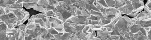
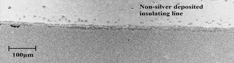


9 Selective Ag electroplating on epitaxial REBCO in between inkjet printed insulator stripes 9


10 Lowered ac losses in filamentized conductor made with no material removal 10-fold reduction in ac loss in 12-filament conductor made with no material removal 10


11 Fully-filamentized conductor by mechanical scribing and selective electroplating REBCO Buffer Stack Oxide Layer Ag Hastelloy Hastelloy Electroplated Cu Mechanical Scribing + oxygenation Selective Cu Electroplating Non-striated 12-filament, 12 mm wide Ag 12 mm wide sputtered tape tape 12-filament tape with electroplated l t Cu Mechanical Scribing Oxygenation + ED Cu 11
12 Significant ac loss reduction in full-filamentized conductor with copper stabilizer Critical current of standard 16 conductor = 207 A Critical current of 12-filament 12 conductor = 197 A 10 W/m) ac loss ( Critical current of 12-filament conductor after 10 µm copper 6 stabilizer = 200 A 4 AC loss of 12-fiament conductor at 60 Hz is 11 times lower than that of unstriated conductor without copper stabilizer and 13 times lower with copper stabilizer, at higher fields T 0.02 Multfilamentary Standard Multfilamentary + Cu Standard + Cu ac field frequency (Hz)


13 Investigated selectively electroplated copper thickness & coupling effects S1 S2 S3 S4 S5 S6 ~10 µm ~20 µm ~30 µm ~44 µm ~36 µm ~33 µm Fully coupled Mechanically scribed, no oxidation and Cu plated No filamentization 13


 14")
14 Sideways growth of electroplated copper reduces groove width between filaments S1 Groove Oxide Filament Copper S3 Groove Oxide Filament Copper 40 µm Filament Copper 15 µm No coupling Mechanically scribed, oxidized and Cu plated (~ 10 µm) No coupling Mechanically scribed, oxidized and Cu plated (~ 30 µm) 14


15 Partially and fully-coupled filamentized tape with copper stabilizer S4 S5 Filament Copper Groove partial Cu Groove Copper Filament Copper Partially coupled Mechanically scribed, oxidized and Cu plated (~ 44 µm) Fully coupled Mechanically scribed, no oxidation and Cu plated (~ 33 µm) 15

16 No significant loss contribution up to 30 µm stabilizer in fully-filamentized conductor at 40 Hz 40 Hz Non-striated B-I with Ic=195 A Striated B-I with Ic=195 A 15-fold ac loss reduction even with 30 µm Cu stabilizer Lower ac loss reduction with 40 µm Cu stabilizer 16
17 No significant loss contribution up to 30 µm stabilizer in fully-filamentized conductor even at 400 Hz 400 Hz 17


18 15-fold ac loss reduction in fully-filamentized conductor with up to 30 µm stabilizer ~15 times 40 Hz Magnetic Electrical Coupling + eddy current Reduction is still more than 12-fold but decreases in 400 Hz (heating effects) Loss ratio: ac loss of filamentized conductor S3/ac loss of non-striated conductor S6 18


19 5-fold ac loss reduction at 40 Hz even in partially-coupled filamentized conductor with 44 µm stabilizer Magnetic Almost 5 times 40 Hz Electrical Coupling + eddy current Striation becomes ineffective at 400 Hz Loss ratio: ac loss of filamentized conductor S4/ac loss of non-striated conductor S6 19


20 Fully-coupled filamentized conductor with 36 µm stabilizer shows comparable ac loss at 40 Hz and higher loss at 400 Hz Weak effect of 40 Hz Electrical Coupling Striation 400 Hz Losses increases beyond S6 due to Magnetic + Electrical coupling Loss ratio: ac loss of filamentized conductor S5/ac loss of non-striated conductor S6 20
21 Summary Selective electroplating has been proven to achieve fully-filamentized coated conductor even with thick copper stabilizer. Coated conductor with up to 30 µm copper stabilizer can be fully-filamentized without any coupling. 15-fold ac loss reduction achieved compared to reference non-striated coated conductor with ~ 30 µm copper stabilizer Coated conductor with 40 µm copper stabilizer can be fully-filamentized with partial coupling (due to sideways growth of copper across groove) 5-fold ac loss reduction achieved at 40 Hz even with partial coupling compared to reference non-striated coated conductor Fully-filamentized coated conductor with no coupling can be achieved even with thicker copper stabilizer using wider grooves Fully-coupled filamentized conductor (conductive material in groove) shows higher ac loss than non-striated conductor: in this case striation makes the situation worse! 21
Recent Results in 2G HTS Wire Technology Development at SuperPower
 superior performance. powerful technology. Recent Results in 2G HTS Wire Technology Development at SuperPower J. Jimenez, Y. Chen, X. Xiong, Y. Xie, X. Zhang, A. Rar, M. Martchevskii, Y. Qiao, A.Knoll,
Exploration of Pinhole and Defect Density in Insulating Layer of Magnetic Tunnel Junctions
 Exploration of Pinhole and Defect Density in Insulating Layer of Magnetic Tunnel Junctions Rainer Schad, Drew Allen, Kether Mayen Giovanni Zangari, Iulica Zana, Dehua Yang University of Alabama Mark Tondra,
Meeting customer requirements for ROEBEL cable for ac applications
 Meeting customer requirements for ROEBEL cable for ac applications ROEBEL cable is a known approach to produce low ac loss, high current conductor/cable Conductor exposed to severe mechanical cutting at
DC and AC Characterization of Pancake Coils Made from Roebel-Assembled Coated Conductor Cable
 DC and AC Characterization of Pancake Coils Made from Roebel-Assembled Coated Conductor Cable 1 Anna Kario, Michal Vojenčiak, Francesco Grilli, Andrea Kling, Alexandra Jung, Jörg Brand, Andrej Kudymow,
On-chip 3D air core micro-inductor for high-frequency applications using deformation of sacrificial polymer
 header for SPIE use On-chip 3D air core micro-inductor for high-frequency applications using deformation of sacrificial polymer Nimit Chomnawang and Jeong-Bong Lee Department of Electrical and Computer
Microfabrication technologies for highly-laminated thick metallic cores and 3-D integrated windings
 Microfabrication technologies for highly-laminated thick metallic cores and 3-D integrated windings Florian Herrault Georgia Institute of Technology Atlanta, GA florian@gatech.edu http://mems.gatech.edu/msma
INF 5490 RF MEMS. LN12: RF MEMS inductors. Spring 2011, Oddvar Søråsen Department of informatics, UoO
 INF 5490 RF MEMS LN12: RF MEMS inductors Spring 2011, Oddvar Søråsen Department of informatics, UoO 1 Today s lecture What is an inductor? MEMS -implemented inductors Modeling Different types of RF MEMS
Wirelessly powered micro-tracer enabled by miniaturized antenna and microfluidic channel
 Journal of Physics: Conference Series PAPER OPEN ACCESS Wirelessly powered micro-tracer enabled by miniaturized antenna and microfluidic channel To cite this article: G Duan et al 2015 J. Phys.: Conf.
(a) (d) (e) (b) (c) (f) 3D-NAND Flash and Its Manufacturing Process
 (d) (e) (b) (c) (f) 3D-NAND Flash and Its Manufacturing Process") 3D-NAND Flash and Its Manufacturing Process 79 (d) Si Si (b) (c) (e) Si (f) +1-2 (g) (h) Figure 2.33 Top-down view in cap oxide and (b) in nitride_n-2; (c) cross-section near the top of the channel; top-down
3D-NAND Flash and Its Manufacturing Process 79 (d) Si Si (b) (c) (e) Si (f) +1-2 (g) (h) Figure 2.33 Top-down view in cap oxide and (b) in nitride_n-2; (c) cross-section near the top of the channel; top-down
Micro-inductors integrated on silicon for power supply on chip
 Journal of Magnetism and Magnetic Materials 316 (27) e233 e237 www.elsevier.com/locate/jmmm Micro-inductors integrated on silicon for power supply on chip Ningning Wang, Terence O Donnell, Saibal Roy,
Update on REBCO accelerator magnet technology development at LBNL and research plan for fusion magnets
 Update on REBCO accelerator magnet technology development at LBNL and research plan for fusion magnets Xiaorong Wang Superconducting Magnet Program, LBNL CCA Workshop, Aspen CO, 9/12/2016 Acknowledgment
Sub-cooled SFCL Device and Modules for Power Transmission / Distribution
 superior performance. powerful technology. Sub-cooled SFCL Device and Modules for Power Transmission / Distribution Juan-Carlos H. Llambes, Ph.D. SFCL Program Manager / Senior High Voltage Engineer University
A Low-cost Through Via Interconnection for ISM WLP
 A Low-cost Through Via Interconnection for ISM WLP Jingli Yuan, Won-Kyu Jeung, Chang-Hyun Lim, Seung-Wook Park, Young-Do Kweon, Sung Yi To cite this version: Jingli Yuan, Won-Kyu Jeung, Chang-Hyun Lim,
Microtools Shaped by Focused Ion Beam Milling and the Fabrication of Cylindrical Coils
 Microtools Shaped by Focused Ion Beam Milling and the Fabrication of Cylindrical Coils M.J. Vasile, D.P. Adams #, and Y.N. Picard* Sandia National Laboratories P.O. Box 5800, MS 0959 Albuquerque, NM, 87185
Fabrication and application of a wireless inductance-capacitance coupling microsensor with electroplated high permeability material NiFe
 Journal of Physics: Conference Series Fabrication and application of a wireless inductance-capacitance coupling microsensor with electroplated high permeability material NiFe To cite this article: Y H
Integrated Circuits: FABRICATION & CHARACTERISTICS - 4. Riju C Issac
 Integrated Circuits: FABRICATION & CHARACTERISTICS - 4 Riju C Issac INTEGRATED RESISTORS Resistor in a monolithic IC is very often obtained by the bulk resistivity of one of the diffused areas. P-type
TECHNICAL REPORT: CVEL Parasitic Inductance Cancellation for Filtering to Chassis Ground Using Surface Mount Capacitors
 TECHNICAL REPORT: CVEL-14-059 Parasitic Inductance Cancellation for Filtering to Chassis Ground Using Surface Mount Capacitors Andrew J. McDowell and Dr. Todd H. Hubing Clemson University April 30, 2014
Nanofluidic Diodes based on Nanotube Heterojunctions
 Supporting Information Nanofluidic Diodes based on Nanotube Heterojunctions Ruoxue Yan, Wenjie Liang, Rong Fan, Peidong Yang 1 Department of Chemistry, University of California, Berkeley, CA 94720, USA
The Superconducting Strand for the CMS Solenoid Conductor
 The Superconducting Strand for the CMS Solenoid Conductor B. Curé, B. Blau, D. Campi, L. F. Goodrich, I. L. Horvath, F. Kircher, R. Liikamaa, J. Seppälä, R. P. Smith, J. Teuho, and L. Vieillard Abstract-
A new class of LC-resonator for micro-magnetic sensor application
 Journal of Magnetism and Magnetic Materials 34 (26) 117 121 www.elsevier.com/locate/jmmm A new class of LC-resonator for micro-magnetic sensor application Yong-Seok Kim a, Seong-Cho Yu a, Jeong-Bong Lee
Deliverable 3.1 Passive Components Fabrication
 PowerSWIPE (Project no. 318529) POWER SoC With Integrated PassivEs Deliverable 3.1 Passive Components Fabrication Dissemination level: PU Responsible Beneficiary Tyndall National Institute, University
Vol. 58 No. 7. July MVP NI AWR Design Environment. Founded in 1958
 Vol. 58 No. 7 July 215.com MVP NI AWR Design Environment Founded in 1958 98 MICROWAVE JOURNAL JULY 215 Managing Circuit Materials at mmwave Frequencies John Coonrod Rogers Corp., Chandler, Ariz. This article
Integrated diodes. The forward voltage drop only slightly depends on the forward current. ELEKTRONIKOS ĮTAISAI
 1 Integrated diodes pn junctions of transistor structures can be used as integrated diodes. The choice of the junction is limited by the considerations of switching speed and breakdown voltage. The forward
Design and Fabrication of On-Chip Inductors. Q = 2~ at a resonance frequency
 Design and Fabrication of On-Chip Inductors Robert K. Requa Microelectronic Engineering Rochester Institute of Technology Rochester, NY 14623 Abstract-- An inductor is a conductor arranged in an appropriate
High Performance Silicon-Based Inductors for RF Integrated Passive Devices
 Progress In Electromagnetics Research, Vol. 146, 181 186, 2014 High Performance Silicon-Based Inductors for RF Integrated Passive Devices Mei Han, Gaowei Xu, and Le Luo * Abstract High-Q inductors are
Topic 3. CMOS Fabrication Process
 Topic 3 CMOS Fabrication Process Peter Cheung Department of Electrical & Electronic Engineering Imperial College London URL: www.ee.ic.ac.uk/pcheung/ E-mail: p.cheung@ic.ac.uk Lecture 3-1 Layout of a Inverter
Inductors In Silicon Based on SU-8 Enhanced Silicon Molding Technique for Portable Electronics
 Biophotonics & Microsystems Lab Inductors In Silicon Based on SU-8 Enhanced Silicon Molding Technique for Portable Electronics Mingliang Wang 1*, Khai D. T. Ngo 2, Huikai Xie 1 1 BML, University of Florida
Chapter 3 Fabrication
 Chapter 3 Fabrication The total structure of MO pick-up contains four parts: 1. A sub-micro aperture underneath the SIL The sub-micro aperture is used to limit the final spot size from 300nm to 600nm for
EMI Shielding and Grounding Materials
 EMI Shielding and Grounding Materials P-SHIELD Shielding and Grounding Materials Polymer Science, Inc. offers a complete EMI shielding and grounding materials product line. P-SHIELD EMI shielding materials
The Effects of PCB Fabrication on High-Frequency Electrical Performance
 The Effects of PCB Fabrication on High-Frequency Electrical Performance John Coonrod, Rogers Corporation Advanced Circuit Materials Division Achieving optimum high-frequency printed-circuit-board (PCB)
By Hannah Perner-Wilson.
 By Hannah Perner-Wilson www.kit-of-no-parts.at Submitted to the Program in Media Arts and Sciences, School of Architecture and Planning, in partial fulfilment of the requirements for the degree of Masters
y y (12) Patent Application Publication (10) Pub. No.: US 2015/ A1 (19) United States (43) Pub. Date: Sep. 10, C 410C 422b 4200
 Patent Application Publication (10) Pub. No.: US 2015/ A1 (19) United States (43) Pub. Date: Sep. 10, C 410C 422b 4200") (19) United States (12) Patent Application Publication (10) Pub. No.: US 2015/0255300 A1 He et al. US 201502553.00A1 (43) Pub. Date: Sep. 10, 2015 (54) (71) (72) (73) (21) (22) DENSELY SPACED FINS FOR
(19) United States (12) Patent Application Publication (10) Pub. No.: US 2015/0255300 A1 He et al. US 201502553.00A1 (43) Pub. Date: Sep. 10, 2015 (54) (71) (72) (73) (21) (22) DENSELY SPACED FINS FOR
World record DC (45.5 T) magnetic field using a REBCO insert inside a 31 T resistive magnet
 magnetic field using a REBCO insert inside a 31 T resistive magnet") World record DC (45.5 T) magnetic field using a REBCO insert inside a 31 T resistive magnet Seungyong Hahn1, Kwanglok Kim, Kwangmin Kim, Xinbo Hu, Thomas Painter, Iain Dixon, Seokho Kim2, Kabindra Bhattarai,
World record DC (45.5 T) magnetic field using a REBCO insert inside a 31 T resistive magnet Seungyong Hahn1, Kwanglok Kim, Kwangmin Kim, Xinbo Hu, Thomas Painter, Iain Dixon, Seokho Kim2, Kabindra Bhattarai,
This writeup is adapted from Fall 2002, final project report for by Robert Winsor.
 Optical Waveguides in Andreas G. Andreou This writeup is adapted from Fall 2002, final project report for 520.773 by Robert Winsor. September, 2003 ABSTRACT This lab course is intended to give students
MOSFET & IC Basics - GATE Problems (Part - I)
") MOSFET & IC Basics - GATE Problems (Part - I) 1. Channel current is reduced on application of a more positive voltage to the GATE of the depletion mode n channel MOSFET. (True/False) [GATE 1994: 1 Mark]
MOSFET & IC Basics - GATE Problems (Part - I) 1. Channel current is reduced on application of a more positive voltage to the GATE of the depletion mode n channel MOSFET. (True/False) [GATE 1994: 1 Mark]
EE 330 Lecture 7. Design Rules. IC Fabrication Technology Part 1
 EE 330 Lecture 7 Design Rules IC Fabrication Technology Part 1 Review from Last Time Technology Files Provide Information About Process Process Flow (Fabrication Technology) Model Parameters Design Rules
On-Chip Passive Devices Embedded in Wafer-Level Package
 On-Chip Passive Devices Embedded in Wafer-Level Package Kazuya Masu 1, Kenichi Okada 1, Kazuhisa Itoi 2, Masakazu Sato 2, Takuya Aizawa 2 and Tatsuya Ito 2 On-chip high-q spiral and solenoid inductors
Layout of a Inverter. Topic 3. CMOS Fabrication Process. The CMOS Process - photolithography (2) The CMOS Process - photolithography (1) v o.
 The CMOS Process - photolithography (1) v o.") Layout of a Inverter Topic 3 CMOS Fabrication Process V DD Q p Peter Cheung Department of Electrical & Electronic Engineering Imperial College London v i v o Q n URL: www.ee.ic.ac.uk/pcheung/ E-mail: p.cheung@ic.ac.uk
Layout of a Inverter Topic 3 CMOS Fabrication Process V DD Q p Peter Cheung Department of Electrical & Electronic Engineering Imperial College London v i v o Q n URL: www.ee.ic.ac.uk/pcheung/ E-mail: p.cheung@ic.ac.uk
Integrated Electroplated Micromachined Magnetic Devices Using Low Temperature Fabrication Processes
 48 IEEE TRANSACTIONS ON ELECTRONICS PACKAGING MANUFACTURING, VOL. 23, NO. 1, JANUARY 2000 Integrated Electroplated Micromachined Magnetic Devices Using Low Temperature Fabrication Processes Jae Yeong Park,
CMOS Digital Integrated Circuits Lec 2 Fabrication of MOSFETs
 CMOS Digital Integrated Circuits Lec 2 Fabrication of MOSFETs 1 CMOS Digital Integrated Circuits 3 rd Edition Categories of Materials Materials can be categorized into three main groups regarding their
Conference Paper Cantilever Beam Metal-Contact MEMS Switch
 Conference Papers in Engineering Volume 2013, Article ID 265709, 4 pages http://dx.doi.org/10.1155/2013/265709 Conference Paper Cantilever Beam Metal-Contact MEMS Switch Adel Saad Emhemmed and Abdulmagid
PAGE 1/6 ISSUE Jul SERIES Micro-SPDT PART NUMBER R516 XXX 10X R 516 _ 1 0 _
 PAGE 1/6 ISSUE Jul-24-2017 SERIES Micro-SPDT PART NUMBER R516 XXX 10X R516 series: the RAMSES concept merges with the SLIM LINE technology, breaking up the frequency limits of SMT switches : - FULL SMT
Flexible Substrates and SCB-Technology
 Flexible Substrates and SCB-Technology Substrate Technology As requirements are increasing, so are electronic systems becoming smaller and smaller and more complex. In its role as innovative forerunner
Precision microcomb design and fabrication for x-ray optics assembly
 Precision microcomb design and fabrication for x-ray optics assembly Yanxia Sun, a) Ralf K. Heilmann, b) Carl G. Chen, Craig R. Forest, and Mark L. Schattenburg Space Nanotechnology Laboratory, Center
Hermetic Packaging Solutions using Borosilicate Glass Thin Films. Lithoglas Hermetic Packaging Solutions using Borosilicate Glass Thin Films
 Hermetic Packaging Solutions using Borosilicate Glass Thin Films 1 Company Profile Company founded in 2006 ISO 9001:2008 qualified since 2011 Headquarters and Production in Dresden, Germany Production
Final Report. Superconducting Coils for AC currents Using YBCO Coated Conductors
 Institute of Electrical Engineering Slovak Academy of Sciences 841 04 Bratislava, Dúbravská cesta 9, Slovak Republic Final Report Superconducting Coils for AC currents Using YBCO Coated Conductors Award
Advanced High-Density Interconnection Technology
 Advanced High-Density Interconnection Technology Osamu Nakao 1 This report introduces Fujikura s all-polyimide IVH (interstitial Via Hole)-multi-layer circuit boards and device-embedding technology. Employing
Performance Enhancement For Spiral Indcutors, Design And Modeling
 Performance Enhancement For Spiral Indcutors, Design And Modeling Mohammad Hossein Nemati 16311 Sabanci University Final Report for Semiconductor Process course Introduction: How to practically improve
Optimization of Layer Thickness to Yield Predetermined Shielding Performance of Multilayer Conductor Electromagnetic Shield
 Optimization of Layer Thickness to Yield Predetermined Shielding Performance of Multilayer Conductor Electromagnetic Shield C Dharma Raj D Vijaya Saradhi P Hemambaradhara Rao P Chandra Sekhar GITAM University
RF/MICROWAVE HYBRIDS Basics, Materials and Processes
 RF/MICROWAVE HYBRIDS Basics, Materials and Processes RF/MICROWAVE HYBRIDS Basics, Materials and Processes by Richard Brown Richard Brown Associates, Inc. Shelton, CT KLUWER ACADEMIC PUBLISHERS NEW YORK,
IN HIGHLY efficient high-current devices, such as electromagnetic
 JOURNAL OF MICROELECTROMECHANICAL SYSTEMS, VOL. 19, NO. 6, DECEMBER 2010 1277 Parylene-Insulated Ultradense Microfabricated Coils Florian Herrault, Svyatoslav Yorish, Thomas M. Crittenden, Chang-Hyeon
Fabrication of a DRAM Cube Using a Novel Laser Patterned 3-D Interconnect Process
 UCRL-JC-125631 PREPRINT Fabrication of a DRAM Cube Using a Novel Laser Patterned 3-D Interconnect Process V. Malba V. Liberman A.F. Bernhardt This paper was prepared for submittal to the International
2 Single-mode Diode Laser and Optical Fiber
 A Novel Technique for Minimum Quench Energy Measurements in Superconductors Using a Single-Mode Diode Laser F. Trillaud (a), F. Ayela (b), A. Devred (a),(c), M. Fratini (d), D. Lebœuf (a) and P. Tixador
This is the accepted version of a paper presented at 2018 IEEE/MTT-S International Microwave Symposium - IMS, Philadelphia, PA, June 2018.
 http://www.diva-portal.org Postprint This is the accepted version of a paper presented at 2018 IEEE/MTT-S International Microwave Symposium - IMS, Philadelphia, PA, 10-15 June 2018. Citation for the original
Flip Chips. FA10-200x200 FA10-400x400 FA10-600x x 200 mils 400 x 400 mils
 Flip Chip FlipChip International Flip Chip describes the method of electrically connecting the die to the package carrier. The package carrier, either substrate or leadframe, then provides the connection
Wafer-scale 3D integration of silicon-on-insulator RF amplifiers
 Wafer-scale integration of silicon-on-insulator RF amplifiers The MIT Faculty has made this article openly available. Please share how this access benefits you. Your story matters. Citation As Published
IMAGING SILICON NANOWIRES
 Project report IMAGING SILICON NANOWIRES PHY564 Submitted by: 1 Abstract: Silicon nanowires can be easily integrated with conventional electronics. Silicon nanowires can be prepared with single-crystal
Key Questions. ECE 340 Lecture 39 : Introduction to the BJT-II 4/28/14. Class Outline: Fabrication of BJTs BJT Operation
 Things you should know when you leave ECE 340 Lecture 39 : Introduction to the BJT-II Fabrication of BJTs Class Outline: Key Questions What elements make up the base current? What do the carrier distributions
High-yield Fabrication Methods for MEMS Tilt Mirror Array for Optical Switches
 : MEMS Device Technologies High-yield Fabrication Methods for MEMS Tilt Mirror Array for Optical Switches Joji Yamaguchi, Tomomi Sakata, Nobuhiro Shimoyama, Hiromu Ishii, Fusao Shimokawa, and Tsuyoshi
IEEE/CSC & ESAS SUPERCONDUCTIVITY NEWS FORUM
 Kryo 2013 Modern AC Josephson voltage standards at PTB J. Kohlmann, F. Müller, O. Kieler, Th. Scheller, R. Wendisch, B. Egeling, L. Palafox, J. Lee, and R. Behr Physikalisch-Technische Bundesanstalt Φ
RESISTANCE IN WIRES 4) 4R
 4R") RESISTANCE IN WIRES NAME: 1. A copper wire of length L and cross-sectional area A has resistance R. A second copper wire at the same temperature has a length of 2L and a cross-sectional area of 1 2A. What
RESISTANCE IN WIRES NAME: 1. A copper wire of length L and cross-sectional area A has resistance R. A second copper wire at the same temperature has a length of 2L and a cross-sectional area of 1 2A. What
Quasi-Phase-Matched Faraday Rotation in Semiconductor Waveguides with a Magneto-Optic Cladding for Monolithically Integrated Optical Isolators
 Quasi-Phase-Matched Faraday Rotation in Semiconductor Waveguides with a Magneto-Optic Cladding for Monolithically Integrated Optical Isolators Prof. David C. Hutchings, Barry M. Holmes and Cui Zhang, Acknowledgements
Measurement and noise performance of nano-superconducting-quantuminterference devices fabricated by focused ion beam
 Measurement and noise performance of nano-superconducting-quantuminterference devices fabricated by focused ion beam L. Hao,1,a_ J. C. Macfarlane,1 J. C. Gallop,1 D. Cox,1 J. Beyer,2 D. Drung,2 and T.
Modeling, Design, and Demonstration of 2.5D Glass Interposers for 16-Channel 28 Gbps Signaling Applications
 Modeling, Design, and Demonstration of 2.5D Glass Interposers for 16-Channel 28 Gbps Signaling Applications Brett Sawyer, Bruce C. Chou, Saumya Gandhi, Jack Mateosky, Venky Sundaram, and Rao Tummala 3D
Magnetic and Electromagnetic Microsystems. 4. Example: magnetic read/write head
 Magnetic and Electromagnetic Microsystems 1. Magnetic Sensors 2. Magnetic Actuators 3. Electromagnetic Sensors 4. Example: magnetic read/write head (C) Andrei Sazonov 2005, 2006 1 Magnetic microsystems
PAGE 1/6 ISSUE SERIES Micro-SPDT PART NUMBER R516 XXX 10X. (All dimensions are in mm [inches]) R 516 _ 1 0 _
![PAGE 1/6 ISSUE SERIES Micro-SPDT PART NUMBER R516 XXX 10X. (All dimensions are in mm [inches]) R 516 _ 1 0 _](/thumbs/96/127769340.jpg "PAGE 1/6 ISSUE SERIES Micro-SPDT PART NUMBER R516 XXX 10X. (All dimensions are in mm [inches]) R 516 _ 1 0 _") PAGE 1/6 ISSUE 15-10-18 SERIES Micro-SPDT PART NUMBER R516 XXX 10X R516 series: the RAMSES concept merges with the SLIM LINE technology, breaking up the frequency limits of SMT switches : - FULL SMT TECHNOLOGY
PAGE 1/6 ISSUE 15-10-18 SERIES Micro-SPDT PART NUMBER R516 XXX 10X R516 series: the RAMSES concept merges with the SLIM LINE technology, breaking up the frequency limits of SMT switches : - FULL SMT TECHNOLOGY
FEM SIMULATION FOR DESIGN AND EVALUATION OF AN EDDY CURRENT MICROSENSOR
 FEM SIMULATION FOR DESIGN AND EVALUATION OF AN EDDY CURRENT MICROSENSOR Heri Iswahjudi and Hans H. Gatzen Institute for Microtechnology Hanover University Callinstrasse 30A, 30167 Hanover Germany E-mail:
Ion Assisted Deposition Processes for Precision and Laser Optics
 Ion Assisted Deposition Processes for Precision and Laser Optics H. Ehlers, T. Groß, M. Lappschies, and D. Ristau Laser Zentrum Hannover e.v. Germany Introduction Ion assisted deposition (IAD) processes
ECE 5745 Complex Digital ASIC Design Topic 2: CMOS Devices
 ECE 5745 Complex Digital ASIC Design Topic 2: CMOS Devices Christopher Batten School of Electrical and Computer Engineering Cornell University http://www.csl.cornell.edu/courses/ece5950 Simple Transistor
Through Glass Via (TGV) Technology for RF Applications
 Technology for RF Applications") Through Glass Via (TGV) Technology for RF Applications C. H. Yun 1, S. Kuramochi 2, and A. B. Shorey 3 1 Qualcomm Technologies, Inc. 5775 Morehouse Dr., San Diego, California 92121, USA Ph: +1-858-651-5449,
Through Glass Via (TGV) Technology for RF Applications C. H. Yun 1, S. Kuramochi 2, and A. B. Shorey 3 1 Qualcomm Technologies, Inc. 5775 Morehouse Dr., San Diego, California 92121, USA Ph: +1-858-651-5449,
Supporting Information. A Tough and High-Performance Transparent Electrode from a. Scalable Transfer-Free Method
 Supporting Information A Tough and High-Performance Transparent Electrode from a Scalable Transfer-Free Method Tianda He, Aozhen Xie, Darrell H. Reneker and Yu Zhu * Department of Polymer Science, College
Supplementary Information
 Supplementary Information Wireless thin film transistor based on micro magnetic induction coupling antenna Byoung Ok Jun 1, Gwang Jun Lee 1, Jong Gu Kang 1,2, Seung Uk Kim 1, Ji Woong Choi 1, Seung Nam
Semiconductor Physics and Devices
 Metal-Semiconductor and Semiconductor Heterojunctions The Metal-Oxide-Semiconductor Field-Effect Transistor (MOSFET) is one of two major types of transistors. The MOSFET is used in digital circuit, because
Analysis of Superconducting Fault Current Limiter in DC System with Renewable Energy Sources
 International Journal of Electrical Engineering. ISSN 0974-2158 Volume 8, Number 4 (2015), pp. 329-339 International Research Publication House http://www.irphouse.com Analysis of Superconducting Fault
Design and Analysis of 28 GHz Millimeter Wave Antenna Array for 5G Communication Systems
 Journal of Science Technology Engineering and Management-Advanced Research & Innovation ISSN 2581-4982 Vol. 1, Issue 3, August 2018 Design and Analysis of 28 GHz Millimeter Wave Antenna Array for 5G Communication
The Effects of PCB Fabrication on High-Frequency Electrical Performance
 As originally published in the IPC APEX EXPO Conference Proceedings. The Effects of PCB Fabrication on High-Frequency Electrical Performance John Coonrod, Rogers Corporation Advanced Circuit Materials
An X band RF MEMS switch based on silicon-on-glass architecture
 Sādhanā Vol. 34, Part 4, August 2009, pp. 625 631. Printed in India An X band RF MEMS switch based on silicon-on-glass architecture M S GIRIDHAR, ASHWINI JAMBHALIKAR, J JOHN, R ISLAM, C L NAGENDRA and
Outline. 1 Introduction. 2 Basic IC fabrication processes. 3 Fabrication techniques for MEMS. 4 Applications. 5 Mechanics issues on MEMS MDL NTHU
 Outline 1 Introduction 2 Basic IC fabrication processes 3 Fabrication techniques for MEMS 4 Applications 5 Mechanics issues on MEMS 2.2 Lithography Reading: Runyan Chap. 5, or 莊達人 Chap. 7, or Wolf and
High-efficiency, high-speed VCSELs with deep oxidation layers
 Manuscript for Review High-efficiency, high-speed VCSELs with deep oxidation layers Journal: Manuscript ID: Manuscript Type: Date Submitted by the Author: Complete List of Authors: Keywords: Electronics
NUMERICAL MODEL OF THE 10 KVA TRANSFORMER WITH COPPER WINDINGS
 Maszyny Elektryczne - Zeszyty Problemowe Nr 3/2017 (115) 77 Łukasz Woźniak, Leszek Jaroszyński, Paweł Surdacki Lublin University of Technology NUMERICAL MODEL OF THE 10 KVA TRANSFORMER WITH COPPER WINDINGS
CITY UNIVERSITY OF HONG KONG
 CITY UNIVERSITY OF HONG KONG Modeling and Analysis of the Planar Spiral Inductor Including the Effect of Magnetic-Conductive Electromagnetic Shields Submitted to Department of Electronic Engineering in
Aerosol-Jet Printed Quasi-Optical Terahertz Filters
 2017 IEEE 67th Electronic Components and Technology Conference Aerosol-Jet Printed Quasi-Optical Terahertz Filters Christopher Oakley, Amanpreet Kaur, Jennifer A. Byford, and Premjeet Chahal Michigan State
Electrostatically Tunable Analog Single Crystal Silicon Fringing-Field MEMS Varactors
 Purdue University Purdue e-pubs Birck and NCN Publications Birck Nanotechnology Center 2009 Electrostatically Tunable Analog Single Crystal Silicon Fringing-Field MEMS Varactors Joshua A. Small Purdue
Inkjet Filling of TSVs with Silver Nanoparticle Ink. Behnam Khorramdel, Matti Mäntysalo Tampere University of Technology ESTC 2014 Finland, Helsinki
 Inkjet Filling of TSVs with Silver Nanoparticle Ink Behnam Khorramdel, Matti Mäntysalo Tampere University of Technology ESTC 2014 Finland, Helsinki Outline Motivation for this study Inkjet in MEMS fabrication
Electrothermal Actuator
 Electrothermal Actuator 09-09-14 Generated by CleanRoom Substrate thickness: 50 (µm) Comments: 1. Substrate Si Czochralski (100) Film Thickness: 600 nm (Conformal) Comments: 2. Deposition Si3N4 PECVD (Ar)
Motivation Different Strategies for Induction integration. Package-Integrated VR with Intel Core 2 Duo Processor. ! Thru-Silicon-Vias (TSV) in future
 in future") Optimization of soft magnetic thin films structures in on-chip inductors for Hao Wu, Donald S. Gardner, and Hongbin Yu Ira A. Fulton Schools of Engineering, Arizona State University, Tempe, AZ8587, United
Optimization of soft magnetic thin films structures in on-chip inductors for Hao Wu, Donald S. Gardner, and Hongbin Yu Ira A. Fulton Schools of Engineering, Arizona State University, Tempe, AZ8587, United
Optical Bus for Intra and Inter-chip Optical Interconnects
 Optical Bus for Intra and Inter-chip Optical Interconnects Xiaolong Wang Omega Optics Inc., Austin, TX Ray T. Chen University of Texas at Austin, Austin, TX Outline Perspective of Optical Backplane Bus
2.3 PF System. WU Weiyue PF5 PF PF1
 2.3 PF System WU Weiyue 2.3.1 Introduction The poloidal field (PF) system consists of fourteen superconducting coils, including 6 pieces of central selenoid coils, 4 pieces of divertor coils and 4 pieces
Development of CORC cables for helium gas cooled power transmission and fault current limiting applications
 Superconductor Science and Technology Supercond. Sci. Technol. 31 (2018) 085011 (10pp) https://doi.org/10.1088/1361-6668/aacf6b Development of CORC cables for helium gas cooled power transmission and fault
Machine-Aligned Fabrication of Submicron SIS Tunnel Junctions Using a Focused Ion Beam
 Machine-Aligned Fabrication of Submicron SIS Tunnel Junctions Using a Focused Ion Beam Robert. B. Bass, Jian. Z. Zhang and Aurthur. W. Lichtenberger Department of Electrical Engineering, University of
Low-power carbon nanotube-based integrated circuits that can be transferred to biological surfaces
 SUPPLEMENTARY INFORMATION Articles https://doi.org/10.1038/s41928-018-0056-6 In the format provided by the authors and unedited. Low-power carbon nanotube-based integrated circuits that can be transferred
Processes for Flexible Electronic Systems
 Processes for Flexible Electronic Systems Michael Feil Fraunhofer Institut feil@izm-m.fraunhofer.de Outline Introduction Single sheet versus reel-to-reel (R2R) Substrate materials R2R printing processes
420 Intro to VLSI Design
 Dept of Electrical and Computer Engineering 420 Intro to VLSI Design Lecture 0: Course Introduction and Overview Valencia M. Joyner Spring 2005 Getting Started Syllabus About the Instructor Labs, Problem
TCLAD: TOOLS FOR AN OPTIMAL DESIGN
 TCLAD: TOOLS FOR AN OPTIMAL DESIGN THINGS TO CONSIDER WHEN DESIGNING CIRCUITS Many factors come into play in circuit design with respect to etching, surface finishing and mechanical fabrication processes;
MICROSTRUCTURING OF METALLIC LAYERS FOR SENSOR APPLICATIONS
 MICROSTRUCTURING OF METALLIC LAYERS FOR SENSOR APPLICATIONS Vladimír KOLAŘÍK, Stanislav KRÁTKÝ, Michal URBÁNEK, Milan MATĚJKA, Jana CHLUMSKÁ, Miroslav HORÁČEK, Institute of Scientific Instruments of the
Nano Josephson Superconducting Tunnel Junctions in Y-Ba-Cu-O Direct- Patterned with a Focused Helium Ion Beam
 Nano Josephson Superconducting Tunnel Junctions in Y-Ba-Cu-O Direct- Patterned with a Focused Helium Ion Beam Authors: Shane A. Cybart, 1,2,* E. Y. Cho, 1 T. J. Wong, 1 Björn H. Wehlin, 1 Meng K. Ma, 1
DIY fabrication of microstructures by projection photolithography
 DIY fabrication of microstructures by projection photolithography Andrew Zonenberg Rensselaer Polytechnic Institute 110 8th Street Troy, New York U.S.A. 12180 zonena@cs.rpi.edu April 20, 2011 Abstract
Enabling Resonant Clock Distribution with Scaled On-Chip Magnetic Inductors
 Enabling Resonant Clock Distribution with Scaled On-Chip Magnetic Inductors Saurabh Sinha, Wei Xu, Jyothi B. Velamala, Tawab Dastagir, Bertan Bakkaloglu, Hongbin Yu and Yu Cao Department of Electrical
Photolithography I ( Part 1 )
") 1 Photolithography I ( Part 1 ) Chapter 13 : Semiconductor Manufacturing Technology by M. Quirk & J. Serda Bjørn-Ove Fimland, Department of Electronics and Telecommunication, Norwegian University of Science
1 Photolithography I ( Part 1 ) Chapter 13 : Semiconductor Manufacturing Technology by M. Quirk & J. Serda Bjørn-Ove Fimland, Department of Electronics and Telecommunication, Norwegian University of Science
Ultra-thin, highly flexible RF cables and interconnections
 Ultra-thin, highly flexible RF cables and interconnections Hans Burkard, Hightec MC AG, Lenzburg, Switzerland Urs Brunner, Hightec MC AG, Lenzburg, Switzerland Karl Kurz, Hightec MC AG, Lenzburg, Switzerland