More Imaging Luc De Mey - CEO - CMOSIS SA
|
|
|
- Diana Douglas
- 6 years ago
- Views:
Transcription

1 More Imaging Luc De Mey - CEO - CMOSIS SA Annual Review / June 28, 2011
2 More Imaging CMOSIS: Vision & Mission CMOSIS s Business Concept On-Going R&D: More Imaging
3 CMOSIS s Vision Image capture is a key technology with ever growing number of applications. Specific imaging applications require specific and optimized Image Sensors.
4 CMOSIS s Mission Be a leading supplier of Image Sensors optimized for Industrial, Professional and Scientific Applications.
5 CMOSIS s Business Model Development, Qualification, Production and Supply of CMOS Image Sensors Standard of-the-shelf Sensors Custom(ised) Sensors


6 CMOSIS Markets
7 CMOSIS s Company Details Creation November 16, 2007 Capital Investors Management and Personnel Financial Investors: Capital-E, Vinnof, ING Belgium, ING Activator Fund Personnel 35

8 CMOSIS Company Details Facilities Antwerp
9 CMOSIS Company Details Facilities Antwerp Area: 1100 m 2 class 100 cleanroom 8 and 12 wafer tester

10 CMOSIS class 100 Clean Room

11 CMOSIS: 25 years of CMOS Image Sensor History


12 CMOSIS s Team Publications > 100 man-years of relevant experience
13 Patent/Patent Applications New CMOS pixel architectures (8-T) New on-chip ADC s BSI technology CMOS TDI Wafer scale imagers CMOS binning techniques Total: 12 patent families

14 CMOSIS s Patents - IP 12 CMOSIS patents filed in st patent granted, protecting our column AD converter structure
15 CMOSIS Standard Products Standard Products
16 CMOSIS Standard Products CMOSIS Machine Vision: CMV CMOSIS Low Noise: CLN

17 CMOSIS Standard Products CMV Applications Machine Vision - Factory Automation Broadcast Motion Analysis High End Surveillance Matrix Code Reading Intelligent Traffic Systems - ITS CMV2000 CMV4000 CMV12000
18 CMOSIS Standard Products CMV Type Pixel pitch µm Optical format FPS Bits Status 300 7,4 1/ Samples August ,5 2/ Production , Production ,5 28 mm APS-like Samples May 11

19 CMOSIS Standard Products CMV Common features Global pipelined shutter (8-T) Low FPN Digital serial LVDS interface Low dark noise High electronic shutter efficiency Column ADCs Integrated sequencer/controller 0.18 µm CMOS Image sensor technology
20 CMOSIS Standard Products CMOSIS New CMV12000
21 New CMOSIS CMV12000 What makes this sensor unique? Global pipelined 8T pixel shutter with CDS Global shutter required in machine vision market High sensitivity achieved through CDS and high conversion gain High shutter efficiency because of pixel architecture High speed column ramp ADC architecture High resolution with high frame rate 12 Mpixels Fully pipelined readout scheme Designed for > bit resolution I/O speed > 36 GbpsCurrently ongoing tests show even: > 400 fps (full 10 bit resolution I/O speed > 50 Gbps > 1000 fps (HD 10 bit resolution I/O speed > 25 Gbps
22 CMV12000 Sensor features Feature Resolution 4096 x 3072 Pixel size 5.5 µm x 5.5 µm Max. frame rate 180 fps (12 bit) 300 fps (10 bit) 350 fps (8 bit) Pixel control Row windowing (up to 32 separate ROIs), sub-sampling, 2x2 binning Image flipping X and Y mirroring Output 64 LVDS 600 Mbps Multiplexing To 32, 16, 8, 4 and 2 or 1 output(s) Sensor output 8 bit, 10 bit, 12 bit Package Ceramic µpga package (237 pins) Power consumption < 2.5 W (full frame, 300 fps, 10 bit) Technology 0.18 µm CIS 1P4M Noise < 10/13 e- Dynamic range > 62/60 db


23 CMV12000 Sample image


24 CMV Standard Products CMV2000/4000 à Industry standard à CMOSIS inside

25 CMOSIS CMV2000 Movie CMV2000, 300fps
26 CLN1000 Standard Product - Low Noise Type Pixel pitch µm Optical format FPS Bits Status Analog Samples Available
27 CLN1000 Standard Products CLN - Low Noise Common features 4T, dual transfer gate rolling shutter pixel Low dark noise: 3,3 e- High full well: e- High linear dynamic range: 89 db 0.18 µm CMOS Image sensor technology

28 CLN Low Noise Applications Surveillance Microscopy Diagnostics Astronomy X-ray Fluorescence Luminescence...
29 Standard Products Custom Design

30 CMOSIS Custom Design Device Qualification & Production Device Test & Characterization Prototyping Detailed Design & Layout Analysis and Architectural Study
31 CMOSIS Full Custom CIS Projects Active projects: 3 Space customers, 5 active projects: ESA, CNES, >12 Industrial customers
32 CMOSIS Customised Standard Products Custom packages Chip-Scale Packaging Custom cover glass: NIR filter, ARC, band-pass filters, Integrated Thermo Electric Cooler (TEC) Custom color filters Back Side Illumination...


33 CMOSIS Custom Package Integrated Thermo Electric Cooler

34 CMOSIS Custom Package Chip-Scale Packaging
35 CMOSIS R&D More Imaging

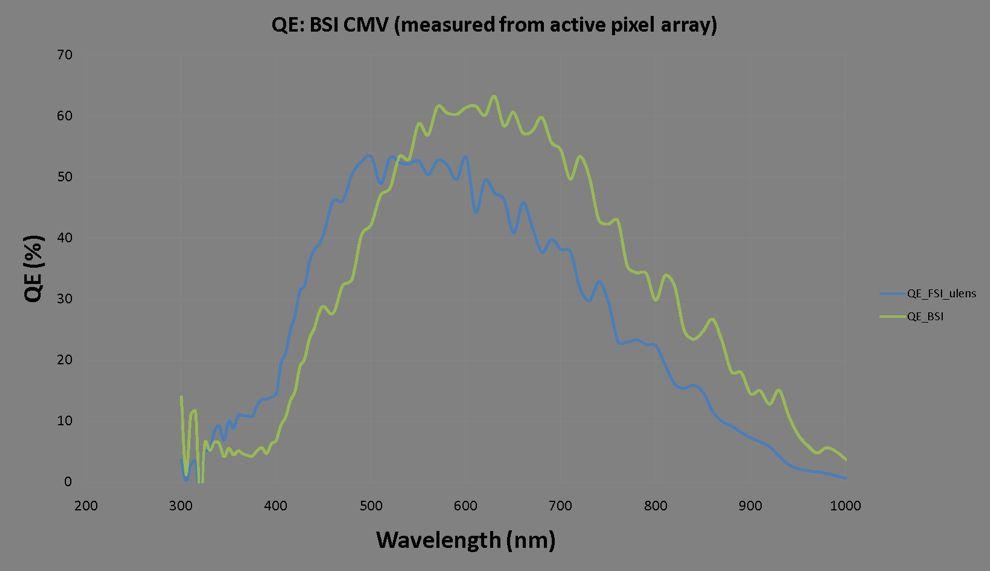
36 CMOSIS Technology differentiators Fast column AD converters Low noise global shutter pixels High frame rates Thin back-end process High dynamic range pixels Backside illumination technology
37 CMOSIS Core Technologies Global shutter pixels with low read noise, high shutter efficiency, and low FPN High speed on chip 10/12/14 bit column ADC s Backside Thinning and Illumination CMOS Time Delay and Integration (TDI) Radiation hardened CIS Large area (wafer scale) imagers with high yields (stitching!) CIS system-on-a-chip Very high frame rate imagers
38 CMOSIS Long Term R&D Plan Move to more advanced CMOS technologies: µm or below Smaller pixels More complex pixels Better electro-optical performance On chip image processing electronics > smart imagers Improved image sensor performances: Lower read noise: 1e- Increase full well: higher SNR High performance ADC: resolution, speed 1 GBit/s LVDS type interfaces
39 CMOSIS Long Term R&D Plan Smaller Technologies
40 Global shutter pixel smaller pixels Need for smaller optical formats & complex pixels smaller technologies 8 transistors, 2 source followers, 2 capacitors


41 The importance of a thin back-end even for a large pixel 6 µm pixel
42 CMOSIS moves to smaller technologies First tape-out s in 110/90 nm/300mm Moving to 90/65 nm/300mm

43 Excellent quantum efficiency
44 Excellent angular response > 95% at 20 angel

45 CMOSIS smaller architectures 300mm

46 CMOSIS smaller architectures 300mm
47 CMOSIS Long Term R&D Plan Back Side Illumination


48 Backside Illumination Address Many Challenges Dynamic Range Higher sensitivity Sensitivity Higher QE Frame Rate More readout lines Resolution Smaller pixels Angular Response No metal blocking Functionality More complex pixels Picture by Dr. Avi Strum, TowerJazz


49 High End Image Sensor Challenges Sensitivity Dynamic Range Frame Rate Resolution Functionality Angular Response Picture by Dr. Avi Strum, TowerJazz
50 Backside illumination: applications Scientific and industrial vision markets Performance : low noise, high QE Large pixels: MTF / cross-talk less problematic Monochrome Increased UV sensitivity: for inspection, analysis applications, EUV for science/space. Global shutter, without degradation of noise and PLS in BSI Performance: low dark current, good read noise Our developments focuses on this area

51 FSI & BSI CMV Mpixel 180 fps

52 FSI & BSI CMV Mpixel 340 fps
, Excellent PLS: 1/20,000 best in world for BSI global shutter")

53 CMOSIS Back Side Illumination Development on CMOSIS CMV2000 / CMV4000te (EUV), Excellent PLS: 1/20,000 best in world for BSI global shutter sensor Not (only) for visible light QE improvement Extension of sensitivity to UV, EUV, electron detection Frontside CMV2000 with µlens Backside CMV2000


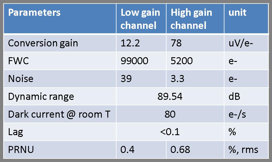
54 Backside illumination: quantum efficiency + improvement of yield (hot clusters)
55 Cause of low sensitivity in blue & UV Dead-zone below 450nm caused by pre-doped profile outdiffusing during CMOS processing.
56 Solutions to enhance blue response Get rid of the dead zone through either: 1. Backside implant + (laser) anneal with Excico Laser 2. Further etching of the silicon 3. Deposition of a layer with fixed negative charge (Sapphire Al 2 O 3 ) 4. A combination of 2 & 3
57 QE further etch improves QE again Some improvement in blue but not good enough yet 57
58 CMOSIS BSI Flow Start material: SOI wafer specific doping profile! Backside implant! Silicon etch! Wafer processing:! 0.18 µm CMOS! Laser anneal! Al2O deposition! Wafer test! AR coating (+CFA, )! Wafer bonding! (adhesive or ox-ox)! Thinning - stop on BOX! Pad opening! Packaging (assembly)! BOX etch! Final test! CMOSIS Proprietary Flow
59 CMOSIS Long Term R&D Plan > High Dynamic Range

60 More dynamic range with 2 transfer gates FD2 TX2 PPD_P TX1 FD1 Out image1 PPD_N P- epi Pixel with 2 floating diffusions First transfer to smallest FD High gain for dark signals Second transfer of remaining photocharges to larger FD low gain for bright signals 2 outputs per pixel Simplification: select which FD to use based upon required gain. C fd1 << C fd2 FD2 FD1 image2 illumination TX1 PPD TX2

61 CLN db + 70 db = 90 db
62 CLN1000 CHARACTERIZATION TABLE

63 CLN1000 SENSOR FUNCTIONALITY LOW GAIN CHANNEL HIGH GAIN CHANNEL
 remove! Excellent QE in UV Future development! Digital out (on-chip column-level ADC)! Timing on-chip!")
64 High Dynamic Range & BSI BSI version:! Fully functional! SOI start material: 3um epi! Customized post-processing! Buried oxide (BOX) remove! Excellent QE in UV Future development! Digital out (on-chip column-level ADC)! Timing on-chip! Full product
65 QE 10 µm pixel, 3 µm thickness BSI UV sensitivity


66 CMOSIS Manufacturing Flow Fabs: - 110/90nm - 90/65nm - 180nm - 180nm - 180nm - 180nm
67 Thanks' for your attention! More Imaging Luc De Mey - CEO - CMOSIS SA Annual Review / June 28, 2011
Jan Bogaerts imec
 imec 2007 1 Radiometric Performance Enhancement of APS 3 rd Microelectronic Presentation Days, Estec, March 7-8, 2007 Outline Introduction Backside illuminated APS detector Approach CMOS APS (readout)
CMOS Today & Tomorrow
 CMOS Today & Tomorrow Uwe Pulsfort TDALSA Product & Application Support Overview Image Sensor Technology Today Typical Architectures Pixel, ADCs & Data Path Image Quality Image Sensor Technology Tomorrow
High-end CMOS Active Pixel Sensor for Hyperspectral Imaging
 R11 High-end CMOS Active Pixel Sensor for Hyperspectral Imaging J. Bogaerts (1), B. Dierickx (1), P. De Moor (2), D. Sabuncuoglu Tezcan (2), K. De Munck (2), C. Van Hoof (2) (1) Cypress FillFactory, Schaliënhoevedreef
e2v Launches New Onyx 1.3M for Premium Performance in Low Light Conditions
 e2v Launches New Onyx 1.3M for Premium Performance in Low Light Conditions e2v s Onyx family of image sensors is designed for the most demanding outdoor camera and industrial machine vision applications,
Simulation of High Resistivity (CMOS) Pixels
 Pixels") Simulation of High Resistivity (CMOS) Pixels Stefan Lauxtermann, Kadri Vural Sensor Creations Inc. AIDA-2020 CMOS Simulation Workshop May 13 th 2016 OUTLINE 1. Definition of High Resistivity Pixel Also
Simulation of High Resistivity (CMOS) Pixels Stefan Lauxtermann, Kadri Vural Sensor Creations Inc. AIDA-2020 CMOS Simulation Workshop May 13 th 2016 OUTLINE 1. Definition of High Resistivity Pixel Also
Design and Performance of a Pinned Photodiode CMOS Image Sensor Using Reverse Substrate Bias
 Design and Performance of a Pinned Photodiode CMOS Image Sensor Using Reverse Substrate Bias 13 September 2017 Konstantin Stefanov Contents Background Goals and objectives Overview of the work carried
Fundamentals of CMOS Image Sensors
 CHAPTER 2 Fundamentals of CMOS Image Sensors Mixed-Signal IC Design for Image Sensor 2-1 Outline Photoelectric Effect Photodetectors CMOS Image Sensor(CIS) Array Architecture CIS Peripherals Design Considerations
A 120dB dynamic range image sensor with single readout using in pixel HDR
 A 120dB dynamic range image sensor with single readout using in pixel HDR CMOS Image Sensors for High Performance Applications Workshop November 19, 2015 J. Caranana, P. Monsinjon, J. Michelot, C. Bouvier,
A 1Mjot 1040fps 0.22e-rms Stacked BSI Quanta Image Sensor with Cluster-Parallel Readout
 A 1Mjot 1040fps 0.22e-rms Stacked BSI Quanta Image Sensor with Cluster-Parallel Readout IISW 2017 Hiroshima, Japan Saleh Masoodian, Jiaju Ma, Dakota Starkey, Yuichiro Yamashita, Eric R. Fossum May 2017
Image sensor combining the best of different worlds
 Image sensors and vision systems Image sensor combining the best of different worlds First multispectral time-delay-and-integration (TDI) image sensor based on CCD-in-CMOS technology. Introduction Jonathan
European Low Flux CMOS Image Sensor
 European Low Flux CMOS Image Sensor Description and Preliminary Results Ajit Kumar Kalgi 1, Wei Wang 1, Bart Dierickx 1, Dirk Van Aken 1, Kaiyuan Wu 1, Alexander Klekachev 1, Gerlinde Ruttens 1, Kyriaki
TAOS II: Three 88-Megapixel astronomy arrays of large area, backthinned, and low-noise CMOS sensors
 TAOS II: Three 88-Megapixel astronomy arrays of large area, backthinned, and low-noise CMOS sensors CMOS Image Sensors for High Performance Applications TOULOUSE WORKSHOP - 26th & 27th NOVEMBER 2013 Jérôme
LINCE5M 5.2 MEGAPIXELS, 1 INCH, 250FPS, GLOBAL SHUTTER CMOS IMAGE SENSOR. anafocus.com
 LINCE5M 5.2 MEGAPIXELS, 1 INCH, 250FPS, GLOBAL SHUTTER CMOS IMAGE SENSOR anafocus.com WE PARTNER WITH OUR CUSTOMERS TO IMPROVE, SAVE AND PROTECT PEOPLE S LIVES OVERVIEW Lince5M is a digital high speed
Vision 2016 Highlights
 10 Vision 2016 Highlights Contributions to the Press map. Jan Vermeiren, Business Development Manager Your Presentation Title 2 Caeleste Mission Statement THE Supplier of Beyond state-of-the-art Custom
IRIS3 Visual Monitoring Camera on a chip
 IRIS3 Visual Monitoring Camera on a chip ESTEC contract 13716/99/NL/FM(SC) G.Meynants, J.Bogaerts, W.Ogiers FillFactory, Mechelen (B) T.Cronje, T.Torfs, C.Van Hoof IMEC, Leuven (B) Microelectronics Presentation
BACKSIDE ILLUMINATED CMOS-TDI LINE SCANNER FOR SPACE APPLICATIONS
 BACKSIDE ILLUMINATED CMOS-TDI LINE SCANNER FOR SPACE APPLICATIONS O. Cohen, N. Ben-Ari, I. Nevo, N. Shiloah, G. Zohar, E. Kahanov, M. Brumer, G. Gershon, O. Ofer SemiConductor Devices (SCD) P.O.B. 2250,
EVALUATION OF RADIATION HARDNESS DESIGN TECHNIQUES TO IMPROVE RADIATION TOLERANCE FOR CMOS IMAGE SENSORS DEDICATED TO SPACE APPLICATIONS
 EVALUATION OF RADIATION HARDNESS DESIGN TECHNIQUES TO IMPROVE RADIATION TOLERANCE FOR CMOS IMAGE SENSORS DEDICATED TO SPACE APPLICATIONS P. MARTIN-GONTHIER, F. CORBIERE, N. HUGER, M. ESTRIBEAU, C. ENGEL,
High QE, Thinned Backside-Illuminated, 3e- RoN, Fast 700fps, 1760x1760 Pixels Wave-Front Sensor Imager with Highly Parallel Readout
 High QE, Thinned Backside-Illuminated, 3e- RoN, Fast 700fps, 1760x1760 Pixels Wave-Front Sensor Imager with Highly Parallel Readout Mark Downing, Dietrich Baade, Norbert Hubin, Olaf Iwert, Javier Reyes
ABSTRACT. Section I Overview of the µdss
 An Autonomous Low Power High Resolution micro-digital Sun Sensor Ning Xie 1, Albert J.P. Theuwissen 1, 2 1. Delft University of Technology, Delft, the Netherlands; 2. Harvest Imaging, Bree, Belgium; ABSTRACT
CMOS Image Sensors in Cell Phones, Cars and Beyond. Patrick Feng General manager BYD Microelectronics October 8, 2013
 CMOS Image Sensors in Cell Phones, Cars and Beyond Patrick Feng General manager BYD Microelectronics October 8, 2013 BYD Microelectronics (BME) is a subsidiary of BYD Company Limited, Shenzhen, China.
Chapter 4 Vertex. Qun Ouyang. Nov.10 th, 2017Beijing. CEPC detector CDR mini-review
 Chapter 4 Vertex Qun Ouyang Nov.10 th, 2017Beijing Nov.10 h, 2017 CEPC detector CDR mini-review CEPC detector CDR mini-review Contents: 4 Vertex Detector 4.1 Performance Requirements and Detector Challenges
A 3 Mpixel ROIC with 10 m Pixel Pitch and 120 Hz Frame Rate Digital Output
 A 3 Mpixel ROIC with 10 m Pixel Pitch and 120 Hz Frame Rate Digital Output Elad Ilan, Niv Shiloah, Shimon Elkind, Roman Dobromislin, Willie Freiman, Alex Zviagintsev, Itzik Nevo, Oren Cohen, Fanny Khinich,
Image Sensor Solutions CMOSIS
 Image Sensor Solutions CMOSIS We provide advanced sensor solutions for the most challenging applications. Our portfolio ams is a global leader in the design and manufacture of advanced sensor solutions.
CCD1600A Full Frame CCD Image Sensor x Element Image Area
 - 1 - General Description CCD1600A Full Frame CCD Image Sensor 10560 x 10560 Element Image Area General Description The CCD1600 is a 10560 x 10560 image element solid state Charge Coupled Device (CCD)
Characterisation of a Novel Reverse-Biased PPD CMOS Image Sensor
 Characterisation of a Novel Reverse-Biased PPD CMOS Image Sensor Konstantin D. Stefanov, Andrew S. Clarke, James Ivory and Andrew D. Holland Centre for Electronic Imaging, The Open University, Walton Hall,
Monolithic Pixel Sensors in SOI technology R&D activities at LBNL
 Monolithic Pixel Sensors in SOI technology R&D activities at LBNL Lawrence Berkeley National Laboratory M. Battaglia, L. Glesener (UC Berkeley & LBNL), D. Bisello, P. Giubilato (LBNL & INFN Padova), P.
sensicam em electron multiplication digital 12bit CCD camera system
 sensicam em electron multiplication digital 12bit CCD camera system electron multiplication gain of up to 1000 superior resolution (1004 1002 pixel) for EMCCD extremely low noise < 1e excellent quantum
Measurement results of DIPIX pixel sensor developed in SOI technology
 Measurement results of DIPIX pixel sensor developed in SOI technology Mohammed Imran Ahmed a,b, Yasuo Arai c, Marek Idzik a, Piotr Kapusta b, Toshinobu Miyoshi c, Micha l Turala b a AGH University of Science
Electron-Bombarded CMOS
 New Megapixel Single Photon Position Sensitive HPD: Electron-Bombarded CMOS University of Lyon / CNRS-IN2P3 in collaboration with J. Baudot, E. Chabanat, P. Depasse, W. Dulinski, N. Estre, M. Winter N56:
Data Sheet SMX-160 Series USB2.0 Cameras
 Data Sheet SMX-160 Series USB2.0 Cameras SMX-160 Series USB2.0 Cameras Data Sheet Revision 3.0 Copyright 2001-2010 Sumix Corporation 4005 Avenida de la Plata, Suite 201 Oceanside, CA, 92056 Tel.: (877)233-3385;
Applications for cameras with CMOS-, CCD- and InGaAssensors. Jürgen Bretschneider AVT, 2014
 Applications for cameras with CMOS-, CCD- and InGaAssensors Jürgen Bretschneider AVT, 2014 Allied Vision Technologies Profile Foundation: 1989,Headquarters: Stadtroda (Thüringen), Employees: aprox. 265
Automotive Image Sensors
 Automotive Image Sensors February 1st 2018 Boyd Fowler and Johannes Solhusvik 1 Outline Automotive Image Sensor Market and Applications Viewing Sensors HDR Flicker Mitigation Machine Vision Sensors In
pco.1600 cooled digital 14bit CCD camera system
 pco.1600 cooled digital 14bit CCD camera system n excellent resolution (1600 1200 pixel) n 14 bit dynamic range n frame rate of 30 fps at full resolution n image memory in camera (camram up to 4 GB) n
Based on lectures by Bernhard Brandl
 Astronomische Waarneemtechnieken (Astronomical Observing Techniques) Based on lectures by Bernhard Brandl Lecture 10: Detectors 2 1. CCD Operation 2. CCD Data Reduction 3. CMOS devices 4. IR Arrays 5.
STA1600LN x Element Image Area CCD Image Sensor
 ST600LN 10560 x 10560 Element Image Area CCD Image Sensor FEATURES 10560 x 10560 Photosite Full Frame CCD Array 9 m x 9 m Pixel 95.04mm x 95.04mm Image Area 100% Fill Factor Readout Noise 2e- at 50kHz
Minimizes reflection losses from UV to IR; No optical losses due to multiple optical surfaces; Optional AR coating and wedge windows available.
 SOPHIA: 2048B The SOPHIA : 2048B camera from Princeton Instruments (PI) is fully integrated, ultra-low noise 2048 x 2048, 15 µm pixel CCD camera designed expressly for the most demanding quantitative scientific
pco.edge 4.2 LT 0.8 electrons 2048 x 2048 pixel 40 fps up to :1 up to 82 % pco. low noise high resolution high speed high dynamic range
 edge 4.2 LT scientific CMOS camera high resolution 2048 x 2048 pixel low noise 0.8 electrons USB 3.0 small form factor high dynamic range up to 37 500:1 high speed 40 fps high quantum efficiency up to
High Definition 10µm pitch InGaAs detector with Asynchronous Laser Pulse Detection mode
 High Definition 10µm pitch InGaAs detector with Asynchronous Laser Pulse Detection mode R. Fraenkel, E. Berkowicz, L. Bykov, R. Dobromislin, R. Elishkov, A. Giladi, I. Grimberg, I. Hirsh, E. Ilan, C. Jacobson,
Progress on Silicon-on-Insulator Monolithic Pixel Process
 Progress on Silicon-on-Insulator Monolithic Pixel Process Sep. 17, 2013 Vertex2013@Lake Starnberg Yasuo Arai, KEK yasuo.arai@kek.jp http://rd.kek.jp/project/soi/ 1 Outline Introduction Basic SOI Pixel
2 nd Generation CMOS Charge Transfer TDI: Results on Proton Irradiation
 2 nd Generation CMOS Charge Transfer TDI: Results on Proton Irradiation F. Mayer, J. Endicott, F. Devriere e2v, Avenue de Rochepleine, BP123, 38521 Saint Egrève Cedex, France J. Rushton, K. Stefanov, A.
STM RH-ASIC capability
 STM RH-ASIC capability JAXA 24 th MicroElectronic Workshop 13 th 14 th October 2011 Prepared by STM Crolles and AeroSpace Unit Deep Sub Micron (DSM) is strategic for Europe Strategic importance of European
Integrating Additional Functionality with APS Sensors
 Integrating Additional Functionality with APS Sensors Microelectronics Presentation Days ESA/ESTEC 8 th March 2007 Werner Ogiers (fwo [at] cypress.com) Cypress Semiconductor (Formerly Fillfactory B.V)
Automotive In-cabin Sensing Solutions. Nicolas Roux September 19th, 2018
 Automotive In-cabin Sensing Solutions Nicolas Roux September 19th, 2018 Impact of Drowsiness 2 Drowsiness responsible for 20% to 25% of car crashes in Europe (INVS/AFSA) Beyond Drowsiness Driver Distraction
A 3MPixel Multi-Aperture Image Sensor with 0.7µm Pixels in 0.11µm CMOS
 A 3MPixel Multi-Aperture Image Sensor with 0.7µm Pixels in 0.11µm CMOS Keith Fife, Abbas El Gamal, H.-S. Philip Wong Stanford University, Stanford, CA Outline Introduction Chip Architecture Detailed Operation
TDI-CMOS Image Sensor for Earth Observation
 TDI-CMOS Image Sensor for Earth Observation Jérôme Pratlong *a, Paul Jerram a, Georgios Tsiolis a, Vincent Arkesteijn b ; Paul Donegan c ; Laurens Korthout d a Teledyne-e2v, Waterhouse Lane, Chelmsford,
Selecting an image sensor for the EJSM VIS/NIR camera systems
 Selecting an image sensor for the EJSM VIS/NIR camera systems presented by Harald Michaelis (DLR-PF) Folie 1 EJSM- Jan. 18th 2010; ESTEC What for a detector/sensor we shall chose for EJSM? Vortragstitel
A scientific HDR Multi-spectral imaging platform. B. Dupont, Pyxalis, France.
 A scientific HDR Multi-spectral imaging platform B. Dupont, Pyxalis, France. OUTLINE HDPYX HDR Scientific Sensor platform First usage as hyperspectral device by Resolution Spectra and CSUG Perspectives
Low temperature measurements of the large-area, backthinned, and lownoise TAOSII CMOS sensors
 Low temperature measurements of the large-area, backthinned, and lownoise TAOSII CMOS sensors Steven Johnson, Jérôme Pratlong, Amr Ibrahim, Paul Jerram, Paul Jorden (e2v technologies) Shiang-Yu Wang and
ACTIVE PIXEL SENSORS VS. CHARGE-COUPLED DEVICES
 ACTIVE PIXEL SENSORS VS. CHARGE-COUPLED DEVICES Dr. Eric R. Fossum Imaging Systems Section Jet Propulsion Laboratory, California Institute of Technology (818) 354-3128 1993 IEEE Workshop on CCDs and Advanced
Advanced Camera and Image Sensor Technology. Steve Kinney Imaging Professional Camera Link Chairman
 Advanced Camera and Image Sensor Technology Steve Kinney Imaging Professional Camera Link Chairman Content Physical model of a camera Definition of various parameters for EMVA1288 EMVA1288 and image quality
panda family ultra compact scmos cameras
 panda family ultra compact scmos cameras up to 95 % quantum efficiency 6.5 µm pixel size for a perfect fit in microscopy and life science applications 65 mm ultra compact design specifications panda family
Development of CMOS pixel sensors for tracking and vertexing in high energy physics experiments
 PICSEL group Development of CMOS pixel sensors for tracking and vertexing in high energy physics experiments Serhiy Senyukov (IPHC-CNRS Strasbourg) on behalf of the PICSEL group 7th October 2013 IPRD13,
CCDS. Lesson I. Wednesday, August 29, 12
 CCDS Lesson I CCD OPERATION The predecessor of the CCD was a device called the BUCKET BRIGADE DEVICE developed at the Phillips Research Labs The BBD was an analog delay line, made up of capacitors such
Lecture: Integration of silicon photonics with electronics. Prepared by Jean-Marc FEDELI CEA-LETI
 Lecture: Integration of silicon photonics with electronics Prepared by Jean-Marc FEDELI CEA-LETI Context The goal is to give optical functionalities to electronics integrated circuit (EIC) The objectives
CMOS Imagers : Today and Tomorrow
 CMOS Imagers : Today and Tomorrow IISW2015 Highlights Albert Theuwissen Harvest Imaging (B) Image Capturing Circle the Netherlands Belgium Harvest Imaging Germany France copyright 2010 Albert Theuwissen
Last class. This class. CCDs Fancy CCDs. Camera specs scmos
 CCDs and scmos Last class CCDs Fancy CCDs This class Camera specs scmos Fancy CCD cameras: -Back thinned -> higher QE -Unexposed chip -> frame transfer -Electron multiplying -> higher SNR -Fancy ADC ->
IISW 2009 Backside Illumination Symposium
 IISW 2009 Backside Illumination Symposium The Mass Production of BSI CMOS Imager Sensors Dr. Howard Rhodes Omnivision Technologies, Inc. 1 Acknowlegement D. Tai, Y. Qian, D. Mao, V. Venezia, Wei Zheng,
FUTURE PROSPECTS FOR CMOS ACTIVE PIXEL SENSORS
 FUTURE PROSPECTS FOR CMOS ACTIVE PIXEL SENSORS Dr. Eric R. Fossum Jet Propulsion Laboratory Dr. Philip H-S. Wong IBM Research 1995 IEEE Workshop on CCDs and Advanced Image Sensors April 21, 1995 CMOS APS
Backside illuminated CMOS-TDI line scan sensor for space applications
 Backside illuminated CMOS-TDI line scan sensor for space applications Omer COHEN, Oren OFER, Gil ABRAMOVICH, Nimrod BEN-ARI, Gal GERSHON, Maya BRUMER, Adi SHAY, Yaron SHAMAY SemiConductor Devices (SCD)
CMOS 0.18 m SPAD. TowerJazz February, 2018 Dr. Amos Fenigstein
 CMOS 0.18 m SPAD TowerJazz February, 2018 Dr. Amos Fenigstein Outline CMOS SPAD motivation Two ended vs. Single Ended SPAD (bulk isolated) P+/N two ended SPAD and its optimization Application of P+/N two
Photolithography I ( Part 1 )
") 1 Photolithography I ( Part 1 ) Chapter 13 : Semiconductor Manufacturing Technology by M. Quirk & J. Serda Bjørn-Ove Fimland, Department of Electronics and Telecommunication, Norwegian University of Science
1 Photolithography I ( Part 1 ) Chapter 13 : Semiconductor Manufacturing Technology by M. Quirk & J. Serda Bjørn-Ove Fimland, Department of Electronics and Telecommunication, Norwegian University of Science
Factors Affecting Pixel Scaling Limits for cellphone imaging systems
 Factors Affecting Pixel Scaling Limits for cellphone imaging systems October 28, 2010 Richard Crisp rcrisp@narrowbandimaging.com Agenda Pixel Scaling Limits Optical Considerations Image Sensor Considerations
Micron MT9T Megapixel, ¼ Optical Format, 1.75 µm Pixel Size System-on-Chip (SOC) CMOS Image Sensor
 CMOS Image Sensor") Micron MT9T111 3.1 Megapixel, ¼ Optical Format, 1.75 µm Pixel Size System-on-Chip (SOC) CMOS Image Sensor Imager Process Review with Optional TEM Analysis of SRAM For comments, questions, or more information
Micron MT9T111 3.1 Megapixel, ¼ Optical Format, 1.75 µm Pixel Size System-on-Chip (SOC) CMOS Image Sensor Imager Process Review with Optional TEM Analysis of SRAM For comments, questions, or more information
imec image sensors and vision systems
 imec image sensors and vision systems maarten.willems@imec.be IMEC FOCUS: SPECIALTY IMAGING Design innovation Process Technologies Machine Vision Industrial Instrumentation Key features: High speed Low
CMOSIS CMV Mp, 5.5 µm Pixel Pitch High-Speed Pipelined Global Shutter CMOS Image Sensor with Correlated Double Sampling
 CMOSIS CMV4000 4 Mp, 5.5 µm Pixel Pitch High-Speed Pipelined Global Shutter CMOS Image Sensor with Correlated Double Sampling Imager Process Review 3685 Richmond Road, Suite 500, Ottawa, ON K2H 5B7 Canada
A SPAD-Based, Direct Time-of-Flight, 64 Zone, 15fps, Parallel Ranging Device Based on 40nm CMOS SPAD Technology
 A SPAD-Based, Direct Time-of-Flight, 64 Zone, 15fps, Parallel Ranging Device Based on 40nm CMOS SPAD Technology Pascal Mellot / Bruce Rae 27 th February 2018 Summary 2 Introduction to ranging device Summary
200mm and 300mm Test Patterned Wafers for Bonding Process Applications SKW ASSOCIATES, INC.
 C M P C h a r a c t e r I z a t I o n S o l u t I o n s 200mm and 300mm Test Patterned Wafers for Bonding Process Applications SKW ASSOCIATES, INC. 2920 Scott Blvd., Santa Clara, CA 95054 Tel: 408-919-0094,
IT FR R TDI CCD Image Sensor
 4k x 4k CCD sensor 4150 User manual v1.0 dtd. August 31, 2015 IT FR 08192 00 R TDI CCD Image Sensor Description: With the IT FR 08192 00 R sensor ANDANTA GmbH builds on and expands its line of proprietary
Characterisation of a CMOS Charge Transfer Device for TDI Imaging
 Preprint typeset in JINST style - HYPER VERSION Characterisation of a CMOS Charge Transfer Device for TDI Imaging J. Rushton a, A. Holland a, K. Stefanov a and F. Mayer b a Centre for Electronic Imaging,
Sony IMX Megapixel, 1.4 µm Pixel 1/3.2 Optical Format CMOS Image Sensor
 Sony IMX046 8.11 Megapixel, 1.4 µm Pixel 1/3.2 Optical Format CMOS Image Sensor Imager Process Review For comments, questions, or more information about this report, or for any additional technical needs
EE 392B: Course Introduction
 EE 392B Course Introduction About EE392B Goals Topics Schedule Prerequisites Course Overview Digital Imaging System Image Sensor Architectures Nonidealities and Performance Measures Color Imaging Recent
CCDs for Earth Observation James Endicott 1 st September th UK China Workshop on Space Science and Technology, Milton Keynes, UK
 CCDs for Earth Observation James Endicott 1 st September 2011 7 th UK China Workshop on Space Science and Technology, Milton Keynes, UK Introduction What is this talk all about? e2v sensors in spectrometers
Detectors for microscopy - CCDs, APDs and PMTs. Antonia Göhler. Nov 2014
 Detectors for microscopy - CCDs, APDs and PMTs Antonia Göhler Nov 2014 Detectors/Sensors in general are devices that detect events or changes in quantities (intensities) and provide a corresponding output,
: fps. pco.edge. 1.4 electrons. 5.5 megapixel. pco. high speed. high resolution. low noise. high dynamic range. scientific CMOS camera
 edge scientific CMOS camera low noise 1.4 electrons high resolution 5.5 megapixel high speed high dynamic range 22 000 :1 100 fps The new edge is a breakthrough in scientific imaging cameras, due to its
ABSTRACT. Keywords: 0,18 micron, CMOS, APS, Sunsensor, Microned, TNO, TU-Delft, Radiation tolerant, Low noise. 1. IMAGERS FOR SPACE APPLICATIONS.
 Active pixel sensors: the sensor of choice for future space applications Johan Leijtens(), Albert Theuwissen(), Padmakumar R. Rao(), Xinyang Wang(), Ning Xie() () TNO Science and Industry, Postbus, AD
Welcome to: LMBR Imaging Workshop. Imaging Fundamentals Mike Meade, Photometrics
 Welcome to: LMBR Imaging Workshop Imaging Fundamentals Mike Meade, Photometrics Introduction CCD Fundamentals Typical Cooled CCD Camera Configuration Shutter Optic Sealed Window DC Voltage Serial Clock
Fully depleted, thick, monolithic CMOS pixels with high quantum efficiency
 Fully depleted, thick, monolithic CMOS pixels with high quantum efficiency Andrew Clarke a*, Konstantin Stefanov a, Nicholas Johnston a and Andrew Holland a a Centre for Electronic Imaging, The Open University,
KAI 2015 Innovation Award for CMOSIS Germany GmbH - CMOSIS - CMOS Image Sensors
 KAI 2015 Innovation Award for CMOSIS Germany GmbH - CMOSIS - CMOS Image Sensors Page 1 TABLE OF CONTENTS About Cmosis... 3 Orion Line Scan... 4 CMV50000... 6 Orion USB3 Eval Kit... 8 CMV2000... 10 NanEye...
Minimizes reflection losses from UV-IR; Optional AR coatings & wedge windows are available.
 Now Powered by LightField PyLoN:2K 2048 x 512 The PyLoN :2K is a controllerless, cryogenically-cooled CCD camera designed for quantitative scientific spectroscopy applications demanding the highest possible
CMOS sensor for TAOS 2
 CMOS sensor for TAOS 2 Shiang-Yu Wang ( 王祥宇 ) Academia Sinica, Institute of Astronomy & Astrophysics Taiwan American Occultation Survey Institute of Astronomy & Astrophysics, Academia Sinica, Taiwan Sun-Kun
MagnaChip MC511DB 1.3 Megapixel CMOS Image Sensor 0.18 µm Process
 MagnaChip MC511DB 1.3 Megapixel CMOS Image Sensor 0.18 µm Process Imager Process Review For comments, questions, or more information about this report, or for any additional technical needs concerning

CMOS MT9V034 Camera Module 1/3-Inch 0.36MP Monochrome Module Datasheet
 CMOS MT9V034 Camera Module 1/3-Inch 0.36MP Monochrome Module Datasheet Rev 1.0, Mar 2017 Table of Contents 1 Introduction... 2 2 Features... 3 3 Block Diagram... 3 4 Application... 3 5 Pin Definition...
Tests of monolithic CMOS SOI pixel detector prototype INTPIX3 MOHAMMED IMRAN AHMED. Supervisors Dr. Henryk Palka (IFJ-PAN) Dr. Marek Idzik(AGH-UST)
 Dr. Marek Idzik(AGH-UST)") Internal Note IFJ PAN Krakow (SOIPIX) Tests of monolithic CMOS SOI pixel detector prototype INTPIX3 by MOHAMMED IMRAN AHMED Supervisors Dr. Henryk Palka (IFJ-PAN) Dr. Marek Idzik(AGH-UST) Test and Measurement
Internal Note IFJ PAN Krakow (SOIPIX) Tests of monolithic CMOS SOI pixel detector prototype INTPIX3 by MOHAMMED IMRAN AHMED Supervisors Dr. Henryk Palka (IFJ-PAN) Dr. Marek Idzik(AGH-UST) Test and Measurement
Production of HPDs for the LHCb RICH Detectors
 Production of HPDs for the LHCb RICH Detectors LHCb RICH Detectors Hybrid Photon Detector Production Photo Detector Test Facilities Test Results Conclusions IEEE Nuclear Science Symposium Wyndham, 24 th
Aptina MT9P111 5 Megapixel, 1/4 Inch Optical Format, System-on-Chip (SoC) CMOS Image Sensor
 CMOS Image Sensor") Aptina MT9P111 5 Megapixel, 1/4 Inch Optical Format, System-on-Chip (SoC) CMOS Image Sensor Imager Process Review For comments, questions, or more information about this report, or for any additional technical
Aptina MT9P111 5 Megapixel, 1/4 Inch Optical Format, System-on-Chip (SoC) CMOS Image Sensor Imager Process Review For comments, questions, or more information about this report, or for any additional technical
ULS24 Frequently Asked Questions
 List of Questions 1 1. What type of lens and filters are recommended for ULS24, where can we source these components?... 3 2. Are filters needed for fluorescence and chemiluminescence imaging, what types
CCD and CMOS Imaging Devices for Large (Ground Based) Telescopes. Veljko Radeka BNL SNIC April 3, 2006
 Telescopes. Veljko Radeka BNL SNIC April 3, 2006") CCD and CMOS Imaging Devices for Large (Ground Based) Telescopes Veljko Radeka BNL SNIC April 3, 2006 1 Large Telescopes Survey telescope Deep probe Primary Mirror dia.=d m, Area= A Large (~8m) Very large
CCD and CMOS Imaging Devices for Large (Ground Based) Telescopes Veljko Radeka BNL SNIC April 3, 2006 1 Large Telescopes Survey telescope Deep probe Primary Mirror dia.=d m, Area= A Large (~8m) Very large
Neuromorphic Event-Based Vision Sensors
 Inst. of Neuroinformatics www.ini.uzh.ch Conventional cameras (aka Static vision sensors) deliver a stroboscopic sequence of frames Silicon Retina Technology Tobi Delbruck Inst. of Neuroinformatics, University
Introduction to Computer Vision
 Introduction to Computer Vision CS / ECE 181B Thursday, April 1, 2004 Course Details HW #0 and HW #1 are available. Course web site http://www.ece.ucsb.edu/~manj/cs181b Syllabus, schedule, lecture notes,
Back-illuminated scientific CMOS camera. Datasheet
 Back-illuminated scientific CMOS camera Datasheet Breakthrough Technology KURO DATASHEET Highlights The KURO from Princeton Instruments is the world s first scientific CMOS (scmos) camera system to implement
400BSI V2.0. BSI Scientific CMOS Cooled Camera. 4 0 fps. 7 4 fps. 1.2 e % PRNU. 0.2 e μm 4.2 MP.
 4BSI V2. BSI Scientific CMOS Cooled Camera 1 QExFF (%) 8 6 4 2 2 4 6 8 1 11 Wavelength(nm) 7 4 fps CameraLink Faster Capture 4 fps USB3..2 e - DSNU.3 % PRNU More Accurate 1.2 e - Read Noise 6.5 μm Pixel
CMOS Digital Integrated Circuits Lec 2 Fabrication of MOSFETs
 CMOS Digital Integrated Circuits Lec 2 Fabrication of MOSFETs 1 CMOS Digital Integrated Circuits 3 rd Edition Categories of Materials Materials can be categorized into three main groups regarding their
Time Delay Integration (TDI), The Answer to Demands for Increasing Frame Rate/Sensitivity? Craige Palmer Assistant Sales Manager
, The Answer to Demands for Increasing Frame Rate/Sensitivity? Craige Palmer Assistant Sales Manager") Time Delay Integration (TDI), The Answer to Demands for Increasing Frame Rate/Sensitivity? Craige Palmer Assistant Sales Manager Laser Scanning Microscope High Speed Gated PMT Module High Speed Gating
Time Delay Integration (TDI), The Answer to Demands for Increasing Frame Rate/Sensitivity? Craige Palmer Assistant Sales Manager Laser Scanning Microscope High Speed Gated PMT Module High Speed Gating
First Results of 0.15µm CMOS SOI Pixel Detector
 First Results of 0.15µm CMOS SOI Pixel Detector Y. Arai, M. Hazumi, Y. Ikegami, T. Kohriki, O. Tajima, S. Terada, T. Tsuboyama, Y. Unno, H. Ushiroda IPNS, High Energy Accelerator Reserach Organization
Charged Coupled Device (CCD) S.Vidhya
 S.Vidhya") Charged Coupled Device (CCD) S.Vidhya 02.04.2016 Sensor Physical phenomenon Sensor Measurement Output A sensor is a device that measures a physical quantity and converts it into a signal which can be read
Charged Coupled Device (CCD) S.Vidhya 02.04.2016 Sensor Physical phenomenon Sensor Measurement Output A sensor is a device that measures a physical quantity and converts it into a signal which can be read
High Resolution 640 x um Pitch InSb Detector
 High Resolution 640 x 512 15um Pitch InSb Detector Chen-Sheng Huang, Bei-Rong Chang, Chien-Te Ku, Yau-Tang Gau, Ping-Kuo Weng* Materials & Electro-Optics Division National Chung Shang Institute of Science
TDI Imaging: An Efficient AOI and AXI Tool
 TDI Imaging: An Efficient AOI and AXI Tool Yakov Bulayev Hamamatsu Corporation Bridgewater, New Jersey Abstract As a result of heightened requirements for quality, integrity and reliability of electronic
Improved sensitivity high-definition interline CCD using the KODAK TRUESENSE Color Filter Pattern
 Improved sensitivity high-definition interline CCD using the KODAK TRUESENSE Color Filter Pattern James DiBella*, Marco Andreghetti, Amy Enge, William Chen, Timothy Stanka, Robert Kaser (Eastman Kodak
Reference: CMV2000-datasheet-v2.13. CMV2000 v2 Datasheet Page 1 of Megapixel machine vision CMOS image sensor. Datasheet.
 CMV2000 v2 Datasheet Page 1 of 63 2.2 Megapixel machine vision CMOS image sensor Datasheet CMV2000 v2 Datasheet Page 2 of 63 Change record Issue Date Modification 1 06/05/2009 Origination 1.1 12/11/2009